WO2025004337A1 - 光通信モジュール - Google Patents
光通信モジュール Download PDFInfo
- Publication number
- WO2025004337A1 WO2025004337A1 PCT/JP2023/024397 JP2023024397W WO2025004337A1 WO 2025004337 A1 WO2025004337 A1 WO 2025004337A1 JP 2023024397 W JP2023024397 W JP 2023024397W WO 2025004337 A1 WO2025004337 A1 WO 2025004337A1
- Authority
- WO
- WIPO (PCT)
- Prior art keywords
- optical
- circuit chip
- communication module
- transmitter
- receiver
- Prior art date
- Legal status (The legal status is an assumption and is not a legal conclusion. Google has not performed a legal analysis and makes no representation as to the accuracy of the status listed.)
- Ceased
Links
Images





Classifications
-
- G—PHYSICS
- G02—OPTICS
- G02B—OPTICAL ELEMENTS, SYSTEMS OR APPARATUS
- G02B6/00—Light guides; Structural details of arrangements comprising light guides and other optical elements, e.g. couplings
- G02B6/10—Light guides; Structural details of arrangements comprising light guides and other optical elements, e.g. couplings of the optical waveguide type
- G02B6/12—Light guides; Structural details of arrangements comprising light guides and other optical elements, e.g. couplings of the optical waveguide type of the integrated circuit kind
-
- G—PHYSICS
- G02—OPTICS
- G02B—OPTICAL ELEMENTS, SYSTEMS OR APPARATUS
- G02B6/00—Light guides; Structural details of arrangements comprising light guides and other optical elements, e.g. couplings
- G02B6/24—Coupling light guides
- G02B6/26—Optical coupling means
- G02B6/30—Optical coupling means for use between fibre and thin-film device
Definitions
- the present invention relates to an optical communication module, and more specifically, to an optical communication module that includes multiple transmission/reception units, each of which includes an optical transmitter and an optical receiver.
- optical communication modules and optical devices are not limited to long-distance communications; they are also used for links between data centers, between mobile phone base stations, and between edge routers, and there is an increasing demand for improved performance.
- electronic devices that process electrical signals ICs such as DSPs, drivers, and TIAs
- CPO copackaged optics
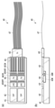
- Figure 1 shows the configuration of a conventional optical communications module with optical transmission and reception functions.
- Figure 1(a) shows the arrangement of each chip as viewed from the top of an optical communications module 10.
- Two sets of transmission and reception units each consisting of a digital signal processing circuit chip (DSP) 12, a driver circuit chip (DRV) 13, a transimpedance amplifier circuit chip (TIA) 14, an optical circuit chip 15, and a fiber array (FA) 16, are mounted on a package substrate 11. Input and output of optical signals are performed by optical fiber 17 via the FA 16.
- DSP digital signal processing circuit chip
- DDRV driver circuit chip
- TIA transimpedance amplifier circuit chip
- FA fiber array
- the DRV 13 amplifies the transmission electrical signal output from the DSP 12 and outputs it from the DRV output terminal group 13OUT.
- the TIA 14 receives the reception electrical signal output from the optical circuit chip 15 via the TIA input terminal group 14IN, amplifies it, and outputs it to the DSP 12.
- the optical circuit chip 15 includes an optical transmitter that includes an optical modulator, an optical waveguide, a splitter, an optical attenuator, etc., and an optical receiver that includes a photodiode (PD), an optical waveguide, an optical attenuator, etc. It also includes a group of transmission signal input terminals 15IN for inputting a transmission electrical signal from the DRV 13, and a group of reception signal output terminals 15OUT for outputting a reception electrical signal to the TIA 14.
- PD photodiode
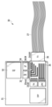
- FIG. 2 shows the configuration of an optical circuit chip of a conventional optical communication module.
- the optical circuit chip 15 is an optical device in which multiple circuit elements of an optical system and optical waveguides connecting them are integrated.
- Many optical transmitters TX use a Mach-Zehnder interferometer (MZI) type optical modulator MOD that utilizes the electro-optic effect.
- MZI type modulator MOD a traveling wave electrode 15E is arranged on an optical waveguide in the optical axis direction from the input end that inputs the CW light from the light source to the output end that outputs the transmitted optical signal.
- the traveling wave electrode 15E needs to have a certain length, and it specifies the length in the optical axis direction of the MZI type modulator MOD.
- the length in the optical axis direction of the MZI type modulator MOD is long, about 1 mm to 5 mm.
- the optical transmitter TX and the optical receiver RX are arranged in parallel, so the length of the optical circuit chip 15 in the optical axis direction depends on the length of the optical transmitter TX, i.e., the length of the modulator.
- the chip size of the optical circuit chip 15 becomes large, and there is space on the optical receiver RX side where no optical circuit elements are mounted, resulting in a problem of poor mounting efficiency of optical devices.
- the optical communication module 10 is configured with face-down mounting using a flip chip.
- the transmission signal input terminal group 15IN, the reception signal output terminal group 15OUT, and the traveling wave electrode 15E of the optical circuit chip 15 are formed on the bottom surface of the chip, and the configuration seen through from the top surface is shown diagrammatically in FIG. 1(a) and FIG. 2.
- FA16 indicates the form of end face connection connected to the end face of the optical circuit chip 15.
- Non-Patent Documents 1 and 2 it is also possible to apply a configuration in which an optical circuit chip mounted face-up is used to input and output optical signals from the top surface of the optical circuit using a grating coupler or the like.
- the DSP 12 has multiple transmit signal output terminals and receive signal input terminals on the side that outputs the transmit electrical signal to the optical transmitter TX and the side that inputs the receive electrical signal from the optical receiver (generally referred to as the line side).
- a digital signal processing circuit chip based on the 400GBASE-DR4 standard has a total of eight transmit signal output terminals with positive and negative phases for each of the four lanes, and a total of eight receive signal input terminals.
- the number of fibers connected to the fiber array is nine. Four each are used for transmitting and receiving optical signals, and one is used to input CW light from the light source to the optical transmitter TX.
- optical communications module 10 an example was shown in which two sets of transmitting and receiving units accommodating four lanes were implemented, but to increase the transmission capacity of the optical communications network, an optical communications module with double the sets of transmitting and receiving units can be manufactured.
- CPO it was necessary to connect the optical circuit chips 15 and fiber arrays 16 for each transmitting and receiving unit, which led to issues such as increased costs due to the increased number of parts and an increase in the size of the optical communications module.
- One embodiment of the present invention is an optical communications module having N (N is an even number) sets of transmission/reception units including optical transmitters and optical receivers, characterized in that for N digital signal processing circuit chips, K (K ⁇ N/2) optical circuit chips and K fiber arrays are provided, and along one side of the optical circuit chip, a group of transmission signal input terminals of the optical transmitter and a group of reception signal output terminals of the optical receiver are arranged, and the fiber array is connected to the side opposite to the one side.
- This configuration reduces the increase in costs associated with an increase in components and allows for the miniaturization of the optical communications module.
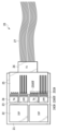
- FIG. 1 is a diagram showing the configuration of a conventional optical communication module having an optical transmission and reception function.
- FIG. 2 is a diagram showing the configuration of an optical circuit chip in a conventional optical communication module;
- FIG. 3 is a diagram showing a configuration of an optical communication module according to a first embodiment of the present invention;
- FIG. 4 is a diagram showing a configuration of an optical communication module according to a second embodiment of the present invention;
- FIG. 5 is a diagram showing the configuration of an optical circuit chip of an optical communication module according to a second embodiment;
- FIG. 6 is a diagram showing a configuration of an optical communication module according to a third embodiment of the present invention;
- FIG. 7 is a diagram showing a first example of an optical circuit chip of an optical communication module according to a third embodiment;
- FIG. 8 is a diagram showing a second example of the optical circuit chip of the optical communication module according to the third embodiment
- FIG. 9 is a diagram showing a third example of the optical circuit chip of the optical communication module according to the third embodiment
- FIG. 10 is a diagram showing a configuration of an optical communication module according to a fourth embodiment of the present invention
- FIG. 11 is a diagram showing a configuration of an optical communication module according to a fifth embodiment of the present invention
- FIG. 12 is a diagram showing a configuration of an optical communication module according to a sixth embodiment of the present invention
- FIG. 13 is a diagram showing the configuration of an optical communication module according to a seventh embodiment of the present invention.
- Figure 3 shows the configuration of an optical communications module according to Example 1 of the present invention. It shows the arrangement of each chip as seen from the top of an optical communications module 20 in which two sets of transmitting and receiving units accommodating four lanes are mounted. Two sets of transmitting and receiving units each consisting of a digital signal processing circuit chip (DSP) 22, a driver circuit chip (DRV) 23, and a transimpedance amplifier circuit chip (TIA) 24 are mounted on a package substrate 21. Materials such as silicon and InP can be used as the material for the substrate 21.
- DSP digital signal processing circuit chip
- DVR driver circuit chip
- TIA transimpedance amplifier circuit chip
- optical circuit chip 25 and fiber array (FA) 26 are integrated into one.
- a transmission signal input terminal group 25IN and a reception signal output terminal group 25OUT are arranged along one side of the optical circuit chip 25, and the FA 26 is connected to the side opposite the side.
- the FA 26 contains 18 optical fibers 27, twice the number of 9.
- an optical communications module includes N (N is an even number) pairs of transmitting and receiving units, it will have K (K ⁇ N/2) optical circuit chips and K fiber arrays (FAs) for N digital signal processing circuit chips (DSPs).
- K K ⁇ N/2 optical circuit chips
- Fs K fiber arrays
- a group of transmission signal input terminals and a group of reception signal output terminals electrically connected to the DSP are arranged along one side of the optical circuit chip, and the FA is connected to the side opposite that side.
- Example 1 In conventional optical communications modules, doubling the number of transmitter/receiver unit pairs increases the number of FAs, which leads to problems such as increased costs for the optical fiber connection process, costs associated with increased components, and an increase in the size of the optical communications module due to the increased area required for optical fiber connection. With the configuration of Example 1, the optical fiber connection process can be halved, preventing increases in costs and the size of the optical communications module.
- FIG. 4 shows the configuration of an optical communications module according to a second embodiment of the present invention.
- the arrangement of each chip is shown as seen from the top of an optical communications module 30 in which two sets of transmitting and receiving units accommodating four lanes are mounted.
- Two sets of transmitting and receiving units each consisting of a digital signal processing circuit chip (DSP) 32, a driver circuit chip (DRV) 33, and a transimpedance amplifier circuit chip (TIA) 34, are mounted on a package substrate 31.
- DSP digital signal processing circuit chip
- DDRV driver circuit chip
- TIA transimpedance amplifier circuit chip
- Figure 5 shows the configuration of the optical circuit chip of the optical communications module of Example 2.
- the optical circuit chip 35 which is an optical device
- the transmission signal input terminal group 35IN2 and the reception signal output terminal group 35OUT2 for one transmitting/receiving unit are arranged along one side of the optical circuit chip 35, and the FA 36 is connected to the side opposite to the side.
- the transmission signal input terminal group 35IN1 and the reception signal output terminal group 35OUT1 for the other transmitting/receiving unit are arranged along a side perpendicular to the side.
- the reception signal output terminal group 35OUT1 is arranged closer to the side opposite to the side to which the FA 36 is connected than the transmission signal input terminal group 35IN1.
- This configuration eliminates the space that was previously formed on the optical receiver RX side where no optical circuit elements were mounted, making it possible to reduce the area of the optical circuit chip 35 and reduce costs.
- Figure 6 shows the configuration of an optical communications module according to a third embodiment of the present invention.
- Figure 6(a) shows the arrangement of each chip as viewed from the top of an optical communications module 40.
- the arrangement of each chip as viewed from the top of an optical communications module 40 in which two sets of transmitting and receiving units accommodating four lanes are mounted is shown.
- Two sets of transmitting and receiving units each consisting of a digital signal processing circuit chip (DSP) 42, a driver circuit chip (DRV) 43, and a transimpedance amplifier circuit chip (TIA) 44 are mounted on a package substrate 41.
- DSP digital signal processing circuit chip
- DDRV driver circuit chip
- TIA transimpedance amplifier circuit chip
- the difference from conventional optical communications modules is that the optical circuit chip 45 has a different configuration, and the fiber array (FA) 46 is integrated into one.
- the FA 46 accommodates 18 optical fibers 47, twice the number of nine.
- the difference with the first and second embodiments is that in the optical circuit chip 45, the optical receiver RX and the optical transmitter TX are arranged in series in the optical axis direction of the optical modulator MOD. Accordingly, the DSP 42, the DRV 43, and the TIA 44 are arranged in series in the same optical axis direction, in that order, on the substrate 41. That is, the TIA 44 is arranged opposite one side of the optical circuit chip 45, and the DRV 43 is arranged between the DSP 42 and the TIA 44.
- the optical communication module 40 is configured by face-down mounting using a flip chip.
- the DRV 43 and the optical circuit chip 45 are connected by wiring 43W formed in the package substrate 41, and the optical circuit chip 45 and the TIA 44 are connected by wiring 43W.
- FIG. 7 shows a first example of an optical circuit chip of the optical communication module of the third embodiment.
- the received signal output terminal group 45OUT and the optical receiver RX are arranged along one side of the optical circuit chip 45, and the FA 46 is connected to the side opposite to the side.
- the transmitted signal input terminal group 45IN and the optical modulator MOD of the optical transmitter TX are arranged between the optical receiver RX and the side opposite to the side. That is, in the conventional optical communication module, the optical transmitter TX and the optical receiver RX are arranged in parallel in the optical axis direction of the optical circuit chip 15, but in the third embodiment, they are arranged in series.
- the dashed lines indicate the optical waveguide formed on the chip substrate, and also show the splitter 48 for distributing the CW light from the light source to each optical modulator MOD of the optical transmitter TX.
- the CW light from the light source generally needs to be input in TE mode in the substrate 41 that uses a silicon substrate. Therefore, the optical fiber 47 connected via the FA 46 needs to be a polarization-maintaining fiber (PMF).
- PMF polarization-maintaining fiber
- the polarization is not specified for the transmitted light output output from the optical modulator MOD of the optical transmitter TX and the received light input received by the optical receiver RX, and a single-mode optical fiber (SMF) can be used.
- the layout of the optical waveguide is such that the PMF can be connected on the connection end surface between the optical circuit chip 45 and the FA 46 outside the connection position of the SMF. That is, the received light input is located in the center of one side that connects to the FA 46, the transmitted light output is located on both sides of that, and the CW light input is located on both sides of that.
- PMFs generally have a larger fiber diameter than SMFs, making it easier to ensure tolerances when fabricating a fiber array.
- fiber arrays are generally structured by arranging fiber cores on a glass substrate with a V-groove and sandwiching them between a flat glass lid. For this reason, arranging the PMF on the outside provides a more stable structure. In this way, an optical communication module can be fabricated with high precision and high stability of optical coupling.
- FIG. 8 shows a second example of the optical circuit chip of the optical communication module of the third embodiment.
- the optical circuit chip 55 is an example in which the layout of the optical waveguide of the optical circuit chip 45 is modified. As shown in FIG. 8, the optical circuit chip 55 may be arranged so that the PMF connections can be performed collectively in the center of the connection end faces between the optical circuit chip 55 and the FA 46.
- FIG. 9 shows a third example of the optical circuit chip of the optical communication module of the third embodiment.
- the optical circuit chip 65 is an example in which the layout of the optical waveguide of the optical circuit chip 45 is modified. As shown in FIG. 9, the optical circuit chip 65 may be arranged in the center of the connection end surface between the optical circuit chip 65 and the FA 46 so that it can receive the received optical signal received by the optical receiver RX.
- Example 3 like Examples 1 and 2, allows the area of the optical circuit chips 45, 55, and 65 to be reduced, thereby reducing costs.
- the capacity of the photodiode (PD) of the optical receiver RX is large, making it difficult to achieve impedance matching with the TIA.
- the reception signal output terminal group 45OUT, 55OUT, 65OUT of the optical receiver RX and the reception signal input terminal group 44IN of the TIA 44 are close to each other, so that the high frequency characteristics are less likely to deteriorate and the reception signal quality can be improved.
- the distance between the transmission signal output terminal group 43OUT of the DRV 43 and the transmission signal input terminal group 45IN, 55IN, 65IN of the optical transmitter TX is long.
- the input impedance of the optical modulator MOD is set to about 20-50 ⁇ , and the traveling wave electrodes 45E, 55E, 65E can also be set to any impedance, so impedance matching is easy and degradation of signal quality can be suppressed.
- FIG 10 shows the configuration of an optical communications module according to Example 4 of the present invention.
- the arrangement of each chip is shown as seen from the top of an optical communications module 70 in which two sets of transmitting and receiving units accommodating four lanes are mounted.
- Two sets of transmitting and receiving units each consisting of a digital signal processing circuit chip (DSP) 72 are mounted on a package substrate 71.
- DSP 72 has the functions of a driver circuit (DRV) and a transimpedance amplifier circuit (TIA) in addition to the function of a digital signal processing circuit.
- the optical circuit chip 75 and fiber array (FA) 76 are integrated into one, as in Example 3.
- the FA 76 accommodates 18 optical fibers 77, twice the number of nine.
- the DSP 72 has a group of transmission signal output terminals 72OUT connected to the group of transmission signal input terminals 45IN of the optical transmitter TX, and a group of reception signal input terminals 72IN connected to the group of reception signal output terminals 75OUT of the optical receiver RX.
- Example 4 like Examples 1-3, allows the area of the optical circuit chip 75 to be reduced, and the overall size of the optical communication module 70 to be reduced, resulting in lower costs.
- FIG. 11 shows the configuration of an optical communications module according to a fifth embodiment of the present invention.
- the optical communications module 80 is an example in which two sets of the optical communications modules 70 according to the fourth embodiment are mounted on a package substrate 81. To increase the transmission capacity of the optical communications network, multiple optical communications modules 70 can be mounted.
- FIG. 12 shows the configuration of an optical communications module according to Example 6 of the present invention.
- the optical communications module 90 is an example in which two sets of the optical communications module 70 according to Example 4 are mounted on an interposer substrate 98 on a package substrate 91.
- the optical circuit chip 75 and fiber array (FA) 76 are housed on the package substrate 91, so the package substrate 91 can be covered with a lid (not shown).
- This lid makes it possible to realize an optical communications module 90 that is physically durable and can prevent the intrusion of dust and the like.
- FIG. 13 shows the configuration of an optical communication module according to the seventh embodiment of the present invention.
- the optical communication module 100 is an example in which optical communication modules 100A and 100B, each having two sets of transmitting and receiving units, are mounted on an interposer substrate 108 on a package substrate 101, as in the sixth embodiment.
- the difference from the optical communication module 70 of the fourth embodiment is that it includes an optical circuit chip 105A and an optical circuit chip 105B.
- the optical circuit chips 105A and 105B have different optical waveguide layouts, and are designed so that the connection positions of the FAs 106A and 106B are symmetrical with respect to the center of one side perpendicular to the longitudinal direction of the optical communication module 100 (the side where the optical communication modules 100A and 100B are in contact with each other). This makes it possible to arrange the two adjacent FAs 106A and 106B close to each other.
- the optical fiber 107 connected to the optical communications module 100 can also be consolidated, minimizing the overall mounting area of the optical communications module 100.
- the package substrate 101 can be covered with a lid (not shown). Pillars supporting the lid must be placed at the four corners of the package substrate 101, and it is preferable to place these pillars away from the FA 106. Even if the number of optical communication modules mounted on the package substrate 101 increases, the fiber arrays (FA) of the optical communication modules close to the four corners of the package substrate 101 can be placed away from the four corners.
- FA fiber arrays
- Example 7 allows the FA 106 to be consolidated, so that the lid can be used to cover the board without increasing the board area, resulting in an optical communications module 100 that is physically durable.
- Optical communication module 11, 21, 31, 41, 71, 81, 91, 101 Package substrate 12, 22, 32, 42, 72, 102 Digital signal processing circuit chip (DSP) 13, 23, 33, 43, Driver circuit chip (DRV) 14, 24, 34, 44, Transimpedance Amplifier Circuit Chip (TIA) 15, 25, 35, 45, 55, 65, 75, 105 Optical circuit chip 16, 26, 36, 46, 76, 106 Fiber array (FA) 17, 27, 37, 47, 77, 107 Optical fiber 48, 58, 68 Splitter 98, 108 Interposer board
Landscapes
- Physics & Mathematics (AREA)
- General Physics & Mathematics (AREA)
- Optics & Photonics (AREA)
- Engineering & Computer Science (AREA)
- Microelectronics & Electronic Packaging (AREA)
- Optical Communication System (AREA)
Abstract
光通信モジュールにおいて、部材の増加に伴うコストの増加を抑え、小型化を図る。 光送信機(TX)と光受信機(RX)とを含む送受信ユニットを、N(Nは偶数)組有する光通信モジュール(20)であって、N個のデジタル信号処理回路チップ(22)に対して、K(K≦N/2)個の光回路チップ(25)と、K個のファイバアレイ(26)とを備え、前記光回路チップ(25)の一辺に沿って、前記光送信機(TX)の送信信号入力端子群(25IN)と前記光受信機(RX)の受信信号出力端子群(25OUT)が配置され、当該一辺と対向する辺に前記ファイバアレイ(26)が接続されている。
Description
本発明は、光通信モジュールに関し、より詳細には、光送信機と光受信機とを含む送受信ユニットを、複数備えた光通信モジュールに関する。
近年、光通信モジュール、光デバイスの適用範囲は長距離通信のみならず、データセンタ間、携帯電話の基地局間、エッジルータ間のリンクにも用いられ、その性能向上の要求が高まっている。性能向上には高周波特性を向上させるために、電気信号を処理する電子デバイス(DSP、ドライバ、TIA等のIC)と、光学系のデバイスである光回路チップを近接させて配置する必要がある。従来、電子デバイスと光デバイスとが同一の基板上に実装されたコパッケージオプティクス(CPO)の開発が進んでいる(例えば、非特許文献1,2参照)。光通信モジュール、デバイスの適用範囲の拡大に伴い、CPOを低コスト化、低廉化することが一層求められている。
図1に、従来の光送受信機能を備えた光通信モジュールの構成を示す。図1(a)は、光通信モジュール10の上面から見た各チップの配置を示す。パッケージ基板11上に、デジタル信号処理回路チップ(DSP)12、ドライバ回路チップ(DRV)13、トランスインピーダンスアンプ回路チップ(TIA)14、光回路チップ15、およびファイバアレイ(FA)16からなる送受信ユニットが2組実装されている。光信号の入出力は、FA16を介して光ファイバ17により行われる。
DRV13は、DSP12から出力された送信電気信号を増幅し、DRV出力端子群13OUTから出力する。TIA14は、光回路チップ15から出力された受信電気信号を、TIA入力端子群14INを介して受信し、増幅してDSP12に出力する。
光回路チップ15は、光変調器、光導波路、スプリッタ、光アッテネータなどから構成される光送信機と、フォトダイオード(PD)、光導波路、光アッテネータなどから構成される光受信機とを備える。また、DRV13からの送信電気信号を入力するための送信信号入力端子群15INと、受信電気信号をTIA14に出力するための受信信号出力端子群15OUTを備える。
図2に、従来の光通信モジュールの光回路チップの構成を示す。光回路チップ15は、光学系の複数の回路要素、これらを接続する光導波路等が集積された光デバイスである。光送信機TXの多くには、電気光学効果を利用したマッハツェンダ干渉計(MZI)型光変調器MODが用いられている。MZI型変調器MODは、光源からのCW光を入力する入力端から送信光信号を出力する出力端に向けた光軸方向の光導波路上に、進行波電極15Eが配置されている。所望の電気光学効果を発現するために、進行波電極15Eは所定の長さが必要であり、MZI型変調器MODの光軸方向の長さを規定している。例えば、光受信機RXの大きさが、高々100μm角程度であるのに対して、MZI型変調器MODの光軸方向の長さは、1mm-5mm程度と長い。従来の光通信モジュールでは、光送信機TXと光受信機RXとを並列に配置するので、光回路チップ15の光軸方向の長さは、光送信機TXの長さ、すなわち変調器の長さに依存する。従って、光回路チップ15のチップサイズが大きくなるとともに、光受信機RXの側には、光回路要素が実装されていないスペースができ、光デバイスの実装効率が悪いという問題があった。
図1(b)に示すように、光通信モジュール10は、フリップチップによるフェイスダウン実装より構成されている。この場合、上面図から見て光回路チップ15の送信信号入力端子群15IN、受信信号出力端子群15OUT、進行波電極15Eは、チップ下面に形成されており、図1(a),図2においては、上面から透過した構成を模式的に示している。
FA16は、光回路チップ15の端面に接続された端面接続の形態を示している。例えば、非特許文献1、2に示すように、フェイスアップ実装された光回路チップを用いて、光回路の上面からグレーティングカプラなどによって光信号の入出力を行う構成を適用することもできる。
DSP12は、光送信機TXに対して送信電気信号を出力する側および光受信機から受信電気信号を入力する側(一般的にライン側と称する)には、複数の送信信号出力端子、受信信号入力端子を備える。例えば、400GBASE-DR4の規格に基づくデジタル信号処理回路チップでは、4レーンのそれぞれに正相/逆相の計8個の送信信号出力端子と、計8個の受信信号入力端子を備える。
また、この規格に基づく光通信モジュールでは、ファイバアレイにつながるファイバの本数は9本である。光信号の送受信にそれぞれ4本ずつと、光送信機TXに対して光源からのCW光を入力する1本の計9本である。
上述した光通信モジュール10では、4レーンを収容する送受信ユニットが2組実装された例を示したが、光通信ネットワークの伝送容量を増やす場合には、送受信ユニットの組を倍加した光通信モジュールを作製すればよい。しかしながら、従来のCPOによる光通信モジュール10では、送受信ユニットの数だけ、光回路チップ15およびファイバアレイ16の接続が必要であり、部材の増加に伴うコストの増加、光通信モジュールの大型化という課題もあった。
Ravi Mahajan, et al, "Co-Packaged Photonics For High Performance Computing Status Challenges And Opportunities," J. of Lightwave Technology, Vol. 40, No. 2, 2022.1.15.
Rob Stone, et al, "Co-packaged Optics for Data Center Switching," 2020 ECOOC, 978-1-7281-7361-0/20/$31.00 2020 IEEE.
本発明の一実施態様は、光送信機と光受信機とを含む送受信ユニットを、N(Nは偶数)組有する光通信モジュールであって、N個のデジタル信号処理回路チップに対して、K(K≦N/2)個の光回路チップと、K個のファイバアレイとを備え、前記光回路チップの一辺に沿って、前記光送信機の送信信号入力端子群と前記光受信機の受信信号出力端子群が配置され、当該一辺と対向する辺に前記ファイバアレイが接続されていることを特徴とする。
この構成によれば、部材の増加に伴うコストの増加を抑え、光通信モジュールの小型化を図ることができる。
以下、図面を参照しながら本発明の実施形態について詳細に説明する。
図3に、本発明の実施例1にかかる光通信モジュールの構成を示す。4レーンを収容する送受信ユニットが2組実装された光通信モジュール20の上面から見た各チップの配置を示す。パッケージ基板21上に、デジタル信号処理回路チップ(DSP)22、ドライバ回路チップ(DRV)23、トランスインピーダンスアンプ回路チップ(TIA)24からなる送受信ユニットが2組実装されている。基板21の材料としては、シリコン、InP等の材料を用いることができる。
従来の光通信モジュールとの相違点は、光回路チップ25およびファイバアレイ(FA)26が1つにまとめられている点である。光回路チップ25の一辺に沿って送信信号入力端子群25INと受信信号出力端子群25OUTが配置され、当該一辺と対向する辺にFA26が接続されている。FA26には、9本の2倍の18本の光ファイバ27が収容されている。
N(Nは偶数)組の送受信ユニットを含む光通信モジュールとすれば、N個のデジタル信号処理回路チップ(DSP)に対して、K(K≦N/2)個の光回路チップとK個のファイバアレイ(FA)を備える。光回路チップの一辺に沿って、DSPと電気的に接続される送信信号入力端子群と受信信号出力端子群が配置され、当該一辺と対向する辺にFAが接続される。
従来の光通信モジュールにおいては、送受信ユニットの組を倍加するごとに、FAの数が増え、光ファイバ接続の工程にかかるコスト、部材の増加に伴うコスト、光ファイバ接続に必要な面積が増加することによる光通信モジュールの大型化という問題があった。実施例1の構成によれば、光ファイバ接続の工程が半分で済み、コストの増加、光通信モジュールの大型化を抑制することができる。
図4に、本発明の実施例2にかかる光通信モジュールの構成を示す。4レーンを収容する送受信ユニットが2組実装された光通信モジュール30の上面から見た各チップの配置を示す。パッケージ基板31上に、デジタル信号処理回路チップ(DSP)32、ドライバ回路チップ(DRV)33、トランスインピーダンスアンプ回路チップ(TIA)34からなる送受信ユニットが2組実装されている。従来の光通信モジュールとの相違点は、光回路チップ35の構成が異なり、ファイバアレイ(FA)36が1つにまとめられている点である。FA36には、9本の2倍の18本の光ファイバ37が収容されている。
図5に、実施例2の光通信モジュールの光回路チップの構成を示す。光デバイスである光回路チップ35においては、光回路チップ35の一辺に沿って、一方の送受信ユニットに対する送信信号入力端子群35IN2と受信信号出力端子群35OUT2が配置され、当該一辺と対向する辺にFA36が接続されている。他方の送受信ユニットに対する送信信号入力端子群35IN1、受信信号出力端子群35OUT1は、当該一辺と直交する辺に沿って配置されている。さらに、受信信号出力端子群35OUT1は、送信信号入力端子群35IN1よりもFA36が接続されている当該一辺と対向する辺に近い方に配置されている。
このような構成により、従来、光受信機RXの側に形成されていた、光回路要素が実装されていないスペースが無くなり、光回路チップ35の面積を小さくすることができ、低コスト化を図ることができる。
図6に、本発明の実施例3にかかる光通信モジュールの構成を示す。図6(a)は、光通信モジュール40の上面から見た各チップの配置を示す。4レーンを収容する送受信ユニットが2組実装された光通信モジュール40の上面から見た各チップの配置を示す。パッケージ基板41上に、デジタル信号処理回路チップ(DSP)42、ドライバ回路チップ(DRV)43、トランスインピーダンスアンプ回路チップ(TIA)44からなる送受信ユニットが2組実装されている。従来の光通信モジュールとの相違点は、光回路チップ45の構成が異なり、ファイバアレイ(FA)46が1つにまとめられている点である。FA46には、9本の2倍の18本の光ファイバ47が収容されている。
さらに、実施例1,2との相違点は、光回路チップ45において、光受信機RXと光送信機TXとが、光変調器MODの光軸方向に直列に配置されている点である。これに合わせて、DSP42、DRV43およびTIA44が、同じ光軸方向に直列に、順に基板41上に配置されている。すなわち、光回路チップ45の一辺に対向してTIA44が配置され、DSP42とTIA44との間にDRV43が配置されている。
図6(b)に示すように、光通信モジュール40は、フリップチップによるフェイスダウン実装より構成されている。DRV43と光回路チップ45との接続は、パッケージ基板41内に形成された配線43Wにより行い、光回路チップ45とTIA44との接続は配線43Wにより行う。
図7に、実施例3の光通信モジュールの光回路チップの第1例を示す。光デバイスである光回路チップ45においては、光回路チップ45の一辺に沿って、受信信号出力端子群45OUTおよび光受信機RXが配置され、当該一辺と対向する辺にFA46が接続されている。さらに、光受信機RXと当該一辺と対向する辺との間に送信信号入力端子群45INおよび光送信機TXの光変調器MODが配置されている。すなわち、従来の光通信モジュールでは、光回路チップ15の光軸方向に光送信機TXと光受信機RXとを並列に配置していたが、実施例3においては、直列に配置する。破線は、チップ基板に形成された光導波路を示し、光源からのCW光を光送信機TXの各光変調器MODに分配するためのスプリッタ48も合わせて示す。
光源からのCW光は、シリコン基板を用いた基板41においては、一般的にTEモードで入力される必要がある。従って、FA46を介して接続される光ファイバ47は、偏波保持ファイバ(PMF)とする必要がある。一方、光送信機TXの光変調器MODから出力される送信光出力、光受信機RXで受光される受信光入力は、偏波は規定されず、シングルモード光ファイバ(SMF)を用いることができる。
光導波路のレイアウトとしては、光回路チップ45とFA46との接続端面において、PMFの接続を、SMFの接続位置よりも外側でできるように配置する。すなわち、FA46と接続する一辺の中央に受信光入力、その両側に送信光出力、さらにその両側にCW光入力を配置する。一般的に、PMFはSMFよりもファイバ径が太くなるため、ファイバアレイを作製する際のトレランスを確保することが容易になるからである。また、ファイバアレイは、一般的にV溝が切られたガラス基板に、ファイバ心線を並べ、平坦なリッドガラス板で挟み込む構造である。そのため、PMFを外側に配置した方が、構造的に安定する。このようにして、精度よく、光結合の安定性が高い光通信モジュールを作製することができる。
図8に、実施例3の光通信モジュールの光回路チップの第2例を示す。光回路チップ55は、光回路チップ45の光導波路のレイアウトを変形した例である。図8に示したように、光回路チップ55とFA46との接続端面の中央に、PMFの接続をまとめて行うことができるように配置してもよい。
図9に、実施例3の光通信モジュールの光回路チップの第3例を示す。光回路チップ65は、光回路チップ45の光導波路のレイアウトを変形した例である。図9に示したように、光回路チップ65とFA46との接続端面の中央に、光受信機RXで受光される受信光信号を受光できるように配置してもよい。
実施例3の構成によれば、実施例1,2と同様に、光回路チップ45,55,65の面積を小さくすることができ、低コスト化を図ることができる。
また、光受信機RXのフォトダイオード(PD)の容量は大きく、TIAとのインピーダンスマッチングを取ることが難しい。実施例3の構成によれば、光受信機RXの受信信号出力端子群45OUT,55OUT,65OUTと、TIA44の受信信号入力端子群44INとは近接しているので、高周波特性が劣化しにくく、受信信号品質を高めることができる。一方、DRV43の送信信号出力端子群43OUTと、光送信機TXの送信信号入力端子群45IN,55IN,65INとの間の距離は長くなる。しかしながら、光変調器MODの入力インピーダンスは20-50Ω程度に設定され、進行波電極45E,55E,65Eも任意のインピーダンスに設定できるので、インピーダンスマッチングが容易であり、信号品質の劣化を抑えることができる。
図10に、本発明の実施例4にかかる光通信モジュールの構成を示す。4レーンを収容する送受信ユニットが2組実装された光通信モジュール70の上面から見た各チップの配置を示す。パッケージ基板71上に、デジタル信号処理回路チップ(DSP)72からなる送受信ユニットが2組実装されている。従来の光通信モジュールとの相違点は、DSP72がデジタル信号処理回路としての機能に加え、ドライバ回路(DRV)とトランスインピーダンスアンプ回路(TIA)の機能を備えている点である。光回路チップ75とファイバアレイ(FA)76とが1つにまとめられている点は、実施例3に同じである。FA76には、9本の2倍の18本の光ファイバ77が収容されている。
DSP72は、光送信機TXの送信信号入力端子群45INに接続される送信信号出力端子群72OUTと、光受信機RXの受信信号出力端子群75OUTに接続される受信信号入力端子群72INを備えている。
実施例4の構成によれば、実施例1-3と同様に、光回路チップ75の面積を小さくできるとともに、光通信モジュール70全体のサイズを小さくすることができ、低コスト化を図ることができる。
図11は、本発明の実施例5にかかる光通信モジュールの構成を示す。光通信モジュール80は、実施例4の光通信モジュール70を2組、パッケージ基板81上に実装した例である。光通信ネットワークの伝送容量を増やす場合に、光通信モジュール70を複数個実装すればよい。
図12に、本発明の実施例6にかかる光通信モジュールの構成を示す。光通信モジュール90は、実施例4の光通信モジュール70を2組、パッケージ基板91上のインタポーザ基板98に実装した例である。
実施例1-5と比較すると、光回路チップ75とファイバアレイ(FA)76とが、パッケージ基板91上に収められるので、パッケージ基板91をリッド(不図示)で覆うことができる。このリッドにより、物理的に耐久性が高く、ごみなどの侵入を防ぐことができる光通信モジュール90を実現することができる。
図13に、本発明の実施例7にかかる光通信モジュールの構成を示す。光通信モジュール100は、送受信ユニットが2組実装された光通信モジュール100A,100Bを、実施例6と同様に、パッケージ基板101上のインタポーザ基板108に実装した例である。実施例4-6の光通信モジュール70との相違点は、光回路チップ105Aと光回路チップ105Bを備えている点にある。光回路チップ105A,105Bは、光導波路のレイアウトが異なり、光通信モジュール100の長手方向に直交する一辺の中心(光通信モジュール100A,100Bが互いに接する辺)に対して、FA106A,106Bの接続位置が対称になるように設計されている。これにより、隣接する2つのFA106A,106Bが近接するように配置することが可能である。
2つのFA106A,106Bを、光通信モジュール100の一辺の中央付近に集約することにより、光通信モジュール100に接続する光ファイバ107も集約することができ、光通信モジュール100全体の実装面積を最小化することができる。
また、実施例6と同様に、パッケージ基板101をリッド(不図示)で覆うことができる。パッケージ基板101の四隅には、このリッドを支える柱を配置する必要があり、この柱とFA106とを遠ざけて配置するのが好ましい。パッケージ基板101上に実装する光通信モジュールの数が増えたとしても、パッケージ基板101の四隅に近接する光通信モジュールのファイバアレイ(FA)を、四隅から遠ざけて配置すればよい。
実施例7の構成によれば、FA106を集約することができるので、基板面積を増大させることなく、リッドで覆うことができ、物理的に耐久性が高い光通信モジュール100を実現することができる。
10,20,30,40,70,80,90,100 光通信モジュール
11,21,31,41,71,81,91,101 パッケージ基板
12,22,32,42,72,102 デジタル信号処理回路チップ(DSP)
13,23,33,43, ドライバ回路チップ(DRV)
14,24,34,44, トランスインピーダンスアンプ回路チップ(TIA)
15,25,35,45,55,65,75,105 光回路チップ
16,26,36,46,76,106 ファイバアレイ(FA)
17,27,37,47,77,107 光ファイバ
48,58,68 スプリッタ
98,108 インタポーザ基板
11,21,31,41,71,81,91,101 パッケージ基板
12,22,32,42,72,102 デジタル信号処理回路チップ(DSP)
13,23,33,43, ドライバ回路チップ(DRV)
14,24,34,44, トランスインピーダンスアンプ回路チップ(TIA)
15,25,35,45,55,65,75,105 光回路チップ
16,26,36,46,76,106 ファイバアレイ(FA)
17,27,37,47,77,107 光ファイバ
48,58,68 スプリッタ
98,108 インタポーザ基板
Claims (7)
- 光送信機と光受信機とを含む送受信ユニットを、N(Nは偶数)組有する光通信モジュールであって、
N個のデジタル信号処理回路チップに対して、K(K≦N/2)個の光回路チップと、K個のファイバアレイとを備え、
前記光回路チップの一辺に沿って、前記光送信機の送信信号入力端子群と前記光受信機の受信信号出力端子群が配置され、当該一辺と対向する辺に前記ファイバアレイが接続されていることを特徴とする光通信モジュール。 - 光送信機と光受信機とを含む送受信ユニットを、N(Nは偶数)組有する光通信モジュールであって、
N個のデジタル信号処理回路チップに対して、K(K≦N/2)個の光回路チップと、K個のファイバアレイとを備え、
前記光回路チップの一辺に沿って、前記光受信機の受信信号出力端子群および前記光受信機が配置され、当該一辺と対向する辺に前記ファイバアレイが接続され、前記光受信機と前記対向する辺との間に前記光送信機の送信信号入力端子群および前記光送信機が配置されていることを特徴とする光通信モジュール。 - 前記光回路チップの一辺に対向して配置されたトランスインピーダンスアンプ回路チップと、
前記デジタル信号処理回路チップと前記トランスインピーダンスアンプ回路チップとの間に配置されたドライバ回路チップと
をさらに備えたことを特徴とする請求項2に記載の光通信モジュール。 - 前記一辺と対向する辺の中央に、前記光受信機への受信光入力が配置され、その両側に前記光送信機からの送信光出力が配置され、さらにその両側に前記光送信機へのCW光入力が配置されていることを特徴とする請求項2または3に記載の光通信モジュール。
- 前記光回路チップと前記ファイバアレイの接続位置は、前記K個のファイバアレイのうち隣接する2つのファイバアレイが近接するように配置されていることを特徴とする請求項2または3に記載の光通信モジュール。
- 光送信機と光受信機とを含む送受信ユニットを、2組有する光通信モジュールであって、
2個のデジタル信号処理回路チップに対して、1個の光回路チップと、1個のファイバアレイとを備え、
前記光回路チップの一辺に沿って、一方の送受信ユニットにおける光送信機の送信信号入力端子群と光受信機の受信信号出力端子群が配置され、当該一辺と対向する辺に前記ファイバアレイが接続され、当該一辺と直交する辺に沿って、他方の送受信ユニットにおける光送信機の送信信号入力端子群と光受信機の受信信号出力端子群が配置されていることを特徴とする光通信モジュール。 - 前記デジタル信号処理回路チップと前記光回路チップとは、パッケージ基板上のインタポーザ基板にフリップチップ実装されていることを特徴とする請求項1、2または6に記載の光通信モジュール。
Priority Applications (2)
| Application Number | Priority Date | Filing Date | Title |
|---|---|---|---|
| JP2025529365A JPWO2025004337A1 (ja) | 2023-06-30 | 2023-06-30 | |
| PCT/JP2023/024397 WO2025004337A1 (ja) | 2023-06-30 | 2023-06-30 | 光通信モジュール |
Applications Claiming Priority (1)
| Application Number | Priority Date | Filing Date | Title |
|---|---|---|---|
| PCT/JP2023/024397 WO2025004337A1 (ja) | 2023-06-30 | 2023-06-30 | 光通信モジュール |
Publications (1)
| Publication Number | Publication Date |
|---|---|
| WO2025004337A1 true WO2025004337A1 (ja) | 2025-01-02 |
Family
ID=93938032
Family Applications (1)
| Application Number | Title | Priority Date | Filing Date |
|---|---|---|---|
| PCT/JP2023/024397 Ceased WO2025004337A1 (ja) | 2023-06-30 | 2023-06-30 | 光通信モジュール |
Country Status (2)
| Country | Link |
|---|---|
| JP (1) | JPWO2025004337A1 (ja) |
| WO (1) | WO2025004337A1 (ja) |
Citations (6)
| Publication number | Priority date | Publication date | Assignee | Title |
|---|---|---|---|---|
| JPH0843691A (ja) * | 1994-07-27 | 1996-02-16 | Hitachi Ltd | 光入出力インタフェース |
| JP2000250671A (ja) * | 1999-02-26 | 2000-09-14 | Tokin Corp | インターフェース |
| US10451825B1 (en) * | 2018-10-23 | 2019-10-22 | Applied Optoelectronics, Inc. | Locking arrangement for pluggable optical subassembly modules |
| US20190391348A1 (en) * | 2018-02-19 | 2019-12-26 | Infinera Corporation | Heterogeneous common substrate multi-chip package including photonic integrated circuit and digital signal processor |
| JP2020191329A (ja) * | 2019-05-20 | 2020-11-26 | パナソニックIpマネジメント株式会社 | 半導体装置の実装構造、光モジュール、及び半導体装置の実装構造の製造方法 |
| US20210385560A1 (en) * | 2020-06-05 | 2021-12-09 | Inphi Corporation | Co-packaged light engine chiplets on switch substrate |
-
2023
- 2023-06-30 WO PCT/JP2023/024397 patent/WO2025004337A1/ja not_active Ceased
- 2023-06-30 JP JP2025529365A patent/JPWO2025004337A1/ja active Pending
Patent Citations (6)
| Publication number | Priority date | Publication date | Assignee | Title |
|---|---|---|---|---|
| JPH0843691A (ja) * | 1994-07-27 | 1996-02-16 | Hitachi Ltd | 光入出力インタフェース |
| JP2000250671A (ja) * | 1999-02-26 | 2000-09-14 | Tokin Corp | インターフェース |
| US20190391348A1 (en) * | 2018-02-19 | 2019-12-26 | Infinera Corporation | Heterogeneous common substrate multi-chip package including photonic integrated circuit and digital signal processor |
| US10451825B1 (en) * | 2018-10-23 | 2019-10-22 | Applied Optoelectronics, Inc. | Locking arrangement for pluggable optical subassembly modules |
| JP2020191329A (ja) * | 2019-05-20 | 2020-11-26 | パナソニックIpマネジメント株式会社 | 半導体装置の実装構造、光モジュール、及び半導体装置の実装構造の製造方法 |
| US20210385560A1 (en) * | 2020-06-05 | 2021-12-09 | Inphi Corporation | Co-packaged light engine chiplets on switch substrate |
Also Published As
| Publication number | Publication date |
|---|---|
| JPWO2025004337A1 (ja) | 2025-01-02 |
Similar Documents
| Publication | Publication Date | Title |
|---|---|---|
| US12455423B2 (en) | Co-packaging optical modules with surface and edge coupling | |
| CN110275254B (zh) | 光器件以及使用该光器件的光通信模块 | |
| US11777631B2 (en) | In-packaged multi-channel light engine on single substrate | |
| CN111123447B (zh) | 光收发器、使用其的光收发器模块及光收发器的测试方法 | |
| US10558064B2 (en) | Optical communication module and optical modulator used therein | |
| US20210231866A1 (en) | Silicon photonics integration circuit | |
| US11333832B2 (en) | Optical functional device | |
| WO2014133193A1 (en) | Optical module including semiconductor optical modulator | |
| CN103270443B (zh) | 光学模块及其制造方法 | |
| US11606145B2 (en) | Silicon photonics based single-wavelength 100 gbit/S PAM4 DWDM transceiver in pluggable form factor | |
| CN218995729U (zh) | 一种光模块 | |
| WO2025004337A1 (ja) | 光通信モジュール | |
| JP2002031731A (ja) | ハイブリッド光集積回路 | |
| CN110618505A (zh) | 一种光接收端组件和光模块 | |
| US12160269B2 (en) | Bi-directional and multi-channel optical module with single transmitter and multiple receivers in single casing | |
| WO2024103570A1 (zh) | 光模块 | |
| JP7569441B2 (ja) | 光送受信装置及びそれを用いた光通信装置 | |
| WO2003001626A2 (en) | Monolithic integration of micro-optics circuits and rf circuits | |
| JPH1130722A (ja) | 光モジュール | |
| JP2021189227A (ja) | 光変調器 | |
| CN221883950U (zh) | 一种光模块 | |
| WO2025004319A1 (ja) | 光電気モジュール | |
| WO2025004320A1 (ja) | 光電気モジュール | |
| WO2023109296A1 (zh) | 芯片封装结构及其光电设备 | |
| WO2025004338A1 (ja) | 光デバイス |
Legal Events
| Date | Code | Title | Description |
|---|---|---|---|
| 121 | Ep: the epo has been informed by wipo that ep was designated in this application |
Ref document number: 23943725 Country of ref document: EP Kind code of ref document: A1 |
|
| ENP | Entry into the national phase |
Ref document number: 2025529365 Country of ref document: JP Kind code of ref document: A |
|
| WWE | Wipo information: entry into national phase |
Ref document number: 2025529365 Country of ref document: JP |
|
| NENP | Non-entry into the national phase |
Ref country code: DE |