WO2024262253A1 - 電子装置 - Google Patents
電子装置 Download PDFInfo
- Publication number
- WO2024262253A1 WO2024262253A1 PCT/JP2024/019376 JP2024019376W WO2024262253A1 WO 2024262253 A1 WO2024262253 A1 WO 2024262253A1 JP 2024019376 W JP2024019376 W JP 2024019376W WO 2024262253 A1 WO2024262253 A1 WO 2024262253A1
- Authority
- WO
- WIPO (PCT)
- Prior art keywords
- electronic components
- electronic device
- wiring portion
- electronic
- wiring
- Prior art date
- Legal status (The legal status is an assumption and is not a legal conclusion. Google has not performed a legal analysis and makes no representation as to the accuracy of the status listed.)
- Ceased
Links
Images














Classifications
-
- H—ELECTRICITY
- H05—ELECTRIC TECHNIQUES NOT OTHERWISE PROVIDED FOR
- H05K—PRINTED CIRCUITS; CASINGS OR CONSTRUCTIONAL DETAILS OF ELECTRIC APPARATUS; MANUFACTURE OF ASSEMBLAGES OF ELECTRICAL COMPONENTS
- H05K1/00—Printed circuits
- H05K1/02—Details
- H05K1/0296—Conductive pattern lay-out details not covered by sub groups H05K1/02 - H05K1/0295
-
- H—ELECTRICITY
- H01—ELECTRIC ELEMENTS
- H01C—RESISTORS
- H01C1/00—Details
- H01C1/01—Mounting; Supporting
-
- H—ELECTRICITY
- H01—ELECTRIC ELEMENTS
- H01G—CAPACITORS; CAPACITORS, RECTIFIERS, DETECTORS, SWITCHING DEVICES, LIGHT-SENSITIVE OR TEMPERATURE-SENSITIVE DEVICES OF THE ELECTROLYTIC TYPE
- H01G2/00—Details of capacitors not covered by a single one of groups H01G4/00-H01G11/00
- H01G2/02—Mountings
- H01G2/06—Mountings specially adapted for mounting on a printed-circuit support
-
- H—ELECTRICITY
- H01—ELECTRIC ELEMENTS
- H01G—CAPACITORS; CAPACITORS, RECTIFIERS, DETECTORS, SWITCHING DEVICES, LIGHT-SENSITIVE OR TEMPERATURE-SENSITIVE DEVICES OF THE ELECTROLYTIC TYPE
- H01G4/00—Fixed capacitors; Processes of their manufacture
- H01G4/002—Details
- H01G4/228—Terminals
-
- H—ELECTRICITY
- H05—ELECTRIC TECHNIQUES NOT OTHERWISE PROVIDED FOR
- H05K—PRINTED CIRCUITS; CASINGS OR CONSTRUCTIONAL DETAILS OF ELECTRIC APPARATUS; MANUFACTURE OF ASSEMBLAGES OF ELECTRICAL COMPONENTS
- H05K1/00—Printed circuits
- H05K1/18—Printed circuits structurally associated with non-printed electric components
- H05K1/181—Printed circuits structurally associated with non-printed electric components associated with surface mounted components
-
- H—ELECTRICITY
- H05—ELECTRIC TECHNIQUES NOT OTHERWISE PROVIDED FOR
- H05K—PRINTED CIRCUITS; CASINGS OR CONSTRUCTIONAL DETAILS OF ELECTRIC APPARATUS; MANUFACTURE OF ASSEMBLAGES OF ELECTRICAL COMPONENTS
- H05K3/00—Apparatus or processes for manufacturing printed circuits
- H05K3/22—Secondary treatment of printed circuits
- H05K3/28—Applying non-metallic protective coatings
- H05K3/284—Applying non-metallic protective coatings for encapsulating mounted components
-
- H—ELECTRICITY
- H10—SEMICONDUCTOR DEVICES; ELECTRIC SOLID-STATE DEVICES NOT OTHERWISE PROVIDED FOR
- H10W—GENERIC PACKAGES, INTERCONNECTIONS, CONNECTORS OR OTHER CONSTRUCTIONAL DETAILS OF DEVICES COVERED BY CLASS H10
- H10W70/00—Package substrates; Interposers; Redistribution layers [RDL]
- H10W70/60—Insulating or insulated package substrates; Interposers; Redistribution layers
-
- H—ELECTRICITY
- H10—SEMICONDUCTOR DEVICES; ELECTRIC SOLID-STATE DEVICES NOT OTHERWISE PROVIDED FOR
- H10W—GENERIC PACKAGES, INTERCONNECTIONS, CONNECTORS OR OTHER CONSTRUCTIONAL DETAILS OF DEVICES COVERED BY CLASS H10
- H10W90/00—Package configurations
Definitions
- This disclosure relates to electronic devices.
- Patent Document 1 discloses an example of a conventional electronic device.
- the electronic device (semiconductor device) described in Patent Document 1 includes an insulating layer, a wiring layer, multiple bonding layers, multiple electronic components, and a sealing resin.
- the wiring layer is disposed on the insulating layer.
- Each of the multiple electronic components is either a passive element such as a resistor, a capacitor, or an inductor, or a diode.
- the multiple electronic components are surface-mounted and chip-type.
- Each electronic component is bonded to the wiring layer via a bonding layer.
- the sealing resin is formed on the insulating layer and covers the wiring layer, the multiple bonding layers, and the multiple electronic components.
- the above electronic devices are used in a variety of applications, including automobiles such as electric or hybrid automobiles, industrial equipment, and home appliances, and the requirements placed on the electronic devices vary depending on the application.
- One of the objectives of this disclosure is to provide an electronic device that is an improvement over conventional devices.
- one of the objectives of this disclosure is to provide an electronic device that allows for greater freedom in module design.
- An electronic device provided by one aspect of the present disclosure includes a plurality of electronic components each including a pair of terminals, a support member having a support surface that supports the plurality of electronic components, a wiring layer formed on the support surface, and a sealing resin that covers each of the plurality of electronic components.
- the wiring layer includes a first wiring portion to which one of the pair of terminals of each of the plurality of electronic components is respectively joined.
- the plurality of electronic components are equivalent in electrical characteristics to one circuit symbol in a circuit diagram.
- FIG. 1 is a perspective view showing an electronic device according to a first embodiment, as viewed from the bottom side.
- FIG. 2 is a plan view showing the electronic device according to the first embodiment, in which the sealing resin is shown by imaginary lines.
- FIG. 3 is a partially enlarged view of a part of FIG.
- FIG. 4 is a plan view of FIG. 2 with the sealing resin omitted and the semiconductor element and a plurality of electronic components shown by imaginary lines.
- FIG. 5 is a bottom view showing the semiconductor device according to the first embodiment.
- FIG. 6 is a cross-sectional view taken along line VI-VI in FIG.
- FIG. 7 is a partially enlarged view of a part of FIG.
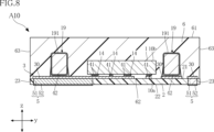
- FIG. 8 is a cross-sectional view taken along line VIII-VIII in FIG.
- FIG. 9 is a cross-sectional view taken along line IX-IX in FIG.
- FIG. 10 is a partially enlarged view of a part of FIG.
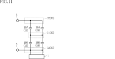
- FIG. 11 is a circuit diagram showing a part (two first electronic components and two second electronic components) of the electronic device according to the first embodiment.
- FIG. 12 is a circuit diagram equivalent to the circuit configuration shown in FIG.
- FIG. 13 is a cross-sectional view showing a step of the method for manufacturing the electronic device according to the first embodiment.
- FIG. 14 is a cross-sectional view showing a step of the method for manufacturing the electronic device according to the first embodiment.
- FIG. 15 is a cross-sectional view showing a step of the method for manufacturing the electronic device according to the first embodiment.
- FIG. 16 is a cross-sectional view showing a step of the method for manufacturing the electronic device according to the first embodiment.
- FIG. 17 is a cross-sectional view showing a step of the method for manufacturing the electronic device according to the first embodiment.
- FIG. 18 is a cross-sectional view showing a step of the method for manufacturing the electronic device according to the first embodiment.
- FIG. 19 is a cross-sectional view showing a step of the method for manufacturing the electronic device according to the first embodiment.
- FIG. 20 is a cross-sectional view showing a step of the method for manufacturing the electronic device according to the first embodiment.
- FIG. 21 is a cross-sectional view showing a step of the method for manufacturing the electronic device according to the first embodiment.
- FIG. 22 is a cross-sectional view showing a step of the method for manufacturing the electronic device according to the first embodiment.
- FIG. 23 is a cross-sectional view showing a step of the method for manufacturing the electronic device according to the first embodiment.
- FIG. 24 is an enlarged plan view of a main part showing an electronic device according to a first modified example of the first embodiment, and corresponds to FIG.
- FIG. 25 is a cross-sectional view showing an electronic device according to a second modified example of the first embodiment, and corresponds to the cross section of FIG.
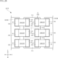
- FIG. 26 is a schematic diagram showing an electronic device according to a third modified example of the first embodiment.
- FIG. 27 is an enlarged plan view of a main part of an electronic device according to a second embodiment, and corresponds to FIG. FIG.
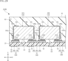
- FIG. 28 is a cross-sectional view showing an electronic device according to the second embodiment, and corresponds to the cross section of FIG.
- FIG. 29 is an enlarged cross-sectional view of a main part of an electronic device according to a second embodiment, and is an enlarged view of a part of FIG.
- FIG. 30 is an enlarged plan view of a main part showing an electronic device according to a modified example of the second embodiment, and corresponds to FIG.
- FIG. 31 is an enlarged cross-sectional view of a main part showing an electronic device according to a modified example of the second embodiment, and corresponds to the cross section of FIG.
- FIG. 32 is an enlarged plan view of a main part showing an electronic device according to a third embodiment, and corresponds to FIG. FIG.
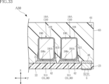
- FIG. 33 is an enlarged cross-sectional view of a main part showing an electronic device according to a third embodiment, and corresponds to the cross section of FIG.
- FIG. 34 is a schematic diagram showing an electronic device according to another embodiment.
- FIG. 35 is a cross-sectional view showing an electronic device according to another embodiment, which corresponds to the cross section of FIG.
- an object A is formed on an object B
- an object A is formed on (an object B)
- an object A is formed directly on an object B
- an object A is formed on an object B with another object interposed between the object A and the object B” unless otherwise specified.
- an object A is disposed on an object B” and “an object A is disposed on (an object B)” include “an object A is disposed directly on an object B” and “an object A is disposed on (an object B) with another object interposed between the object A and the object B” unless otherwise specified.
- an object A is located on (an object B) includes “an object A is in contact with an object B and is located on (an object B)” and “an object A is located on (an object B) with another object interposed between the object A and the object B".
- an object A overlaps an object B includes “an object A overlaps the entire object B” and “an object A overlaps a part of an object B” unless otherwise specified.
- an object A (its material) contains a certain material C includes “an object A (its material) is made of a certain material C” and “an object A (its material) is mainly composed of a certain material C.”
- a certain surface A faces a certain direction B (one side or the other side) includes, unless otherwise specified, the angle of surface A with respect to direction B is not limited to 90°, and includes the case where surface A is inclined with respect to direction B.
- a certain surface A is perpendicular to a certain surface B includes, unless otherwise specified, the angle of surface A with respect to surface B is not limited to 90°, and includes the case where surface A is inclined with respect to surface B.
- FIGS. 1 to 10 show an electronic device A10 according to a first embodiment.
- the electronic device A10 includes a semiconductor element 1, a plurality of electronic components 19, a support member 2, a wiring layer 3, a plurality of conductive bonding materials 41, 42, a plurality of external terminals 5, and a sealing resin 6.
- the thickness direction z is an example of the thickness direction of the electronic device A10.
- one side of the thickness direction z may be referred to as the upper side, and the other side as the lower side.
- the terms "upper”, “lower”, “upper”, “lower”, “top surface”, and “bottom surface” indicate the relative positional relationship of each component, etc. in the thickness direction z, and do not necessarily define the relationship with the direction of gravity.
- plane view refers to the case when viewed in the thickness direction z.
- Electronic device A10 is a device that is surface mounted on the wiring board of electronic devices, electric vehicles, and the like.
- Electronic device A10 is a leadless package type, and in particular, a QFN package (Quad Flat Non-leaded Package) type.
- Electronic device A10 is rectangular in plan view.
- the semiconductor element 1 is a component that is the core of the electronic device A10.
- the semiconductor element 1 is, for example, an integrated circuit such as an LSI. Unlike this example, the semiconductor element 1 may be a voltage control element such as an LDO (Low Drop Out), an amplification element such as an operational amplifier, or a discrete element such as a transistor or a diode.
- the semiconductor element 1 is rectangular in plan view.
- the semiconductor element 1 is supported by a support member 2.
- the semiconductor element 1 overlaps the support member 2 in plan view.
- the semiconductor element 1 has an element principal surface 10a and an element rear surface 10b.
- the element principal surface 10a and the element rear surface 10b are spaced apart in the thickness direction z.
- the element principal surface 10a and the element rear surface 10b face in opposite directions to each other.
- the element principal surface 10a faces the support member 2.
- the semiconductor element 1 has a plurality of electrode pads 14. Each of the plurality of electrode pads 14 is arranged on the element principal surface 10a. Each of the element's plurality of electrode pads 14 is electrically connected to an internal circuit (not shown) of the semiconductor element 1. Each of the plurality of electrode pads 14 is bonded to the wiring layer 3 via one of a plurality of conductive bonding materials 41. With this configuration, the semiconductor element 1 is bonded to the wiring layer 3 with the surface on which the plurality of electrode pads 14 are arranged (i.e., the element principal surface 10a) facing downward in the thickness direction z. In other words, the semiconductor element 1 is flip-chip mounted.
- the plurality of electronic components 19 are each supported by the support member 2 as shown in Figures 2, 6, 8 and 9.
- Each of the plurality of electronic components 19 is an SMD (Surface Mount Device).
- Each of the plurality of electronic components 19 is, for example, a resistor, a capacitor, or an inductor.
- the plurality of electronic components 19, together with the semiconductor element 1, are functional elements of the electronic device A10.
- the plurality of electronic components 19 are arranged around the semiconductor element 1 in a plan view.
- the multiple electronic components 19 include at least one first electronic component 19A and at least one second electronic component 19B, and in the illustrated example, include two first electronic components 19A and two second electronic components 19B.
- the two first electronic components 19A are electrically connected to each other in parallel.
- the two second electronic components 19B are electrically connected to each other in parallel.
- the two first electronic components 19A and the two second electronic components 19B are electrically connected in series.
- the performance of the two first electronic components 19A and the two second electronic components 19B with respect to each electrical characteristic is the same.
- the electrical characteristic is a resistance value when the electronic component 19 is a resistor, a capacitance when the electronic component 19 is a capacitor, and an inductance value when the electronic component 19 is an inductor. That is, in the electronic device A10, in an example where the two first electronic components 19A and the two second electronic components 19B are resistors, their resistance values are the same (or approximately the same), in an example where they are capacitors, their capacitances are the same (or approximately the same), and in an example where they are inductors, their inductance values are the same (or approximately the same). In a configuration different from the electronic device A10, the performance of the two first electronic components 19A and the two second electronic components 19B with respect to each electrical characteristic may be different from each other.
- the plurality of electronic components 19 includes a plurality of electronic components 19C and 19D, and in the illustrated example, includes two electronic components 19C and two electronic components 19D.
- the two electronic components 19C are electrically connected to each other in parallel.
- the two electronic components 19D are electrically connected to each other in parallel.
- the two electronic components 19C and the two electronic components 19D are electrically connected in series.
- the performance of each electrical characteristic of the two electronic components 19C and the two electronic components 19D is the same. In a configuration different from electronic device A10, the performance of each electrical characteristic of the two electronic components 19C and the two electronic components 19D may be different from each other.
- Each of the multiple electronic components 19 includes a main body 190 and a pair of terminals 191 and 192, as shown in Figures 2, 3, 6, 7, and 9.
- the main body 190 and the pair of terminals 191 and 192 described below are common to each of the electronic components 19 (including each of the first electronic components 19A, each of the second electronic components 19B, and each of the electronic components 19C and 19D), unless otherwise specified.
- the main body 190 is the functional center of the electronic component 19, and operates as a resistor, a capacitor, an inductor, or the like when electricity is applied to the electronic component 19. As shown in FIG. 3, the main body 190 is rectangular in plan view.
- the main body 190 has a pair of side surfaces 190a, 190b and a bottom surface 190c. As shown in FIG. 7, the pair of side surfaces 190a, 190b are spaced apart from each other in the longitudinal direction of each electronic component 19, and face opposite sides to each other in the longitudinal direction of each electronic component 19.
- the electronic components 19 include those whose orthogonal direction is the first direction x and those whose orthogonal direction is the second direction y, and among the electronic components 19, the longitudinal direction of each of the first electronic component 19A, each of the second electronic components 19B, and each of the electronic components 19C and 19D is the first direction x. As shown in FIG.
- the bottom surface 190c is connected to each of the pair of side surfaces 190a, 190b and is sandwiched between them.
- the bottom surface 190c faces downward in the thickness direction z and faces the support member 2.
- the main body 190 has a top surface facing upward in the thickness direction z, a side surface facing one side in the short side direction, and a side surface facing the other side in the short side direction.
- terminal 191, 192 are arranged on both sides of the main body 190 in the longitudinal direction.
- terminal 191 is arranged at one end in the longitudinal direction
- terminal 192 is arranged at the other end in the longitudinal direction.
- terminal 191 includes a lateral electrode 191a and a bottom electrode 191b.
- Side electrode 191a covers the entire side surface 190a.
- lateral electrode 191a connects from the upper (one) edge of side surface 190a in the thickness direction z to the lower (other) edge of side surface 190a in the thickness direction z.
- Bottom electrode 191b covers a portion of bottom surface 190c.
- Bottom electrode 191b covers the vicinity of one longitudinal edge of bottom surface 190c.
- Bottom electrode 191b is connected to lateral electrode 191a.
- terminal 191 includes a portion covering a portion of the top surface of main body 190, a portion of a side surface facing one side of main body 190 in the short direction, and a portion covering a portion of a side surface facing the other side of main body 190 in the short direction.
- the boundary between the side electrode 191a and the bottom electrode 191b is based on the bottom surface 190c, with the side electrode 191a on the upper side in the thickness direction z and the bottom electrode 191b on the lower side in the thickness direction z.
- the terminal 192 includes a lateral electrode 192a and a bottom electrode 192b.
- the lateral electrode 192a covers the entire side surface 190b.
- the lateral electrode 192a connects from the upper (one) edge of the side surface 190b in the thickness direction z to the lower (other) edge of the side surface 190b in the thickness direction z.
- the bottom electrode 192b covers a portion of the bottom surface 190c.
- the bottom electrode 192b covers the vicinity of the other longitudinal edge of the bottom surface 190c.
- the bottom electrode 192b is connected to the lateral electrode 192a.
- the terminal 192 includes a portion covering a portion of the top surface of the main body 190, a portion of a side surface facing one side of the main body 190 in the short direction, and a portion covering a portion of a side surface facing the other side of the main body 190 in the short direction.
- the boundary between the side electrode 192a and the bottom electrode 192b is based on the bottom surface 190c, with the side electrode 192a on the upper side in the thickness direction z and the bottom electrode 192b on the lower side in the thickness direction z.
- the support member 2 supports the semiconductor element 1 and a plurality of electronic components 19.
- the support member 2 includes, for example, a resin material.
- the resin material is, for example, the same as the sealing resin 6, but may be different from the sealing resin 6.
- the support member 2 may also include a filler such as silica mixed into the aforementioned resin material.
- the support member 2 may include a single crystal intrinsic semiconductor (for example, silicon (Si)) instead of a resin material.
- the support member 2 is rectangular in plan view.
- the thickness (dimension along the thickness direction z) of the support member 2 is not limited in any way, but is, for example, 30 ⁇ m or more and 200 ⁇ m or less.
- the support member 2 has a support surface 21, a back surface 22, and a plurality of side surfaces 23.
- the support surface 21 and the back surface 22 are spaced apart in the thickness direction z.
- the support surface 21 and the back surface 22 face opposite each other.
- the support surface 21 is the upper surface of the support member 2, and the back surface 22 is the lower surface of the support member 2.
- the support surface 21 faces the semiconductor element 1 (element main surface 10a).
- the back surface 22 faces the wiring board when the electronic device A10 is mounted on the wiring board.
- the support surface 21 is covered with the sealing resin 6, and the back surface 22 is exposed from the sealing resin 6.
- each of the multiple side surfaces 23 is sandwiched between the support surface 21 and the back surface 22.
- the upper end of each side surface 23 in the thickness direction z is connected to the support surface 21, and the lower end of each side surface 23 in the thickness direction z is connected to the back surface 22.
- Each side surface 23 is flat and perpendicular to each of the support surface 21 and the back surface 22.
- the wiring layer 3 is a conductor disposed inside the electronic device A10.
- the wiring layer 3 contains, for example, Cu.
- the wiring layer 3 is, for example, a laminate of a seed layer (containing, for example, titanium (Ti)) and a metal layer (containing, for example, Cu), but may be a single layer made of a conductor.
- the wiring layer 3 includes a plurality of wiring parts 30.
- the plurality of wiring parts 30 are spaced apart from each other.
- the plurality of wiring parts 30 include those that are conductive to the semiconductor element 1, those that are conductive to any of the plurality of electronic components 19, and those that are not conductive to either the semiconductor element 1 or the plurality of electronic components 19.
- the wiring layer 3 is formed on the support surface 21 and is in contact with the support surface 21.
- the thickness (dimension along the thickness direction z) of the wiring layer 3 is 3 ⁇ m or more and 100 ⁇ m or less.
- the multiple wiring portions 30 include a first wiring portion 31, a second wiring portion 32 and a third wiring portion 33.
- the first wiring portion 31, the second wiring portion 32 and the third wiring portion 33 are spaced apart from each other.
- the terminals 191 of the two first electronic components 19A are bonded to the first wiring portion 31 by conductive bonding material 42. As a result, the terminals 191 of the two first electronic components 19A are electrically connected via the first wiring portion 31.
- the terminals 192 of the two second electronic components 19B are bonded to the first wiring portion 31 by conductive bonding material 42. As a result, the terminals 192 of the two second electronic components 19B are electrically connected via the first wiring portion 31.
- the terminals 191 of the two first electronic components 19A and the terminals 192 of the two second electronic components 19B are electrically connected via the first wiring portion 31.
- the first wiring portion 31 is not electrically connected to either the semiconductor element 1 or the external terminals 5 without passing through either the two first electronic components 19A or the two second electronic components 19B.
- the first wiring portion 31 is electrically connected to the semiconductor element 1 and the external terminal 5 via either the two first electronic components 19A or the two second electronic components 19B.
- the first wiring portion 31 includes a plurality of partitions 311 and a connecting portion 312.
- the first wiring portion 31 includes two partitions 311.
- the two partitions 311 are spaced apart from each other.
- a terminal 191 of one of the two first electronic components 19A and a terminal 192 of one of the two second electronic components 19B are joined to one of the two partitions 311.
- a terminal 191 of the other of the two first electronic components 19A and a terminal 192 of the other of the two second electronic components 19B are joined to the other of the two partitions 311.
- the two partitions 311 are spaced apart in the second direction y.
- the connecting portion 312 is sandwiched between the two partitions 311.
- the connecting portion 312 is connected to each of the two partitions 311 and electrically connects the two partitions 311.
- the terminals 192 of the two first electronic components 19A are each joined to the second wiring portion 32 by a conductive bonding material 42. This allows the terminals 192 of the two first electronic components 19A to be electrically connected via the second wiring portion 32. In the example shown in Figures 2 to 4, the second wiring portion 32 is electrically connected to one of the multiple external terminals 5.
- the terminals 191 of the two second electronic components 19B are each joined to the third wiring portion 33 by a conductive bonding material 42. This allows the terminals 191 of the two second electronic components 19B to be electrically connected via the third wiring portion 33.
- the third wiring portion 33 is electrically connected to one of the multiple external terminals 5 and the semiconductor element 1.
- the first wiring portion 31, the second wiring portion 32, and the third wiring portion 33 are arranged along the first direction x.
- the first wiring portion 31 is located between the second wiring portion 32 and the third wiring portion 33 in the first direction x.
- the second wiring portion 32 is arranged on the other side of the first direction x relative to the first wiring portion 31, and the third wiring portion 33 is arranged on one side of the first direction x relative to the first wiring portion 31.
- the two first electronic components 19A are each arranged across the first wiring portion 31 and the second wiring portion 32.
- the two first electronic components 19A are arranged along the second direction y and overlap each other when viewed in the second direction y.
- the two second electronic components 19B are each arranged across the first wiring portion 31 and the third wiring portion 33.
- the two second electronic components 19B are arranged along the second direction y and overlap each other when viewed in the second direction y.
- the two first electronic components 19A and the two second electronic components 19B are arranged along the first direction x and overlap each other when viewed in the first direction x. Note that as long as the electrical connection relationship between the two first electronic components 19A and the two second electronic components 19B is the same, the arrangement of these components may be misaligned. For example, due to manufacturing errors, the two first electronic components 19A and the two second electronic components 19B may be misaligned.
- the multiple wiring parts 30 include multiple wiring parts 34, 35, and 36.
- the multiple wiring parts 34, 35, and 36 are spaced apart from each other.
- the terminals 191 of the two electronic components 19C are bonded to the wiring section 34 by conductive bonding material 42. As a result, the terminals 191 of the two electronic components 19C are electrically connected via the wiring section 34.
- the terminals 192 of the two electronic components 19D are bonded to the wiring section 34 by conductive bonding material 42. As a result, the terminals 192 of the two electronic components 19D are electrically connected via the wiring section 34.
- the terminals 191 of the two electronic components 19C and the terminals 192 of the two electronic components 19D are electrically connected via the wiring section 34. As shown in Figures 2 and 4, the wiring section 34 is not electrically connected to either the semiconductor element 1 or the external terminals 5 without passing through any of the multiple electronic components 19C, 19D.
- the wiring section 34 is electrically connected to the semiconductor element 1 and the external terminals 5 by passing through any of the multiple electronic components 19C, 19D. Although details are omitted, the wiring section 34 includes multiple partition sections and connecting sections, similar to the first wiring section 31.
- the terminals 192 of the two electronic components 19C are each joined to the wiring section 35 by a conductive bonding material 42. This allows the terminals 192 of the two electronic components 19C to be electrically connected via the wiring section 35. In the example shown in Figures 2 and 4, the wiring section 35 is electrically connected to the semiconductor element 1.
- the terminals 191 of the two electronic components 19D are each joined to the wiring portion 36 by a conductive bonding material 42. This allows the terminals 191 of the two electronic components 19D to be electrically connected via the wiring portion 36. In the example shown in Figures 2 and 4, the wiring portion 36 is electrically connected to the semiconductor element 1.
- the multiple wiring portions 34, 35, and 36 are arranged along the first direction x.
- Wiring portion 34 is located between wiring portion 35 and wiring portion 36 in the first direction x.
- Wiring portion 35 is arranged on the other side of wiring portion 34 in the first direction x, and wiring portion 36 is arranged on one side of wiring portion 34 in the first direction x.
- the two electronic components 19C are arranged across the wiring section 34 and the wiring section 35.
- the two electronic components 19C are arranged along the second direction y and overlap each other when viewed in the second direction y.
- the two electronic components 19D are arranged across the wiring section 34 and the wiring section 36.
- the two electronic components 19D are arranged along the second direction y and overlap each other when viewed in the second direction y.
- the two electronic components 19C and the two electronic components 19D are arranged along the first direction x and overlap each other individually when viewed in the first direction x. Note that the arrangement of the two electronic components 19C and the two electronic components 19D may be misaligned as long as the electrical connection relationship between the two electronic components 19C and the two electronic components 19D is the same. For example, the two electronic components 19C and the two electronic components 19D may be misaligned due to manufacturing errors.
- each of the multiple conductive bonding materials 41 bonds the wiring layer 3 to one of the multiple electrode pads 14 of the semiconductor element 1.
- the semiconductor element 1 is electrically connected to the wiring layer 3 via the multiple conductive bonding materials 41.
- Each of the multiple conductive bonding materials 41 is a conductive bonding material.
- the multiple conductive bonding materials 41 are, for example, solder.
- the solder contains an alloy (for example, an Sn-silver (Ag) alloy) that contains tin (Sn) in its composition, and contains flux.
- the composition of each of the multiple conductive bonding materials 41 is not limited to this example.
- the thickness (dimension along the thickness direction z) of each conductive bonding material 41 is not limited in any way, but is, for example, 15 ⁇ m to 100 ⁇ m.
- each of the multiple conductive bonding materials 42 bond the wiring layer 3 (any of the multiple wiring sections 30) to a corresponding one of the pairs of terminals 191, 192 of each of the multiple electronic components 19.
- Each of the multiple conductive bonding materials 42 is a conductive bonding material.
- Each conductive bonding material 42 is, for example, solder.
- the solder includes an alloy (for example, an Sn-silver (Ag) alloy) that contains tin (Sn) in its composition.
- Each conductive bonding material 42 may or may not contain flux.
- the thickness (dimension along the thickness direction z) of each conductive bonding material 42 is not limited in any way, but is, for example, 1 ⁇ m or more and 20 ⁇ m or less.
- each of the multiple conductive bonding materials 42 includes a fillet portion 421.
- the fillet portion 421 contacts either the lateral electrode 191a of the terminal 191 or the lateral electrode 192a of the terminal 192 of each electronic component 19.
- the side surface of the fillet portion 421 is convexly curved, but it may be concavely curved or may not be curved.
- Each of the external terminals 5 is electrically connected to the wiring layer 3 and is a conductor exposed to the outside of the electronic device A10.
- Each of the external terminals 5 serves as a terminal when the electronic device A10 is mounted on a wiring board. As shown in FIG. 6 and FIG. 8 to FIG. 10, each of the external terminals 5 penetrates the support member 2 in the thickness direction z.
- the external terminals 5 include those that are electrically connected to the semiconductor element 1 through the wiring layer 3, those that are electrically connected to one of the electronic components 19 and the semiconductor element 1 through the wiring layer 3, those that are electrically connected to one of the electronic components 19 through the wiring layer 3, and those that are not electrically connected to either the semiconductor element 1 or the electronic components 19.
- all of the external terminals 5 are disposed outside the semiconductor element 1 in a plan view and do not overlap either the semiconductor element 1 or the electronic components 19 in a plan view. Unlike this example, some of the external terminals 5 may overlap either the semiconductor element 1 or the electronic components 19 in a plan view.
- each of the multiple external terminals 5 includes a columnar portion 51 and an external electrode portion 52.
- the columnar portion 51 and external electrode portion 52 described below are common to each external terminal 5 unless otherwise specified.
- the columnar portion 51 penetrates the support member 2 in the thickness direction z.
- the columnar portion 51 includes, for example, a metal material.
- the metal material is not limited to any particular material, but is, for example, Cu.
- the planar shape of the columnar portion 51 is not limited to any particular material, but is rectangular or polygonal in the illustrated example.
- the upper surface of the columnar portion 51 (the surface facing upward in the thickness direction z) is, for example, flush with the support surface 21 of the support member 2.
- the upper surface of this columnar portion 51 contacts the wiring layer 3. Note that, among the multiple external terminals 5, there may be some whose upper surface is not in contact with the wiring layer 3. Such an external terminal 5 becomes a dummy terminal.
- the lower surface of the columnar portion 51 (the surface facing downward in the thickness direction z) is exposed from the support member 2.
- the lower surface of this columnar portion 51 is, for example, flush with the rear surface 22 of the support member 2.
- the side surface of the columnar portion 51 (the surface facing the first direction x or the second direction y) of all external terminals 5 is covered by the support member 2, but unlike this example, some external terminals 5 may have exposed side surfaces of the columnar portion 51.
- the external electrode portion 52 contacts the portion of the columnar portion 51 that is exposed from the back surface 22 of the support member 2.
- the external electrode portion 52 protrudes from the back surface 22.
- the external electrode portion 52 is formed by electroless plating.
- the external electrode portion 52 is composed of multiple metal layers, for example, a Ni layer, a palladium (Pd) layer, and a gold (Au) layer stacked in this order from the side in contact with the columnar portion 51.
- the external electrode portion 52 can also be composed of multiple metal layers, such as a Ni layer and an Au layer stacked in this order from the side in contact with the columnar portion 51, or multiple metal layers, such as a Cu layer, an Ag layer, and an Sn layer stacked in this order.
- the material and formation method of the external electrode portion 52 are not limited to these examples.
- the sealing resin 6 is a synthetic resin whose main component is, for example, a black epoxy resin.
- the sealing resin 6 may contain fillers such as silica mixed into the epoxy resin.
- the sealing resin 6 covers the semiconductor element 1, the electronic components 19, the wiring layer 3, and the like.
- the sealing resin 6 also covers a part of the support member 2, the conductive bonding materials 41, and the conductive bonding materials 42.
- the sealing resin 6 is formed on the support surface 21.
- the sealing resin 6 is rectangular in plan view. As shown in FIG. 1, FIG. 2, and FIG. 5 to FIG. 10, the sealing resin 6 has a resin main surface 61, a resin back surface 62, and multiple resin side surfaces 63.
- the resin main surface 61 and the resin back surface 62 are separated in the thickness direction z.
- the resin main surface 61 and the resin back surface 62 face opposite each other in the thickness direction z.
- the resin main surface 61 faces the same direction as the support surface 21 in the thickness direction z
- the resin back surface 62 faces the same direction as the back surface 22 in the thickness direction z.
- the resin back surface 62 is in contact with the support surface 21.
- the resin back surface 62 has projections and recesses according to the shape of the wiring layer 3.
- each of the multiple resin side surfaces 63 is sandwiched between the resin main surface 61 and the resin back surface 62 in the thickness direction z and is connected to them.
- the multiple resin side surfaces 63 are flush with a corresponding one of the multiple side surfaces 23.
- FIG. 11 shows the connection relationship between two first electronic components 19A and two second electronic components 19B, with each electronic component 19 being a capacitor.
- the circuit diagram shown in Fig. 11 shows the connection relationship described above in accordance with the structural examples shown in Figs. 1 to 10, and the circuit diagram shown in Fig. 12 shows an equivalent representation of the circuit diagram shown in Fig. 11.
- two first electronic components 19A are electrically connected in parallel between the first wiring portion 31 and the second wiring portion 32.
- Two second electronic components 19B are electrically connected in parallel between the first wiring portion 31 and the third wiring portion 33.
- the two first electronic components 19A and the two second electronic components 19B are connected in series via the first wiring portion 31.
- the electrical characteristics (capacitance) of the two first electronic components 19A and the two second electronic components 19B are combined and equivalently grouped as one electronic component 19X between the second wiring section 32 and the third wiring section 33.
- the electrical characteristics of the two first electronic components 19A and the two second electronic components 19B are equivalent to one circuit symbol (electronic component 19X) in the circuit diagram.
- Figures 13 to 23 are cross-sectional views showing a step in the method for manufacturing electronic device A10. These cross-sectional views correspond to the cross-section shown in Figure 6. Note that the cross-sectional views shown in Figures 22 and 23 are opposite in thickness direction z to the cross-sectional views shown in Figures 13 to 21.
- a support substrate 80 is prepared, and a plurality of columnar conductors 851 are formed on the support substrate 80.
- the support substrate 80 includes, for example, a single crystal intrinsic semiconductor material.
- the semiconductor material is, for example, Si.
- a silicon wafer is prepared as the support substrate 80.
- the support substrate 80 has a substrate main surface 80a and a substrate back surface 80b that face opposite each other in the thickness direction z.
- the plurality of columnar conductors 851 are formed, for example, by the following process.
- a seed layer is formed on the substrate main surface 80a.
- the seed layer is formed, for example, by a sputtering method.
- a resist is patterned on the seed layer, and a plurality of columnar conductors 851 are formed by electrolytic plating. After that, the resist layer and unnecessary seed layer are removed. Through these processes, a plurality of columnar conductors 851 are formed on the substrate main surface 80a of the support substrate 80.
- the columnar conductors 851 are portions that will later become the columnar portions 51 of the external terminals 5.
- a first resin layer 82 is formed on the substrate main surface 80a of the support substrate 80 to cover the columnar conductors 851.
- the first resin layer 82 is formed, for example, by molding.
- the first resin layer 82 is a synthetic resin whose main component is, for example, a black epoxy resin.
- the first resin layer 82 may be made of another insulating resin material instead of the synthetic resin.
- the first resin layer 82 has a main surface 821 and a bottom surface 822 that face opposite each other in the thickness direction z.
- the main surface 821 faces the same direction as the substrate main surface 80a, and the bottom surface 822 faces the substrate main surface 80a.
- the first resin layer 82 is a member that will later become the support member 2.
- the first resin layer 82 is ground.
- the first resin layer 82 is ground from the main surface 821 until the columnar conductors 851 are exposed from the main surface 821.
- the grinding method is not particularly limited.
- the first resin layer 82 may be made thinner by a method other than grinding.
- the columnar portions 51 are formed from the columnar conductors 851.
- the wiring layer 3 is formed, for example, by the following process.
- a seed layer is formed on the main surface 821 and each columnar portion 51.
- the seed layer is formed, for example, by a sputtering method.
- a Ti layer and a Cu layer are laminated in this order as the seed layer.
- a resist is patterned on the seed layer, and a metal layer is formed by electrolytic plating.
- the metal layer contains Cu.
- the resist and unnecessary seed layer seed layer exposed from the metal layer
- the wiring layer 3 is formed.
- a plurality of conductive bonding materials 420 are formed.
- a solder paste as each conductive bonding material 420 is formed on the corresponding wiring portion 30 (wiring layer 3) by screen printing. Note that the method of forming the plurality of conductive bonding materials 420 is not limited to this.
- the corresponding wiring portion 30 is one of the plurality of wiring portions 30 to which the plurality of electronic components 19 will be later bonded.
- a plurality of electronic components 19 are mounted, and then the plurality of electronic components 19 are bonded.
- the terminals 191 of the electronic components 19 and the conductive bonding materials 420 are placed in correspondence with each other.
- reflow is performed with each electronic component 19 placed.
- Each conductive bonding material 420 melts due to the heat from this reflow.
- the molten conductive bonding materials 420 are cooled, so that each conductive bonding material 420 solidifies and becomes each conductive bonding material 42.
- each electronic component 19 is bonded by each conductive bonding material 42.
- a fillet portion 421 is formed in each conductive bonding material 42 formed, as shown in Fig. 19.
- each conductive bonding material 410 formed on the semiconductor element 1 is placed in correspondence with the wiring layer 3 (any of the multiple wiring parts 30).
- the wiring layer 3 any of the multiple wiring parts 30.
- the corresponding wiring part 30 is one of the multiple wiring parts 30 to which the semiconductor element 1 is later bonded.
- flux is added to each conductive bonding material 410 formed on the semiconductor element 1.
- reflow is performed with the semiconductor element 1 placed.
- Each conductive bonding material 410 melts due to the heat from this reflow. Next, the melted conductive bonding material 410 is cooled, and each conductive bonding material 410 solidifies and becomes each conductive bonding material 41. This bonds the semiconductor element 1 with each conductive bonding material 41.
- a second resin layer 86 is formed.
- the second resin layer 86 is formed above the support member 2 so as to cover the semiconductor element 1, the electronic components 19, and the wiring layer 3.
- the second resin layer 86 is formed, for example, by molding.
- the second resin layer 86 is a synthetic resin whose main component is, for example, a black epoxy resin.
- the second resin layer 86 may be made of another insulating resin material instead of the synthetic resin.
- the second resin layer 86 is a member that will later become the sealing resin 6.
- the second resin layer 86 has a top surface 861 facing one side in the thickness direction z. The top surface 861 corresponds to the main resin surface 61 of the sealing resin 6.
- the support substrate 80 is removed.
- the support substrate 80 is ground from the rear surface 80b side of the substrate.
- the support substrate 80 is ground from the rear surface 80b side of the substrate.
- the grinding is continued even after the support substrate 80 is removed, thereby reducing the height of the support member 2 and the columnar portion 51. This reduction in height does not have to be performed.
- the external electrode portion 52 is formed.
- the external electrode portion 52 is formed on the top surface of the columnar portion 51 exposed from the back surface 22.
- the external electrode portion 52 is formed, for example, by electroless plating. In this electroless plating, a Ni layer, a Pd layer, and an Au layer are laminated in this order from the side in contact with the columnar portion 51. In this way, a plurality of external terminals 5 are formed, each of which includes a columnar portion 51 and an external electrode portion 52.
- the second resin layer 86 is cut along the cutting lines CL shown in FIG. 23 to separate the electronic device A10.
- the second resin layer 86 is cut by cutting using, for example, a dicing blade.
- the sealing resin 6 in the electronic device A10 is formed by dividing the second resin layer 86 along the cutting lines CL.
- the electronic device A10 shown in Figures 1 to 10 is manufactured.
- the manufacturing method of the electronic device A10 is not limited to the above example.
- the support member 2 contains a single crystal intrinsic semiconductor (e.g., Si)
- it is manufactured as follows. That is, a groove is formed in the support substrate 80 (silicon wafer) by etching or the like. Next, a plurality of columnar conductors 851 are formed in the groove. Next, the wiring layer 3 is formed without forming the first resin layer 82. Also, after the second resin layer 86 is formed, the support substrate 80 is not removed, but is ground until the plurality of columnar conductors 851 formed in the groove are exposed.
- a single crystal intrinsic semiconductor e.g., Si
- the wiring layer 3 includes a first wiring portion 31 to which one of a pair of terminals 191, 192 of each of the plurality of electronic components 19 is joined.
- the electrical characteristics of the plurality of electronic components 19 are equivalent to one circuit symbol in the circuit diagram.
- the electrical characteristics of one electronic component are designed as a composite value of the electrical characteristics of the plurality of electronic components 19 (two first electronic components 19A and two second electronic components 19B in this embodiment).
- various electrical characteristic values can be obtained by combining the plurality of electronic components 19, so that the electronic device A10 can design electrical specifications with high accuracy.
- the required electrical characteristics may be achieved by one electronic component 19X between the second wiring portion 32 and the third wiring portion 33.
- the size (for example, thickness) of the electronic component 19X becomes large.
- the thickness (dimension in the thickness direction z) of the sealing resin 6 becomes large, and the stress applied from the sealing resin 6 to the support member 2 may cause the support member 2 to warp.
- the electrical characteristics of one electronic component are designed as a composite value of the electrical characteristics of the multiple electronic components 19, so it is possible to replace one electronic component 19X with multiple electronic components 19 that are thinner (thicker) than the electronic component 19X.
- the electronic device A10 can be designed to reduce the thickness of the sealing resin 6. As described above, such a reduction in thickness is preferable in terms of reducing the warping of the support member 2. As a result, the electronic device A10 can increase the degree of freedom in module design.
- the wiring layer 3 includes a first wiring portion 31, a second wiring portion 32, and a third wiring portion 33.
- the multiple electronic components 19 include a first electronic component 19A and a second electronic component 19B.
- the first electronic component 19A has a pair of terminals 191, 192 bonded to the first wiring portion 31 and the second wiring portion 32, respectively
- the second electronic component 19B has a pair of terminals 191, 192 bonded to the first wiring portion 31 and the third wiring portion 33, respectively.
- the second wiring portion 32 and the third wiring portion 33 are electrically connected to the first electronic component 19A and the second electronic component 19B via the first wiring portion 31.
- the first wiring section 31 is electrically connected to the semiconductor element 1 or the external terminals 5 via one of the electronic components 19 (the two first electronic components 19A and the two second electronic components 19B). With this configuration, the first wiring section 31 is not directly connected to either the semiconductor element 1 or the external terminals 5. Therefore, in a configuration in which electrical connection between the second wiring section 32 and the third wiring section 33 can be established by one electronic component, the first wiring section 31 can be provided to establish electrical connection between the second wiring section 32 and the third wiring section 33 by a series circuit of at least two electronic components 19 (one first electronic component 19A and one second electronic component 19B). In other words, electrical characteristics equivalent to one circuit symbol can be designed with multiple electronic components 19 between the second wiring section 32 and the third wiring section 33. This is preferable in terms of increasing the degree of freedom in the module design of the electronic device A10.
- the first wiring section 31 includes two partition sections 311 and a connecting section 312.
- the connecting section 312 connects the two partition sections 311 that are spaced apart from each other.
- the first wiring portion 31 is rectangular in plan view.
- the two first electronic components 19A overlap each other when viewed in the first direction x, and the two second electronic components 19B overlap each other when viewed in the first direction x. Furthermore, the two first electronic components 19A overlap each of the two second electronic components 19B individually when viewed in the second direction y.
- the distance difference is the distance difference between the conductive path in the first wiring portion 31 between the terminals 191 of the two first electronic components 19A and the conductive path in the first wiring portion 31 between the terminals 192 of the two second electronic components 19B.
- the distance difference is the distance difference between the conductive path in the first wiring part 31 between the terminal 191 included in one of the two first electronic components 19A and the terminal 192 included in one of the two second electronic components 19B, and the conductive path in the first wiring part 31 between the terminal 191 included in the other of the two first electronic components 19A and the terminal 192 included in the other of the two second electronic components 19B.
- This makes it possible to suppress the difference in the conductive path in the first wiring part 31 between the two first electronic components 19A and the two second electronic components 19B, thereby suppressing the electrical variation between the two first electronic components 19A and the two second electronic components 19B.
- the performance of each of the multiple electronic components 19 in terms of electrical characteristics is the same.
- this configuration for example, it is possible to equalize the sizes (thickness and planar size) of the multiple electronic components 19 (first electronic component 19A and second electronic component 19B), thereby suppressing variation in the thickness of each of the multiple electronic components 19.
- This makes it easier for electronic device A10 to design the thickness (dimension in thickness direction z) of sealing resin 6.
- electronic device A10 makes it easier to calculate the composite component of the electrical characteristics of the multiple electronic components 19.
- support member 2 contains a resin material, which is the same as sealing resin 6. With this configuration, the difference between the linear expansion coefficient of support member 2 and the linear expansion coefficient of sealing resin 6 can be reduced, thereby suppressing thermal stress generated in electronic device A10.
- wiring layer 3 includes multiple wiring sections 34, 35, 36.
- Multiple electronic components 19 include multiple electronic components 19C, 19D.
- the relative positional relationship and electrical connection relationship between multiple wiring sections 34, 35, 36 and multiple electronic components 19C, 19D is similar to the relative positional relationship and electrical connection relationship between first wiring section 31, second wiring section 32, and third wiring section 33, and at least one first electronic component 19A and at least one second electronic component 19B. Therefore, these actions and effects are common.
- FIG. 24 shows an electronic device A11 according to a first modified example of the first embodiment.
- the electronic device A11 differs from the electronic device A10 in the following respects.
- First, each terminal 191 of the two first electronic components 19A and each terminal 192 of the two second electronic components 19B are joined to the first wiring portion 31 by one conductive bonding material 42.
- Second, each terminal 192 of the two first electronic components 19A are joined to the second wiring portion 32 by one conductive bonding material 42.
- each terminal 191 of the two second electronic components 19B are joined to the third wiring portion 33 by one conductive bonding material 42.
- each first electronic component 19A and each second electronic component 19B are joined to the first wiring portion 31 by one conductive bonding material 42.
- each first electronic component 19A and each second electronic component 19B is not limited to a configuration in which they are individually joined to the first wiring portion 31, but includes a configuration in which they are joined collectively to the first wiring portion 31.
- two first electronic components 19A are joined to the second wiring portion 32 by one conductive bonding material 42.
- two first electronic components 19A are not limited to a configuration in which they are individually joined to the second wiring portion 32, but includes a configuration in which they are joined collectively to the second wiring portion 32.
- two second electronic components 19B are joined to the third wiring portion 33 by one conductive bonding material 42.
- the two second electronic components 19B are not limited to a configuration in which they are each individually joined to the third wiring portion 33, but also include a configuration in which they are collectively joined to the third wiring portion 33.
- FIG. 25 shows an electronic device A12 according to a second modified example of the first embodiment.
- the electronic device A12 differs from the electronic device A10 in the following respect. That is, the thickness (dimension in the thickness direction z) of the semiconductor element 1 of the electronic device A12 is greater than the thickness of the semiconductor element 1 of the electronic device A10.
- each electronic component 19 is made low-profile. Even after each electronic component 19 is made low-profile, if there is a difference between the thickness (dimension in thickness direction z) of each electronic component 19 and the thickness (dimension in thickness direction z) of the semiconductor element 1, the thickness of the semiconductor element 1 may be made as thick as the thickness of each electronic component 19. Increasing the volume of the semiconductor element 1 in this way makes it possible to reduce the volume (formation amount) of the sealing resin 6. This reduces the volume (formation amount) of the sealing resin 6, thereby suppressing the stress applied from the sealing resin 6 to the support member 2. For this reason, electronic device A12 can reduce warping of support member 2 more than electronic device A10.
- FIG. 26 shows an electronic device A13 according to a third modified example of the first embodiment.
- the electronic device A13 differs from the electronic device A10 in the following respects.
- the plurality of electronic components 19 includes three first electronic components 19A.
- the plurality of electronic components 19 includes three second electronic components 19B.
- first electronic components 19A are electrically connected in parallel, and three second electronic components 19B are electrically connected in parallel.
- the three first electronic components 19A and the three second electronic components 19B are electrically connected in series.
- the number of first electronic components 19A and the number of second electronic components 19B are not limited in any way. Note that, although the number of first electronic components 19A and the number of second electronic components 19B are the same in each of electronic devices A10 and A13, they may be different.
- Each of the electronic devices A11 to A13 like the electronic device A10, includes a first wiring section 31 to which one of a pair of terminals 191, 192 of each of the multiple electronic components 19 (at least one first electronic component 19A and at least one second electronic component 19B) is joined, and the electrical characteristics of the multiple electronic components 19 are equivalent to one circuit symbol in the circuit diagram. Therefore, like the electronic device A10, each of the electronic devices A11 to A13 can be designed with high-precision electrical specifications and a thin design, which increases the freedom of module design. Additionally, each of the electronic devices A11 to A13 has the same effects as the electronic device A10 due to the configuration they share in common.
- FIGS. 27 to 29 show an electronic device A20 according to the second embodiment.
- Electronic device A20 differs from electronic device A10 in the following respect. That is, the first wiring portion 31, the second wiring portion 32, and the third wiring portion 33 each include a main body portion 301 and multiple base portions 302.
- the main body 301 includes a seed layer (containing, for example, titanium (Ti)) and a metal layer (containing, for example, Cu).
- the base 302 is laminated on the main body 301.
- the base 302 is disposed in a portion where each electronic component 19 is bonded, and is disposed between the main body 301 and the corresponding conductive bonding material 42.
- Each base 302 includes the same metal (for example, Cu) as the metal layer of the main body 301.
- each base 302 may include a metal (for example, nickel) different from the metal layer of the main body 301.
- the base 302 functions as a barrier metal and can suppress the conductive bonding material 42 from penetrating into the wiring layer 3 (the metal layer of the main body 301).
- the first wiring portion 31 includes a plurality of bonding surfaces 31a and a recess 31b.
- each bonding surface 31a is indicated by a dot.
- Each of the plurality of bonding surfaces 31a is a surface of the first wiring portion 31 that contacts a corresponding conductive bonding material 42.
- four conductive bonding materials 42 are arranged on the first wiring portion 31, and therefore the first wiring portion 31 includes four bonding surfaces 31a.
- Each bonding surface 31a corresponds individually to the upper surfaces of the plurality of base portions 302 in the first wiring portion 31.
- the recess 31b is a portion recessed from the plurality of bonding surfaces 31a toward the support surface 21 of the support member 2 in the thickness direction z. In this embodiment, the recess 31b is located between adjacent ones of the plurality of bonding surfaces 31a in a plan view. In the illustrated example, the recess 31b has a linear portion extending in the first direction x in a plan view and a linear portion extending in the second direction y in a plan view, which intersect at the center of the first wiring portion 31.
- the first wiring portion 31 includes a main body portion 301 and a plurality of base portions 302, so that, as shown in FIG.
- the portions of the first wiring portion 31 to which the electronic components 19 are bonded are partially elevated.
- a recess 31b is formed in the first wiring portion 31.
- the second wiring portion 32 and the third wiring portion 33 each include a main body portion 301 and a plurality of base portions 302, and therefore include a plurality of bonding surfaces and recesses similar to the plurality of bonding surfaces 31a and recesses 31b of the first wiring portion 31.
- base portion 302 is also formed in the bonding region of semiconductor element 1. Unlike this example, base portion 302 does not have to be formed in the bonding region of semiconductor element 1. Also, base portion 302 only needs to be formed in at least each bonding region of two first electronic components 19A and two second electronic components 19B, and does not have to be formed in the bonding regions of other electronic components 19.
- a first wiring section 31 is included to which one of a pair of terminals 191, 192 of each of a plurality of electronic components 19 (at least one first electronic component 19A and at least one second electronic component 19B) is joined, and the electrical characteristics of the plurality of electronic components 19 are equivalent to one circuit symbol in the circuit diagram. Therefore, like electronic device A10, electronic device A20 allows for the design of highly accurate electrical specifications and a design that aims for a thin design, thereby increasing the freedom of module design. In addition, electronic device A20 has a common configuration with electronic device A10 and thereby achieves the same effects as electronic device A10.
- recesses 31b are disposed between multiple bonding surfaces 31a. With this configuration, a step is created between each bonding surface 31a and the recesses 31b. This step can prevent the conductive bonding material 42 from spreading wet along the wiring layer 3. As a result, the outflow of the conductive bonding material 42 is prevented, and an insufficient thickness of the conductive bonding material 42 and tilting of the posture of each electronic component 19 can be prevented. In other words, the electronic device A20 can prevent poor bonding of the electronic components 19 and reduce deterioration of reliability.
- FIGS. 30 and 31 show an electronic device A21 according to a first modified example of the second embodiment.
- the electronic device A21 is different from the electronic device A20 in that the first wiring portion 31, the second wiring portion 32, and the third wiring portion 33 each include a main body portion 301 and a groove portion 303.
- each groove portion 303 extends in the first direction x or the second direction y in a plan view.
- multiple groove portions 303 may be arranged intermittently along the first direction x or the second direction y.
- the first wiring portion 31 of the electronic device A21 includes a plurality of bonding surfaces 31a and recesses 31b.
- each bonding surface 31a is indicated by a dot.
- the recesses 31b are located between adjacent ones of the plurality of bonding surfaces 31a.
- the recesses 31b have a linear portion extending in the first direction x in plan view and a linear portion extending in the second direction y in plan view, which intersect at the center of the first wiring portion 31. Of these, the linear portion of the recesses 31b extending in the first direction x is formed in the connecting portion 312.
- the first wiring portion 31 includes a main body portion 301 and a groove portion 303, and as shown in FIG. 31, a portion of the first wiring portion 31 is recessed between the portions where the electronic components 19 are bonded (portions in contact with the conductive bonding material 42). As a result, a recess 31b is formed in the first wiring portion 31. That is, in the electronic device A21, the recess 31b corresponds to the groove portion 303.
- the first wiring portion 31 includes multiple recesses 31b arranged along the first direction x or the second direction y.
- the second wiring portion 32 and the third wiring portion 33 each include a main body portion 301 and a groove portion 303, and therefore include multiple bonding surfaces and recesses similar to the multiple bonding surfaces 31a and recesses 31b of the first wiring portion 31.
- a first wiring portion 31 is included to which one of a pair of terminals 191, 192 of each of a plurality of electronic components 19 (at least one first electronic component 19A and at least one second electronic component 19B) is joined, and the electrical characteristics of the plurality of electronic components 19 are equivalent to one circuit symbol in the circuit diagram.
- the plurality of electronic components 19 are two first electronic components 19A and two second electronic components 19B. Therefore, like the electronic device A10, the electronic device A20 can be designed to have high-precision electrical specifications and to be thin, which increases the freedom of module design.
- the electronic device A21 has a configuration in common with the electronic device A20, and thus achieves the same effects as the electronic device A20.
- electronic device A21 similar to electronic device A20, recesses 31b are arranged between multiple bonding surfaces 31a. Therefore, similar to electronic device A20, electronic device A21 can suppress tilting of the posture of each electronic component 19. Note that, unlike electronic device A20, electronic device A21 has grooves 303 formed in main body 301 in each of first wiring portion 31, second wiring portion 32, and third wiring portion 33, thereby providing each bonding surface 31a and recesses 31b.
- FIGS. 32 and 33 show an electronic device A30 according to a third embodiment.
- the electronic device A30 differs from the electronic device A10 in the following respect. That is, the first wiring section 31 of the electronic device A30 has two partition sections 311 that are separated from each other.
- the first wiring section 31 does not include a connecting section 312. This separates the two partition sections 311 from each other.
- one of the two first electronic components 19A and one of the two second electronic components 19B are electrically connected in series via one of the two partition sections 311.
- the other of the two first electronic components 19A and the other of the two second electronic components 19B are electrically connected in series via the other of the two partition sections 311.
- the series circuits, each including one first electronic component 19A and one second electronic component 19B are electrically connected in parallel.
- a first wiring section 31 is included to which one of a pair of terminals 191, 192 of each of a plurality of electronic components 19 (at least one first electronic component 19A and at least one second electronic component 19B) is joined, and the electrical characteristics of the plurality of electronic components 19 are equivalent to one circuit symbol in the circuit diagram. Therefore, like electronic device A10, electronic device A30 allows for the design of highly accurate electrical specifications and a design that aims for a thin design, thereby increasing the freedom of module design. In addition, electronic device A30 has a common configuration with electronic device A10 and thereby achieves the same effects as electronic device A10.
- the first wiring portion 31, the second wiring portion 32, and the third wiring portion 33 do not have to be arranged along a direction (e.g., the first direction x) perpendicular to the thickness direction z.
- Figure 34 shows an example of the arrangement of the first wiring portion 31, the second wiring portion 32, and the third wiring portion 33 according to such a modified example.
- the first wiring portion 31 is arranged on one side of each of the second wiring portion 32 and the third wiring portion 33 in the second direction y.
- the second wiring portion 32 and the third wiring portion 33 are arranged along the first direction x.
- the two first electronic components 19A are each arranged with their longitudinal direction aligned along the second direction y, and are joined across the first wiring portion 31 and the second wiring portion 32.
- the two second electronic components 19B are each arranged with their longitudinal direction aligned along the second direction y, and are joined across the first wiring portion 31 and the third wiring portion 33.
- the two first electronic components 19A and the two second electronic components 19B are arranged along the first direction x. In the example shown in FIG.
- the two first electronic components 19A and the two second electronic components 19B are aligned in the first direction x without any disturbance, but as long as the electrical connection relationship between the two first electronic components 19A and the two second electronic components 19B is the same, their arrangements may be misaligned. For example, due to manufacturing errors, the two first electronic components 19A and the two second electronic components 19B may be misaligned.
- the sealing resin 6 may have a step on each resin side surface 63.
- FIG. 35 shows an example of such a modification of an electronic device, which is applied to the electronic device A10 according to the first embodiment.
- FIG. 35 shows an example of application to the electronic device A10 according to the first embodiment, it is also possible to apply it to electronic devices according to other embodiments.
- each resin side surface 63 has a first side portion 631 and a second side portion 632.
- the first side portion 631 and the second side portion 632 face the same direction.
- the first side portion 631 is positioned outward from the second side portion 632 in a planar view.
- the first side portion 631 is connected to the resin main surface 61, and the second side portion 632 is connected to a corresponding one of the multiple side surfaces 23.
- the second side portion 632 is flush with the side surface 23 to which it is connected.
- each resin side surface 63 has a step.
- the multiple external terminals 5 include those in which the columnar portion 51 is exposed from the side surface 23.
- the external electrode portion 52 covers the surface of the columnar portion 51 exposed from the rear surface 22 of the support member 2 and the surface exposed from the side surface 23 of the support member 2.
- the electronic device shown in FIG. 35 also has the same effect as electronic device A10. Furthermore, in the electronic device shown in FIG. 35, in some of the multiple external terminals 5, the external electrode portion 52 is also formed on the surface of the columnar portion 51 that is exposed from the side surface 23. With this configuration, when the electronic device shown in FIG. 35 is mounted on a wiring board of an electronic device or the like, a fillet can be formed in the conductive bonding material (e.g., solder) used during the mounting. Therefore, the electronic device shown in FIG. 35 can easily be visually inspected to see if it is properly joined to the wiring board of an electronic device or the like.
- the conductive bonding material e.g., solder
- the second wiring section 32 and the third wiring section 33 are electrically connected through the plurality of electronic components 19 (at least one first electronic component 19A and at least one second electronic component 19B) and the first wiring section 31.
- the electronic device of the present disclosure may be configured such that the two wiring sections 30 are electrically connected only through the plurality of electronic components 19. Even in this case, the plurality of electronic components 19 are electrically connected so that their electrical characteristics are equivalent to one circuit symbol in the circuit diagram.
- two electronic components 19 arranged on one side of the support member 2 in the first direction x and arranged in the center in the second direction y are joined across two wiring sections 30.
- the two wiring sections 30 are electrically connected through the two electronic components 19.
- the number and arrangement of the semiconductor elements 1 and electronic components 19, the pattern of the wiring layer 3 (the number and arrangement of the multiple wiring sections 30), and the number and arrangement of the external terminals 5 are not limited to the examples shown in the figures.
- the planar layout of the electronic device of the present disclosure can be applied in various forms depending on the specifications of the electronic device.
- the electronic device disclosed herein is not limited to a configuration having a semiconductor element 1 as a functional element, but may have at least a plurality of electronic components 19.
- the electronic device according to the present disclosure is not limited to the above-described embodiment.
- the specific configuration of each part of the electronic device according to the present disclosure can be freely designed in various ways.
- the electronic device according to the present disclosure includes the embodiments described in the following appendix.
- Appendix 1 A plurality of electronic components each including a pair of terminals; a support member having a support surface for supporting the plurality of electronic components; A wiring layer formed on the support surface; a sealing resin for covering each of the plurality of electronic components; Equipped with the wiring layer includes a first wiring portion to which one of the pair of terminals of each of the plurality of electronic components is joined, An electronic device, wherein the electrical characteristics of the plurality of electronic components are represented by a single circuit symbol in a circuit diagram.
- the wiring layer includes a second wiring portion and a third wiring portion spaced apart from each other and from the first wiring portion; each of the plurality of electronic components is electrically connected between the second wiring portion and the third wiring portion;
- the electronic device described in Appendix 1 wherein the plurality of electronic components include at least one first electronic component having the pair of terminals joined to the first wiring portion and the second wiring portion, respectively, and at least one second electronic component having the pair of terminals joined to the first wiring portion and the third wiring portion, respectively.
- Appendix 3 The at least one first electronic component includes two first electronic components, the at least one second electronic component includes two second electronic components; 3.
- the electronic device of claim 2 wherein the two first electronic components and the two second electronic components are electrically connected in series with each other.
- Each of the plurality of electronic components includes a main body portion, The support surface faces one side in a thickness direction of the support member, 4.
- Appendix 5. the first wiring portion, the second wiring portion, and the third wiring portion are arranged along the first direction, 5.
- the electronic device of claim 4 wherein the first wiring portion is located between the second wiring portion and the third wiring portion.
- the first wiring portion includes two partition portions spaced apart from each other, one of the two first electronic components and one of the two second electronic components are joined to one of the two partitions;
- Appendix 7. The electronic device according to claim 6, wherein the first wiring portion includes a connecting portion that is sandwiched between the two partitions and connects the two partitions.
- Appendix 8. the two first electronic components overlap each other when viewed in the first direction, the two second electronic components overlap each other when viewed in the first direction; 8.
- the electronic device wherein the two first electronic components overlap the two second electronic components individually when viewed in the thickness direction and in a second direction perpendicular to the first direction.
- Appendix 9. Further comprising a plurality of external terminals; The support member has a back surface facing the opposite side to the support surface in a thickness direction of the support member, the plurality of external terminals are exposed on the back surface, 9.
- the electronic device according to claim 1, wherein the plurality of conductive bonding materials individually bond the first wiring portion to one of the pair of terminals of each of the plurality of electronic components.
- the first wiring portion has a plurality of bonding surfaces that are in contact with the plurality of conductive bonding materials, respectively, and at least one recess that is recessed from the plurality of bonding surfaces toward the support surface in a thickness direction of the support member, 11.
- the electronic device of claim 10 wherein the at least one recess is located between adjacent ones of the plurality of bonding surfaces when viewed in the thickness direction.
- Appendix 12. 12. The electronic device according to claim 1, wherein the performance of each of the plurality of electronic components with respect to the electrical characteristics is the same as each other.
- Appendix 13 13.
- the electronic device of claim 12, wherein the electrical characteristic is one of a capacitance, a resistance value, and an inductance value.
- Appendix 14. Further comprising a semiconductor element, 14.
- Appendix 15. The electronic device of claim 14, wherein the plurality of electronic components are arranged around the semiconductor element when viewed in a thickness direction of the support member.
- Appendix 16. 16. The electronic device according to claim 14, wherein the sealing resin covers the semiconductor element as well as the plurality of electronic components.
- Appendix 17. The electronic device according to claim 1, wherein the support member includes an insulating resin material. Appendix 18. 18. The electronic device according to claim 17, wherein the support member contains the same resin material as the sealing resin.
Landscapes
- Engineering & Computer Science (AREA)
- Microelectronics & Electronic Packaging (AREA)
- Power Engineering (AREA)
- Manufacturing & Machinery (AREA)
- Structures Or Materials For Encapsulating Or Coating Semiconductor Devices Or Solid State Devices (AREA)
- Structures For Mounting Electric Components On Printed Circuit Boards (AREA)
Priority Applications (2)
| Application Number | Priority Date | Filing Date | Title |
|---|---|---|---|
| JP2025527621A JPWO2024262253A1 (https=) | 2023-06-21 | 2024-05-27 | |
| US19/421,925 US20260107377A1 (en) | 2023-06-21 | 2025-12-16 | Electronic device |
Applications Claiming Priority (2)
| Application Number | Priority Date | Filing Date | Title |
|---|---|---|---|
| JP2023-101351 | 2023-06-21 | ||
| JP2023101351 | 2023-06-21 |
Related Child Applications (1)
| Application Number | Title | Priority Date | Filing Date |
|---|---|---|---|
| US19/421,925 Continuation US20260107377A1 (en) | 2023-06-21 | 2025-12-16 | Electronic device |
Publications (1)
| Publication Number | Publication Date |
|---|---|
| WO2024262253A1 true WO2024262253A1 (ja) | 2024-12-26 |
Family
ID=93935499
Family Applications (1)
| Application Number | Title | Priority Date | Filing Date |
|---|---|---|---|
| PCT/JP2024/019376 Ceased WO2024262253A1 (ja) | 2023-06-21 | 2024-05-27 | 電子装置 |
Country Status (3)
| Country | Link |
|---|---|
| US (1) | US20260107377A1 (https=) |
| JP (1) | JPWO2024262253A1 (https=) |
| WO (1) | WO2024262253A1 (https=) |
Citations (4)
| Publication number | Priority date | Publication date | Assignee | Title |
|---|---|---|---|---|
| JPS63117454A (ja) * | 1986-11-06 | 1988-05-21 | Fujitsu Ltd | 混成集積回路 |
| JPH0917914A (ja) * | 1995-06-29 | 1997-01-17 | Toshiba Corp | 半導体装置 |
| JP2005101609A (ja) * | 2003-09-23 | 2005-04-14 | Samsung Electronics Co Ltd | オンチップバイパスキャパシタの製造方法及びチップ |
| JP2014093360A (ja) * | 2012-11-01 | 2014-05-19 | Toyota Industries Corp | 基板 |
-
2024
- 2024-05-27 JP JP2025527621A patent/JPWO2024262253A1/ja active Pending
- 2024-05-27 WO PCT/JP2024/019376 patent/WO2024262253A1/ja not_active Ceased
-
2025
- 2025-12-16 US US19/421,925 patent/US20260107377A1/en active Pending
Patent Citations (4)
| Publication number | Priority date | Publication date | Assignee | Title |
|---|---|---|---|---|
| JPS63117454A (ja) * | 1986-11-06 | 1988-05-21 | Fujitsu Ltd | 混成集積回路 |
| JPH0917914A (ja) * | 1995-06-29 | 1997-01-17 | Toshiba Corp | 半導体装置 |
| JP2005101609A (ja) * | 2003-09-23 | 2005-04-14 | Samsung Electronics Co Ltd | オンチップバイパスキャパシタの製造方法及びチップ |
| JP2014093360A (ja) * | 2012-11-01 | 2014-05-19 | Toyota Industries Corp | 基板 |
Also Published As
| Publication number | Publication date |
|---|---|
| JPWO2024262253A1 (https=) | 2024-12-26 |
| US20260107377A1 (en) | 2026-04-16 |
Similar Documents
| Publication | Publication Date | Title |
|---|---|---|
| JP4606849B2 (ja) | デカップリングコンデンサを有する半導体チップパッケージ及びその製造方法 | |
| US7049692B2 (en) | Stacked semiconductor device | |
| US7573722B2 (en) | Electronic carrier board applicable to surface mounted technology (SMT) | |
| JP2011040602A (ja) | 電子装置およびその製造方法 | |
| KR100606295B1 (ko) | 회로 모듈 | |
| KR100711675B1 (ko) | 반도체 장치 및 그 제조 방법 | |
| US20060055018A1 (en) | Semiconductor device | |
| CN112018063B (zh) | 半导体封装、半导体装置及半导体封装的制造方法 | |
| US20130020572A1 (en) | Cap Chip and Reroute Layer for Stacked Microelectronic Module | |
| KR102481099B1 (ko) | 복합 반도체 패키지 제조방법 | |
| US20050224934A1 (en) | Circuit device | |
| WO2024262253A1 (ja) | 電子装置 | |
| JP3926736B2 (ja) | 配線基板及びその製造方法並びに半導体装置 | |
| JP5178028B2 (ja) | 半導体装置の製造方法 | |
| JP7022541B2 (ja) | 半導体装置 | |
| JP2005057271A (ja) | 同一平面上に横配置された機能部及び実装部を具備する半導体チップパッケージ及びその積層モジュール | |
| JP7382167B2 (ja) | 電子装置、および電子装置の製造方法 | |
| WO2024262239A1 (ja) | 電子装置 | |
| JP2012080145A (ja) | 半導体装置 | |
| US20260005157A1 (en) | Electronic device | |
| US20250318053A1 (en) | Electronic device and method for manufacturing electronic device | |
| JP2024051292A (ja) | 半導体装置 | |
| US20260107814A1 (en) | Electronic device | |
| JP4296916B2 (ja) | 半導体装置 | |
| WO2024209917A1 (ja) | 電子装置 |
Legal Events
| Date | Code | Title | Description |
|---|---|---|---|
| 121 | Ep: the epo has been informed by wipo that ep was designated in this application |
Ref document number: 24825660 Country of ref document: EP Kind code of ref document: A1 |
|
| ENP | Entry into the national phase |
Ref document number: 2025527621 Country of ref document: JP Kind code of ref document: A |
|
| WWE | Wipo information: entry into national phase |
Ref document number: 2025527621 Country of ref document: JP |
|
| NENP | Non-entry into the national phase |
Ref country code: DE |