WO2024257835A1 - 金属と絶縁体との接合体、その用途、および金属と絶縁体との接合体の製造方法 - Google Patents
金属と絶縁体との接合体、その用途、および金属と絶縁体との接合体の製造方法 Download PDFInfo
- Publication number
- WO2024257835A1 WO2024257835A1 PCT/JP2024/021572 JP2024021572W WO2024257835A1 WO 2024257835 A1 WO2024257835 A1 WO 2024257835A1 JP 2024021572 W JP2024021572 W JP 2024021572W WO 2024257835 A1 WO2024257835 A1 WO 2024257835A1
- Authority
- WO
- WIPO (PCT)
- Prior art keywords
- metal
- metal member
- joint
- insulating member
- grain size
- Prior art date
- Legal status (The legal status is an assumption and is not a legal conclusion. Google has not performed a legal analysis and makes no representation as to the accuracy of the status listed.)
- Ceased
Links
Images






Classifications
-
- C—CHEMISTRY; METALLURGY
- C04—CEMENTS; CONCRETE; ARTIFICIAL STONE; CERAMICS; REFRACTORIES
- C04B—LIME, MAGNESIA; SLAG; CEMENTS; COMPOSITIONS THEREOF, e.g. MORTARS, CONCRETE OR LIKE BUILDING MATERIALS; ARTIFICIAL STONE; CERAMICS; REFRACTORIES; TREATMENT OF NATURAL STONE
- C04B37/00—Joining burned ceramic articles with other burned ceramic articles or other articles by heating
- C04B37/02—Joining burned ceramic articles with other burned ceramic articles or other articles by heating with metallic articles
- C04B37/023—Joining burned ceramic articles with other burned ceramic articles or other articles by heating with metallic articles characterised by the interlayer used
- C04B37/025—Joining burned ceramic articles with other burned ceramic articles or other articles by heating with metallic articles characterised by the interlayer used consisting of glass or ceramic material
-
- C—CHEMISTRY; METALLURGY
- C04—CEMENTS; CONCRETE; ARTIFICIAL STONE; CERAMICS; REFRACTORIES
- C04B—LIME, MAGNESIA; SLAG; CEMENTS; COMPOSITIONS THEREOF, e.g. MORTARS, CONCRETE OR LIKE BUILDING MATERIALS; ARTIFICIAL STONE; CERAMICS; REFRACTORIES; TREATMENT OF NATURAL STONE
- C04B37/00—Joining burned ceramic articles with other burned ceramic articles or other articles by heating
- C04B37/02—Joining burned ceramic articles with other burned ceramic articles or other articles by heating with metallic articles
- C04B37/023—Joining burned ceramic articles with other burned ceramic articles or other articles by heating with metallic articles characterised by the interlayer used
- C04B37/026—Joining burned ceramic articles with other burned ceramic articles or other articles by heating with metallic articles characterised by the interlayer used consisting of metals or metal salts
-
- C—CHEMISTRY; METALLURGY
- C04—CEMENTS; CONCRETE; ARTIFICIAL STONE; CERAMICS; REFRACTORIES
- C04B—LIME, MAGNESIA; SLAG; CEMENTS; COMPOSITIONS THEREOF, e.g. MORTARS, CONCRETE OR LIKE BUILDING MATERIALS; ARTIFICIAL STONE; CERAMICS; REFRACTORIES; TREATMENT OF NATURAL STONE
- C04B2237/00—Aspects relating to ceramic laminates or to joining of ceramic articles with other articles by heating
- C04B2237/02—Aspects relating to interlayers, e.g. used to join ceramic articles with other articles by heating
- C04B2237/10—Glass interlayers, e.g. frit or flux
-
- C—CHEMISTRY; METALLURGY
- C04—CEMENTS; CONCRETE; ARTIFICIAL STONE; CERAMICS; REFRACTORIES
- C04B—LIME, MAGNESIA; SLAG; CEMENTS; COMPOSITIONS THEREOF, e.g. MORTARS, CONCRETE OR LIKE BUILDING MATERIALS; ARTIFICIAL STONE; CERAMICS; REFRACTORIES; TREATMENT OF NATURAL STONE
- C04B2237/00—Aspects relating to ceramic laminates or to joining of ceramic articles with other articles by heating
- C04B2237/02—Aspects relating to interlayers, e.g. used to join ceramic articles with other articles by heating
- C04B2237/12—Metallic interlayers
- C04B2237/124—Metallic interlayers based on copper
-
- C—CHEMISTRY; METALLURGY
- C04—CEMENTS; CONCRETE; ARTIFICIAL STONE; CERAMICS; REFRACTORIES
- C04B—LIME, MAGNESIA; SLAG; CEMENTS; COMPOSITIONS THEREOF, e.g. MORTARS, CONCRETE OR LIKE BUILDING MATERIALS; ARTIFICIAL STONE; CERAMICS; REFRACTORIES; TREATMENT OF NATURAL STONE
- C04B2237/00—Aspects relating to ceramic laminates or to joining of ceramic articles with other articles by heating
- C04B2237/02—Aspects relating to interlayers, e.g. used to join ceramic articles with other articles by heating
- C04B2237/12—Metallic interlayers
- C04B2237/125—Metallic interlayers based on noble metals, e.g. silver
-
- C—CHEMISTRY; METALLURGY
- C04—CEMENTS; CONCRETE; ARTIFICIAL STONE; CERAMICS; REFRACTORIES
- C04B—LIME, MAGNESIA; SLAG; CEMENTS; COMPOSITIONS THEREOF, e.g. MORTARS, CONCRETE OR LIKE BUILDING MATERIALS; ARTIFICIAL STONE; CERAMICS; REFRACTORIES; TREATMENT OF NATURAL STONE
- C04B2237/00—Aspects relating to ceramic laminates or to joining of ceramic articles with other articles by heating
- C04B2237/30—Composition of layers of ceramic laminates or of ceramic or metallic articles to be joined by heating, e.g. Si substrates
- C04B2237/32—Ceramic
- C04B2237/34—Oxidic
- C04B2237/341—Silica or silicates
-
- C—CHEMISTRY; METALLURGY
- C04—CEMENTS; CONCRETE; ARTIFICIAL STONE; CERAMICS; REFRACTORIES
- C04B—LIME, MAGNESIA; SLAG; CEMENTS; COMPOSITIONS THEREOF, e.g. MORTARS, CONCRETE OR LIKE BUILDING MATERIALS; ARTIFICIAL STONE; CERAMICS; REFRACTORIES; TREATMENT OF NATURAL STONE
- C04B2237/00—Aspects relating to ceramic laminates or to joining of ceramic articles with other articles by heating
- C04B2237/30—Composition of layers of ceramic laminates or of ceramic or metallic articles to be joined by heating, e.g. Si substrates
- C04B2237/32—Ceramic
- C04B2237/34—Oxidic
- C04B2237/343—Alumina or aluminates
-
- C—CHEMISTRY; METALLURGY
- C04—CEMENTS; CONCRETE; ARTIFICIAL STONE; CERAMICS; REFRACTORIES
- C04B—LIME, MAGNESIA; SLAG; CEMENTS; COMPOSITIONS THEREOF, e.g. MORTARS, CONCRETE OR LIKE BUILDING MATERIALS; ARTIFICIAL STONE; CERAMICS; REFRACTORIES; TREATMENT OF NATURAL STONE
- C04B2237/00—Aspects relating to ceramic laminates or to joining of ceramic articles with other articles by heating
- C04B2237/30—Composition of layers of ceramic laminates or of ceramic or metallic articles to be joined by heating, e.g. Si substrates
- C04B2237/32—Ceramic
- C04B2237/34—Oxidic
- C04B2237/345—Refractory metal oxides
- C04B2237/348—Zirconia, hafnia, zirconates or hafnates
-
- C—CHEMISTRY; METALLURGY
- C04—CEMENTS; CONCRETE; ARTIFICIAL STONE; CERAMICS; REFRACTORIES
- C04B—LIME, MAGNESIA; SLAG; CEMENTS; COMPOSITIONS THEREOF, e.g. MORTARS, CONCRETE OR LIKE BUILDING MATERIALS; ARTIFICIAL STONE; CERAMICS; REFRACTORIES; TREATMENT OF NATURAL STONE
- C04B2237/00—Aspects relating to ceramic laminates or to joining of ceramic articles with other articles by heating
- C04B2237/30—Composition of layers of ceramic laminates or of ceramic or metallic articles to be joined by heating, e.g. Si substrates
- C04B2237/32—Ceramic
- C04B2237/36—Non-oxidic
- C04B2237/365—Silicon carbide
-
- C—CHEMISTRY; METALLURGY
- C04—CEMENTS; CONCRETE; ARTIFICIAL STONE; CERAMICS; REFRACTORIES
- C04B—LIME, MAGNESIA; SLAG; CEMENTS; COMPOSITIONS THEREOF, e.g. MORTARS, CONCRETE OR LIKE BUILDING MATERIALS; ARTIFICIAL STONE; CERAMICS; REFRACTORIES; TREATMENT OF NATURAL STONE
- C04B2237/00—Aspects relating to ceramic laminates or to joining of ceramic articles with other articles by heating
- C04B2237/30—Composition of layers of ceramic laminates or of ceramic or metallic articles to be joined by heating, e.g. Si substrates
- C04B2237/32—Ceramic
- C04B2237/36—Non-oxidic
- C04B2237/368—Silicon nitride
-
- C—CHEMISTRY; METALLURGY
- C04—CEMENTS; CONCRETE; ARTIFICIAL STONE; CERAMICS; REFRACTORIES
- C04B—LIME, MAGNESIA; SLAG; CEMENTS; COMPOSITIONS THEREOF, e.g. MORTARS, CONCRETE OR LIKE BUILDING MATERIALS; ARTIFICIAL STONE; CERAMICS; REFRACTORIES; TREATMENT OF NATURAL STONE
- C04B2237/00—Aspects relating to ceramic laminates or to joining of ceramic articles with other articles by heating
- C04B2237/30—Composition of layers of ceramic laminates or of ceramic or metallic articles to be joined by heating, e.g. Si substrates
- C04B2237/40—Metallic
- C04B2237/405—Iron metal group, e.g. Co or Ni
-
- C—CHEMISTRY; METALLURGY
- C04—CEMENTS; CONCRETE; ARTIFICIAL STONE; CERAMICS; REFRACTORIES
- C04B—LIME, MAGNESIA; SLAG; CEMENTS; COMPOSITIONS THEREOF, e.g. MORTARS, CONCRETE OR LIKE BUILDING MATERIALS; ARTIFICIAL STONE; CERAMICS; REFRACTORIES; TREATMENT OF NATURAL STONE
- C04B2237/00—Aspects relating to ceramic laminates or to joining of ceramic articles with other articles by heating
- C04B2237/50—Processing aspects relating to ceramic laminates or to the joining of ceramic articles with other articles by heating
- C04B2237/59—Aspects relating to the structure of the interlayer
- C04B2237/592—Aspects relating to the structure of the interlayer whereby the interlayer is not continuous, e.g. not the whole surface of the smallest substrate is covered by the interlayer
-
- C—CHEMISTRY; METALLURGY
- C04—CEMENTS; CONCRETE; ARTIFICIAL STONE; CERAMICS; REFRACTORIES
- C04B—LIME, MAGNESIA; SLAG; CEMENTS; COMPOSITIONS THEREOF, e.g. MORTARS, CONCRETE OR LIKE BUILDING MATERIALS; ARTIFICIAL STONE; CERAMICS; REFRACTORIES; TREATMENT OF NATURAL STONE
- C04B2237/00—Aspects relating to ceramic laminates or to joining of ceramic articles with other articles by heating
- C04B2237/50—Processing aspects relating to ceramic laminates or to the joining of ceramic articles with other articles by heating
- C04B2237/62—Forming laminates or joined articles comprising holes, channels or other types of openings
-
- C—CHEMISTRY; METALLURGY
- C04—CEMENTS; CONCRETE; ARTIFICIAL STONE; CERAMICS; REFRACTORIES
- C04B—LIME, MAGNESIA; SLAG; CEMENTS; COMPOSITIONS THEREOF, e.g. MORTARS, CONCRETE OR LIKE BUILDING MATERIALS; ARTIFICIAL STONE; CERAMICS; REFRACTORIES; TREATMENT OF NATURAL STONE
- C04B2237/00—Aspects relating to ceramic laminates or to joining of ceramic articles with other articles by heating
- C04B2237/50—Processing aspects relating to ceramic laminates or to the joining of ceramic articles with other articles by heating
- C04B2237/70—Forming laminates or joined articles comprising layers of a specific, unusual thickness
- C04B2237/706—Forming laminates or joined articles comprising layers of a specific, unusual thickness of one or more of the metallic layers or articles
-
- C—CHEMISTRY; METALLURGY
- C04—CEMENTS; CONCRETE; ARTIFICIAL STONE; CERAMICS; REFRACTORIES
- C04B—LIME, MAGNESIA; SLAG; CEMENTS; COMPOSITIONS THEREOF, e.g. MORTARS, CONCRETE OR LIKE BUILDING MATERIALS; ARTIFICIAL STONE; CERAMICS; REFRACTORIES; TREATMENT OF NATURAL STONE
- C04B2237/00—Aspects relating to ceramic laminates or to joining of ceramic articles with other articles by heating
- C04B2237/50—Processing aspects relating to ceramic laminates or to the joining of ceramic articles with other articles by heating
- C04B2237/76—Forming laminates or joined articles comprising at least one member in the form other than a sheet or disc, e.g. two tubes or a tube and a sheet or disc
- C04B2237/765—Forming laminates or joined articles comprising at least one member in the form other than a sheet or disc, e.g. two tubes or a tube and a sheet or disc at least one member being a tube
-
- C—CHEMISTRY; METALLURGY
- C04—CEMENTS; CONCRETE; ARTIFICIAL STONE; CERAMICS; REFRACTORIES
- C04B—LIME, MAGNESIA; SLAG; CEMENTS; COMPOSITIONS THEREOF, e.g. MORTARS, CONCRETE OR LIKE BUILDING MATERIALS; ARTIFICIAL STONE; CERAMICS; REFRACTORIES; TREATMENT OF NATURAL STONE
- C04B2237/00—Aspects relating to ceramic laminates or to joining of ceramic articles with other articles by heating
- C04B2237/50—Processing aspects relating to ceramic laminates or to the joining of ceramic articles with other articles by heating
- C04B2237/84—Joining of a first substrate with a second substrate at least partially inside the first substrate, where the bonding area is at the inside of the first substrate, e.g. one tube inside another tube
-
- C—CHEMISTRY; METALLURGY
- C04—CEMENTS; CONCRETE; ARTIFICIAL STONE; CERAMICS; REFRACTORIES
- C04B—LIME, MAGNESIA; SLAG; CEMENTS; COMPOSITIONS THEREOF, e.g. MORTARS, CONCRETE OR LIKE BUILDING MATERIALS; ARTIFICIAL STONE; CERAMICS; REFRACTORIES; TREATMENT OF NATURAL STONE
- C04B2237/00—Aspects relating to ceramic laminates or to joining of ceramic articles with other articles by heating
- C04B2237/50—Processing aspects relating to ceramic laminates or to the joining of ceramic articles with other articles by heating
- C04B2237/88—Joining of two substrates, where a substantial part of the joining material is present outside of the joint, leading to an outside joining of the joint
-
- C—CHEMISTRY; METALLURGY
- C04—CEMENTS; CONCRETE; ARTIFICIAL STONE; CERAMICS; REFRACTORIES
- C04B—LIME, MAGNESIA; SLAG; CEMENTS; COMPOSITIONS THEREOF, e.g. MORTARS, CONCRETE OR LIKE BUILDING MATERIALS; ARTIFICIAL STONE; CERAMICS; REFRACTORIES; TREATMENT OF NATURAL STONE
- C04B2290/00—Organisational aspects of production methods, equipment or plants
Definitions
- This disclosure relates to a joint between a metal and an insulator, uses of the joint such as an airtight terminal, and a method for manufacturing the joint between a metal and an insulator.
- Airtight terminals also known as hermetic seals, are used, for example, as inlets for signals and currents inside and outside chambers and piping that require airtightness.
- Airtight terminals usually comprise a columnar conductive pin, an insulating member that is an insulator having a through hole for inserting the conductive pin, and a cylindrical sleeve that surrounds the outer periphery of the insulating member.
- the conductive pin and sleeve are made of metal members. Therefore, advanced joining technology is required between the insulating member and the metal member.
- Patent document 1 describes a through terminal that includes a cylindrical member, a plate member (corresponding to the insulating member described above) made of a ceramic insulating material that is hermetically joined to the inner circumference of the cylindrical member, and a pin made of a conductive material that penetrates the plate member.
- the cylindrical member is an alloy containing at least iron, nickel, and cobalt as components.
- the feed-through terminal in Patent Document 1 is joined by a metal tube between a plate member made of a ceramic insulating material and a pin made of a conductive material such as copper. This allows the feed-through terminal to maintain airtightness regardless of residual stress, the document states.
- the bonded bodies disclosed herein are used, for example, as electromagnetic wave transmitting window members, power supply terminals, airtight terminals, etc.
- the manufacturing method of the bonded body disclosed herein includes a preparation step of preparing an insulating member, a metal member, and a bonding material containing metal or glass, a bonding step of bonding the insulating member and the metal member with the bonding material to produce a pre-bonded body, and a cooling step of cooling the pre-bonded body to a temperature of -100°C or lower to obtain a bonded body.
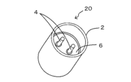
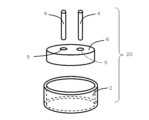
- FIG. 1 is a perspective view illustrating a bonded body according to an embodiment of the present disclosure.
- FIG. 2 is a cross-sectional view of the bonded body shown in FIG.
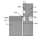
- FIG. 3 is an enlarged cross-sectional view of part A in FIG. 2 .
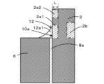
- 3 is an enlarged cross-sectional view showing another example of the joint in part A of FIG. 2.
- 3 is an enlarged cross-sectional view showing still another example of the joint portion in the portion A in FIG. 2.
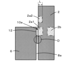
- FIG. 11 is an enlarged cross-sectional view showing an example in which a joint is not formed.
- FIG. 11 is an enlarged cross-sectional view showing another example in which a joint is not formed.
- FIG. 3 is an enlarged cross-sectional view of part B in FIG. 2 .
- 3 is an enlarged cross-sectional view showing another example of the joint in part B of FIG. 2.
- 3 is an enlarged cross-sectional view showing still another example of the joint portion in the portion B of FIG. 2.
- FIG. 4 is a cross-sectional view of another hermetic terminal of the present disclosure.
- 3 is an enlarged cross-sectional view showing another example of the joint in part A of FIG. 2.
- 3 is an enlarged cross-sectional view showing another example of the joint in part B of FIG. 2.
- 1 is a microscope image for explaining a method for identifying a joint in the present disclosure.
- 1 is a microscopic image for identifying the location of a surface layer remote from a joint in accordance with the present disclosure.
- FIG. 1 is a flow chart illustrating one embodiment of a method for manufacturing a conjugate of the present disclosure.
- FIG. 2 is an exploded view showing a method of assembling each member constituting the joined structure of the present disclosure.
- 1 is a microscope image (magnification: 1500x) of the crystal shape at the joint of the first metal member in the present disclosure.
- 1 is a microscope image (magnification: 1500x) of the crystal shape at a position away from the joint of the first metal member in the present disclosure.
- FIG. 14B is a microscopic image tracing the crystal shape shown in FIG. 14A.
- FIG. 14C is a microscopic image tracing the crystal shape shown in FIG. 14B.
- FIG. 15B shows a trace of the crystal shape shown in FIG. 15A.
- FIG. 15C shows a trace of the crystal shape shown in FIG. 15B.
- FIG. 16 is a graph showing the change in average crystal grain size versus distance ( ⁇ m) from the surface of the first metal member.
- 15B and FIG. 16 is a graph showing the crystal refinement rate (with the internal average crystal grain size taken as 100%) versus the depth ratio (%) from the surface of the first metal member.
- 1 is a microscope image (magnification: 1500x) of the crystal shape on the surface and inside of the joint of the second metal member in the present disclosure, in which the crystal shape is traced.
- 1 is a microscope image (magnification: 1500x) of the crystal shape of the surface and interior of the second metal member away from the joint in the present disclosure, and tracing of the crystal shape.
- FIG. 18B shows a trace of the crystal shape shown in FIG. 18A.
- FIG. 18C shows a trace of the crystal shape shown in FIG. 18B.
- 19C is a graph showing the change in average crystal grain size versus distance ( ⁇ m) from the surface of the second metal member, obtained from FIGS. 19A and 19B. 19B
- FIG. 19C is a graph showing the crystal refinement rate (with the internal average crystal grain size being 100%) versus the depth ratio (%) from the surface of the second metal member.
- FIG. 21B shows a trace of the crystal shape shown in FIG. 21A.
- FIG. 21C shows a trace of the crystal shape shown in FIG. 21B.
- FIG. 21C is a graph showing the change in average crystal grain size versus distance ( ⁇ m) from the surface of the metal element, determined from FIGS. 21A and 21B. 21B .
- FIG. 21C is a graph showing the crystal refinement rate (with the internal average crystal grain size taken as 100%) versus the depth ratio (%) from the surface of the metal element, obtained from FIGS. 21A and 21B .
- each of the drawings referred to below shows a simplified embodiment of the present disclosure. Therefore, the joint disclosed below may include any component not shown in each of the drawings referred to. Furthermore, the dimensions of the components in each drawing do not faithfully represent the dimensions of the actual components or the dimensional ratios of each component.
- the feed-through terminal described in Patent Document 1 mentioned above has low mechanical strength, so when stress is applied from the outside, cracks are likely to occur in the tubular member, tube, and pin made of metal material near the brazed joint.
- a large stress is applied to the metal material near the brazed joint, making it easy for cracks to occur in the tubular member, tube, and pin.
- the airtightness of the feed-through terminal decreases. In particular, cracks are likely to occur when repeated stress is applied.
- FIG. 1 is a perspective view showing a joint 20 according to this embodiment
- FIG. 2 is a cross-sectional view thereof.
- the joint 20 shown in FIGS. 1 and 2 can be used, for example, as an airtight terminal.
- the joint 20 has metal members including a first metal member 2 that is a cylindrical body and a second metal member 4 that is a columnar body, and is joined to an insulating member 6 that is an insulator.
- the insulating member 6 is located within the inner wall of the cylindrical body of the first metal member 2 and has a through hole 5.
- the second metal member is located through the through hole 5.
- the first metal member 2 and the second metal member 4 are joined to the insulating member 6 by a joining material 12.
- the insulating member 6 and the first metal member 2 and the second metal member 4 face each other via gaps 8a and 8b, respectively, and at least a portion of the joining material 12 is located within the gaps 8a and 8b.
- the first metal member 2 and the second metal member 4 may be in contact with the insulating member 6 without at least partially providing the gaps 8a and 8b.
- the joining material 12 include metals such as brazing filler metal, glass, etc.
- Figure 3 is an enlarged cross-sectional view of part A in Figure 2.
- the bonding material 12 that bonds the first metal member 2 including a cylindrical body and the insulating member 6 has a first extending portion 12a1 and a first filling portion 12a2 located in the gap 8a.
- the first extending portion 12a1 extends in a direction away from the insulating member 6 and has a fillet shape that contacts part of the surface of the first metal member 2 and part of the surface of the insulating member 6.
- a portion of the surface of the first metal member 2 that is in contact with the joining material 12 is defined as a first joining portion 10a.
- the surface of the first metal member 2 at a portion that is in contact with the first extending portion 12a1 and the first filling portion 12a2 is defined as a first joining portion 10a.
- the portion A in Fig. 2 has a form as shown in Fig. 4A and Fig. 4B as well as Fig. 3.
- the bonding material 12 has only the first filling portion 12a2.
- the bonding material 12 has only the first extending portion 12a1.
- the first filling portion 12a2 requires that the bonding material 12 is in contact with both the first metal member 2 and the insulating member 6 in the gap 8a. In contact with both, the bonding material 12 is present on the line segment that connects the first metal member 2 and the insulating member 6 at the shortest distance in the gap 8a. However, it is assumed that there is no void (closed gap in the bonding material 12) that is not in contact with the first metal member 2 or the insulating member 6 on the line segment. As shown in Figures 5A and 5B, when the bonding material 12 is not in contact with at least one of the first metal member 2 and the insulating member 6 (part D), it is not the first bonding portion 10a.
- the bonding material 12 is in contact with both the first metal member 2 and the insulating member 6, the part where the bonding material 12 is not present on the line segment that connects the first metal member 2 and the insulating member 6 at the shortest distance in the gap 8a, except for the void, is not the first bonding portion 10a.
- the average crystal grain size of the first surface layer 2a1 of the first metal member 2 at the first joint portion 10a is smaller than the average crystal grain size of the first interior 2b of the first metal member 2.
- the average crystal grain size of the first interior 2b of the first metal member 2 is Di ( ⁇ m) and the average crystal grain size of the first surface layer 2a1 is Ds ( ⁇ m)
- Ds ⁇ 0.7Di the average crystal grain size of the first surface layer 2a1 is 70% or less of the average crystal grain size Di of the first interior 2b.
- the formula: Ds ⁇ 0.6Di may be satisfied.
- the mechanical strength is improved because the crystals are finer in the first surface layer 2a1 of the first metal member 2. Therefore, for example, when stress (mechanical stress, thermal stress, etc.) is applied to the first metal member 2 from the insulating member 6 via the first joint portion 10a, it is possible to reduce the occurrence of cracks in the first surface layer 2a1 of the inner wall of the cylindrical body which is the first metal member 2. Since the average crystal grain size of the first interior 2b of the first metal member 2 is relatively large, even if fine cracks occur in the first surface layer 2a1 of the first metal member 2, the progression of the cracks into the interior can be reduced. Furthermore, since the first metal member 2 has high rigidity, even if stress is repeatedly applied to the joint 20, breakage is less likely to occur.
- the first surface layer 2a1 of the first metal member 2 refers to the region from the surface (inner wall surface) of the first metal member 2 to a depth L of 5% of the thickness. For example, if the thickness of the first metal member 2, which is a cylindrical body, is 0.75 mm, the first surface layer 2a1 refers to the region from the surface to a depth L of 0.0375 mm in the thickness direction.
- the first interior 2b of the first metal member 2 refers to a region having a depth of 20% to 80% of the thickness from the surface (inner wall surface) of the first metal member 2. For example, if the thickness of the first metal member 2 is 0.75 mm, the first interior 2b is a region having a depth of 0.15 mm to 0.6 mm from the surface in the thickness direction.
- the average crystal grain size of the surface layer 2a2 away from the first joint 10a of the first metal member 2 is smaller than the average crystal grain size of the first interior 2b of the first metal member 2, and larger than the average crystal grain size of the first surface layer 2a1 of the first metal member 2 in contact with the first joint 10a.
- Figure 6 is an enlarged cross-sectional view of part B in Figure 2.
- the bonding material 12 that bonds the second metal member 4 including the columnar body to the insulating member 6 has a second extension portion 12b1 having a fillet shape that contacts a part of the surface of the second metal member 4 that extends in a direction away from the insulating member 6 and a part of the surface of the insulating member 6, and a second filling portion 12b2 located in the gap portion 8b.
- the portion of the surface of the second metal member 4 that contacts the joining material 12 is the second joining portion 10b.
- the portion of the surface of the second metal member 4 that contacts the second extension portion 12b1 and the second filling portion 12b2 is the second joining portion 10b.
- the bonding material 12 has only the second filling portion 12b2.
- the bonding material 12 has only the second extending portion 12b1.
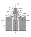
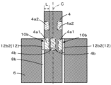
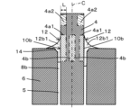
- the second bonding portion 10b in contact with the bonding material 12 includes not only the form shown in FIG. 6 but also the forms shown in FIGS. 7A and 7B.
- the average crystal grain size of the second surface layer 4a1 of the second metal member 4 at the second joint portion 10b is smaller than the average crystal grain size of the second interior 4b of the second metal member 4.
- the average crystal grain size of the second interior 4b of the second metal member 4 is Di ( ⁇ m) and the average crystal grain size of the second surface layer 4a1 is Ds ( ⁇ m)
- this can be expressed by the formula: Ds ⁇ 0.7Di.
- Ds ⁇ 0.6Di may also be true.
- the second surface layer 4a1 of the second metal member 4 refers to the region from the surface of the second metal member 4 to a depth L of 5% of the thickness (half the diameter in the case of a columnar body such as a solid pin). For example, if the second metal member 4 has a diameter of 1.6 mm (radius of 0.8 mm), the second surface layer 4a1 is the region from the surface to a depth L of 0.04 mm in the radial direction.
- the second interior 4b of the second metal member 4 refers to a region that is 20% or more deep relative to the radial thickness from the surface of the second metal member 4 (half the diameter in the case of a columnar body such as a solid pin). For example, if the diameter of the second metal member 4 is 1.6 mm (radius 0.8 mm), the second interior 4b is a region that is deeper than 0.16 mm in the radial direction from the surface. The upper limit of the second interior 4b is the center C (axis) of the second metal member 4.
- the average crystal grain size of the surface layer 4a2 away from the second joint 10b is smaller than the average crystal grain size of the second interior 4b of the second metal member 4, and is larger than the average crystal grain size of the second surface layer 4a1 of the second metal member 4 that contacts the second joint 10b.
- the joint 20 shown in FIG. 2 is joined to the first metal member 2 and the second metal member 4 on one side (upper side) of the insulating member 6, but it may be joined to the first metal member 2 and the second metal member 4 on both sides (upper and lower sides) of the insulating member 6, as in the joint 21 shown in FIG. 8.
- the insulating member 6 may have chamfered portions 14 on the outer peripheral surface facing the first metal member 2 and on the inner wall surface of the through hole 5 through which the second metal member 4 is inserted.
- the chamfered portion 14 may include at least one of a C surface and an R surface.
- the chamfered portion 14 is located on one side (upper side) of the insulating member 6, but it may be located on both sides (upper and lower) of the insulating member 6.
- FIG. 10 is a microscope image showing a cross section of the second joint 10b and its surrounding area in this disclosure.
- the second extension portion 12b1 (second joint 10b) is used as an example for explanation, but the first extension portion 12a1 (first joint 10a) is also identified using the same identification method.
- a first straight line L1 is drawn on the surface of the insulating member 6 and its extension line.
- the first straight line L1 intersects with the second metal member 4.
- a second straight line L2 is drawn on the contour of the outer circumferential surface of the second metal member 4.
- the second straight line L2 intersects with the first straight line L1.
- the intersection of the first straight line L1 and the second straight line L2 is defined as an origin P1.
- a third straight line L3 is drawn starting from the origin P1 and making an angle of 1° from the second straight line L2 toward the second extending portion 12b1.
- the point where the third straight line L3 and the contour of the second extending portion 12b1 first intersect is defined as point P2.
- the second extending portion 12b1 is defined as the bonding material 12 located between the first straight line L1 and the fourth straight line L4.
- the second bonding portion 10b in the second extending portion 12b1 is the surface of the second metal member 4 located between the first straight line L1 and the fourth straight line L4.
- the second bonding portion 10b is illustrated as being located between the first straight line L1 and the fifth straight line L5.
- the second extending portions 12b1 are provided on both sides of the second metal member 4, it is preferable to identify the second joint portions 10b for each of the second extending portions 12b1.
- the angle between the second straight line L2 and the third straight line L3 is set to 1°, but may be appropriately selected within the range of 0.8° to 1.6°. If it is within the above range, the crystals in the second surface layer 4a1 of the second bonding portion 10b are finer.
- the second extension portion 12b1 extends thinly in a direction away from the insulating member 6 through the point P2, but since it is a thin film, it is considered that it does not substantially contribute to the bonding.
- Figure 10 is a schematic diagram for easy understanding of the method of identifying the second bonding portion 10b, and in reality, the point P2 is located near the point P4. In addition, if the second extending portion 12b1 (particularly the end portion thereof) has an irregular convex portion or bulge portion, the convex portion or bulge portion should not be taken into consideration when specifying the second extending portion 12b1.
- the portion of the extension that is 15 ⁇ m or more in thickness may be designated as the second extension 12b1.
- the portion of the extension above the fifth line L5 that is parallel to the first line L1 has a thickness of less than 15 ⁇ m, and is considered not to substantially contribute to the joint.
- the second joint 10b may be identified by using the arc-shaped cross-sectional shape of the second extension 12b1.
- the arc C1 is drawn so as to follow the contour of the second extension 12b1 as closely as possible. Following as closely as possible means that the difference between the arc C1 and the contour of the second extension 12b1 is minimized.
- the difference between the contour of the arc C1 and the contour of the second extension 12b1 can be obtained, for example, as follows.
- a straight line is drawn from the center of the arc C1 toward the arc C1, and an intersection point E between the straight line and the arc C1 and an intersection point F between the straight line and the contour of the second extension 12b1 are identified.
- the direction from the center of the arc C1 toward the arc C1 is defined as the positive direction
- the length of the straight line from the intersection point E to the intersection point F is defined as the difference between the contour of the arc C1 and the contour of the second extension 21b.
- nine straight lines are drawn from the center of the arc C1, dividing the arc C1 into nine equal parts, and the difference between the contours of the arc C1 and the second extension portion 12b1 is calculated for each straight line.
- the state in which the sum of these differences is the smallest is considered to be the smallest difference between the arc C1 and the second extension portion 12b1.
- the number of equal parts into which the arc C1 is divided may be appropriately adjusted according to the shape of the second extension portion 21b.
- the perimeter of the arc C1 is 1/4 of the circumference.
- the arc C1 has points P3 and P4 at both ends.
- Point P4 of the arc C1 is the point closest to the second metal member 4.
- a sixth straight line L6 is drawn that passes through point P4 of the arc C1 and is parallel to the first straight line L1 (in FIG. 10, it overlaps with the fifth straight line L5).
- the second joint portion 10b is a portion between the first straight line L1 and the sixth straight line L6.
- the first extending portion 12a1 is also identified by the same identification method.
- the upper end of the second joint portion 10b is defined as the starting end (0 mm).
- the average crystal grain size of the surface layer and the second interior 4b of the second metal member 4 is measured at the starting end and at multiple portions along the surface of the second metal member 4 away from the starting end (for example, multiple portions spaced 0.25 mm apart as shown in FIG. 11 ).
- Refinement rate (%) ⁇ (average crystal grain size of surface layer)/(average crystal grain size of interior layer) ⁇ x 100
- the calculation results are shown in Table 1.
- the surface layer and the inside are as described above.
- the measurement interval is not limited to 0.25 mm and can be changed as appropriate.
- the area away from the starting point (0 mm), where the refinement rate (%) is greater than that of the starting point and where the refinement rate (%) exceeds 80% is defined as the surface layer 4a2 away from the second joint 10b.
- the surface layer 2a2 away from the first joint 10a can be identified using the same method as the surface layer 4a2 away from the second joint 10b.
- FIG. 12 is a flow chart showing the manufacturing method
- Figure 13 is an exploded view showing the assembly method of each member.
- an insulating member 6 which is an insulator serving as a raw material, metal members (a first metal member 2 and a second metal member 4), and a joint material 12 containing metal or glass are prepared (preparation process).
- the insulator refers to an insulating material having a volume resistivity at 20° C. of 10 10 ⁇ m or more.
- the insulating member 6 is preferably made mainly of any one of alumina, zirconia, silicon nitride, silicon carbide, forsterite, cordierite, and sapphire. Of these insulating members 6, ceramic materials are inexpensive and have excellent mechanical strength, while sapphire has excellent light transmittance.
- the main component of the insulating member refers to a component that occupies 60% by mass or more of the total 100% by mass of the components that constitute the insulating member. In particular, the main component is preferably a component that occupies 95% by mass or more of the total 100% by mass of the components that constitute the insulating member.
- the components that constitute the insulating member may be determined using an X-ray diffraction device (XRD). The content of each component may be determined by identifying the component, and then using an X-ray fluorescence analyzer (XRF) or an ICP emission spectrometer to determine the content of the elements that constitute the component, and converting it into the identified component.
- XRD X
- the first metal member 2 and the second metal member 4 contain Fe, Ni, and Co in order to reduce the thermal expansion coefficient and reduce the residual stress generated by bonding with the insulating member 6, and the total content of Fe, Ni, and Co is preferably 99 mass% or more. This can reduce cracks in the first metal member 2 and the second metal member 4.
- the insulating member 6 may be mainly composed of alumina, whose thermal expansion coefficient is similar to that of the first metal member 2 and the second metal member 4.
- the first metal member 2 and the second metal member 4 may preferably contain Fe in an amount of 40 mass% or more and 56 mass% or less, Ni in an amount of 25 mass% or more and 40 mass% or less, and Co in an amount of 10 mass% or more and 30 mass% or less.
- the first metal member 2 may be an Fe-Ni alloy such as Invar 36 (Fe 54% by mass, Ni 36% by mass) or an Fe-Ni-Co alloy such as Kovar (Fe 53% by mass, Ni 29% by mass, Co 17% by mass).
- the columnar second metal member 4 may be a metal having the same composition as the first metal member 2.
- the second metal member 4 may be a metal different from that of the first metal member 2, such as Cu (copper) or an alloy containing Cu as a main component.
- the first metal member 2 may be made of Cu or an alloy whose main component is Cu, and the second metal member 4 may be made of an alloy such as Kovar or Invar 36.
- the joining material 12 may include a metal, such as a brazing material, or a glass.
- At least one of the first metal member 2 and the second metal member 4 preferably contains a composition of 40% by mass or more and 56% by mass or less of Fe, 25% by mass or more and 40% by mass or less of Ni, and 10% by mass or more and 30% by mass or less of Co, the insulating member 6 contains alumina, and the joining material 12 contains Ag and Cu, and is a brazing material in which the total content of Ag and Cu is 90% by mass or more.
- the columnar second metal member 4 is inserted into the through hole 5 of the insulating member 6, and the insulating member 6 is inserted into the cylindrical first metal member 2.
- a bonding material 12 is placed on either the opposing surface between the insulating member 6 and at least the first metal member 2 or at least one surface of the insulating member 6 near the opposing surface, and on either the opposing surface between the insulating member 6 and at least the second metal member 4 or at least one surface of the insulating member 6 near the opposing surface, to obtain an assembly (assembly process).
- the assembly is heated in a vacuum or in an inert gas to melt the bonding material 12, and then cooled to below 200°C to solidify the bonding material 12. This results in a pre-bonded body in which the insulating member 6 and the first metal member 2, and the insulating member 6 and the second metal member 4 are bonded together (bonding process).
- a metallized layer may be formed on the insulating member 6 in advance.
- An example of the metallized layer is a Mo-Mn-based metallized layer.
- a plating layer may be formed on the metallized layer.
- the plating layer includes Ni plating. Regardless of whether the metallized layer is formed or not, a plating layer may be formed on at least one of the inner wall surface of the first metal member 2 and at least the outer circumferential surface of the second metal member 4.
- the plating layer includes Ni plating.
- the obtained pre-joint is cooled at an ambient temperature of -100°C or lower to obtain the joint 20 (cooling process).
- the crystals in the portions of the first metal member 2 and the second metal member 4 that abut the joint i.e., the portions of the first surface layer 2a1 and the second surface layer 4a1
- the mechanical strength of the refined portions is improved, the occurrence of cracks in the first joint 10a and the second joint 10b is reduced, and the mechanical strength of the joint 20 between the metal and the ceramic, which is an insulator, is improved, and breakage can be reduced.
- the cooling can be performed, for example, by immersing in a cooling liquid of ⁇ 100° C. or less.
- the cooling liquid include liquid oxygen (boiling point ⁇ 183° C.), liquid nitrogen (boiling point ⁇ 196° C.), liquid hydrogen (boiling point ⁇ 253° C.), and liquid helium (boiling point ⁇ 269° C.).
- the immersion time is 1 minute or more, and may be 10 minutes or more.
- the pre-joined body may be cooled to ⁇ 100° C. or less in a gas atmosphere having an atmospheric temperature of ⁇ 100° C. or less, instead of in a liquid.
- the average crystal grain size of the first surface layer 2a1 and the second surface layer 4a1 can be reduced.
- the immersion time may be appropriately adjusted so as to obtain a desired average crystal grain size.
- the metal crystals of the first surface layer 2a1 and the second surface layer 4a1 of the first joint portion 10a and the second joint portion 10b are finer than those of the other portions, rather than being entirely made of metal, because residual stress is generated in the first surface layer 2a1 and the second surface layer 4a1 of the first joint portion 10a and the second joint portion 10b due to the joining.
- the bonded body of the present disclosure can be used as an electromagnetic wave transmitting window member for introducing electromagnetic waves into a semiconductor manufacturing device, outputting high frequency waves from an accelerator, etc.
- This window member has a cylindrical first metal member 2, and has a structure in which the outer peripheral surface of an insulating member 6 is bonded to the inner wall surface of the first metal member 2.
- the second metal member 4 including the columnar body described above is not necessarily required.
- the insulating member 6 used should preferably contain any one of alumina, zirconia, silicon nitride, silicon carbide, forsterite, cordierite, and sapphire as its main component.
- the electromagnetic wave transmitting window member can also be used as an observation window, for example, for visually checking the inside of a container, a pipe, a semiconductor manufacturing device, a furnace, or other equipment.
- the joint of the present disclosure can also be used as a power supply terminal.
- the power supply terminal is used, for example, as a power supply terminal for introducing a large current of 100 A or more into equipment.
- This power supply terminal has a second metal member 4 including a columnar body, and the insulating member 6 has a through hole 5 through which the second metal member 4 passes.
- the cylindrical first metal member 2 described above is not necessarily required.
- the assembly of the present disclosure can also be used as an airtight terminal that requires high airtightness in the above-mentioned power supply terminal.
- the airtight terminal is used, for example, as a power supply terminal that introduces current from the outside into a vacuum container, a signal terminal that transmits a signal from a sensor provided inside a container, piping, equipment, etc. that requires airtightness to the outside, etc.
- this airtight terminal has an insulating member 6 located inside the inner wall of the cylindrical body of the first metal member 2 and has a through hole 5 through which a columnar second metal member 4 passes.
- the first metal member 2 and the second metal member 4 preferably contain a composition of 40% by mass or more and 56% by mass or less of Fe, 25% by mass or more and 40% by mass or less of Ni, and 10% by mass or more and 30% by mass or less of Co, the insulating member 6 contains alumina, and the joint material 12 contains Ag and Cu, and is a brazing material having a total content of Ag and Cu of 90% by mass or more. This provides excellent airtightness between the cylindrical body, which is the first metal member 2, and the insulating member 6, and between the columnar body, which is the second metal member 4, and the insulating member 6, as well as excellent bonding strength therebetween.
- the hermetic terminal has excellent airtightness even when used in an environment of -100°C or below, and can reduce cracks in the first metal member 2, the second metal member 4 and the insulating member 6 that constitute the hermetic terminal.
- Example 1 A bonded body 21 having the cross-sectional structure shown in Fig. 8 was produced, and the crystal size reduction in the first bonding portion 10a (see Fig. 9A) of the cylindrical first metal member 2 was investigated.
- the components constituting the bonded body 21 are as follows.
- First metal member 2 A cylindrical body (sleeve) having a thickness of 0.75 mm made of an Fe-Ni-Co alloy (Kovar containing 53% by mass of Fe, 29% by mass of Ni, and 17% by mass of Co).
- Second metal member 4 A columnar body (pin) having a diameter of 1.6 mm, made from the same Fe—Ni—Co alloy as the first metal member 2.
- Insulating member 6 A sintered body containing 99.5% by mass of alumina, and has two through holes 5 through which the second metal member 4 is inserted.
- Joining material 12 A brazing material containing Ag and Cu, the total content of Ag and Cu being 90 mass % or more. After assembly, the bonded body 21 was immersed in liquid nitrogen at -100° C. or lower for 10 minutes.
- the joint 21 thus treated at low temperature is embedded in resin and then cut with a diamond cutter.
- the cut surface is roughly polished with a diamond disk, buffed with diamond abrasive grains, and then buffed with silica abrasive grains. This results in a mirror-like surface.
- the polished surface is appropriately chemically polished with a 5% nitric acid-ethanol mixed solution or aqua regia (a liquid in which concentrated nitric acid and concentrated hydrochloric acid are mixed in a volume ratio of 3:1).
- physical polishing may be appropriately performed with focused ion beam (FIB) processing, iomilling processing, etc. This makes it easier to observe the crystal grain boundaries of the metal.
- FIB focused ion beam
- FIGS. 14A and 14B are microscopic images of the crystal shape of the cross section of the cylindrical body that is the first metal member 2, where Fig. 14A shows the crystal shape from the first surface layer 2a1 to the first interior 2b of the first metal member 2 at the first joint 10a, and Fig. 14B shows the crystal shape from the surface layer 2a2 to the interior of the first metal member 2 at a position (normal portion) away from the first joint 10a.
- the horizontal direction indicates the depth direction from the surface of the first metal member 2
- the vertical direction i.e., the direction along the surface of the first metal member 2 indicates the measurement direction of the average crystal grain size.
- Figures 15A and 15B are microscope images obtained by tracing the crystal shapes shown in Figures 14A and 14B, respectively. That is, Figures 15A and 15B were created by importing the electronic data of the microscope images shown in Figures 14A and 14B into PowerPoint (a trademark of Microsoft Corporation) and tracing the outline of the crystal using a drawing tool. The microscope images may also be created by printing out the microscope images, placing a piece of tissue paper on the surface, and tracing the outline of the crystal onto the tissue paper. 16A and 16B show traces of the crystal shapes shown in FIGS. 15A and 15B, respectively.
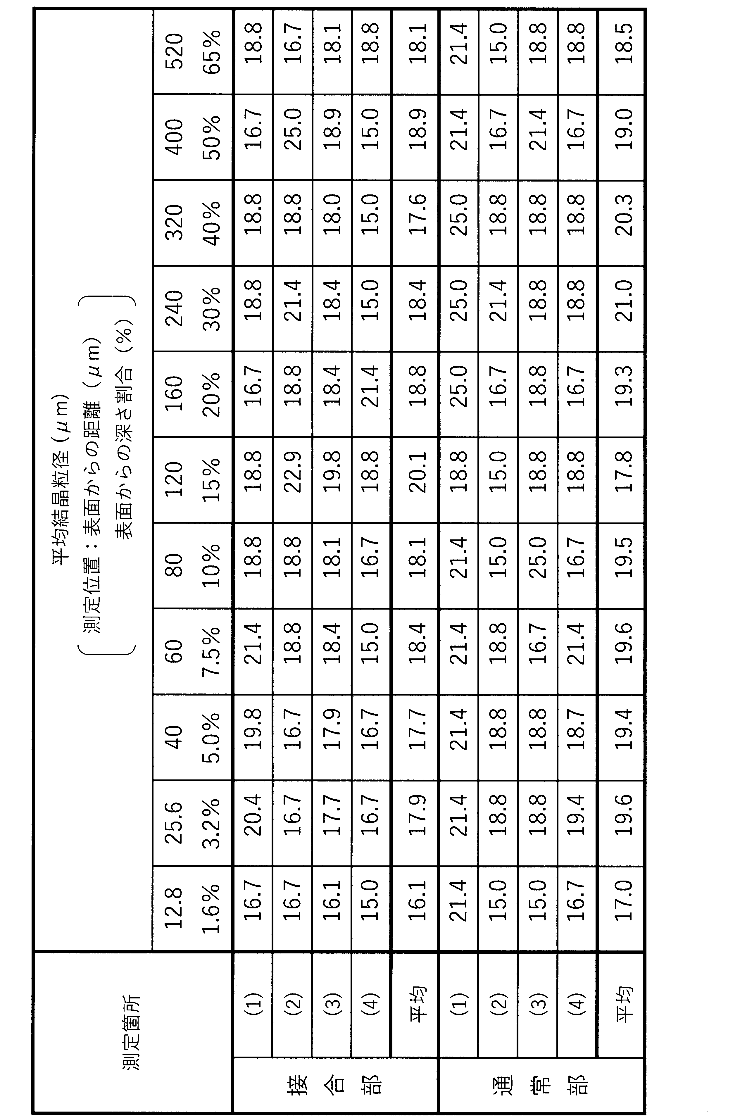
- the measurement positions of the average crystal grain size are indicated by the distance d ( ⁇ m) from the surface in the depth direction and the percentage (%).
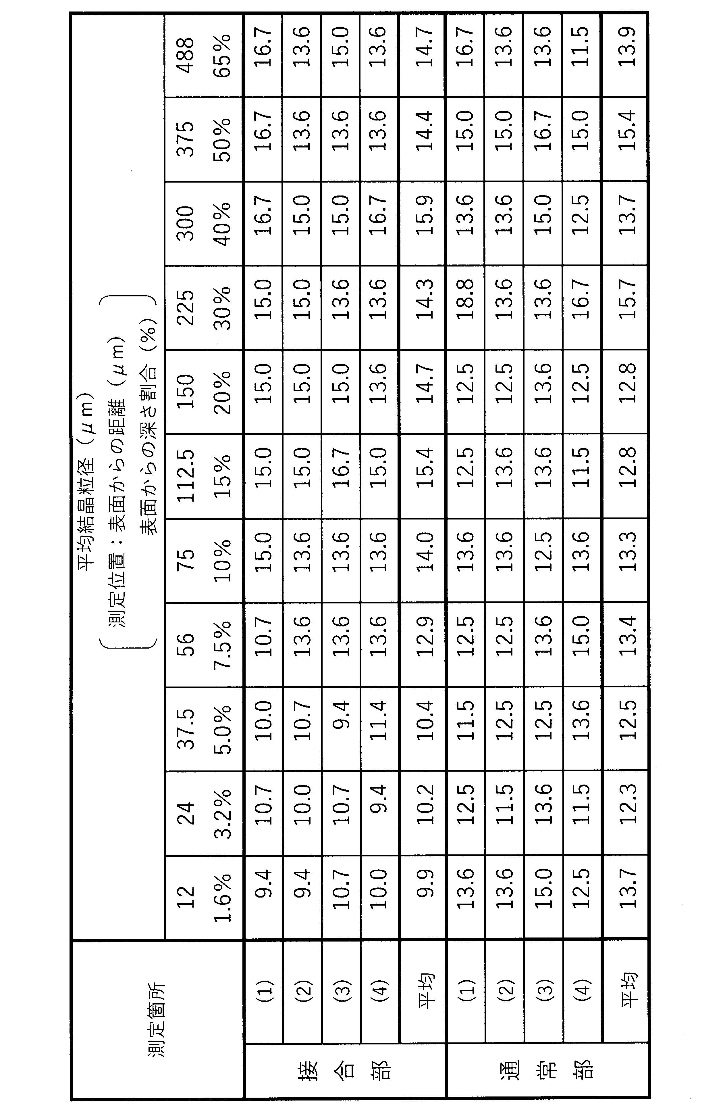
- the percentage (%) in the depth direction is calculated from the formula: (d/0.75) ⁇ 100, with the thickness of the first metal member 2 of 0.75 mm being 100%.
- the measurement positions indicated by the percentage (%) in the depth direction were arbitrarily set to 1.6%, 3.2%, 5.0%, 7.5%, 10%, 15%, 20%, 30%, 40%, 50%, and 65%.
- These measurement positions are indicated by vertical lines parallel to the measurement direction of the average crystal grain size on the traces in Figures 16A and 16B. At each measurement point on the trace in Figures 16A and 16B, a straight line of 150 ⁇ m is drawn along the measurement direction of the average crystal grain size.
- the number of crystal counts is calculated by subtracting 1 from the total number of points where this line intersects with the grain boundaries.
- the number obtained by dividing the length of the line (150 ⁇ m) by the number of crystal counts is calculated as the average crystal grain size.
- the measurement points of the average crystal grain size will be described.
- FIG. 8 shows four first extensions 12a1 that join the left and right first metal members 2 and the insulating member 6.
- the measurement points are four points of the first joint 10a in contact with each first extension 12a1 and four points in the normal portion away from each first joint 10a.
- the average crystal grain size was determined as the average value of the average crystal grain size at each measurement position.
- the results are shown in Table 2 and FIG. 17A.
- the graph in FIG. 17A shows the change in the average crystal grain size with respect to the distance ( ⁇ m) from the surface, that is, the distance ( ⁇ m) in the depth direction from the surface.
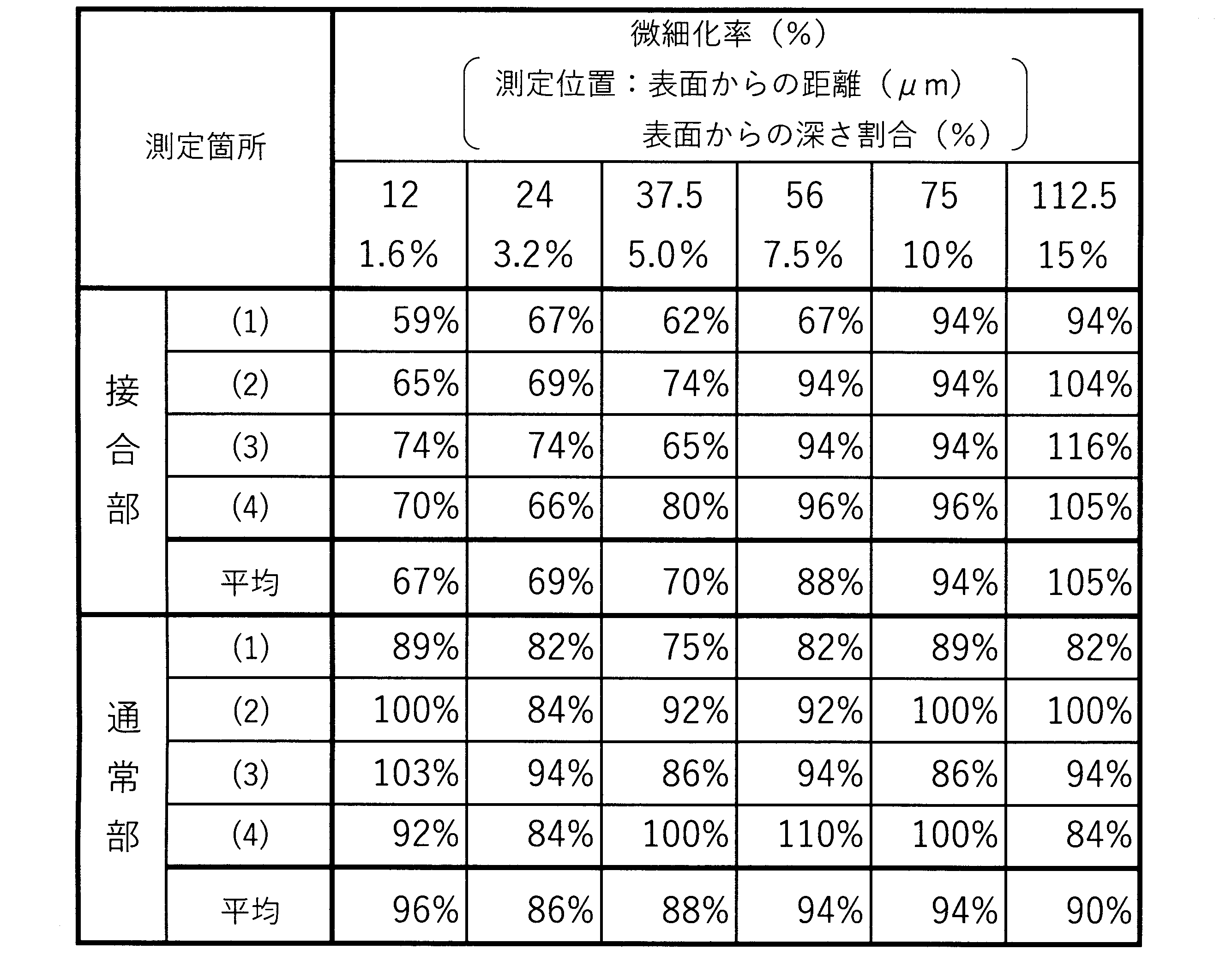
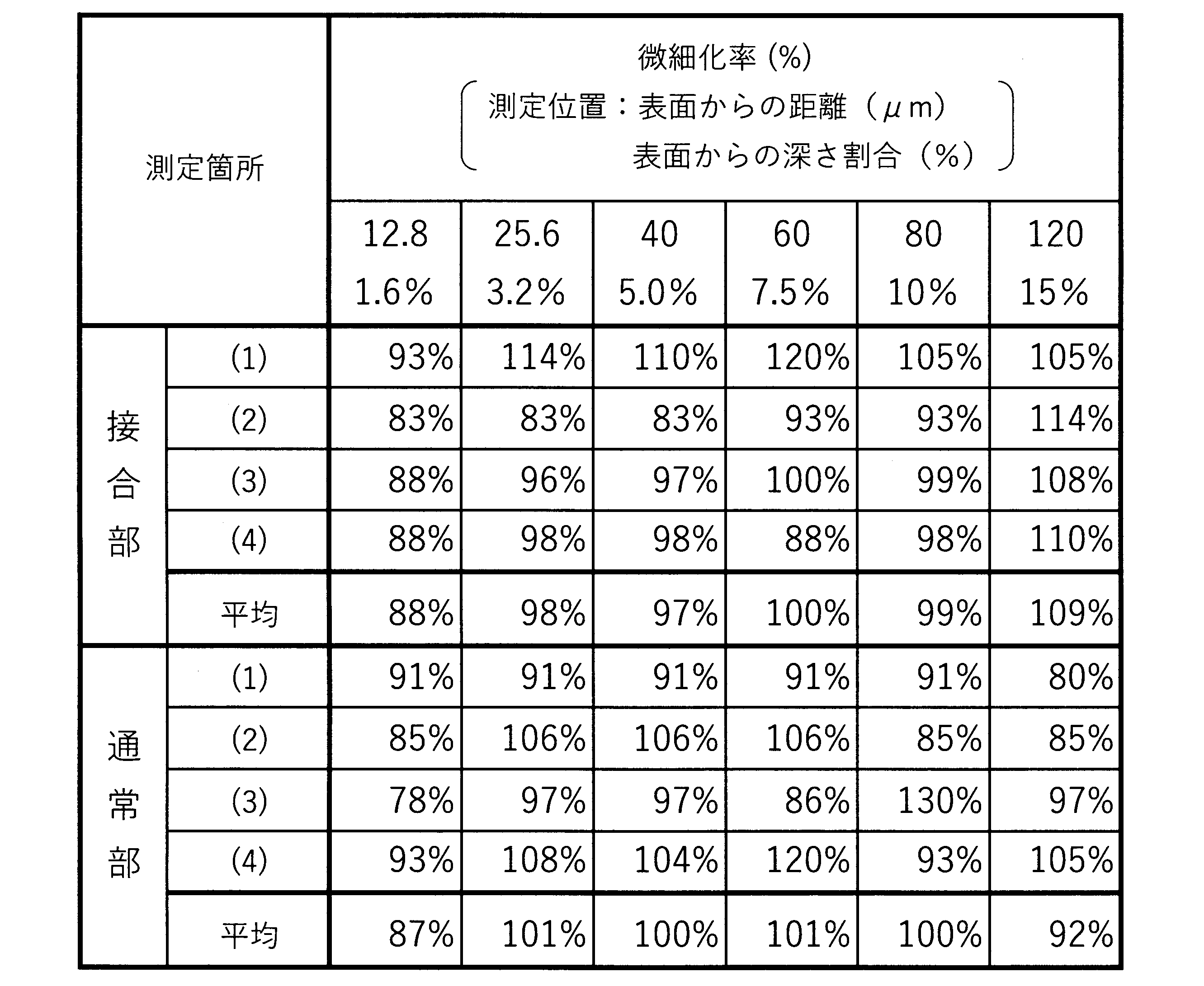
- Table 3 shows the crystal refinement rate calculated from the average crystal grain size at each measurement position from the surface of the first metal member 2 to a depth of 15% and the average crystal grain size inside (a region from the surface to 20% to 65% of the depth) based on the measurement results in Table 2.
- the crystal refinement rate is calculated using the following formula.
- Formula: refinement rate (%) ⁇ (average crystal grain size at each measurement position)/(internal average crystal grain size) ⁇ x 100
- the graph in FIG. 17B shows the change in the crystal refinement rate versus the depth percentage (%) from the surface.
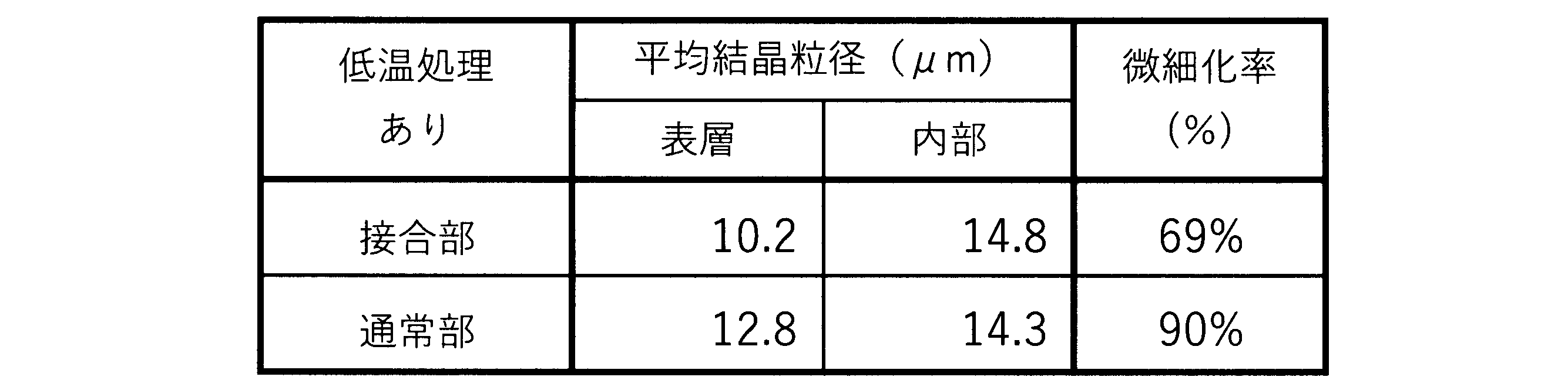
- Table 4 shows the crystal refinement rate calculated from the average crystal grain size in the surface layer (region up to 5% depth from the surface) and the average crystal grain size in the interior (region 20% to 65% depth from the surface) of the first metal member 2 based on the measurement results in Table 2.
- the crystal refinement rate is calculated by the following formula.
- Refinement rate (%) ⁇ (average crystal grain size of surface layer)/(average crystal grain size of interior layer) ⁇ x 100
- the first surface layer 2a1 of the first joint 10a has a smaller average crystal grain size than the first interior 2b.
- the surface layer of the normal portion also has a smaller average crystal grain size than the interior, but the average crystal grain size is larger than that of the first surface layer 2a1 of the first joint 10a.
- the normal portion has a crystal refinement rate of 90%, which means that the crystals are hardly refined at all, whereas the first surface layer 2a1 of the first joint 10a has a refinement rate of 69%.
- Example 2 Using the bonded body 21 used in Example 1, the crystal refinement in the second bonded portion 10b (see FIG. 9B) of the columnar second metal member 4 bonded to the insulating member 6 was examined.
- 18A and 18B are microscopic images of the crystal shape of the cross section of the columnar body (pin) of the second metal member 4, where FIG. 18A shows the crystal shape from the second surface layer 4a1 to the second interior 4b of the second metal member 4 at the second joint 10b, and FIG. 18B shows the crystal shape from the surface layer 4a2 to the interior of the second metal member 4 at a position (normal portion) away from the second joint 10b.
- the crystal shape is traced.
- FIG. 19A and 19B are diagrams showing the traces of the crystal shapes shown in FIGs. 18A and 18B, respectively.
- the measurement points of the average crystal grain size will be described.
- FIG. 8 shows eight second extensions 12b1 that join the left and right second metal members 4 and the insulating member 6.
- the measurement points are four points of the second joint 10b at the portion contacting each of the two second extensions 12b1 that join the left second metal member 4 and the upper surface of the insulating member 6, and the two second extensions 12b1 that join the right second metal member 4 and the lower surface of the insulating member 6, and four points in the normal portion away from each second joint 10b.
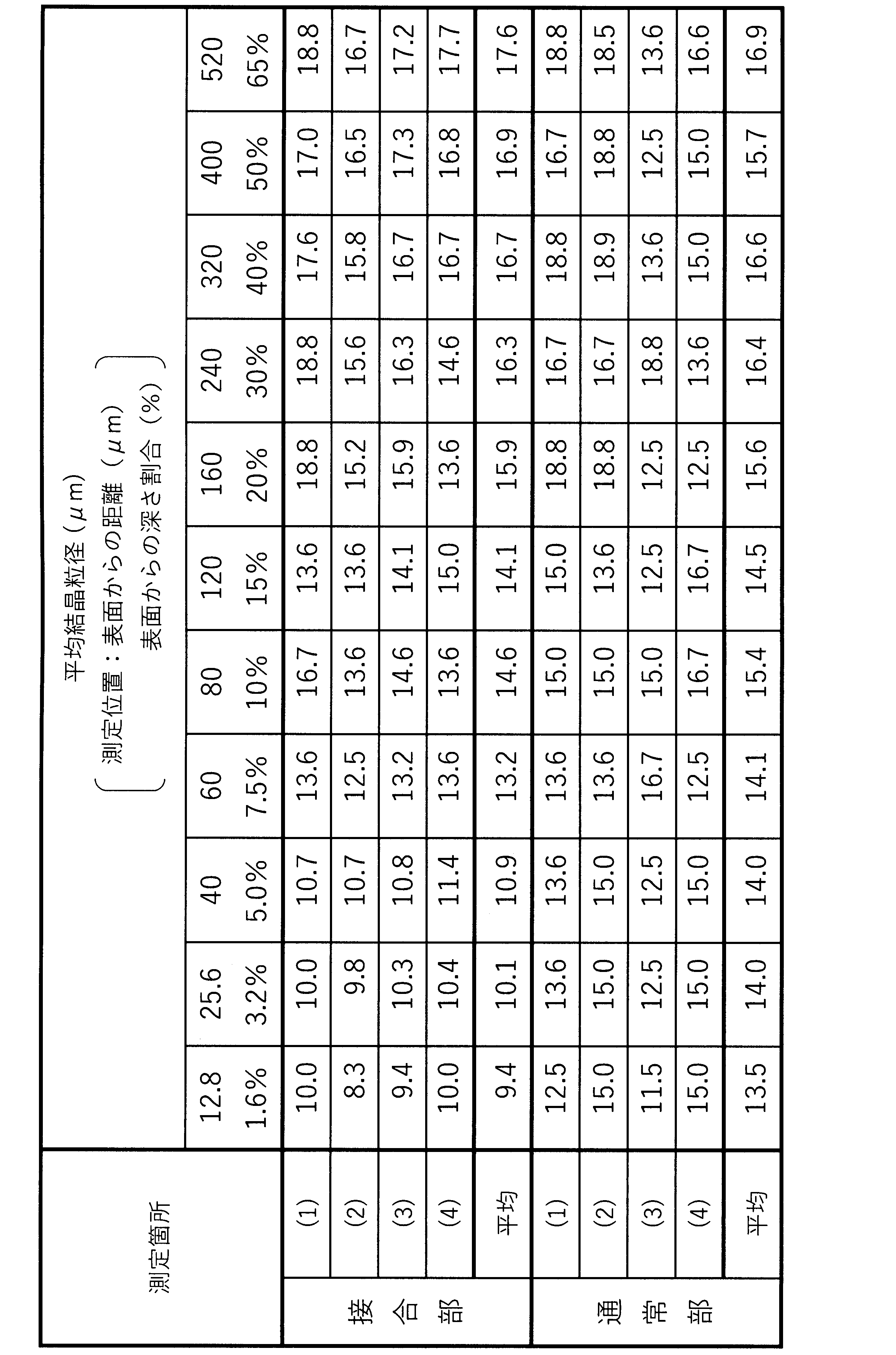
- the average crystal grain size was the average value of the average crystal grain size at each measurement position. The rest was tested in the same manner as in Example 1.
- the results are shown in Table 5.
- the average grain size of the second bonded portion 10b and the normal portion distant therefrom in the bonded body that was not subjected to the low-temperature treatment was also tested in the same manner.
- the results are shown in Table 6.
- the graph in FIG. 20A shows the results of Tables 5 and 6, and indicates the change in average crystal grain size versus the distance ( ⁇ m) from the surface.
- Tables 7 and 8 show the crystal refinement ratios calculated from the average crystal grain size at each measurement position from the surface of the second metal member 4 to a depth of 15% and the average crystal grain size inside (a region from the surface to 20% to 65% of the depth) based on the measurement results in Tables 5 and 6.
- the crystal refinement ratio is calculated using the following formula.
- Formula: refinement rate (%) ⁇ (average crystal grain size at each measurement position)/(internal average crystal grain size) ⁇ x 100
- the graph in FIG. 20B shows the results of Tables 7 and 8, and indicates the change in average crystal grain size versus the depth ratio (%) from the surface.
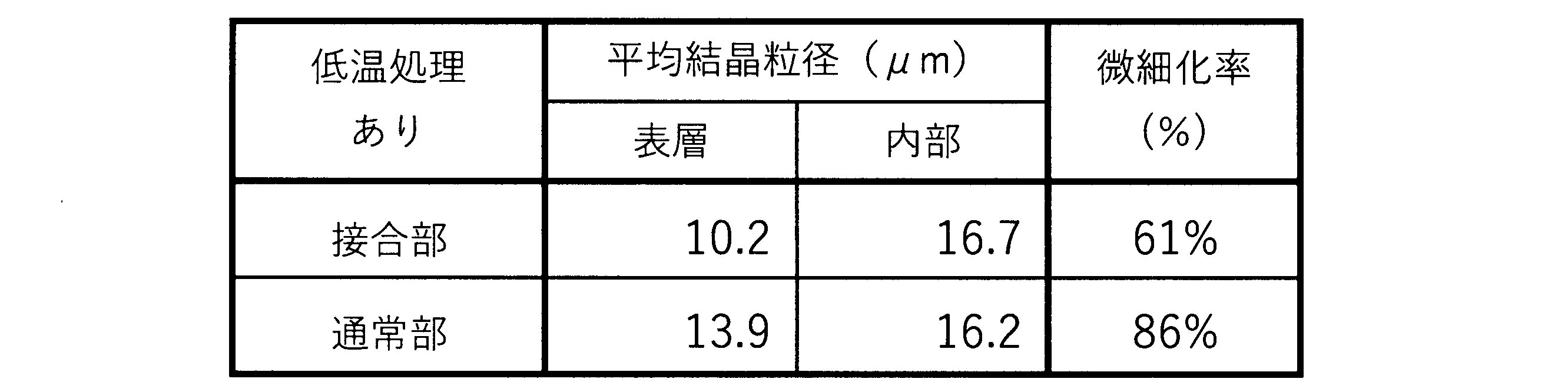
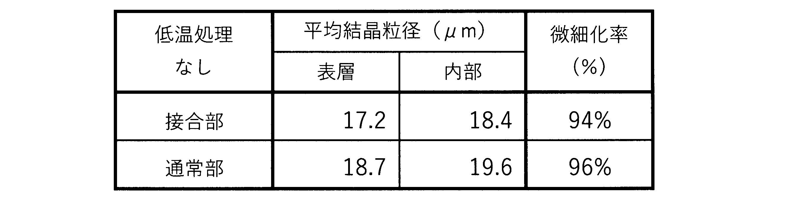
- Tables 9 and 10 show the crystal refinement ratios calculated from the average crystal grain size in the surface layer (region up to 5% depth from the surface) and the average crystal grain size in the interior (region 20% to 65% depth from the surface) of the second metal member 4 based on the measurement results in Tables 7 and 8.
- the crystal refinement ratio is calculated using the following formula.
- Refinement rate (%) ⁇ (average crystal grain size of surface layer)/(average crystal grain size of interior layer) ⁇ x 100
- the crystals were refined in the second surface layer 4a1 of the second bonded portion 10b (crystal refinement rate: 61%), and when the average crystal grain size of the second interior 4b was taken as 100%, the refinement rate of the second surface layer 4a1 was 56 to 67%.
- the refinement rate was 86%, and almost no refinement of the crystals was observed.
- the refinement rate in the joined portion was 94%, while the refinement rate in the normal portion was about 96%, meaning that the crystals in the surface layer portion were not substantially refined.
- Figures 22A and 22B are diagrams showing the traces of the crystal shapes shown in Figures 21A and 21B, respectively.
- the measurement of the average crystal grain size and the calculation of the refinement rate were performed in the same manner as in Example 1.
- the results are shown in Tables 11, 12, and 13 and in Figures 23A and 23B.
- no refinement of the crystals was observed in either the metal element that had been subjected to low-temperature treatment or the metal element that had not been subjected to low-temperature treatment.
Landscapes
- Chemical & Material Sciences (AREA)
- Engineering & Computer Science (AREA)
- Ceramic Engineering (AREA)
- Materials Engineering (AREA)
- Structural Engineering (AREA)
- Organic Chemistry (AREA)
- Ceramic Products (AREA)
Abstract
Description
図2におけるA部分は、図3だけでなく、図4A、4Bに示すような形態を有する。図4Aでは、接合材12は第1充填部12a2のみを有する。図4Bでは、接合材12は第1延出部12a1のみを有する。
第1充填部12a2は、間隙部8a内で、接合材12が第1金属部材2と絶縁部材6の両方に接していることが必要である。両方に接しているとは、間隙部8a内で第1金属部材2と絶縁部材6とを最短距離で結ぶ線分上に接合材12が存在していることである。ただし、線分上の第1金属部材2または絶縁部材6に接しないボイド(接合材12中の閉じた空隙)はないものとして扱う。図5A、5Bに示すように、接合材12が第1金属部材2と絶縁部材6の少なくとも一方に接していない場合(D部分)は、第1接合部10aではない。接合材12が第1金属部材2と絶縁部材6のいずれにも接している場合でも、ボイドを除いて、間隙部8a内で第1金属部材2と絶縁部材6とを最短距離で結ぶ線分上に接合材12が存在していない部分は、第1接合部10aではない。
例えば、第1金属部材2の第1内部2bの平均結晶粒径をDi(μm)、第1表層2a1の平均結晶粒径をDs(μm)とするとき、式:Ds≦0.7Diで表すことができる。すなわち、第1表層2a1の平均結晶粒径Dsが第1内部2bの平均結晶粒径Diの70%以下であることをいう。式:Ds≦0.6Diの関係を有してもよい。
第1金属部材2の第1内部2bの平均結晶粒径は比較的大きいので、第1金属部材2の第1表層2a1に微細なクラックが発生したとしても、クラックの内部への進展を低減することができるとともに、第1金属部材2の剛性が高いので接合体20に応力が繰り返しかかった場合でも、破壊が起こりにくくなる。
これにより、第1内部2bへのクラックの進展を低減しつつ、第1接合部10aから離れた表層2a2へのクラックの進展をも低減することができる。繰り返し応力がかかった場合にも筒状体である第1金属部材2の破壊が低減できる。
第1接合部10aから離れた表層2a2の特定方法は後述する。
接合材12と接する第2接合部10bは、図6に示した形態のみならず、図7Aおよび図7Bに示したような形態をも包含している。
(b)第2金属部材4の外周面の輪郭に第2直線L2を引く。第2直線L2は、第1直線L1と交差する。第1直線L1と第2直線L2の交点を原点P1とする。
(c)原点P1を起点とし、かつ第2直線L2から第2延出部12b1側に角度が1°となる第3直線L3を引く。
(d)第3直線L3と第2延出部12b1の輪郭とが最初に交差する点を点P2とする。
(e)第1直線L1に平行で、かつ点P2を通る第4直線L4を引く。
第2延出部12b1は、第1直線L1と第4直線L4の間に位置している接合材12と定義する。第2延出部12b1における第2接合部10bは、第1直線L1と第4直線L4の間にある第2金属部材4の表面である。なお、後述する理由から、第2接合部10bは、第1直線L1と第5直線L5の間にあるように図示している。
図10には、第2金属部材4の両側に第2延出部12b1があるので、それぞれの第2延出部12b1について、第2接合部10bを特定するとよい。
第2直線L2と第3直線L3との角度を1°としたが、0.8°以上、1.6°以下の範囲で適宜選択すればよい。上記範囲内であれば、第2接合部10bの第2表層4a1における結晶が微細化している。第2延出部12b1は、点P2を通って絶縁部材6から離れる方向に薄く延びているが、薄膜であるために実質的に接合には寄与していないと考えられる。図10は第2接合部10bの特定方法を理解しやすいように模式的に示したものであり、実際には点P2は点P4付近にある。
なお、第2延出部12b1(特にその末端部分)に不規則な凸部または膨出部がある場合は、当該凸部または膨出部は第2延出部12b1を特定するときに考慮しないのがよい。
第1延出部12a1も同じ特定方法で特定する。
(1)第2接合部10bの上端を始端(0mm)とする。始端部分と、第2金属部材4の表面に沿って始端から離れた複数部分(例えば図11に示すように、0.25mm間隔の複数部分)とで第2金属部材4の表層と第2内部4bの平均結晶粒径をそれぞれ測定する。
(2)下記式にて結晶の微細化率(%)を計算する。
式:微細化率(%)={(表層の平均結晶粒径)/(内部の平均結晶粒径)}×100
計算結果を表1に示す。表層および内部は前記したとおりである。

(3)上記表1から、始端(0mm)から離れ、始端よりも微細化率(%)が大きく、かつ微細化率(%)の値が80%を超えている領域(すなわち、測定位置0.75mm、1.00mmおよび1.25mmを含む領域)を、第2接合部10bから離れた表層4a2とする。
図12に示すように、本開示の接合体を製造するにあたっては、原料となる絶縁体である絶縁部材6と、金属部材(第1金属部材2および第2金属部材4)と、金属またはガラスを含む接合材12と、を準備する(準備工程)。
絶縁体とは、20℃における体積固有抵抗値が1010Ω・m以上である絶縁材料をいう。
絶縁部材における主成分とは、絶縁部材を構成する成分の合計100質量%のうち、60質量%以上を占める成分をいう。特に、主成分は、絶縁部材を構成する成分の合計100質量%のうち、95質量%以上を占める成分であるとよい。絶縁部材を構成する成分は、X線回折装置(XRD)を用いて求めればよい。各成分の含有量は、成分を同定した後、蛍光X線分析装置(XRF)またはICP発光分光分析装置を用いて、成分を構成する元素の含有量を求め、同定された成分に換算すればよい。
具体的には、第1金属部材2は、インバー36(Fe54質量%、Ni36質量%)等のFe-Ni合金、コバール(Fe53質量%、Ni29質量%、Co17質量%)等のFe-Ni-Co合金であってもよい。
柱状の第2金属部材4は、前記した第1金属部材2と同じ組成の金属であってもよい。また、第2金属部材4は、第1金属部材2と異なる金属、例えばCu(銅)、Cuを主成分とする合金等であってもよい。
第1金属部材2がCuまたは主成分がCuである合金で、第2金属部材4が、コバール、インバー36等の合金であってもよい。
接合材12は、ろう材等の金属またはガラスを含むのがよい。
本開示の接合体20は、金属全体では無く、第1接合部10aおよび第2接合部10bの第1表層2a1および第2表層4a1の金属結晶が他の部分に比べて微細化している。これは、第1接合部10aおよび第2接合部10bの第1表層2a1および第2表層4a1では、接合により残留応力が発生しているためである。
絶縁部材6がサファイヤの場合、電磁波透過用窓部材はのぞき窓としても用いることができる。のぞき窓は、例えば、容器、配管、半導体製造装置および炉などの設備、の内部を視覚的に確認する窓として用いられる。
気密端子に用いられる接合体20、21は、第1金属部材2および第2金属部材4が、Feが40質量%以上56質量%以下、Niが25質量%以上40質量%以下、Coが10質量%以上30質量%以下の組成を含み、絶縁部材6はアルミナを含み、接合材12が、Ag、Cuを含み、AgとCuの合計含有量が90質量%以上であるろう材を含むのがよい。
これにより、第1金属部材2である筒状体と絶縁部材6との間、および第2金属部材4である柱状体と絶縁部材6と間の気密性に優れると共に、それらの間の接合強度にも優れる。これは、第1金属部材2、第2金属部材4および絶縁部材6の熱膨張係数が近似し、接合材12の濡れ性がよいためである。従って、応力がかかった場合でも第1金属部材2および第2金属部材4に割れが生じにくくなる。
気密端子は、-100℃以下の環境下で使用されても、気密性に優れ、かつ気密端子を構成する第1金属部材2および第2金属部材4および絶縁部材6の割れを低減することができる。
図8に示した断面構造を有する接合体21を作製し、筒状の第1金属部材2の第1接合部10a(図9A参照)における結晶の微細化を検討した。接合体21を構成する各部材は以下のとおりである。
第1金属部材2:Fe-Ni-Co合金(Fe53質量%、Ni29質量%、Co17質量%を含むコバール)から作製された、厚さ0.75mmの筒状体(スリーブ)。
第2金属部材4:第1金属部材2と同じFe-Ni-Co合金から作製された、直径1.6mmの柱状体(ピン)。
絶縁部材6:アルミナを99.5質量%含む焼結体であり、第2金属部材4が挿通する2つの貫通孔5を有する。
接合材12:Ag、Cuを含み、AgとCuの合計含有量が90質量%以上であるろう材。
接合体21は、組み立て後、-100℃以下の液体窒素に10分間浸漬した。
通常部は、第1金属部材2と接合した絶縁部材6の表面から1mm離れた位置である。
図15A、15Bは、それぞれ図14A、14Bに示す結晶形状をトレースしたマイクロスコープ画像である。すなわち、図15A、15Bは、図14A、14Bに示したマイクロスコープ画像の電子データをパワーポイント(マイクロソフト社の商標)に取り込み、描画ツールを用いて結晶の輪郭を描き写して作成した。マイクロスコープ画像を印刷し、表面に薄紙を重ね、結晶の輪郭を該薄紙に書き写して作成してもよい。
図16A、16Bは、それぞれ図15A、図15Bに示す結晶形状のトレースを示す図である。
図16A、16Bのトレース上の各測定位置で、平均結晶粒径の測定方向に沿って150μmの直線を引く。この直線と結晶粒界が交差する点の合計数から1を引いたものを結晶カウント数とする。直線の長さ150μmを結晶カウント数で除した数を平均結晶粒径とする。
平均結晶粒径の測定箇所について説明する。図8に左右の第1金属部材2と、絶縁部材6とを接合する4つの第1延出部12a1が示されている。測定箇所は、それぞれの第1延出部12a1に接する部位の第1接合部10aの4箇所と、それぞれの第1接合部10aから離れた通常部の4箇所である。平均結晶粒径はそれぞれの測定位置において、4箇所の平均結晶粒径の平均値とした。その結果を表2および図17Aに示す。図17Aのグラフは、表面からの距離(μm)、すなわち表面からの深さ方向の距離(μm)に対する平均結晶粒径の変化を示している。
式:微細化率(%)={(それぞれの測定位置の平均結晶粒径)/(内部の平均結晶粒径)}×100
図17Bのグラフは表面からの深さ割合(%)に対する結晶の微細化率の変化を示している。
式:微細化率(%)={(表層の平均結晶粒径)/(内部の平均結晶粒径)}×100
実施例1で使用した接合体21を用いて、絶縁部材6に接合した柱状の第2金属部材4の第2接合部10b(図9B参照)における結晶の微細化を検討した。
図18A、18Bは、第2金属部材4である柱状体(ピン)の断面の結晶形状を撮影したマイクロスコープ画像であり、図18Aは第2接合部10bにおける第2金属部材4の第2表層4a1から第2内部4bにわたる結晶形状を示し、図18Bは第2接合部10bから離れた位置(通常部)における第2金属部材4の表層4a2から内部にわたる結晶形状を示している。これらの図では、結晶形状をトレースしている。図19A、19Bは、それぞれ図18A、18Bに示す結晶形状のトレースを示す図である。
平均結晶粒径の測定箇所について説明する。図8には、左右の第2金属部材4と、絶縁部材6とを接合する8つの第2延出部12b1が示されている。測定箇所は、左の第2金属部材4と絶縁部材6の上側表面とを接合する2つの第2延出部12b1と、右の第2金属部材4と絶縁部材6の下側表面とを接合する2つの第2延出部12b1とのそれぞれに接する部位の第2接合部10bの4箇所と、それぞれの第2接合部10bから離れた通常部の4箇所である。平均結晶粒径はそれぞれの測定位置において、4箇所の平均結晶粒径の平均値とした。その他は、実施例1と同じ方法で試験を行った。その結果を表5に示す。
低温処理していない接合体における第2接合部10bおよびそれから離れた通常部の平均結晶粒径も同じ方法で試験を行った。その結果を表6に示す。
図20Aのグラフは、表5,6の結果を示したもので、表面からの距離(μm)に対する平均結晶粒径の変化を示している。
式:微細化率(%)={(それぞれの測定位置の平均結晶粒径)/(内部の平均結晶粒径)}×100
図20Bのグラフは、表7,8の結果を示したもので、表面からの深さ割合(%)に対する平均結晶粒径の変化を示している。

式:微細化率(%)={(表層の平均結晶粒径)/(内部の平均結晶粒径)}×100
また、低温処理していない接合体では、接合部における微細化率も94%であり、通常部における微細化率が96%程度であり、実質的に表層部の結晶は微細化していない。
実施例1、2で使用した第2金属部材4と同じ材質の柱状の金属単体を用いて、-100℃以下の液体窒素に10分間浸漬して低温処理した試料の結晶の微細化を調べた。測定箇所は任意の4箇所とした。また、比較のため、低温処理していない試料についても結晶の微細化を調べた。
図21A、21Bは、それぞれ低温処理した金属単体および低温処理していない金属単体の断面の結晶形状を撮影したマイクロスコープ画像である。これらの図では、結晶形状をトレースしている。図22A、22Bは、それぞれ図21A、21Bに示す結晶形状のトレースを示す図である。
平均結晶粒径の測定、微細化率の計算は、実施例1と同じ方法で行った。その結果を表11,12,13および図23A、23Bに示す。


2a1 第1表層
2b 第1内部
2a2 第1接合部から離れた表層
4 第2金属部材
4a1 第2表層
4b 第2内部
4a2 第2接合部から離れた表層
5 貫通孔
6 絶縁部材
8a、8b 間隙部
10a 第1接合部
10b 第2接合部
12 接合材
12a1 第1延出部
12a2 第1充填部
12b1 第2延出部
12b2 第2充填部
14 面取り部
20 接合体
Claims (19)
- 金属部材と、
絶縁部材と、
前記金属部材と前記絶縁部材とを接合した接合材と、
を有し、
前記金属部材の表面において、前記接合材と接する部位を接合部としたとき、該接合部における前記金属部材の表層の平均結晶粒径は、前記金属部材の内部の平均結晶粒径よりも小さい、金属と絶縁体との接合体。 - 前記絶縁部材と前記金属部材とが間隙部を介して互いに対向し、
前記接合材は、少なくとも一部が前記間隙部内に位置する請求項1に記載の金属と絶縁体との接合体。 - 前記接合材は、前記金属部材の表面に沿って前記絶縁部材から離れる方向へ伸び、かつ前記金属部材の表面の一部と、前記絶縁部材の表面の一部とに接するフィレット形状を有する請求項1に記載の金属と絶縁体との接合体。
- 前記接合材は、前記金属部材の表面に沿って前記絶縁部材から離れる方向へ伸び、かつ前記金属部材の表面の一部と、前記絶縁部材の表面の一部とに接するフィレット形状を有する請求項2に記載の金属と絶縁体との接合体。
- 前記接合部から離れた前記金属部材の表層の平均結晶粒径は、前記金属部材の前記内部の平均結晶粒径よりも小さく、
かつ
前記接合部における前記金属部材の前記表層の平均結晶粒径よりも大きい、
請求項1~4のいずれかに記載の金属と絶縁体との接合体。 - 前記金属部材は、筒状体を含む第1金属部材を有し、
前記絶縁部材は、前記第1金属部材の前記筒状体の内壁内に位置する、請求項1~4のいずれかに記載の金属と絶縁体との接合体。 - 前記金属部材は、柱状体を含む第2金属部材を有し、
前記絶縁部材は、貫通孔を有し、
前記第2金属部材は、前記貫通孔を貫通して位置する請求項1~4のいずれかに金属と絶縁体との接合体。 - 前記金属部材は、筒状体を含む第1金属部材と、柱状体を含む第2金属部材とを有し、
前記絶縁部材は、前記第1金属部材の前記筒状体の内壁内に位置するとともに貫通孔を有し、
前記第2金属部材は前記貫通孔を貫通して位置する請求項1~4のいずれかに記載の金属と絶縁体との接合体。 - 前記金属部材は、Fe、NiおよびCoを含有し、前記Fe、前記Niおよび前記Coの合計含有量が99質量%以上である請求項1~4のいずれかに記載の金属と絶縁体との接合体。
- 前記絶縁部材は、アルミナ、ジルコニア、窒化珪素、炭化珪素、フォルステライト、コージェライトおよびサファイヤのいずれかを主成分とする、請求項1~4のいずれかに記載の金属と絶縁体との接合体。
- 前記接合材が金属またはガラスを含む、請求項1~4のいずれかに記載の金属と絶縁体との接合体。
- 前記金属部材は、Feを40質量%以上56質量%以下、Niを25質量%以上40質量%以下、Coを10質量%以上30質量%以下含み、
前記絶縁部材はアルミナを含み、
前記接合材は、Ag、Cuを含み、前記Agと前記Cuの合計含有量が90質量%以上であるろう材を含む、請求項1~4のいずれかに記載の金属と絶縁体との接合体。 - 請求項10に記載の接合体を用いた電磁波透過用窓部材。
- 請求項7に記載の接合体を用いた給電端子。
- 請求項8に記載の接合体を用いた気密端子。
- 請求項12に記載の接合体を用いた気密端子
- -100℃以下の環境下で使用される、請求項16に記載の気密端子。
- 金属部材と、絶縁部材と、金属またはガラスを含む接合材と、を準備する準備工程と、
前記絶縁部材と前記金属部材とを前記接合材で接合してプレ接合体を作製する接合工程と、
前記プレ接合体を-100℃以下の雰囲気温度で冷却して接合体を得る冷却工程と、
を含む、金属と絶縁体との接合体の製造方法。 - 前記冷却が、前記プレ接合体を、液体窒素、液体酸素および液体水素のいずれかを主成分とする液体に浸漬して行われる、請求項17に記載の金属と絶縁体との接合体の製造方法。
Priority Applications (4)
| Application Number | Priority Date | Filing Date | Title |
|---|---|---|---|
| CN202480038307.2A CN121285535A (zh) | 2023-06-14 | 2024-06-13 | 金属与绝缘体的接合体、其用途以及金属与绝缘体的接合体的制造方法 |
| JP2025527990A JPWO2024257835A1 (ja) | 2023-06-14 | 2024-06-13 | |
| EP24823448.6A EP4729498A1 (en) | 2023-06-14 | 2024-06-13 | Joined body of metal and insulator, use thereof, and method for producing joined body of metal and insulator |
| KR1020257041134A KR20260009336A (ko) | 2023-06-14 | 2024-06-13 | 금속과 절연체의 접합체, 그 용도, 및 금속과 절연체의 접합체의 제조 방법 |
Applications Claiming Priority (2)
| Application Number | Priority Date | Filing Date | Title |
|---|---|---|---|
| JP2023098151 | 2023-06-14 | ||
| JP2023-098151 | 2023-06-14 |
Publications (1)
| Publication Number | Publication Date |
|---|---|
| WO2024257835A1 true WO2024257835A1 (ja) | 2024-12-19 |
Family
ID=93852209
Family Applications (1)
| Application Number | Title | Priority Date | Filing Date |
|---|---|---|---|
| PCT/JP2024/021572 Ceased WO2024257835A1 (ja) | 2023-06-14 | 2024-06-13 | 金属と絶縁体との接合体、その用途、および金属と絶縁体との接合体の製造方法 |
Country Status (5)
| Country | Link |
|---|---|
| EP (1) | EP4729498A1 (ja) |
| JP (1) | JPWO2024257835A1 (ja) |
| KR (1) | KR20260009336A (ja) |
| CN (1) | CN121285535A (ja) |
| WO (1) | WO2024257835A1 (ja) |
Citations (7)
| Publication number | Priority date | Publication date | Assignee | Title |
|---|---|---|---|---|
| JPS59146987A (ja) * | 1983-02-03 | 1984-08-23 | 三井造船株式会社 | 金属部材とセラミツク部材との接合方法 |
| JPS61242967A (ja) * | 1985-04-19 | 1986-10-29 | 株式会社東芝 | 接合材の応力緩和方法 |
| JPH01111784A (ja) * | 1987-04-02 | 1989-04-28 | Toshiba Corp | 気密性セラミック容器の製造方法 |
| JP2003323856A (ja) | 2002-04-30 | 2003-11-14 | Ge Medical Systems Global Technology Co Llc | 貫通端子およびx線管 |
| WO2014175424A1 (ja) * | 2013-04-27 | 2014-10-30 | 京セラ株式会社 | セラミックヒータ |
| WO2020105734A1 (ja) * | 2018-11-22 | 2020-05-28 | デンカ株式会社 | セラミックス-銅複合体、セラミックス-銅複合体の製造方法、セラミックス回路基板およびパワーモジュール |
| JP2022162861A (ja) * | 2021-04-13 | 2022-10-25 | 三菱電機株式会社 | セラミック造形物および飛しょう体用レドーム |
-
2024
- 2024-06-13 KR KR1020257041134A patent/KR20260009336A/ko active Pending
- 2024-06-13 WO PCT/JP2024/021572 patent/WO2024257835A1/ja not_active Ceased
- 2024-06-13 EP EP24823448.6A patent/EP4729498A1/en active Pending
- 2024-06-13 CN CN202480038307.2A patent/CN121285535A/zh active Pending
- 2024-06-13 JP JP2025527990A patent/JPWO2024257835A1/ja active Pending
Patent Citations (7)
| Publication number | Priority date | Publication date | Assignee | Title |
|---|---|---|---|---|
| JPS59146987A (ja) * | 1983-02-03 | 1984-08-23 | 三井造船株式会社 | 金属部材とセラミツク部材との接合方法 |
| JPS61242967A (ja) * | 1985-04-19 | 1986-10-29 | 株式会社東芝 | 接合材の応力緩和方法 |
| JPH01111784A (ja) * | 1987-04-02 | 1989-04-28 | Toshiba Corp | 気密性セラミック容器の製造方法 |
| JP2003323856A (ja) | 2002-04-30 | 2003-11-14 | Ge Medical Systems Global Technology Co Llc | 貫通端子およびx線管 |
| WO2014175424A1 (ja) * | 2013-04-27 | 2014-10-30 | 京セラ株式会社 | セラミックヒータ |
| WO2020105734A1 (ja) * | 2018-11-22 | 2020-05-28 | デンカ株式会社 | セラミックス-銅複合体、セラミックス-銅複合体の製造方法、セラミックス回路基板およびパワーモジュール |
| JP2022162861A (ja) * | 2021-04-13 | 2022-10-25 | 三菱電機株式会社 | セラミック造形物および飛しょう体用レドーム |
Also Published As
| Publication number | Publication date |
|---|---|
| JPWO2024257835A1 (ja) | 2024-12-19 |
| EP4729498A1 (en) | 2026-04-22 |
| KR20260009336A (ko) | 2026-01-19 |
| CN121285535A (zh) | 2026-01-06 |
Similar Documents
| Publication | Publication Date | Title |
|---|---|---|
| US9954160B2 (en) | Wiring board, method of manufacturing the same, element housing package, electronic device, electronic apparatus, and moving object | |
| US20090321114A1 (en) | Electrical inspection substrate unit and manufacturing method therefore | |
| JPH0873280A (ja) | 接合体およびその製造方法 | |
| CN101189921A (zh) | 电路基板和其制造方法以及使用该电路基板的电子部件 | |
| Okoro et al. | Elimination of thermo-mechanically driven circumferential crack formation in copper through-glass via substrate | |
| JP2023052257A (ja) | 接合体及び表面弾性波デバイス | |
| WO2024257835A1 (ja) | 金属と絶縁体との接合体、その用途、および金属と絶縁体との接合体の製造方法 | |
| JP2009158576A (ja) | 電子部品検査治具用多層セラミック基板 | |
| JP2011165945A (ja) | 多層セラミック基板及びその製造方法 | |
| EP0121313B1 (en) | Method for making a ceramic article from component parts | |
| Wu et al. | Low-pressure solid-state bonding technology using fine-grained silver foils for high-temperature electronics | |
| JP2019149304A (ja) | 密封端子 | |
| JP7414012B2 (ja) | 接合体及び表面弾性波デバイス | |
| Xu et al. | A new method of TGVs for fast filling of metal paste | |
| JP2544031B2 (ja) | アルミナ基体の亀裂を無くす方法 | |
| CN120314352A (zh) | 一种表征微细铜丝中氧化亚铜颗粒的方法 | |
| JP5725898B2 (ja) | 電子部品収納用パッケージ | |
| JP5495774B2 (ja) | プローブカード用セラミック配線基板およびこれを用いたプローブカード | |
| JP4116872B2 (ja) | 真空端子 | |
| JP5840993B2 (ja) | アルミナ質セラミックス、およびそれを用いた配線基板 | |
| CN108461451B (zh) | 封接结构及其制备方法 | |
| Kleinholz et al. | Surface manipulation of Ag metallization to improve the adhesion strength for soldering applications on LTCC | |
| CN118867729B (zh) | 一种陶瓷钎焊真空电连接器及其制备方法 | |
| JP2021150598A (ja) | 貫通電極基板 | |
| JP2015080108A (ja) | パッケージの製造方法 |
Legal Events
| Date | Code | Title | Description |
|---|---|---|---|
| 121 | Ep: the epo has been informed by wipo that ep was designated in this application |
Ref document number: 24823448 Country of ref document: EP Kind code of ref document: A1 |
|
| ENP | Entry into the national phase |
Ref document number: 2025527990 Country of ref document: JP Kind code of ref document: A |
|
| WWE | Wipo information: entry into national phase |
Ref document number: 2025527990 Country of ref document: JP |
|
| WWE | Wipo information: entry into national phase |
Ref document number: 1020257041134 Country of ref document: KR |
|
| WWE | Wipo information: entry into national phase |
Ref document number: 2024823448 Country of ref document: EP |
|
| NENP | Non-entry into the national phase |
Ref country code: DE |
|
| ENP | Entry into the national phase |
Ref document number: 2024823448 Country of ref document: EP Effective date: 20260114 |
|
| WWP | Wipo information: published in national office |
Ref document number: 1020257041134 Country of ref document: KR |
|
| ENP | Entry into the national phase |
Ref document number: 2024823448 Country of ref document: EP Effective date: 20260114 |
|
| ENP | Entry into the national phase |
Ref document number: 2024823448 Country of ref document: EP Effective date: 20260114 |
|
| ENP | Entry into the national phase |
Ref document number: 2024823448 Country of ref document: EP Effective date: 20260114 |
|
| WWP | Wipo information: published in national office |
Ref document number: 2024823448 Country of ref document: EP |