WO2024257630A1 - ガラスセラミックス構造体及び電子部品 - Google Patents
ガラスセラミックス構造体及び電子部品 Download PDFInfo
- Publication number
- WO2024257630A1 WO2024257630A1 PCT/JP2024/020069 JP2024020069W WO2024257630A1 WO 2024257630 A1 WO2024257630 A1 WO 2024257630A1 JP 2024020069 W JP2024020069 W JP 2024020069W WO 2024257630 A1 WO2024257630 A1 WO 2024257630A1
- Authority
- WO
- WIPO (PCT)
- Prior art keywords
- ceramic
- weight
- ceramic layer
- layer
- glass
- Prior art date
- Legal status (The legal status is an assumption and is not a legal conclusion. Google has not performed a legal analysis and makes no representation as to the accuracy of the status listed.)
- Ceased
Links
Images





Classifications
-
- C—CHEMISTRY; METALLURGY
- C03—GLASS; MINERAL OR SLAG WOOL
- C03C—CHEMICAL COMPOSITION OF GLASSES, GLAZES OR VITREOUS ENAMELS; SURFACE TREATMENT OF GLASS; SURFACE TREATMENT OF FIBRES OR FILAMENTS MADE FROM GLASS, MINERALS OR SLAGS; JOINING GLASS TO GLASS OR OTHER MATERIALS
- C03C3/00—Glass compositions
- C03C3/04—Glass compositions containing silica
- C03C3/076—Glass compositions containing silica with 40% to 90% silica, by weight
- C03C3/089—Glass compositions containing silica with 40% to 90% silica, by weight containing boron
- C03C3/091—Glass compositions containing silica with 40% to 90% silica, by weight containing boron containing aluminium
- C03C3/093—Glass compositions containing silica with 40% to 90% silica, by weight containing boron containing aluminium containing zinc or zirconium
-
- B—PERFORMING OPERATIONS; TRANSPORTING
- B32—LAYERED PRODUCTS
- B32B—LAYERED PRODUCTS, i.e. PRODUCTS BUILT-UP OF STRATA OF FLAT OR NON-FLAT, e.g. CELLULAR OR HONEYCOMB, FORM
- B32B18/00—Layered products essentially comprising ceramics, e.g. refractory products
-
- C—CHEMISTRY; METALLURGY
- C03—GLASS; MINERAL OR SLAG WOOL
- C03C—CHEMICAL COMPOSITION OF GLASSES, GLAZES OR VITREOUS ENAMELS; SURFACE TREATMENT OF GLASS; SURFACE TREATMENT OF FIBRES OR FILAMENTS MADE FROM GLASS, MINERALS OR SLAGS; JOINING GLASS TO GLASS OR OTHER MATERIALS
- C03C10/00—Devitrified glass ceramics, i.e. glass ceramics having a crystalline phase dispersed in a glassy phase and constituting at least 50% by weight of the total composition
- C03C10/0036—Devitrified glass ceramics, i.e. glass ceramics having a crystalline phase dispersed in a glassy phase and constituting at least 50% by weight of the total composition containing SiO2, Al2O3 and a divalent metal oxide as main constituents
-
- C—CHEMISTRY; METALLURGY
- C03—GLASS; MINERAL OR SLAG WOOL
- C03C—CHEMICAL COMPOSITION OF GLASSES, GLAZES OR VITREOUS ENAMELS; SURFACE TREATMENT OF GLASS; SURFACE TREATMENT OF FIBRES OR FILAMENTS MADE FROM GLASS, MINERALS OR SLAGS; JOINING GLASS TO GLASS OR OTHER MATERIALS
- C03C14/00—Glass compositions containing a non-glass component, e.g. compositions containing fibres, filaments, whiskers, platelets, or the like, dispersed in a glass matrix
- C03C14/004—Glass compositions containing a non-glass component, e.g. compositions containing fibres, filaments, whiskers, platelets, or the like, dispersed in a glass matrix the non-glass component being in the form of particles or flakes
-
- C—CHEMISTRY; METALLURGY
- C03—GLASS; MINERAL OR SLAG WOOL
- C03C—CHEMICAL COMPOSITION OF GLASSES, GLAZES OR VITREOUS ENAMELS; SURFACE TREATMENT OF GLASS; SURFACE TREATMENT OF FIBRES OR FILAMENTS MADE FROM GLASS, MINERALS OR SLAGS; JOINING GLASS TO GLASS OR OTHER MATERIALS
- C03C17/00—Surface treatment of glass, not in the form of fibres or filaments, by coating
- C03C17/06—Surface treatment of glass, not in the form of fibres or filaments, by coating with metals
-
- C—CHEMISTRY; METALLURGY
- C04—CEMENTS; CONCRETE; ARTIFICIAL STONE; CERAMICS; REFRACTORIES
- C04B—LIME, MAGNESIA; SLAG; CEMENTS; COMPOSITIONS THEREOF, e.g. MORTARS, CONCRETE OR LIKE BUILDING MATERIALS; ARTIFICIAL STONE; CERAMICS; REFRACTORIES; TREATMENT OF NATURAL STONE
- C04B35/00—Shaped ceramic products characterised by their composition; Ceramics compositions; Processing powders of inorganic compounds preparatory to the manufacturing of ceramic products
- C04B35/01—Shaped ceramic products characterised by their composition; Ceramics compositions; Processing powders of inorganic compounds preparatory to the manufacturing of ceramic products based on oxide ceramics
- C04B35/10—Shaped ceramic products characterised by their composition; Ceramics compositions; Processing powders of inorganic compounds preparatory to the manufacturing of ceramic products based on oxide ceramics based on aluminium oxide
- C04B35/111—Fine ceramics
- C04B35/117—Composites
-
- C—CHEMISTRY; METALLURGY
- C04—CEMENTS; CONCRETE; ARTIFICIAL STONE; CERAMICS; REFRACTORIES
- C04B—LIME, MAGNESIA; SLAG; CEMENTS; COMPOSITIONS THEREOF, e.g. MORTARS, CONCRETE OR LIKE BUILDING MATERIALS; ARTIFICIAL STONE; CERAMICS; REFRACTORIES; TREATMENT OF NATURAL STONE
- C04B35/00—Shaped ceramic products characterised by their composition; Ceramics compositions; Processing powders of inorganic compounds preparatory to the manufacturing of ceramic products
- C04B35/01—Shaped ceramic products characterised by their composition; Ceramics compositions; Processing powders of inorganic compounds preparatory to the manufacturing of ceramic products based on oxide ceramics
- C04B35/14—Shaped ceramic products characterised by their composition; Ceramics compositions; Processing powders of inorganic compounds preparatory to the manufacturing of ceramic products based on oxide ceramics based on silica
-
- C—CHEMISTRY; METALLURGY
- C04—CEMENTS; CONCRETE; ARTIFICIAL STONE; CERAMICS; REFRACTORIES
- C04B—LIME, MAGNESIA; SLAG; CEMENTS; COMPOSITIONS THEREOF, e.g. MORTARS, CONCRETE OR LIKE BUILDING MATERIALS; ARTIFICIAL STONE; CERAMICS; REFRACTORIES; TREATMENT OF NATURAL STONE
- C04B35/00—Shaped ceramic products characterised by their composition; Ceramics compositions; Processing powders of inorganic compounds preparatory to the manufacturing of ceramic products
- C04B35/01—Shaped ceramic products characterised by their composition; Ceramics compositions; Processing powders of inorganic compounds preparatory to the manufacturing of ceramic products based on oxide ceramics
- C04B35/16—Shaped ceramic products characterised by their composition; Ceramics compositions; Processing powders of inorganic compounds preparatory to the manufacturing of ceramic products based on oxide ceramics based on silicates other than clay
- C04B35/22—Shaped ceramic products characterised by their composition; Ceramics compositions; Processing powders of inorganic compounds preparatory to the manufacturing of ceramic products based on oxide ceramics based on silicates other than clay rich in calcium oxide, e.g. wollastonite
-
- C—CHEMISTRY; METALLURGY
- C04—CEMENTS; CONCRETE; ARTIFICIAL STONE; CERAMICS; REFRACTORIES
- C04B—LIME, MAGNESIA; SLAG; CEMENTS; COMPOSITIONS THEREOF, e.g. MORTARS, CONCRETE OR LIKE BUILDING MATERIALS; ARTIFICIAL STONE; CERAMICS; REFRACTORIES; TREATMENT OF NATURAL STONE
- C04B35/00—Shaped ceramic products characterised by their composition; Ceramics compositions; Processing powders of inorganic compounds preparatory to the manufacturing of ceramic products
- C04B35/01—Shaped ceramic products characterised by their composition; Ceramics compositions; Processing powders of inorganic compounds preparatory to the manufacturing of ceramic products based on oxide ceramics
- C04B35/453—Shaped ceramic products characterised by their composition; Ceramics compositions; Processing powders of inorganic compounds preparatory to the manufacturing of ceramic products based on oxide ceramics based on zinc, tin, or bismuth oxides or solid solutions thereof with other oxides, e.g. zincates, stannates or bismuthates
-
- C—CHEMISTRY; METALLURGY
- C04—CEMENTS; CONCRETE; ARTIFICIAL STONE; CERAMICS; REFRACTORIES
- C04B—LIME, MAGNESIA; SLAG; CEMENTS; COMPOSITIONS THEREOF, e.g. MORTARS, CONCRETE OR LIKE BUILDING MATERIALS; ARTIFICIAL STONE; CERAMICS; REFRACTORIES; TREATMENT OF NATURAL STONE
- C04B35/00—Shaped ceramic products characterised by their composition; Ceramics compositions; Processing powders of inorganic compounds preparatory to the manufacturing of ceramic products
- C04B35/01—Shaped ceramic products characterised by their composition; Ceramics compositions; Processing powders of inorganic compounds preparatory to the manufacturing of ceramic products based on oxide ceramics
- C04B35/46—Shaped ceramic products characterised by their composition; Ceramics compositions; Processing powders of inorganic compounds preparatory to the manufacturing of ceramic products based on oxide ceramics based on titanium oxides or titanates
- C04B35/462—Shaped ceramic products characterised by their composition; Ceramics compositions; Processing powders of inorganic compounds preparatory to the manufacturing of ceramic products based on oxide ceramics based on titanium oxides or titanates based on titanates
- C04B35/465—Shaped ceramic products characterised by their composition; Ceramics compositions; Processing powders of inorganic compounds preparatory to the manufacturing of ceramic products based on oxide ceramics based on titanium oxides or titanates based on titanates based on alkaline earth metal titanates
- C04B35/468—Shaped ceramic products characterised by their composition; Ceramics compositions; Processing powders of inorganic compounds preparatory to the manufacturing of ceramic products based on oxide ceramics based on titanium oxides or titanates based on titanates based on alkaline earth metal titanates based on barium titanates
- C04B35/4682—Shaped ceramic products characterised by their composition; Ceramics compositions; Processing powders of inorganic compounds preparatory to the manufacturing of ceramic products based on oxide ceramics based on titanium oxides or titanates based on titanates based on alkaline earth metal titanates based on barium titanates based on BaTiO3 perovskite phase
-
- H—ELECTRICITY
- H01—ELECTRIC ELEMENTS
- H01B—CABLES; CONDUCTORS; INSULATORS; SELECTION OF MATERIALS FOR THEIR CONDUCTIVE, INSULATING OR DIELECTRIC PROPERTIES
- H01B3/00—Insulators or insulating bodies characterised by the insulating materials; Selection of materials for their insulating or dielectric properties
- H01B3/02—Insulators or insulating bodies characterised by the insulating materials; Selection of materials for their insulating or dielectric properties mainly consisting of inorganic substances
- H01B3/12—Insulators or insulating bodies characterised by the insulating materials; Selection of materials for their insulating or dielectric properties mainly consisting of inorganic substances ceramics
-
- H—ELECTRICITY
- H05—ELECTRIC TECHNIQUES NOT OTHERWISE PROVIDED FOR
- H05K—PRINTED CIRCUITS; CASINGS OR CONSTRUCTIONAL DETAILS OF ELECTRIC APPARATUS; MANUFACTURE OF ASSEMBLAGES OF ELECTRICAL COMPONENTS
- H05K1/00—Printed circuits
- H05K1/02—Details
- H05K1/03—Use of materials for the substrate
-
- C—CHEMISTRY; METALLURGY
- C03—GLASS; MINERAL OR SLAG WOOL
- C03C—CHEMICAL COMPOSITION OF GLASSES, GLAZES OR VITREOUS ENAMELS; SURFACE TREATMENT OF GLASS; SURFACE TREATMENT OF FIBRES OR FILAMENTS MADE FROM GLASS, MINERALS OR SLAGS; JOINING GLASS TO GLASS OR OTHER MATERIALS
- C03C2214/00—Nature of the non-vitreous component
- C03C2214/20—Glass-ceramics matrix
-
- C—CHEMISTRY; METALLURGY
- C03—GLASS; MINERAL OR SLAG WOOL
- C03C—CHEMICAL COMPOSITION OF GLASSES, GLAZES OR VITREOUS ENAMELS; SURFACE TREATMENT OF GLASS; SURFACE TREATMENT OF FIBRES OR FILAMENTS MADE FROM GLASS, MINERALS OR SLAGS; JOINING GLASS TO GLASS OR OTHER MATERIALS
- C03C2214/00—Nature of the non-vitreous component
- C03C2214/30—Methods of making the composites
-
- C—CHEMISTRY; METALLURGY
- C03—GLASS; MINERAL OR SLAG WOOL
- C03C—CHEMICAL COMPOSITION OF GLASSES, GLAZES OR VITREOUS ENAMELS; SURFACE TREATMENT OF GLASS; SURFACE TREATMENT OF FIBRES OR FILAMENTS MADE FROM GLASS, MINERALS OR SLAGS; JOINING GLASS TO GLASS OR OTHER MATERIALS
- C03C2218/00—Methods for coating glass
- C03C2218/10—Deposition methods
- C03C2218/11—Deposition methods from solutions or suspensions
- C03C2218/119—Deposition methods from solutions or suspensions by printing
-
- C—CHEMISTRY; METALLURGY
- C04—CEMENTS; CONCRETE; ARTIFICIAL STONE; CERAMICS; REFRACTORIES
- C04B—LIME, MAGNESIA; SLAG; CEMENTS; COMPOSITIONS THEREOF, e.g. MORTARS, CONCRETE OR LIKE BUILDING MATERIALS; ARTIFICIAL STONE; CERAMICS; REFRACTORIES; TREATMENT OF NATURAL STONE
- C04B2235/00—Aspects relating to ceramic starting mixtures or sintered ceramic products
- C04B2235/02—Composition of constituents of the starting material or of secondary phases of the final product
- C04B2235/30—Constituents and secondary phases not being of a fibrous nature
- C04B2235/32—Metal oxides, mixed metal oxides, or oxide-forming salts thereof, e.g. carbonates, nitrates, (oxy)hydroxides, chlorides
- C04B2235/3205—Alkaline earth oxides or oxide forming salts thereof, e.g. beryllium oxide
- C04B2235/3215—Barium oxides or oxide-forming salts thereof
-
- C—CHEMISTRY; METALLURGY
- C04—CEMENTS; CONCRETE; ARTIFICIAL STONE; CERAMICS; REFRACTORIES
- C04B—LIME, MAGNESIA; SLAG; CEMENTS; COMPOSITIONS THEREOF, e.g. MORTARS, CONCRETE OR LIKE BUILDING MATERIALS; ARTIFICIAL STONE; CERAMICS; REFRACTORIES; TREATMENT OF NATURAL STONE
- C04B2235/00—Aspects relating to ceramic starting mixtures or sintered ceramic products
- C04B2235/02—Composition of constituents of the starting material or of secondary phases of the final product
- C04B2235/30—Constituents and secondary phases not being of a fibrous nature
- C04B2235/32—Metal oxides, mixed metal oxides, or oxide-forming salts thereof, e.g. carbonates, nitrates, (oxy)hydroxides, chlorides
- C04B2235/3217—Aluminum oxide or oxide forming salts thereof, e.g. bauxite, alpha-alumina
-
- C—CHEMISTRY; METALLURGY
- C04—CEMENTS; CONCRETE; ARTIFICIAL STONE; CERAMICS; REFRACTORIES
- C04B—LIME, MAGNESIA; SLAG; CEMENTS; COMPOSITIONS THEREOF, e.g. MORTARS, CONCRETE OR LIKE BUILDING MATERIALS; ARTIFICIAL STONE; CERAMICS; REFRACTORIES; TREATMENT OF NATURAL STONE
- C04B2235/00—Aspects relating to ceramic starting mixtures or sintered ceramic products
- C04B2235/02—Composition of constituents of the starting material or of secondary phases of the final product
- C04B2235/30—Constituents and secondary phases not being of a fibrous nature
- C04B2235/32—Metal oxides, mixed metal oxides, or oxide-forming salts thereof, e.g. carbonates, nitrates, (oxy)hydroxides, chlorides
- C04B2235/3281—Copper oxides, cuprates or oxide-forming salts thereof, e.g. CuO or Cu2O
-
- C—CHEMISTRY; METALLURGY
- C04—CEMENTS; CONCRETE; ARTIFICIAL STONE; CERAMICS; REFRACTORIES
- C04B—LIME, MAGNESIA; SLAG; CEMENTS; COMPOSITIONS THEREOF, e.g. MORTARS, CONCRETE OR LIKE BUILDING MATERIALS; ARTIFICIAL STONE; CERAMICS; REFRACTORIES; TREATMENT OF NATURAL STONE
- C04B2235/00—Aspects relating to ceramic starting mixtures or sintered ceramic products
- C04B2235/02—Composition of constituents of the starting material or of secondary phases of the final product
- C04B2235/30—Constituents and secondary phases not being of a fibrous nature
- C04B2235/32—Metal oxides, mixed metal oxides, or oxide-forming salts thereof, e.g. carbonates, nitrates, (oxy)hydroxides, chlorides
- C04B2235/3284—Zinc oxides, zincates, cadmium oxides, cadmiates, mercury oxides, mercurates or oxide forming salts thereof
-
- C—CHEMISTRY; METALLURGY
- C04—CEMENTS; CONCRETE; ARTIFICIAL STONE; CERAMICS; REFRACTORIES
- C04B—LIME, MAGNESIA; SLAG; CEMENTS; COMPOSITIONS THEREOF, e.g. MORTARS, CONCRETE OR LIKE BUILDING MATERIALS; ARTIFICIAL STONE; CERAMICS; REFRACTORIES; TREATMENT OF NATURAL STONE
- C04B2235/00—Aspects relating to ceramic starting mixtures or sintered ceramic products
- C04B2235/02—Composition of constituents of the starting material or of secondary phases of the final product
- C04B2235/30—Constituents and secondary phases not being of a fibrous nature
- C04B2235/34—Non-metal oxides, non-metal mixed oxides, or salts thereof that form the non-metal oxides upon heating, e.g. carbonates, nitrates, (oxy)hydroxides, chlorides
- C04B2235/3409—Boron oxide, borates, boric acids, or oxide forming salts thereof, e.g. borax
-
- C—CHEMISTRY; METALLURGY
- C04—CEMENTS; CONCRETE; ARTIFICIAL STONE; CERAMICS; REFRACTORIES
- C04B—LIME, MAGNESIA; SLAG; CEMENTS; COMPOSITIONS THEREOF, e.g. MORTARS, CONCRETE OR LIKE BUILDING MATERIALS; ARTIFICIAL STONE; CERAMICS; REFRACTORIES; TREATMENT OF NATURAL STONE
- C04B2235/00—Aspects relating to ceramic starting mixtures or sintered ceramic products
- C04B2235/02—Composition of constituents of the starting material or of secondary phases of the final product
- C04B2235/30—Constituents and secondary phases not being of a fibrous nature
- C04B2235/34—Non-metal oxides, non-metal mixed oxides, or salts thereof that form the non-metal oxides upon heating, e.g. carbonates, nitrates, (oxy)hydroxides, chlorides
- C04B2235/3418—Silicon oxide, silicic acids or oxide forming salts thereof, e.g. silica sol, fused silica, silica fume, cristobalite, quartz or flint
-
- C—CHEMISTRY; METALLURGY
- C04—CEMENTS; CONCRETE; ARTIFICIAL STONE; CERAMICS; REFRACTORIES
- C04B—LIME, MAGNESIA; SLAG; CEMENTS; COMPOSITIONS THEREOF, e.g. MORTARS, CONCRETE OR LIKE BUILDING MATERIALS; ARTIFICIAL STONE; CERAMICS; REFRACTORIES; TREATMENT OF NATURAL STONE
- C04B2235/00—Aspects relating to ceramic starting mixtures or sintered ceramic products
- C04B2235/60—Aspects relating to the preparation, properties or mechanical treatment of green bodies or pre-forms
- C04B2235/602—Making the green bodies or pre-forms by moulding
- C04B2235/6025—Tape casting, e.g. with a doctor blade
-
- C—CHEMISTRY; METALLURGY
- C04—CEMENTS; CONCRETE; ARTIFICIAL STONE; CERAMICS; REFRACTORIES
- C04B—LIME, MAGNESIA; SLAG; CEMENTS; COMPOSITIONS THEREOF, e.g. MORTARS, CONCRETE OR LIKE BUILDING MATERIALS; ARTIFICIAL STONE; CERAMICS; REFRACTORIES; TREATMENT OF NATURAL STONE
- C04B2235/00—Aspects relating to ceramic starting mixtures or sintered ceramic products
- C04B2235/70—Aspects relating to sintered or melt-casted ceramic products
- C04B2235/80—Phases present in the sintered or melt-cast ceramic products other than the main phase
-
- C—CHEMISTRY; METALLURGY
- C04—CEMENTS; CONCRETE; ARTIFICIAL STONE; CERAMICS; REFRACTORIES
- C04B—LIME, MAGNESIA; SLAG; CEMENTS; COMPOSITIONS THEREOF, e.g. MORTARS, CONCRETE OR LIKE BUILDING MATERIALS; ARTIFICIAL STONE; CERAMICS; REFRACTORIES; TREATMENT OF NATURAL STONE
- C04B2237/00—Aspects relating to ceramic laminates or to joining of ceramic articles with other articles by heating
- C04B2237/30—Composition of layers of ceramic laminates or of ceramic or metallic articles to be joined by heating, e.g. Si substrates
- C04B2237/32—Ceramic
- C04B2237/34—Oxidic
-
- C—CHEMISTRY; METALLURGY
- C04—CEMENTS; CONCRETE; ARTIFICIAL STONE; CERAMICS; REFRACTORIES
- C04B—LIME, MAGNESIA; SLAG; CEMENTS; COMPOSITIONS THEREOF, e.g. MORTARS, CONCRETE OR LIKE BUILDING MATERIALS; ARTIFICIAL STONE; CERAMICS; REFRACTORIES; TREATMENT OF NATURAL STONE
- C04B2237/00—Aspects relating to ceramic laminates or to joining of ceramic articles with other articles by heating
- C04B2237/30—Composition of layers of ceramic laminates or of ceramic or metallic articles to be joined by heating, e.g. Si substrates
- C04B2237/32—Ceramic
- C04B2237/34—Oxidic
- C04B2237/341—Silica or silicates
-
- C—CHEMISTRY; METALLURGY
- C04—CEMENTS; CONCRETE; ARTIFICIAL STONE; CERAMICS; REFRACTORIES
- C04B—LIME, MAGNESIA; SLAG; CEMENTS; COMPOSITIONS THEREOF, e.g. MORTARS, CONCRETE OR LIKE BUILDING MATERIALS; ARTIFICIAL STONE; CERAMICS; REFRACTORIES; TREATMENT OF NATURAL STONE
- C04B2237/00—Aspects relating to ceramic laminates or to joining of ceramic articles with other articles by heating
- C04B2237/30—Composition of layers of ceramic laminates or of ceramic or metallic articles to be joined by heating, e.g. Si substrates
- C04B2237/32—Ceramic
- C04B2237/34—Oxidic
- C04B2237/343—Alumina or aluminates
-
- C—CHEMISTRY; METALLURGY
- C04—CEMENTS; CONCRETE; ARTIFICIAL STONE; CERAMICS; REFRACTORIES
- C04B—LIME, MAGNESIA; SLAG; CEMENTS; COMPOSITIONS THEREOF, e.g. MORTARS, CONCRETE OR LIKE BUILDING MATERIALS; ARTIFICIAL STONE; CERAMICS; REFRACTORIES; TREATMENT OF NATURAL STONE
- C04B2237/00—Aspects relating to ceramic laminates or to joining of ceramic articles with other articles by heating
- C04B2237/30—Composition of layers of ceramic laminates or of ceramic or metallic articles to be joined by heating, e.g. Si substrates
- C04B2237/32—Ceramic
- C04B2237/34—Oxidic
- C04B2237/345—Refractory metal oxides
- C04B2237/346—Titania or titanates
-
- C—CHEMISTRY; METALLURGY
- C04—CEMENTS; CONCRETE; ARTIFICIAL STONE; CERAMICS; REFRACTORIES
- C04B—LIME, MAGNESIA; SLAG; CEMENTS; COMPOSITIONS THEREOF, e.g. MORTARS, CONCRETE OR LIKE BUILDING MATERIALS; ARTIFICIAL STONE; CERAMICS; REFRACTORIES; TREATMENT OF NATURAL STONE
- C04B2237/00—Aspects relating to ceramic laminates or to joining of ceramic articles with other articles by heating
- C04B2237/50—Processing aspects relating to ceramic laminates or to the joining of ceramic articles with other articles by heating
- C04B2237/58—Forming a gradient in composition or in properties across the laminate or the joined articles
-
- C—CHEMISTRY; METALLURGY
- C04—CEMENTS; CONCRETE; ARTIFICIAL STONE; CERAMICS; REFRACTORIES
- C04B—LIME, MAGNESIA; SLAG; CEMENTS; COMPOSITIONS THEREOF, e.g. MORTARS, CONCRETE OR LIKE BUILDING MATERIALS; ARTIFICIAL STONE; CERAMICS; REFRACTORIES; TREATMENT OF NATURAL STONE
- C04B2237/00—Aspects relating to ceramic laminates or to joining of ceramic articles with other articles by heating
- C04B2237/50—Processing aspects relating to ceramic laminates or to the joining of ceramic articles with other articles by heating
- C04B2237/70—Forming laminates or joined articles comprising layers of a specific, unusual thickness
- C04B2237/704—Forming laminates or joined articles comprising layers of a specific, unusual thickness of one or more of the ceramic layers or articles
Definitions
- the present invention relates to a glass ceramic structure and an electronic component.
- Low-temperature sintered ceramic materials can be co-fired with low-melting-point metal materials that have a relatively low resistivity, making it possible to form multilayer ceramic substrates with excellent high-frequency characteristics, and they are widely used as substrate materials for high-frequency modules in information and communication terminals.
- a typical low-temperature sintering ceramic material is a glass-ceramic composite material made by mixing a ceramic material such as Al 2 O 3 with a B 2 O 3 -SiO 2 glass material, but since it contains boron, which is easily volatilized during firing, the composition of the resulting substrate is prone to variation.
- non-glass low-temperature sintering ceramic materials that do not contain boron have been proposed, but the ceramic sintered body obtained by sintering such low-temperature sintering ceramic materials has a small fracture toughness value, so that the desired strength characteristics may not be obtained.
- the strength of the ceramic sintered body is increased by precipitating crystals such as fresnoite or celsian throughout the ceramic layer.
- crystals are precipitated throughout the entire structure, the electrical properties are limited to a certain extent, and it is not possible to apply stress to specific locations in the ceramic sintered body.
- the sintered body in Patent Document 1 has a unique material composition, it is necessary to change the composition of the glass ceramic material in order to add strength.
- the present invention aims to solve the above problems and provide a glass ceramic structure and electronic component that are locally endowed with fracture toughness.
- a first glass ceramic structure of the present invention is a glass ceramic structure having a first ceramic layer containing crystals, and a second ceramic layer containing crystals and having a different crystal content from the first ceramic layer, the second ceramic layer being present on the surface of the glass ceramic structure or between the first ceramic layers in the thickness direction, the relationship between the shortest distance in the thickness direction from the surface of the glass ceramic structure to the second ceramic layer and the layer thickness of the second ceramic layer is (shortest distance from the surface)/(layer thickness of the second ceramic layer) ⁇ 10, and the composition of the first ceramic layer is SiO 2 : 45 wt % or more and 77.5 wt % or less, B 2 O 3 : 5 wt % or more and 20 wt % or less, and % or more, ZnO: 2.7 wt.
- the crystals being at least one selected from the group consisting of Al2O3 , ZnSi2O4 , ZnO, ZnAl2O4 , BaAl2Si2O8 , ZnTiO3 , Al2TiO5 , TiO2 , Mg2SiO4 , MgSiO3 and MgO , the proportion of the cross-sectional area of the crystals present in the second ceramic layer in the ceramic cross section is greater than the proportion of the cross-sectional area of the crystals present in the first ceramic layer in the ceramic cross section, the difference being 10 area % or more, 75 area % or less.
- a second glass ceramic structure of the present invention is a glass ceramic structure having a plurality of first ceramic layers containing crystals, a second ceramic layer containing crystals and having a different crystal content from the first ceramic layers, and an internal electrode, wherein the second ceramic layer is present between the first ceramic layers in a thickness direction or on a surface of the glass ceramic structure, the second ceramic layer and the internal electrode are adjacent to each other in the thickness direction, or the first ceramic layer is present between the second ceramic layer and the internal electrode in the thickness direction, the relationship between the shortest distance from the internal electrode to the second ceramic layer in the thickness direction and the layer thickness of the second ceramic layer is (shortest distance from the internal electrode)/(layer thickness of the second ceramic layer) ⁇ 10, and the composition of the first ceramic layer is SiO 2 : 45% by weight or more and 77.5% by weight or less, B 2 O 3 : 5% by weight or more and 20% by weight or less , and % or more, ZnO: 2.7 wt.
- the crystals being at least one selected from the group consisting of Al2O3 , ZnSi2O4 , ZnO, ZnAl2O4 , BaAl2Si2O8 , ZnTiO3 , Al2TiO5 , TiO2 , Mg2SiO4 , MgSiO3 and MgO , the proportion of the cross-sectional area of the crystals present in the second ceramic layer in the ceramic cross section is greater than the proportion of the cross-sectional area of the crystals present in the first ceramic layer in the ceramic cross section, the difference being 10 area % or more, 75 area % or less.
- the electronic component of the present invention includes the above-mentioned glass ceramic structure.
- the present invention can provide glass ceramic structures and electronic components that have localized fracture toughness.
- FIG. 1 is a schematic cross-sectional view showing an example of the first glass-ceramic structure.
- FIG. 2 is a schematic cross-sectional view showing another example of the first glass ceramic structure.
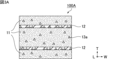
- FIG. 3A is a schematic cross-sectional view showing an example of crystal distribution in the glass ceramic structure of FIG.
- FIG. 3B is a schematic cross-sectional view showing another example of the crystal distribution in the glass ceramic structure of FIG.
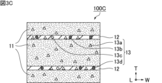
- FIG. 3C is a schematic cross-sectional view showing another example of the crystal distribution in the glass ceramic structure of FIG.
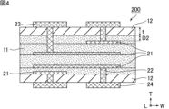
- FIG. 4 is a schematic cross-sectional view showing an example of the second glass-ceramic structure.
- FIG. 5 is a schematic cross-sectional view showing an example of an electronic component.
- FIG. 5 is a schematic cross-sectional view showing an example of an electronic component.
- FIG. 6 is a perspective view showing a method for measuring the bending strength of the glass ceramic structures produced in the examples.
- FIG. 7 is a schematic cross-sectional view for evaluating the strength of the glass ceramic structures produced in the examples.
- FIG. 8 is a schematic cross-sectional view for evaluating the strength of the glass ceramic structure produced in the example.
- the first glass ceramic structure, the second glass ceramic structure, and the electronic component of the present invention will be described below. Note that the present invention is not limited to the following configurations, and may be modified as appropriate without departing from the gist of the present invention. In addition, a combination of multiple individual preferred configurations described below also constitutes the present invention.
- the first glass ceramic structure of the present invention has a first ceramic layer containing crystals, and a second ceramic layer containing crystals and having a different crystal content from that of the first ceramic layer, and the second ceramic layer is present between the first ceramic layers in the thickness direction or on the surface of the glass ceramic structure.
- the first ceramic layer is a main body.
- Figure 1 is a schematic cross-sectional view showing an example of a first glass ceramic structure.
- the glass ceramic structure 100 shown in Figure 1 is formed by laminating three first ceramic layers 11 and two second ceramic layers 12.
- the second ceramic layer 12 having a layer thickness t ( ⁇ m) is arranged at a position with the shortest distance D1 from one main surface 100a of the glass ceramic structure 100, and another second ceramic layer 12 is arranged at a position with the shortest distance D1 from the other main surface 100b of the glass ceramic structure 100.
- the second ceramic layer may be two layers, one layer, or three or more layers. It is preferable that the first glass ceramic structure has two second ceramic layers.
- the relationship between the shortest distance in the thickness direction from the surface of the first glass ceramic structure to the second ceramic layer (hereinafter sometimes referred to as the "shortest distance from the surface") and the layer thickness of the second ceramic layer is (shortest distance from the surface)/(layer thickness of the second ceramic layer) ⁇ 10.
- the shortest distance from the surface and the thickness of the second ceramic layer are determined as follows. As shown in Fig. 1, first, a cross section (WT cross section) in the width (W) and stacking (T) directions passing through the center of the length (L) direction of the glass ceramic structure is exposed by polishing. If necessary, an etching treatment is performed on the polished surface. Then, the exposed cross section is observed by a scanning electron microscope.
- the interval between adjacent straight lines may be determined to be approximately 5 to 10 times the layer thickness of the second ceramic layer to be measured.
- draw the same number of straight lines on both sides of straight line Lc In other words, draw an odd number of straight lines including straight lines Lc. For example, draw three straight lines including straight lines Lc.
- FIG. 2 is a schematic cross-sectional view showing another example of a first glass-ceramic structure, in which two second ceramic layers 12 are disposed on two main surfaces of a glass-ceramic structure 110.
- the shortest distance in the thickness direction from the surface of the first glass ceramic structure to the second ceramic layer is, for example, preferably 0 ⁇ m or more and 150 ⁇ m or less, and more preferably 0 ⁇ m or more and 120 ⁇ m or less.
- the thickness of the second ceramic layer is, for example, preferably 3 ⁇ m or more and 75 ⁇ m or less, and more preferably 5 ⁇ m or more and 60 ⁇ m or less.
- the shortest distance and the thickness of the second ceramic layer are not limited to the above ranges, and may be adjusted to satisfy the above formula.
- the thickness of the second ceramic layer is preferably 3 ⁇ m or more and 75 ⁇ m or less.
- the composition of the first ceramic layer is as follows: SiO2 : 45% to 77.5% by weight , B2O3 : 5% to 20% by weight, Al2O3 : 2.6% to 20% by weight, ZnO : 2.7% to 20% by weight, CuO: 0% to 3.4% by weight, BaO: 0% to 10% by weight.
- the above compositions are calculated as oxides.
- the second ceramic layer (also called the crystalline layer) has a non-crystalline portion with a composition in the same range as the composition of the first ceramic layer described above, but has a different crystalline content from the first ceramic layer, with the second ceramic layer containing more crystals.
- the type of crystal with a different content is not particularly limited, and may be crystals contained in the first ceramic layer, or crystals not contained in the first ceramic layer but only in the second ceramic layer, or both.
- Examples of the crystals contained in the first ceramic layer include Al 2 O 3 and ZnO.
- Examples of crystals contained only in the second ceramic layer include ZnSi2O4 , ZnAl2O4 , BaAl2Si2O8 , ZnTiO3 , Al2TiO5 , TiO2 , Mg2SiO4 , MgSiO3 , and MgO .
- the crystals having different contents between the first ceramic layer and the second ceramic layer are at least one selected from the group consisting of Al2O3 , ZnSi2O4 , ZnO, ZnAl2O4 , BaAl2Si2O8 , ZnTiO3 , Al2TiO5 , TiO2 , Mg2SiO4 , MgSiO3 , and MgO .
- the crystals having different contents may be one type or two or more types, but are preferably two or more types.
- the proportion of the cross-sectional area of the crystals present in the second ceramic layer in the ceramic cross section is greater than the proportion of the cross-sectional area of the crystals present in the first ceramic layer in the ceramic cross section, and the difference (hereinafter sometimes referred to as difference (d1)) is 10 area % or more and 75 area % or less.
- the cross-sectional area of the crystals is not the cross-sectional area of a specific type of crystal, but the total cross-sectional area of all types of crystals. Since the difference (d1) is a comparison of the cross-sectional areas of all types of crystals, the proportion of a specific type of crystal in the second ceramic layer may be less than the proportion of the same specific type of crystal in the first ceramic layer.
- the proportion of the cross-sectional area of the crystals in the ceramic cross section can be calculated, for example, as follows. First, the cross section of the sample is observed using a scanning electron microscope (SEM) and an X-ray diffraction analyzer (XRD), and the crystalline and amorphous parts are marked with specific colors. The marked crystalline parts are extracted using image analysis software or image editing software (Photoshop (registered trademark), ImageJ, etc.), and after black and white binarization processing, the cross-sectional areas of the crystalline parts and the amorphous parts are obtained. The cross-sectional area of the crystalline parts is divided by the sum of the cross-sectional areas of the crystalline parts and the amorphous parts to calculate the proportion of the cross-sectional area of the crystals in the ceramic cross section.
- SEM scanning electron microscope
- XRD X-ray diffraction analyzer
- the difference (d1) is 10 area % or more and 75 area % or less, the flexural strength of the glass ceramic structure is improved compared to when the difference (d1) is outside the above range.
- Fig. 3A is a schematic cross-sectional view showing an example of crystal distribution in the glass ceramic structure of Fig. 1.
- Fig. 3B is a schematic cross-sectional view showing another example of crystal distribution in the glass ceramic structure of Fig. 1.
- Fig. 3C is a schematic cross-sectional view showing another example of crystal distribution in the glass ceramic structure of Fig. 1.
- the crystals 13a present in the second ceramic layer 12 are also present in the first ceramic layer 11, and the second ceramic layer 12 contains more crystals.
- the crystals 13a and 13b present in the second ceramic layer 12 are also present in the first ceramic layer 11, and the second ceramic layer 12 contains more crystals.
- the crystals 13b are not present in the first ceramic layer 11, and are present only in the second ceramic layer 12. If the difference (d1) is within the above range, the first ceramic layer 11 may contain more crystals 13a than the second ceramic layer 12, and the second ceramic layer 12 may not contain crystals 13a.
- the crystal 13a is also present in the first ceramic layer 11, and the second ceramic layer 12 contains more crystals.
- the crystals 13b, 13c, and 13d are not present in the first ceramic layer 11, and are present only in the second ceramic layer 12. If the difference (d1) is within the above range, the crystal 13a may be contained in greater amounts in the first ceramic layer 11 than in the second ceramic layer 12, and the crystal 13a may not be contained in the second ceramic layer 12.
- the only crystal present in the first ceramic layer 11 is crystal 13a, but two or more types of crystals may be present in the first ceramic layer 11. Also, four or more types of crystals may be present in the second ceramic layer 12.
- the first glass ceramic structure can be produced, for example, by the following method.
- (1) Preparation of Green Sheet A A glass ceramic material to be the first ceramic layer of the first glass ceramic structure is mixed with a binder, a plasticizer, etc. to prepare a ceramic slurry A.
- the ceramic slurry A is then formed on a substrate film (e.g., a polyethylene terephthalate (PET) film) and dried to prepare the green sheet A.
- a substrate film e.g., a polyethylene terephthalate (PET) film
- a mixed raw material is prepared by mixing the glass ceramic material used in the preparation of Green Sheet A with at least one filler component selected from the group consisting of Al2O3 , BaTiO3 , ZnO, and Mg2SiO4 .
- the mixed raw material is mixed with a binder, a plasticizer, etc. to prepare a ceramic slurry B. Then, the ceramic slurry B is formed on a substrate film and then dried to produce a green sheet B.
- Green sheets A are laminated, and green sheet B is placed on the surface of the laminate, or green sheet B is sandwiched between green sheets A to prepare a laminated green sheet, which is then fired to react green sheet A with green sheet B and generate crystals on the entire or part of the lamination surface of green sheet B.
- a second ceramic layer is formed at the position of green sheet B, and a glass ceramic structure (multilayer ceramic substrate) as shown in FIG. 1 or FIG. 2 is obtained.
- the crystals of Al 2 O 3 , BaAl 2 Si 2 O 8 and ZnAl 2 O 4 increase in the second ceramic layer.
- ZnO is used as the filler component
- Mg 2 SiO 4 is used as the filler component
- MgSiO 3 and MgO crystals increases in the second ceramic layer.
- BaTiO3 is used as the filler component, the crystals of ZnTiO3, Al2TiO5, BaAl2Si2O8 and TiO2 increase in the second ceramic layer.
- green sheet B it is also possible to form a pattern on green sheet A using ceramic slurry B, which is the raw material of green sheet B, and then stack the green sheet A with the pattern formed on it and sinter the resulting laminate to generate a second ceramic layer on the surface or inside of the glass ceramic structure.
- Methods for forming the pattern include metal mask printing, chemical etching using chemicals, physical etching such as laser processing, inkjet printing, spray coating, etc.
- the firing temperature of the laminated green sheets is not particularly limited as long as it is a temperature at which the glass ceramic material constituting green sheet A and green sheet B can be fired, and is, for example, 1000°C or less.
- the glass ceramic material used in the present invention is a low-temperature co-fired ceramic (LTCC) material.
- the laminated green sheets may be fired while sandwiched between constraining green sheets.
- the constraining green sheets contain, as a main component, an inorganic material (e.g., Al 2 O 3 ) that is not substantially fired at the firing temperature of the glass ceramic material constituting green sheets A and B. Therefore, the constraining green sheets do not shrink when the laminated green sheets are fired, and act to suppress shrinkage in the main surface direction of the laminated green sheets. As a result, the dimensional accuracy of the obtained structure is improved.
- the first glass ceramic structure has the above structure, which gives the location where the second ceramic layer is formed high fracture toughness.
- compressive stress and tensile stress can be generated in various locations within the second ceramic layer. This allows the stress to be distributed in response to a localized load, making it possible to increase fracture toughness.
- the second glass ceramic structure of the present invention is a glass ceramic structure having a plurality of first ceramic layers containing crystals, a second ceramic layer containing crystals and having a different crystal content from the first ceramic layers, and an internal electrode, wherein the second ceramic layer is present between the first ceramic layers in the thickness direction or on the surface of the glass ceramic structure, and the second ceramic layer and the internal electrode are adjacent to each other in the thickness direction, or the first ceramic layer is present between the second ceramic layer and the internal electrode in the thickness direction.
- the first ceramic layer is a main body.
- Figure 4 is a schematic cross-sectional view showing an example of a second glass ceramic structure.
- the glass ceramic structure 200 shown in Figure 4 is formed by laminating a plurality of first ceramic layers 11 and second ceramic layers 12 (four first ceramic layers and two second ceramic layers in Figure 4).
- the second ceramic layers 12 are present on the surface of the glass ceramic structure 200 in the thickness direction.
- the second ceramic layer may be two layers, one layer, or three or more layers. It is preferable that the second glass ceramic structure has two second ceramic layers.
- the internal electrodes 21 are arranged in multiple layers.
- the internal electrodes 21 are arranged between two first ceramic layers 11 adjacent in the thickness direction, or between the first ceramic layer 11 and the second ceramic layer 12 adjacent in the thickness direction.
- the second ceramic layer 12 having a layer thickness t ( ⁇ m) is arranged at the shortest distance D2 in the thickness direction from the internal electrode 21, and the first ceramic layer 11 is present between the second ceramic layer 12 and the internal electrode 21.
- Another second ceramic layer 12 is arranged so that a part of it is adjacent to the internal electrode 21 in the thickness direction.
- the glass ceramic structure 200 has via conductors 22 and external electrodes 23, 24 formed therein. These, for example, constitute passive elements such as capacitors and inductors, or constitute connection wiring that provides electrical connections between elements.
- the external electrode 23 is disposed on one main surface of the glass ceramic structure 200 .
- the external electrode 24 is disposed on the other main surface of the glass ceramic structure 200 .
- the via conductor 22 is arranged to penetrate the first ceramic layer 11 and the second ceramic layer 12, and serves to electrically connect the internal electrode 21 to the external electrodes 23 and 24.
- the via conductor 22 may be arranged to electrically connect two internal electrodes 21.
- the relationship between the shortest distance in the thickness direction from the internal electrode to the second ceramic layer and the layer thickness of the second ceramic layer is (shortest distance from the internal electrode)/(layer thickness of the second ceramic layer) ⁇ 10.
- the thickness of the second ceramic layer can be determined in the same manner as the first glass ceramic structure.
- the second ceramic layer is in contact with the internal electrode in the thickness direction.
- the shortest distance from the internal electrode to the second ceramic layer in the thickness direction is, for example, preferably 0 ⁇ m or more and 150 ⁇ m or less, and more preferably 0 ⁇ m or more and 120 ⁇ m or less.
- the thickness of the second ceramic layer is, for example, preferably 3 ⁇ m or more and 75 ⁇ m or less, and more preferably 5 ⁇ m or more and 60 ⁇ m or less.
- the shortest distance from the internal electrode and the thickness of the second ceramic layer are not limited to the above ranges, and may be adjusted to satisfy the above formula.
- the layer thickness of the second ceramic layer is preferably 3 ⁇ m or more and 75 ⁇ m or less.
- composition of the amorphous portion of the first ceramic layer and the second ceramic layer, the composition of the crystals, and the crystal content ratio can be the same as those of the first glass ceramic structure.
- the proportion of a cross-sectional area of the crystals present in the second ceramic layer in the ceramic cross section is greater than the proportion of a cross-sectional area of the crystals present in the first ceramic layer in the ceramic cross section, and the difference (d2) is 10 area % or more and 75 area % or less.
- the difference (d2) is 10 area % or more and 75 area % or less, structural defects occurring around the internal electrodes and their deterioration can be suppressed, compared to when the difference (d2) is outside the above range.
- the internal electrodes, via conductors, and external electrodes can be formed using a conductive paste containing Ag or Cu.
- the internal electrodes, via conductors, and external electrodes preferably contain Cu as the main component.
- the internal electrodes, via conductors, and external electrodes can be formed by printing using a metal mask or the like, or by transfer lamination of a Cu pattern.
- the second glass-ceramic structure can be produced, for example, by the following method.
- the green sheets A and B can be prepared in the same manner as the first glass ceramic structure.
- the internal electrodes, via conductors, and external electrodes are formed on a part of the green sheets A by using a conductive paste containing Ag or Cu or the like.
- a laminated green sheet is prepared by laminating green sheet A, and disposing green sheet B on the surface of the laminate, and then fired to react green sheet A with green sheet B, thereby forming crystals on the entire or part of the lamination surface of green sheet B.
- a glass ceramic structure as shown in FIG.
- the laminated green sheet is fired at 1000°C or less, in the same manner as in the preparation of the first glass ceramic structure.
- the firing atmosphere for the laminated green sheet is not particularly limited, but an air atmosphere is preferred when a material that is not easily oxidized, such as Ag, is used as the internal electrodes, and a low-oxygen atmosphere, such as a nitrogen atmosphere, is preferred when a material that is easily oxidized, such as Cu, is used.
- the firing atmosphere for the laminated green sheet may also be a reducing atmosphere.
- the second glass ceramic structure has the above structure, which gives the location where the second ceramic layer is formed high fracture toughness.
- the electronic component of the present invention includes the first glass-ceramic structure of the present invention and/or the second glass-ceramic structure of the present invention.
- the electronic component of the present invention includes, for example, a multilayer ceramic substrate, which is an example of a first glass ceramic structure and a second glass ceramic structure, and a chip component mounted on the multilayer ceramic substrate.
- the chip component include an LC filter, a capacitor, an inductor, a patch antenna, a coupler, and a laminated balun.
- FIG. 5 is a schematic cross-sectional view showing an example of an electronic component.
- a chip component 30 may be mounted on a glass ceramic structure (multilayer ceramic substrate) 200 in a state where it is electrically connected to an external electrode 23. In this way, an electronic component 300 including the glass ceramic structure 200 is formed.
- the electronic component 300 may be mounted on a mounting substrate (e.g., a motherboard) so as to be electrically connected via the external electrodes 24.
- a mounting substrate e.g., a motherboard
- the first glass ceramic structure and the second glass ceramic structure may also be applied to chip components mounted on a multilayer ceramic substrate. That is, the first glass ceramic structure and the second glass ceramic structure may be applied to an LC filter, a capacitor, an inductor, a patch antenna, a coupler, a laminated balun, etc.
- the first glass ceramic structure and the second glass ceramic structure may be applied to applications other than multilayer ceramic substrates and chip components.
- the first ceramic layer has a composition of SiO2 : 45% by weight or more and 77.5% by weight or less, B2O3 : 5% by weight or more and 20% by weight or less, Al2O3 : 2.6% by weight or more and 20% by weight or less, ZnO: 2.7% by weight or more and 20% by weight or less, CuO: 0% by weight or more and 3.4% by weight or less, BaO: 0% by weight or more and 10% by weight or less;
- the crystal is at least one selected from
- a glass ceramic structure having a plurality of first ceramic layers containing crystals, a second ceramic layer containing crystals and having a different crystal content from the first ceramic layers, and an internal electrode, the second ceramic layer is present between the first ceramic layers in a thickness direction or on a surface of the glass ceramic structure; the second ceramic layer and the internal electrode are adjacent to each other in a thickness direction, or the first ceramic layer is present between the second ceramic layer and the internal electrode in the thickness direction; a relationship between a shortest distance from the internal electrode to the second ceramic layer in a thickness direction and a layer thickness of the second ceramic layer is (shortest distance from the internal electrode)/(layer thickness of the second ceramic layer) ⁇ 10; the first ceramic layer has a composition of SiO2 : 45% by weight or more and 77.5% by weight or less, B2O3 : 5% by weight or more and 20% by weight or less, Al2O3 : 2.6% by weight or more and 20% by weight or less, ZnO: 2.7% by weight or more and 20% by weight or less
- the prepared mixed powder raw material was mixed with a toluene/ethanol mixed solvent and a dispersant, mixed in a ball mill with PSZ balls (diameter: 5 mm), and then a butyral-based binder solution and a plasticizer dissolved in a toluene/ethanol mixed solvent were added and further mixed to obtain the target slurry.
- the obtained slurry was molded on a carrier film with a doctor blade and dried to obtain a green sheet A with a thickness of 20 ⁇ m after firing.
- Green Sheets B1 to B4 A powder mixture was prepared by mixing 10% by weight or more and 95% by weight or less of the glass frit used in Green Sheet A with 5% by weight or more and 90% by weight or less of one of Al 2 O 3 (Green Sheet B1), ZnO (Green Sheet B2), Mg 2 SiO 4 (Green Sheet B3) or BaTiO 3 (Green Sheet B4) as a filler component.
- the prepared powder mixture was mixed in a ball mill with PSZ balls (diameter: 5 mm), and then a butyral-based binder solution and a plasticizer dissolved in a toluene/ethanol mixed solvent were added and further mixed to obtain the target slurry.
- the obtained slurry was formed on a carrier film with a doctor blade and dried to obtain green sheets B1 to B4 with thicknesses of 5, 10, and 50 ⁇ m after firing, respectively.
- (C) Preparation of glass ceramic structure The glass ceramic structure was prepared by the following procedure: 50 sheets of green sheet A cut to 78 mm ⁇ 58 mm were stacked, and two sheets of green sheet B1 cut to the same dimensions were stacked on the surface of the stack of green sheet A, or at a position 50 ⁇ m or 100 ⁇ m from the surface of the stack of green sheet A in the thickness direction.
- the laminate was subjected to isostatic pressing at 160 MPa to prepare a bonded body.
- the bonded body was cut into individual pieces of 35 mm x 6 mm, and then fired in a reducing atmosphere at 900°C or higher and 1000°C or lower for 60 minutes or more to obtain the intended glass ceramic structure (hereinafter also referred to as a sample). Samples were also prepared in the same manner using green sheets B2 to B4.
- the crystals of Al 2 O 3 , BaAl 2 Si 2 O 8 and ZnAl 2 O 4 were increased.
- the crystals of ZnAl 2 O 3 , ZnO and ZnSi 2 O 4 were increased.
- the crystals of Mg 2 SiO 4 , MgSiO 3 and MgO were increased.
- the crystals of ZnTiO3 , Al2TiO5 , BaAl2Si2O8 and TiO2 were increased.
- the flexural strength of samples in which the cross-sectional area of the crystals in the ceramic cross section was 5 area %, 10 area %, 40 area %, and 75 area % larger than that of the surrounding layers was measured and evaluated.
- the proportion of the cross-sectional area of the crystal was calculated as follows. First, the cross-section of the sample was observed by a scanning electron microscope (SEM), and the crystalline portion and the amorphous portion were marked with a specific color. The marked crystalline portion was extracted using image analysis software (ImageJ), and a black and white binarization process was performed, after which the cross-sectional area of the crystalline portion and the cross-sectional area of the amorphous portion were obtained. The cross-sectional area of the crystalline portion was divided by the sum of the cross-sectional areas of the crystalline portion and the amorphous portion to obtain the proportion of the cross-sectional area of the crystal in the cross-section of the sample.
- FIG. 6 is a perspective view showing a method for measuring the flexural strength of the glass ceramic structure prepared in the example.
- the effectiveness of green sheet B was judged to be present for samples in which the flexural strength ratio exceeded 120% when the flexural strength of a reference sample produced by laminating and firing only green sheet A was taken as 100%.
- Tables 1 to 4 show the increase in the cross-sectional area of the crystals in the second ceramic layer compared to the first ceramic layer, the thickness (t) of the second ceramic layer, the distance (D1) of the second ceramic layer from the sample surface, and the flexural strength ratio of the sample, (D1)/(t), for the sample using green sheet B1.
- Tables 2 to 4 show the results when green sheets B2 to B4 were used.
- green sheet A has a ceramic composition of compositions 2 to 7 shown in Table 5, if the crystal content of the second ceramic layer is 10 area % or more and 75 area % or less compared to the surrounding area, an improvement in the flexural strength of the sample was also confirmed.
- green sheet A was laminated on the internal electrodes to a thickness of 0 to 50 ⁇ m, and then green sheet B1, which would have a thickness of 5 ⁇ m, 10 ⁇ m or 50 ⁇ m after firing, was laminated, and finally 25 layers of green sheet A, which would have a thickness of 20 ⁇ m after firing, were laminated again to produce a laminate.
- the laminate was subjected to a hydrostatic press at 160 MPa to produce a bonded body.
- the bonded body was cut into individual pieces of 5 mm x 5 mm, and then fired in a reducing atmosphere at 900 to 1000 ° C for 60 minutes or more to obtain a ceramic structure having an internal electrode, which was used as a strength confirmation sample.
- Strength confirmation samples were also produced in the same manner using green sheets B2 to B4.
- FIG. 7 is a schematic cross-sectional view for evaluating the strength of the glass ceramic structure prepared in the example.
- FIG. 8 is a schematic cross-sectional view for evaluating the strength of the glass ceramic structure prepared in the example.
- the stamping generates a crack inside the ceramic, and this crack is defined as a fracture line BL.
- the fracture line BL extends from the stamped portion toward the internal electrode 21 or the second ceramic layer 12.
- Each sample (glass ceramic structure 200) was observed to see whether the fracture line BL reached the internal electrode 21.
- the same experiment was also carried out for a ceramic and internal electrode structure (Comparative Example 19) formed only with green sheet A without using green sheets B1 to B4. The results are shown in Table 6.
- the ceramic composition of the green sheet A used in Examples 61 to 92 and Comparative Examples 19 to 27 is composition 1 in Table 5. Even when the green sheet A has a ceramic composition of compositions 2 to 7 shown in Table 5, if the crystal content of the second ceramic layer is 10 area % or more and 75 area % or less compared to the first ceramic layer, the fracture line does not reach the internal electrode, as in Examples 61 to 92.
- Second ceramic layer 13a, 13b, 13c, 13d Crystal 21 Internal electrode 22 Via conductor 23, 24 External electrode 30 Chip component 100, 100A, 100B, 100C, 110 First glass ceramic structure 100a One main surface 100b of first glass ceramic structure Other main surface 200 Second glass ceramic structure 300 Electronic component t Layer thickness D1 of second ceramic layer Shortest distance D2 from surface Shortest distance BL from internal electrode Break lines F1 , F2 , F3 Support P Impact point Pb Probe
Landscapes
- Chemical & Material Sciences (AREA)
- Engineering & Computer Science (AREA)
- Ceramic Engineering (AREA)
- Materials Engineering (AREA)
- Organic Chemistry (AREA)
- Chemical Kinetics & Catalysis (AREA)
- Geochemistry & Mineralogy (AREA)
- General Chemical & Material Sciences (AREA)
- Life Sciences & Earth Sciences (AREA)
- Manufacturing & Machinery (AREA)
- Structural Engineering (AREA)
- Dispersion Chemistry (AREA)
- Crystallography & Structural Chemistry (AREA)
- Composite Materials (AREA)
- Inorganic Chemistry (AREA)
- Microelectronics & Electronic Packaging (AREA)
- Production Of Multi-Layered Print Wiring Board (AREA)
- Compositions Of Oxide Ceramics (AREA)
Abstract
ガラスセラミックス構造体100は、結晶13を含む第1セラミックス層11、及び、結晶13を含み、第1セラミックス層11と結晶13の含有量が異なる第2セラミックス層12を有するガラスセラミックス構造体100であって、第2セラミックス層12は、ガラスセラミックス構造体100の表面に存在するか、又は、厚み方向で第1セラミックス層11の間に存在し、ガラスセラミックス構造体100の表面から第2セラミックス層12までの厚み方向における最短距離D1と、第2セラミックス層12の層厚tとの関係が、(表面からの最短距離)/(第2セラミックス層の層厚)≦10であり、第1セラミックス層11の組成がSiO2:45重量%以上、77.5重量%以下、B2O3:5重量%以上、20重量%以下、Al2O3:2.6重量%以上、20重量%以下、ZnO:2.7重量%以上、20重量%以下、CuO:0重量%以上、3.4重量%以下、BaO:0重量%以上、10重量%以下であり、結晶13が、Al2O3、ZnSi2O4、ZnO、ZnAl2O4、BaAl2Si2O8、ZnTiO3、Al2TiO5、TiO2、Mg2SiO4、MgSiO3及びMgOからなる群から選択される少なくとも1種であり、第2セラミックス層12に存在する結晶13のセラミックス断面に占める断面積の割合が、第1セラミックス層11に存在する結晶13のセラミックス断面に占める断面積の割合より多く、その差が10面積%以上、75面積%以下である、ことを特徴とする。
Description
本発明は、ガラスセラミックス構造体及び電子部品に関する。
低温焼結セラミック材料は、比抵抗の比較的小さな低融点金属材料と同時焼成できるので、高周波特性に優れた多層セラミック基板を形成することができ、情報通信端末における高周波モジュール用の基板材料等として多用されている。
低温焼結セラミック材料としては、Al2O3等のセラミック材料にB2O3-SiO2系ガラス材料を混合したガラスセラミック複合系材料が一般的であるが、焼成時に揮発しやすいホウ素が含まれているため、得られる基板の組成がばらつきやすい。この問題を解決するために、ホウ素を含まない非ガラス系の低温焼結セラミック材料が提案されているが、このような低温焼結セラミック材料を焼結してなるセラミック焼結体は、破壊靱性値が小さいため、望ましい強度特性が得られないことがある。
特許文献1では、クォーツ(Quartz)、アルミナ(Alumina)、フレスノイト(Fresnoite)、サンボルナイト(Sanbornite)及びセルシアン(Celsian)の各結晶相を含み、粉末X線回析法により回析ピーク角度2θ=10~40°の範囲で測定した前記フレスノイトの(201)面における回折ピーク強度Aと前記クォーツの(110)面における回折ピーク強度Bの関係が、A/B≧2.5であることを特徴とするセラミック焼結体が開示されている。
特許文献1では、セラミックス層内にフレスノイトやセルシアン等の結晶を全体的に析出させることで、セラミック焼結体の強度が増加されている。しかしながら、構造全体に結晶が析出しているため、電気特性が一定程度に制限され、セラミック焼結体の特定の箇所に応力を付与することができない。また、特許文献1の焼結体は材料組成に特徴があるため、強度を付与するためには、ガラスセラミック材料の組成変更が必要である。
本発明は、上記課題を解決するものであり、局所的に破壊靭性が付与されたガラスセラミックス構造体及び電子部品を提供することを目的とする。
本発明の第一のガラスセラミックス構造体は、結晶を含む第1セラミックス層、及び、結晶を含み、上記第1セラミックス層と結晶の含有量が異なる第2セラミックス層を有するガラスセラミックス構造体であって、上記第2セラミックス層は、上記ガラスセラミックス構造体の表面に存在するか、又は、厚み方向で上記第1セラミックス層の間に存在し、上記ガラスセラミックス構造体の表面から上記第2セラミックス層までの厚み方向における最短距離と、上記第2セラミックス層の層厚との関係が、(表面からの最短距離)/(第2セラミックス層の層厚)≦10であり、上記第1セラミックス層の組成がSiO2:45重量%以上、77.5重量%以下、B2O3:5重量%以上、20重量%以下、Al2O3:2.6重量%以上、20重量%以下、ZnO:2.7重量%以上、20重量%以下、CuO:0重量%以上、3.4重量%以下、BaO:0重量%以上、10重量%以下であり、上記結晶が、Al2O3、ZnSi2O4、ZnO、ZnAl2O4、BaAl2Si2O8、ZnTiO3、Al2TiO5、TiO2、Mg2SiO4、MgSiO3及びMgOからなる群から選択される少なくとも1種であり、上記第2セラミックス層に存在する結晶のセラミックス断面に占める断面積の割合が、上記第1セラミックス層に存在する結晶のセラミックス断面に占める断面積の割合より多く、その差が10面積%以上、75面積%以下である、ことを特徴とする。
本発明の第二のガラスセラミックス構造体は、結晶を含む複数の第1セラミックス層、結晶を含み、上記第1セラミックス層と結晶の含有量が異なる第2セラミックス層、及び、内部電極を有するガラスセラミックス構造体であって、上記第2セラミックス層は、厚み方向で上記第1セラミックス層の間に存在するか、又は、前記ガラスセラミックス構造体の表面に存在し、上記第2セラミックス層と上記内部電極とは厚み方向で隣り合っているか、又は、厚み方向で上記第2セラミックス層と上記内部電極との間に上記第1セラミックス層が存在し、上記内部電極から上記第2セラミックス層までの厚み方向における最短距離と、上記第2セラミックス層の層厚との関係が、(内部電極からの最短距離)/(第2セラミックス層の層厚)≦10であり、上記第1セラミックス層の組成がSiO2:45重量%以上、77.5重量%以下、B2O3:5重量%以上、20重量%以下、Al2O3:2.6重量%以上、20重量%以下、ZnO:2.7重量%以上、20重量%以下、CuO:0重量%以上、3.4重量%以下、BaO:0重量%以上、10重量%以下であり、上記結晶が、Al2O3、ZnSi2O4、ZnO、ZnAl2O4、BaAl2Si2O8、ZnTiO3、Al2TiO5、TiO2、Mg2SiO4、MgSiO3及びMgOからなる群から選択される少なくとも1種であり、上記第2セラミックス層に存在する結晶のセラミックス断面に占める断面積の割合が、上記第1セラミックス層に存在する結晶のセラミックス断面に占める断面積の割合より多く、その差が10面積%以上、75面積%以下である、ことを特徴とする。
本発明の電子部品は、上記のガラスセラミックス構造体を含む。
本発明によれば、局所的に破壊靭性が付与されたガラスセラミックス構造体及び電子部品を提供することができる。
以下、本発明の第一のガラスセラミックス構造体、第二のガラスセラミックス構造体及び電子部品について説明する。なお、本発明は、以下の構成に限定されるものではなく、本発明の要旨を逸脱しない範囲において適宜変更されてもよい。また、以下において記載する個々の好ましい構成を複数組み合わせたものもまた本発明である。
本発明の第一のガラスセラミックス構造体は、結晶を含む第1セラミックス層、及び、結晶を含み、上記第1セラミックス層と結晶の含有量が異なる第2セラミックス層を有し、上記第2セラミックス層は、厚み方向で上記第1セラミックス層の間に存在するか、又は、上記ガラスセラミックス構造体の表面に存在する。
第一のガラスセラミックス構造体において、第1セラミックス層が主素体である。
第一のガラスセラミックス構造体において、第1セラミックス層が主素体である。
図1は、第一のガラスセラミックス構造体の一例を示す模式断面図である。図1に示すガラスセラミックス構造体100は、3層の第1セラミックス層11と、2層の第2セラミックス層12とが積層されてなる。図1では、層厚t(μm)の第2セラミックス層12が、ガラスセラミックス構造体100の一方主面100aから最短距離D1の位置に配置され、別の第2セラミックス層12が、ガラスセラミックス構造体100の他方主面100bから最短距離D1の位置に配置されている。
第2セラミックス層は2層であってもよいし、1層であってもよいし、3層以上であってもよい。第一のガラスセラミックス構造体は、第2セラミックス層を2層有することが好ましい。
第一のガラスセラミックス構造体の表面から上記第2セラミックス層までの厚み方向における最短距離(以下では「表面からの最短距離」と記載することがある)と、上記第2セラミックス層の層厚との関係が、(表面からの最短距離)/(第2セラミックス層の層厚)≦10である。上記式を満たすことにより、第一のガラスセラミックス構造体は、第2セラミックス層が形成された位置により高い破壊靭性が付与されている。
表面からの最短距離及び第2セラミックス層の層厚は、以下のようにして定める。
図1に示すように、まず、ガラスセラミックス構造体の長さ(L)方向の中心を通る、幅(W)方向及び積層(T)方向の断面(WT断面)を研磨により露出させる。必要に応じて、研磨面にエッチング処理を行う。そして、露出させた断面を走査型電子顕微鏡により観察する。
図1に示すように、まず、ガラスセラミックス構造体の長さ(L)方向の中心を通る、幅(W)方向及び積層(T)方向の断面(WT断面)を研磨により露出させる。必要に応じて、研磨面にエッチング処理を行う。そして、露出させた断面を走査型電子顕微鏡により観察する。
第1セラミックス層及び第2セラミックス層の積層方向Tに延びてかつガラスセラミックス構造体の中心を通る直線Lcを引く。次に、直線Lcと平行な複数の直線を等間隔に引く。隣り合う直線の間隔は、測定しようとする第2セラミックス層の層厚の5倍以上10倍以下程度で決めればよい。また、直線Lcの両側に同じ本数の直線を引く。すなわち、直線Lcを合わせて奇数本の直線を引く。例えば、直線Lcを合わせて3本の直線を引く。
次に、直線Lc等の各直線上において、表面からの最短距離及び第2セラミックス層の層厚をそれぞれ測定する。ただし、各直線上において、第2セラミックス層が欠損して、この第2セラミックス層を挟む第1セラミックス層同士が繋がっている場合、又は、測定位置の拡大像が不明瞭である場合は、更に直線Lcから離れた直線上において、表面からの最短距離及び第2セラミックス層の層厚をそれぞれ測定する。それぞれの平均値を、表面からの最短距離、第2セラミックス層の層厚とする。
第一のガラスセラミックス構造体の表面から第2セラミックス層までの厚み方向における最短距離(表面からの最短距離)が0であるとき、第2セラミックス層は第一のガラスセラミックス構造体の表面に存在する(図2)。
図2は、第一のガラスセラミックス構造体の別の一例を示す模式断面図である。図2では、2層の第2セラミックス層12がガラスセラミックス構造体110の2つの主面上に配置されている。
図2は、第一のガラスセラミックス構造体の別の一例を示す模式断面図である。図2では、2層の第2セラミックス層12がガラスセラミックス構造体110の2つの主面上に配置されている。
第一のガラスセラミックス構造体の表面から第2セラミックス層までの厚み方向における最短距離は、例えば0μm以上、150μm以下が好ましく、0μm以上、120μm以下がより好ましい。
第2セラミックス層の層厚は、例えば3μm以上、75μm以下が好ましく、5μm以上、60μm以下がより好ましい。
上記最短距離と第2セラミックス層の層厚は上記の範囲に限定されず、上記式を満たすように調整すればよい。なお、上記最短距離が0である、すなわち、第2セラミックス層が第一のガラスセラミックス構造体の表面に存在すると、(表面からの最短距離)/(第2セラミックス層の層厚)の値が第2セラミックス層の層厚に関係なく常に0になるが、その場合は、第2セラミックス層の層厚は、3μm以上、75μm以下が好ましい。
第2セラミックス層の層厚は、例えば3μm以上、75μm以下が好ましく、5μm以上、60μm以下がより好ましい。
上記最短距離と第2セラミックス層の層厚は上記の範囲に限定されず、上記式を満たすように調整すればよい。なお、上記最短距離が0である、すなわち、第2セラミックス層が第一のガラスセラミックス構造体の表面に存在すると、(表面からの最短距離)/(第2セラミックス層の層厚)の値が第2セラミックス層の層厚に関係なく常に0になるが、その場合は、第2セラミックス層の層厚は、3μm以上、75μm以下が好ましい。
上記第1セラミックス層の組成は、SiO2:45重量%以上、77.5重量%以下、B2O3:5重量%以上、20重量%以下、Al2O3:2.6重量%以上、20重量%以下、ZnO:2.7重量%以上、20重量%以下、CuO:0重量%以上、3.4重量%以下、BaO:0重量%以上、10重量%以下である。上記組成は、酸化物換算である。
第2セラミックス層(結晶層ともいう)は、非結晶部分が上述した第1セラミックス層の組成と同じ範囲の組成であるが、第1セラミックス層と結晶の含有量が異なっており、第2セラミックス層により多くの結晶が含まれている。含有量が異なっている結晶の種類は特に限定されず、第1セラミックス層に含まれる結晶であってもよいし、第1セラミックス層に含まれず第2セラミックス層のみに含まれる結晶であってもよいし、両方であってもよい。
第1セラミックス層に含まれる結晶としては、例えば、Al2O3、ZnO等が挙げられる。
第2セラミックス層にのみ含まれる結晶としては、例えば、ZnSi2O4、ZnAl2O4、BaAl2Si2O8、ZnTiO3、Al2TiO5、TiO2、Mg2SiO4、MgSiO3、MgO等が挙げられる。
第2セラミックス層にのみ含まれる結晶としては、例えば、ZnSi2O4、ZnAl2O4、BaAl2Si2O8、ZnTiO3、Al2TiO5、TiO2、Mg2SiO4、MgSiO3、MgO等が挙げられる。
第1セラミックス層と第2セラミックス層とで含有量が異なっている結晶は、Al2O3、ZnSi2O4、ZnO、ZnAl2O4、BaAl2Si2O8、ZnTiO3、Al2TiO5、TiO2、Mg2SiO4、MgSiO3及びMgOからなる群から選択される少なくとも1種である。含有量が異なっている結晶は、1種でもよいし、2種以上でもよいが、2種以上であることが好ましい。
第2セラミックス層に存在する結晶のセラミックス断面に占める断面積の割合は、第1セラミックス層に存在する結晶のセラミックス断面に占める断面積の割合より多く、その差(以下では差(d1)と記載することがある)が10面積%以上、75面積%以下である。ここで、結晶の断面積とは、特定の種類の結晶の断面積ではなく、全ての種類の結晶の断面積の合計である。上記差(d1)は、全ての種類の結晶の断面積の比較であるので、第2セラミックス層における特定の種類の結晶の割合が、第1セラミックス層における特定の同じ種類の結晶の割合より少なくなっていてもよい。
セラミックス断面に占める結晶の断面積の割合は、例えば、以下のようにして算出することができる。まず、走査型電子顕微鏡(SEM)及びX線回折分析装置(XRD)によって試料断面を観察し、結晶部位と非晶部位とを特定の色でマーキングする。画像解析ソフト又は画像編集ソフト(Photoshop(登録商標)、ImageJ等)を用いてマーキングを行った結晶部位を抽出し、白黒二値化処理を施したのち、結晶部位の断面積及び非晶部位の断面積を求める。結晶部位の断面積を、結晶部位の断面積及び非晶部位の断面積の合計で除すると、セラミックス断面に占める結晶の断面積の割合が算出される。
上記差(d1)が10面積%以上、75面積%以下であると、上記差(d1)が上記範囲外であるときと比較して、ガラスセラミックス構造体の抗折強度が向上する。
図3Aは、図1のガラスセラミックス構造体における結晶の分布の一例を示す模式断面図である。図3Bは、図1のガラスセラミックス構造体における結晶の分布の別の一例を示す模式断面図である。図3Cは、図1のガラスセラミックス構造体における結晶の分布の別の一例を示す模式断面図である。
図3Aのガラスセラミックス構造体100Aにおいて、第2セラミックス層12に存在する結晶13aは第1セラミックス層11にも存在し、第2セラミックス層12により多くの結晶が含まれている。
図3Aのガラスセラミックス構造体100Aにおいて、第2セラミックス層12に存在する結晶13aは第1セラミックス層11にも存在し、第2セラミックス層12により多くの結晶が含まれている。
図3Bのガラスセラミックス構造体100Bにおいて、第2セラミックス層12に存在する結晶13a、結晶13bのうち、結晶13aが第1セラミックス層11にも存在し、第2セラミックス層12により多くの結晶が含まれている。結晶13bは第1セラミックス層11には存在せず、第2セラミックス層12にのみ存在する。上記差(d1)が上記範囲であれば、結晶13aは、第2セラミックス層12より第1セラミックス層11により多く含まれていてもよいし、結晶13aは、第2セラミックス層12に含まれていなくてもよい。
図3Cのガラスセラミックス構造体100Cにおいて、第2セラミックス層12に存在する結晶13a、結晶13b、結晶13c及び結晶13dのうち、結晶13aが第1セラミックス層11にも存在し、第2セラミックス層12により多くの結晶が含まれている。結晶13b、結晶13c及び結晶13dは第1セラミックス層11には存在せず、第2セラミックス層12にのみ存在する。上記差(d1)が上記範囲であれば、結晶13aは、第2セラミックス層12より第1セラミックス層11により多く含まれていてもよいし、結晶13aは、第2セラミックス層12に含まれていなくてもよい。
図3A、図3B及び図3Cでは、第1セラミックス層11に存在する結晶が結晶13aのみであるが、第1セラミックス層11に2種以上の結晶が存在していてもよい。また、第2セラミックス層12には、4種以上の結晶が存在していてもよい。
第一のガラスセラミックス構造体は、例えば以下の方法により作製することができる。
(1)グリーンシートAの作製
第一のガラスセラミックス構造体の第1セラミックス層となるガラスセラミックス材料を、バインダ、可塑剤等と混合し、セラミックスラリーAを調製する。そして、セラミックスラリーAを基材フィルム(例えば、ポリエチレンテレフタレート(PET)フィルム)上に成形した後、乾燥させることによって、グリーンシートAを作製する。
(1)グリーンシートAの作製
第一のガラスセラミックス構造体の第1セラミックス層となるガラスセラミックス材料を、バインダ、可塑剤等と混合し、セラミックスラリーAを調製する。そして、セラミックスラリーAを基材フィルム(例えば、ポリエチレンテレフタレート(PET)フィルム)上に成形した後、乾燥させることによって、グリーンシートAを作製する。
(2)グリーンシートBの作製
グリーンシートAの作製に用いたガラスセラミックス材料と、Al2O3、BaTiO3、ZnO及びMg2SiO4からなる群から選択される少なくとも1つのフィラー成分とを混合して混合原料を作製する。混合原料中のフィラー成分の割合が高くなるほど、第2セラミックス層に析出する結晶が多くなるので、所望する結晶の割合に応じてフィラー成分の配合量を調整する。
混合原料をバインダ、可塑剤等と混合し、セラミックスラリーBを調製する。そして、セラミックスラリーBを基材フィルム上に成形した後、乾燥させることによって、グリーンシートBを作製する。
グリーンシートAの作製に用いたガラスセラミックス材料と、Al2O3、BaTiO3、ZnO及びMg2SiO4からなる群から選択される少なくとも1つのフィラー成分とを混合して混合原料を作製する。混合原料中のフィラー成分の割合が高くなるほど、第2セラミックス層に析出する結晶が多くなるので、所望する結晶の割合に応じてフィラー成分の配合量を調整する。
混合原料をバインダ、可塑剤等と混合し、セラミックスラリーBを調製する。そして、セラミックスラリーBを基材フィルム上に成形した後、乾燥させることによって、グリーンシートBを作製する。
(3)積層グリーンシートの作製及び焼成
グリーンシートAを積層し、積層体の表面にグリーンシートBを配置するか、又は、グリーンシートAでグリーンシートBを挟んで積層グリーンシートを作製し、焼成してグリーンシートAとグリーンシートBとを反応させ、結晶をグリーンシートBの積層面全体又は一部に生成させる。その結果、グリーンシートBの位置に第2セラミックス層が形成され、図1又は図2に示すようなガラスセラミックス構造体(多層セラミック基板)が得られる。
グリーンシートAを積層し、積層体の表面にグリーンシートBを配置するか、又は、グリーンシートAでグリーンシートBを挟んで積層グリーンシートを作製し、焼成してグリーンシートAとグリーンシートBとを反応させ、結晶をグリーンシートBの積層面全体又は一部に生成させる。その結果、グリーンシートBの位置に第2セラミックス層が形成され、図1又は図2に示すようなガラスセラミックス構造体(多層セラミック基板)が得られる。
フィラー成分としてAl2O3を用いた場合、第2セラミックス層ではAl2O3、BaAl2Si2O8及びZnAl2O4の結晶が増加する。
フィラー成分としてZnOを用いた場合、第2セラミックス層ではZnAl2O3、ZnO及びZnSi2O4の結晶が増加する。
フィラー成分としてMg2SiO4を用いた場合、第2セラミックス層ではMg2SiO4、MgSiO3及びMgOの結晶が増加する。
フィラー成分としてBaTiO3を用いた場合、第2セラミックス層ではZnTiO3、Al2TiO5、BaAl2Si2O8及びTiO2の結晶が増加する。
フィラー成分としてZnOを用いた場合、第2セラミックス層ではZnAl2O3、ZnO及びZnSi2O4の結晶が増加する。
フィラー成分としてMg2SiO4を用いた場合、第2セラミックス層ではMg2SiO4、MgSiO3及びMgOの結晶が増加する。
フィラー成分としてBaTiO3を用いた場合、第2セラミックス層ではZnTiO3、Al2TiO5、BaAl2Si2O8及びTiO2の結晶が増加する。
フィラー成分であるBaTiO3のBaを他のアルカリ土類金属に置き換えた化合物も、基本構造が同系の結晶が析出するため、代用可能である。
また、グリーンシートBを使用する以外に、グリーンシートA上にグリーンシートBの原料であるセラミックスラリーBでパターンを形成し、パターンが形成されたグリーンシートAを積層して得られた積層体を焼成することで、ガラスセラミックス構造体の表面又は内部に第2セラミックス層を生成させることも可能である。パターンの形成の方法としては、メタルマスク印刷、薬品を用いた化学エッチング、レーザー加工等の物理エッチング、インクジェット印刷、スプレー塗布等が挙げられる。
積層グリーンシートの焼成温度は、グリーンシートA及びグリーンシートBを構成するガラスセラミックス材料が焼成可能な温度であれば特に限定されず、例えば、1000℃以下である。本発明で用いるガラスセラミックス材料は、低温同時焼成セラミックス(LTCC)材料である。
なお、積層グリーンシートは、拘束用グリーンシートで挟まれた状態で焼成されてもよい。拘束用グリーンシートは、グリーンシートA及びグリーンシートBを構成するガラスセラミックス材料の焼成温度では実質的に焼成しない無機材料(例えば、Al2O3)を主成分として含有するものである。そのため、拘束用グリーンシートは、積層グリーンシートの焼成時に収縮せず、積層グリーンシートに対して主面方向での収縮を抑制するように作用する。その結果、得られる構造体の寸法精度が高まる。
第一のガラスセラミックス構造体は、上記の構造を有していることにより、第2セラミックス層が形成された位置により高い破壊靭性が付与されている。ガラスセラミックス構造体の厚み方向の表面又は厚み方向の表面に近い箇所の少なくとも一部に集中して結晶を析出させることで、圧縮応力と引張応力とを第2セラミックス層内各所に発生させることができる。これにより、局所的な負荷に対して応力が分散され、破壊靭性を強くすることが可能となる。
次に、第二のガラスセラミックス構造体について説明する。
本発明の第二のガラスセラミックス構造体は、結晶を含む複数の第1セラミックス層、結晶を含み、上記第1セラミックス層と結晶の含有量が異なる第2セラミックス層、及び、内部電極を有するガラスセラミックス構造体であって、上記第2セラミックス層は、厚み方向で上記第1セラミックス層の間に存在するか、又は、前記ガラスセラミックス構造体の表面に存在し、上記第2セラミックス層と上記内部電極とは厚み方向で隣り合っているか、又は、厚み方向で上記第2セラミックス層と上記内部電極との間に上記第1セラミックス層が存在する。
第二のガラスセラミックス構造体において、第1セラミックス層が主素体である。
本発明の第二のガラスセラミックス構造体は、結晶を含む複数の第1セラミックス層、結晶を含み、上記第1セラミックス層と結晶の含有量が異なる第2セラミックス層、及び、内部電極を有するガラスセラミックス構造体であって、上記第2セラミックス層は、厚み方向で上記第1セラミックス層の間に存在するか、又は、前記ガラスセラミックス構造体の表面に存在し、上記第2セラミックス層と上記内部電極とは厚み方向で隣り合っているか、又は、厚み方向で上記第2セラミックス層と上記内部電極との間に上記第1セラミックス層が存在する。
第二のガラスセラミックス構造体において、第1セラミックス層が主素体である。
図4は、第二のガラスセラミックス構造体の一例を示す模式断面図である。図4に示すガラスセラミックス構造体200は、第1セラミックス層11及び第2セラミックス層12が複数(図4では第1セラミックス層が4層、第2セラミックス層が2層)積層されてなる。第2セラミックス層12は、厚み方向でガラスセラミックス構造体200の表面に存在している。
第2セラミックス層は2層であってもよいし、1層であってもよいし、3層以上であってもよい。第二のガラスセラミックス構造体は、第2セラミックス層を2層有することが好ましい。
ガラスセラミックス構造体200には、内部電極21が複数層に配置されている。内部電極21は、厚み方向に隣接する2つの第1セラミックス層11の間に配置されているか、厚み方向に隣接する第1セラミックス層11と第2セラミックス層12との間に配置されている。図4では、層厚t(μm)の第2セラミックス層12が、内部電極21から厚み方向における最短距離D2の位置に配置され、第2セラミックス層12と内部電極21との間には、第1セラミックス層11が存在している。別の第2セラミックス層12は、一部が内部電極21と厚み方向で隣り合って配置されている。
ガラスセラミックス構造体200には、ビア導体22及び外部電極23、24が形成されている。これらは、例えば、コンデンサ、インダクタ等の受動素子を構成したり、素子間の電気的接続を担う接続配線を構成したりする。
外部電極23は、ガラスセラミックス構造体200の一方主面上に配置されている。
外部電極24は、ガラスセラミックス構造体200の他方主面上に配置されている。
外部電極24は、ガラスセラミックス構造体200の他方主面上に配置されている。
ビア導体22は、第1セラミックス層11及び第2セラミックス層12を貫通するように配置されており、内部電極21と外部電極23、24を電気的に接続する役割を担っている。ビア導体22は、2つの内部電極21を電気的に接続するように配置されていてもよい。
第二のガラスセラミックス構造体において、上記内部電極から上記第2セラミックス層までの厚み方向における最短距離と、上記第2セラミックス層の層厚との関係が、(内部電極からの最短距離)/(第2セラミックス層の層厚)≦10である。上記式を満たすことにより、第二のガラスセラミックス構造体は、第2セラミックス層が形成された位置により高い破壊靭性が付与されている。
第2セラミックス層の層厚は、第一のガラスセラミックス構造体と同様に定めることができる。
内部電極から第2セラミックス層までの厚み方向における最短距離(内部電極からの最短距離)が0であるとき、第2セラミックス層は厚み方向に内部電極と接している。
内部電極から第2セラミックス層までの厚み方向における最短距離は、例えば0μm以上、150μm以下が好ましく、0μm以上、120μm以下がより好ましい。
第2セラミックス層の層厚は、例えば3μm以上、75μm以下が好ましく、5μm以上、60μm以下がより好ましい。
内部電極からの最短距離と第2セラミックス層の層厚は上記の範囲に限定されず、上記式を満たすように調整すればよい。なお、上記最短距離が0である、すなわち、第2セラミックス層が内部電極に接していると、(内部電極からの最短距離)/(第2セラミックス層の層厚)の値が第2セラミックス層の層厚に関係なく常に0になるが、その場合は、第2セラミックス層の層厚は3μm以上、75μm以下が好ましい。
第2セラミックス層の層厚は、例えば3μm以上、75μm以下が好ましく、5μm以上、60μm以下がより好ましい。
内部電極からの最短距離と第2セラミックス層の層厚は上記の範囲に限定されず、上記式を満たすように調整すればよい。なお、上記最短距離が0である、すなわち、第2セラミックス層が内部電極に接していると、(内部電極からの最短距離)/(第2セラミックス層の層厚)の値が第2セラミックス層の層厚に関係なく常に0になるが、その場合は、第2セラミックス層の層厚は3μm以上、75μm以下が好ましい。
上記第1セラミックス層及び第2セラミックス層の非結晶部分の組成、結晶の組成及び結晶の含有割合は、第一のガラスセラミックス構造体と同様とすることができる。
第二のガラスセラミックス構造体において、第2セラミックス層に存在する結晶のセラミックス断面に占める断面積の割合は、第1セラミックス層に存在する結晶のセラミックス断面に占める断面積の割合より多く、その差(d2)が10面積%以上、75面積%以下である。
上記差(d2)が10面積%以上、75面積%以下であると、上記差(d2)が上記範囲外であるときと比較して、内部電極の周囲で発生する構造欠陥とその悪化を抑制することができる。
上記差(d2)が10面積%以上、75面積%以下であると、上記差(d2)が上記範囲外であるときと比較して、内部電極の周囲で発生する構造欠陥とその悪化を抑制することができる。
内部電極、ビア導体及び外部電極は、Ag又はCuを含む導電性ペーストを用いて形成することができる。第二のガラスセラミックス構造体において、内部電極、ビア導体及び外部電極は、主成分がCuであることが好ましい。内部電極、ビア導体及び外部電極は、メタルマスク等を用いた印刷や、Cuパターンを転写積層することで形成可能である。
第二のガラスセラミックス構造体は、例えば以下の方法により作製することができる。
グリーンシートAの作製及びグリーンシートBの作製は、第一のガラスセラミックス構造体の作製と同様に行うことができる。内部電極、ビア導体及び外部電極は、一部のグリーンシートAにAg又はCuを含む導電性ペースト等を用いて形成する。
グリーンシートAを積層し、積層体の表面にグリーンシートBを配置して積層グリーンシートを作製し、焼成してグリーンシートAとグリーンシートBとを反応させ、結晶をグリーンシートBの積層面全体又は一部に生成させる。その結果、図4に示すようなガラスセラミックス構造体が得られる。
グリーンシートAの作製及びグリーンシートBの作製は、第一のガラスセラミックス構造体の作製と同様に行うことができる。内部電極、ビア導体及び外部電極は、一部のグリーンシートAにAg又はCuを含む導電性ペースト等を用いて形成する。
グリーンシートAを積層し、積層体の表面にグリーンシートBを配置して積層グリーンシートを作製し、焼成してグリーンシートAとグリーンシートBとを反応させ、結晶をグリーンシートBの積層面全体又は一部に生成させる。その結果、図4に示すようなガラスセラミックス構造体が得られる。
積層グリーンシートの焼成は、第一のガラスセラミックス構造体の作製と同様に、1000℃以下で行う。積層グリーンシートの焼成雰囲気は、特に限定されないが、内部電極等として、Ag等の酸化しにくい材料を用いる場合には空気雰囲気が好ましく、Cu等の酸化しやすい材料を用いる場合には窒素雰囲気等の低酸素雰囲気が好ましい。また、積層グリーンシートの焼成雰囲気は、還元雰囲気であってもよい。
第二のガラスセラミックス構造体は、上記の構造を有していることにより、第2セラミックス層が形成された位置により高い破壊靭性が付与されている。内部電極付近又は内部電極に隣接して第2セラミックス層を配置することで、第1セラミックス層に内部破断などの構造欠陥が発生した際に、クラックが内部電極へ延伸することを阻止し、回路短絡や断線などの信頼性の低下を抑制することができる。
次に、本発明の電子部品について説明する。
本発明の電子部品は、本発明の第一のガラスセラミックス構造体及び/又は本発明の第二のガラスセラミックス構造体を含む。
本発明の電子部品は、本発明の第一のガラスセラミックス構造体及び/又は本発明の第二のガラスセラミックス構造体を含む。
本発明の電子部品は、例えば、第一のガラスセラミックス構造体及び第二のガラスセラミックス構造体の一例である多層セラミック基板と、上記多層セラミック基板に搭載されたチップ部品と、を備える。チップ部品としては、例えば、LCフィルタ、コンデンサ、インダクタ、パッチアンテナ、カプラ、積層バラン等が挙げられる。
図5は電子部品の一例を示す模式断面図である。図5に示すように、ガラスセラミックス構造体(多層セラミック基板)200には、外部電極23と電気的に接続された状態で、チップ部品30が搭載されていてもよい。これにより、ガラスセラミックス構造体200を備える電子部品300が構成される。
電子部品300は、外部電極24を介して電気的に接続されるように、実装基板(例えば、マザーボード)に実装されてもよい。
以上では、第二のガラスセラミックス構造体が多層セラミック基板に適用される例を示したが、第一のガラスセラミックス構造体及び第二のガラスセラミックス構造体は、多層セラミック基板に搭載されるチップ部品に適用されてもよい。すなわち、第一のガラスセラミックス構造体及び第二のガラスセラミックス構造体は、LCフィルタ、コンデンサ、インダクタ、パッチアンテナ、カプラ、積層バラン等に適用されてもよい。
第一のガラスセラミックス構造体及び第二のガラスセラミックス構造体は、多層セラミック基板及びチップ部品以外に適用されてもよい。
本明細書には、以下の内容が開示されている。
<1>
結晶を含む第1セラミックス層、及び、結晶を含み、上記第1セラミックス層と結晶の含有量が異なる第2セラミックス層を有するガラスセラミックス構造体であって、
上記第2セラミックス層は、厚み方向で上記第1セラミックス層の間に存在するか、又は、上記ガラスセラミックス構造体の表面に存在し、
上記ガラスセラミックス構造体の表面から上記第2セラミックス層までの厚み方向における最短距離と、上記第2セラミックス層の層厚との関係が、(表面からの最短距離)/(第2セラミックス層の層厚)≦10であり、
上記第1セラミックス層の組成がSiO2:45重量%以上、77.5重量%以下、B2O3:5重量%以上、20重量%以下、Al2O3:2.6重量%以上、20重量%以下、ZnO:2.7重量%以上、20重量%以下、CuO:0重量%以上、3.4重量%以下、BaO:0重量%以上、10重量%以下であり、
上記結晶が、Al2O3、ZnSi2O4、ZnO、ZnAl2O4、BaAl2Si2O8、ZnTiO3、Al2TiO5、TiO2、Mg2SiO4、MgSiO3及びMgOからなる群から選択される少なくとも1種であり、
上記第2セラミックス層に存在する結晶のセラミックス断面に占める断面積の割合が、上記第1セラミックス層に存在する結晶のセラミックス断面に占める断面積の割合より多く、その差が10面積%以上、75面積%以下である、ことを特徴とするガラスセラミックス構造体。
結晶を含む第1セラミックス層、及び、結晶を含み、上記第1セラミックス層と結晶の含有量が異なる第2セラミックス層を有するガラスセラミックス構造体であって、
上記第2セラミックス層は、厚み方向で上記第1セラミックス層の間に存在するか、又は、上記ガラスセラミックス構造体の表面に存在し、
上記ガラスセラミックス構造体の表面から上記第2セラミックス層までの厚み方向における最短距離と、上記第2セラミックス層の層厚との関係が、(表面からの最短距離)/(第2セラミックス層の層厚)≦10であり、
上記第1セラミックス層の組成がSiO2:45重量%以上、77.5重量%以下、B2O3:5重量%以上、20重量%以下、Al2O3:2.6重量%以上、20重量%以下、ZnO:2.7重量%以上、20重量%以下、CuO:0重量%以上、3.4重量%以下、BaO:0重量%以上、10重量%以下であり、
上記結晶が、Al2O3、ZnSi2O4、ZnO、ZnAl2O4、BaAl2Si2O8、ZnTiO3、Al2TiO5、TiO2、Mg2SiO4、MgSiO3及びMgOからなる群から選択される少なくとも1種であり、
上記第2セラミックス層に存在する結晶のセラミックス断面に占める断面積の割合が、上記第1セラミックス層に存在する結晶のセラミックス断面に占める断面積の割合より多く、その差が10面積%以上、75面積%以下である、ことを特徴とするガラスセラミックス構造体。
<2>
上記結晶が2種以上である、<1>に記載のガラスセラミックス構造体。
上記結晶が2種以上である、<1>に記載のガラスセラミックス構造体。
<3>
上記第2セラミックス層を2層有する、<1>又は<2>に記載のガラスセラミックス構造体。
上記第2セラミックス層を2層有する、<1>又は<2>に記載のガラスセラミックス構造体。
<4>
結晶を含む複数の第1セラミックス層、結晶を含み、上記第1セラミックス層と結晶の含有量が異なる第2セラミックス層、及び、内部電極を有するガラスセラミックス構造体であって、
上記第2セラミックス層は、厚み方向で上記第1セラミックス層の間に存在するか、又は、前記ガラスセラミックス構造体の表面に存在し、
上記第2セラミックス層と上記内部電極とは厚み方向で隣り合っているか、又は、厚み方向で上記第2セラミックス層と上記内部電極との間に上記第1セラミックス層が存在し、
上記内部電極から上記第2セラミックス層までの厚み方向における最短距離と、上記第2セラミックス層の層厚との関係が、(内部電極からの最短距離)/(第2セラミックス層の層厚)≦10であり、
上記第1セラミックス層の組成がSiO2:45重量%以上、77.5重量%以下、B2O3:5重量%以上、20重量%以下、Al2O3:2.6重量%以上、20重量%以下、ZnO:2.7重量%以上、20重量%以下、CuO:0重量%以上、3.4重量%以下、BaO:0重量%以上、10重量%以下であり、
上記結晶が、Al2O3、ZnSi2O4、ZnO、ZnAl2O4、BaAl2Si2O8、ZnTiO3、Al2TiO5、TiO2、Mg2SiO4、MgSiO3及びMgOからなる群から選択される少なくとも1種であり、
上記第2セラミックス層に存在する結晶のセラミックス断面に占める断面積の割合が、上記第1セラミックス層に存在する結晶のセラミックス断面に占める断面積の割合より多く、その差が10面積%以上、75面積%以下である、ことを特徴とする、ガラスセラミックス構造体。
結晶を含む複数の第1セラミックス層、結晶を含み、上記第1セラミックス層と結晶の含有量が異なる第2セラミックス層、及び、内部電極を有するガラスセラミックス構造体であって、
上記第2セラミックス層は、厚み方向で上記第1セラミックス層の間に存在するか、又は、前記ガラスセラミックス構造体の表面に存在し、
上記第2セラミックス層と上記内部電極とは厚み方向で隣り合っているか、又は、厚み方向で上記第2セラミックス層と上記内部電極との間に上記第1セラミックス層が存在し、
上記内部電極から上記第2セラミックス層までの厚み方向における最短距離と、上記第2セラミックス層の層厚との関係が、(内部電極からの最短距離)/(第2セラミックス層の層厚)≦10であり、
上記第1セラミックス層の組成がSiO2:45重量%以上、77.5重量%以下、B2O3:5重量%以上、20重量%以下、Al2O3:2.6重量%以上、20重量%以下、ZnO:2.7重量%以上、20重量%以下、CuO:0重量%以上、3.4重量%以下、BaO:0重量%以上、10重量%以下であり、
上記結晶が、Al2O3、ZnSi2O4、ZnO、ZnAl2O4、BaAl2Si2O8、ZnTiO3、Al2TiO5、TiO2、Mg2SiO4、MgSiO3及びMgOからなる群から選択される少なくとも1種であり、
上記第2セラミックス層に存在する結晶のセラミックス断面に占める断面積の割合が、上記第1セラミックス層に存在する結晶のセラミックス断面に占める断面積の割合より多く、その差が10面積%以上、75面積%以下である、ことを特徴とする、ガラスセラミックス構造体。
<5>
上記結晶が2種以上である、<4>に記載のガラスセラミックス構造体。
上記結晶が2種以上である、<4>に記載のガラスセラミックス構造体。
<6>
上記第2セラミックス層を2層有し、上記内部電極が厚み方向で上記第2セラミックス層の間に存在する、<4>又は<5>に記載のガラスセラミックス構造体。
上記第2セラミックス層を2層有し、上記内部電極が厚み方向で上記第2セラミックス層の間に存在する、<4>又は<5>に記載のガラスセラミックス構造体。
<7>
<1>~<6>のいずれかに記載のガラスセラミックス構造体を含む電子部品。
<1>~<6>のいずれかに記載のガラスセラミックス構造体を含む電子部品。
以下、本発明のガラスセラミックス構造体をより具体的に開示した実施例を示す。なお、本発明は、これらの実施例のみに限定されるものではない。
(ガラスセラミックス構造体の作製)
(A)グリーンシートAの作製
B2O3/SiO2/Al2O3/ZnO/CuOを組成とするガラスフリットにSiO2クォーツ粉末を混合し、焼成後組成として酸化物換算でSiO2が74.21重量%、B2O3が10.76重量%、Al2O3が6.03重量%、ZnOが6.02重量%、CuOが0.47重量%、BaOが2.50重量%となる混合粉末原料を調製した(表5の組成1)。
調製した混合粉末原料をトルエン/エタノール混合溶媒及び分散剤と混合させ、PSZボール(直径:5mm)とともにボールミルで混合し、更にトルエン/エタノール混合溶媒で溶解したブチラール系バインダ溶液及び可塑剤を添加して、更に混合することで、目的とするスラリーを得た。得られたスラリーをドクターブレードでキャリアフィルム上に成形し、乾燥することで、焼成後の厚みが20μmとなるグリーンシートAを得た。
(A)グリーンシートAの作製
B2O3/SiO2/Al2O3/ZnO/CuOを組成とするガラスフリットにSiO2クォーツ粉末を混合し、焼成後組成として酸化物換算でSiO2が74.21重量%、B2O3が10.76重量%、Al2O3が6.03重量%、ZnOが6.02重量%、CuOが0.47重量%、BaOが2.50重量%となる混合粉末原料を調製した(表5の組成1)。
調製した混合粉末原料をトルエン/エタノール混合溶媒及び分散剤と混合させ、PSZボール(直径:5mm)とともにボールミルで混合し、更にトルエン/エタノール混合溶媒で溶解したブチラール系バインダ溶液及び可塑剤を添加して、更に混合することで、目的とするスラリーを得た。得られたスラリーをドクターブレードでキャリアフィルム上に成形し、乾燥することで、焼成後の厚みが20μmとなるグリーンシートAを得た。
(B)グリーンシートB1~B4の作製
グリーンシートAで用いたガラスフリットを10重量%以上、95重量%以下、フィラー成分としてAl2O3(グリーンシートB1)、ZnO(グリーンシートB2)、Mg2SiO4(グリーンシートB3)又はBaTiO3(グリーンシートB4)のいずれか1種を5重量%以上、90重量%以下混合した粉末混合物を調製した。
調製した粉末混合物をPSZボール(直径:5mm)とともにボールミルで混合し、更にトルエン/エタノール混合溶媒で溶解したブチラール系バインダ溶液及び可塑剤を添加して、更に混合することで、目的とするスラリーを得た。得られたスラリーをドクターブレードでキャリアフィルム上に成形し、乾燥することで、グリーンシートB1~B4のそれぞれについて、焼成後厚みが5、10、50μmとなるグリーンシートを得た。
グリーンシートAで用いたガラスフリットを10重量%以上、95重量%以下、フィラー成分としてAl2O3(グリーンシートB1)、ZnO(グリーンシートB2)、Mg2SiO4(グリーンシートB3)又はBaTiO3(グリーンシートB4)のいずれか1種を5重量%以上、90重量%以下混合した粉末混合物を調製した。
調製した粉末混合物をPSZボール(直径:5mm)とともにボールミルで混合し、更にトルエン/エタノール混合溶媒で溶解したブチラール系バインダ溶液及び可塑剤を添加して、更に混合することで、目的とするスラリーを得た。得られたスラリーをドクターブレードでキャリアフィルム上に成形し、乾燥することで、グリーンシートB1~B4のそれぞれについて、焼成後厚みが5、10、50μmとなるグリーンシートを得た。
(C)ガラスセラミックス構造体の作製
ガラスセラミックス構造体は以下の手順で作製した。78mm×58mmにカットしたグリーンシートAを50枚積層し、同じ寸法にカットした2枚のグリーンシートB1をグリーンシートAの積層体の表面に積層するか、又は、グリーンシートAの積層体の表面から厚み方向50μm又は100μmの位置に積層した。
上記積層体について160MPaで静水圧プレスを行い、圧着体を作製した。圧着体を35mm×6mmの個片にカットした後に、還元雰囲気中にて900℃以上、1000℃以下で60分間以上焼成を行うことで、目的とするガラスセラミックス構造体(以下、試料とも記載する)を得た。グリーンシートB2~B4を用いた場合についても同様に、試料を作製した。
ガラスセラミックス構造体は以下の手順で作製した。78mm×58mmにカットしたグリーンシートAを50枚積層し、同じ寸法にカットした2枚のグリーンシートB1をグリーンシートAの積層体の表面に積層するか、又は、グリーンシートAの積層体の表面から厚み方向50μm又は100μmの位置に積層した。
上記積層体について160MPaで静水圧プレスを行い、圧着体を作製した。圧着体を35mm×6mmの個片にカットした後に、還元雰囲気中にて900℃以上、1000℃以下で60分間以上焼成を行うことで、目的とするガラスセラミックス構造体(以下、試料とも記載する)を得た。グリーンシートB2~B4を用いた場合についても同様に、試料を作製した。
(D)ガラスセラミックス構造体の断面観察
ブレードダイシングを用いて、上記で作製した試料の断面を露出させた。エネルギー分散型X線分析(EDX)及びX線回折(XRD)を用い、グリーンシートB1~B4のいずれかを積層した箇所近傍において、層状に結晶含有量が異なる層が観察された。結晶含有量が異なる層において、グリーンシートAを積層した箇所に対して含有量が変化している結晶、及び/又は、グリーンシートAを積層した箇所には存在せず、結晶含有量が異なる層にのみ析出している結晶が観察された。
ブレードダイシングを用いて、上記で作製した試料の断面を露出させた。エネルギー分散型X線分析(EDX)及びX線回折(XRD)を用い、グリーンシートB1~B4のいずれかを積層した箇所近傍において、層状に結晶含有量が異なる層が観察された。結晶含有量が異なる層において、グリーンシートAを積層した箇所に対して含有量が変化している結晶、及び/又は、グリーンシートAを積層した箇所には存在せず、結晶含有量が異なる層にのみ析出している結晶が観察された。
グリーンシートB1を用いた試料においては、Al2O3、BaAl2Si2O8及びZnAl2O4の結晶が増加していた。
グリーンシートB2を用いた試料においては、ZnAl2O3、ZnO及びZnSi2O4の結晶が増加していた。
グリーンシートB3を用いた試料においては、Mg2SiO4、MgSiO3及びMgOの結晶が増加していた。
グリーンシートB4を用いた試料においては、ZnTiO3、Al2TiO5、BaAl2Si2O8及びTiO2の結晶が増加していた。
グリーンシートB2を用いた試料においては、ZnAl2O3、ZnO及びZnSi2O4の結晶が増加していた。
グリーンシートB3を用いた試料においては、Mg2SiO4、MgSiO3及びMgOの結晶が増加していた。
グリーンシートB4を用いた試料においては、ZnTiO3、Al2TiO5、BaAl2Si2O8及びTiO2の結晶が増加していた。
セラミックス断面に占める結晶の断面積の割合が、周囲の層に比べ5面積%、10面積%、40面積%、75面積%多くなっている試料について、抗折強度を測定して評価した。
結晶の断面積の割合は、以下のようにして算出した。まず走査型電子顕微鏡(SEM)によって試料断面を観察し、結晶部位と非晶部位を特定の色でマーキングした。画像解析ソフト(ImageJ)を用いてマーキングを行った結晶部位を抽出し、白黒二値化処理を施したのち、結晶部位の断面積及び非晶部位の断面積を求めた。結晶部位の断面積を、結晶部位の断面積及び非晶部位の断面積の合計で除することにより、結晶の試料断面に占める断面積の割合を求めた。
結晶の断面積の割合は、以下のようにして算出した。まず走査型電子顕微鏡(SEM)によって試料断面を観察し、結晶部位と非晶部位を特定の色でマーキングした。画像解析ソフト(ImageJ)を用いてマーキングを行った結晶部位を抽出し、白黒二値化処理を施したのち、結晶部位の断面積及び非晶部位の断面積を求めた。結晶部位の断面積を、結晶部位の断面積及び非晶部位の断面積の合計で除することにより、結晶の試料断面に占める断面積の割合を求めた。
(E)抗折強度の測定
上記と同様の手順で長さ35mm×幅6mm×厚み0.6mmの抗折強度測定用の試料を作製し、抗折強度を測定した。具体的には、図6に示すように2点の支点F2、F3で試料(ガラスセラミックス構造体100)を下側から支えつつ、試料の中心部にプローブPbを降下させ、破断したときの押下圧力を抗折強度とした。支点F1とF2の距離、支点F1とF3の距離は、いずれも20mmとし、押下速度は1mm/minであった。測定はオートグラフAGX-5kNX(島津製作所社製)を用いて行った。図6は、実施例で作製したガラスセラミックス構造体の抗折強度を測定する方法を示す斜視図である。
グリーンシートAのみを積層、焼成して作製された参考試料の抗折強度を100%とした場合の抗折強度比が120%を超えた試料に関して、グリーンシートBの効果ありと判断した。結果を表1~4に示す。
表1にグリーンシートB1を用いた試料の、第1セラミックス層と比較した第2セラミックス層における結晶の断面積の増加割合、第2セラミックス層の層厚(t)、第2セラミックス層の試料表面からの距離(D1)、試料の抗折強度の比、(D1)/(t)を示す。
表1と同様に、表2~4にグリーンシートB2~B4を用いた場合の結果を示す。
上記と同様の手順で長さ35mm×幅6mm×厚み0.6mmの抗折強度測定用の試料を作製し、抗折強度を測定した。具体的には、図6に示すように2点の支点F2、F3で試料(ガラスセラミックス構造体100)を下側から支えつつ、試料の中心部にプローブPbを降下させ、破断したときの押下圧力を抗折強度とした。支点F1とF2の距離、支点F1とF3の距離は、いずれも20mmとし、押下速度は1mm/minであった。測定はオートグラフAGX-5kNX(島津製作所社製)を用いて行った。図6は、実施例で作製したガラスセラミックス構造体の抗折強度を測定する方法を示す斜視図である。
グリーンシートAのみを積層、焼成して作製された参考試料の抗折強度を100%とした場合の抗折強度比が120%を超えた試料に関して、グリーンシートBの効果ありと判断した。結果を表1~4に示す。
表1にグリーンシートB1を用いた試料の、第1セラミックス層と比較した第2セラミックス層における結晶の断面積の増加割合、第2セラミックス層の層厚(t)、第2セラミックス層の試料表面からの距離(D1)、試料の抗折強度の比、(D1)/(t)を示す。
表1と同様に、表2~4にグリーンシートB2~B4を用いた場合の結果を示す。


表1~4に示すように、結晶の増加割合が10面積%以上、75面積%以下で、かつ、(表面からの最短距離)/(第2セラミックス層の層厚)≦10である試料は、第2セラミックス層のない参照試料に対し、20%以上の抗折強度の向上が確認された。これは、ガラス等の非晶質に対し強度の強い結晶が局所的に存在することで、局所的に破壊靭性が付与されて強度が上がり、膨張係数の異なる物質が混ざりあうことで外部からかかる応力が分散されるためと考えられる。セラミックス構造体の表面からの距離が延びると強度が落ちる理由に関しては、応力の印加点と第2セラミックス層との間に、何も強化していない領域が増えていくためと考えられる。
グリーンシートAが表5に示す組成2~7のセラミックス組成である場合も、第2セラミックス層の結晶の含有量が周囲と比べ10面積%以上、75面積%以下である場合、同様に試料の抗折強度の向上が確認された。

(内部電極を有するセラミックス構造体の作製)
(A)グリーンシートAの作製
焼成後の厚みが5~50μmとなるように厚みを変更する以外は、上記と同様にグリーンシートAを得た。
(A)グリーンシートAの作製
焼成後の厚みが5~50μmとなるように厚みを変更する以外は、上記と同様にグリーンシートAを得た。
(B)グリーンシートB1~B4の作製
上記と同様にグリーンシートB1~B4を得た。
上記と同様にグリーンシートB1~B4を得た。
(C)強度確認用試料の作製
焼成後の厚みが20μmとなるグリーンシートAを25層積層し、その上に焼成後の厚みが5μm、10μm又は50μmとなるグリーンシートB1を積層した。その後、グリーンシートAを0~50μmの間で任意の厚みで積層し、その上に、焼成後の厚さ50μmとなる内部電極(Cu)を形成した。内部電極の形成には、スクリーン版を用いたスクリーン印刷を行った。具体的には、マスク上にCuペーストを適量配置し、マスクとグリーンシートを接触させた。その後Cuペーストをスキージングにより伸ばし、マスク開口よりグリーンシート上にCuペーストを印刷した。
更に内部電極の上にグリーンシートAを0~50μmの厚さで積層した後、焼成後の厚みが5μm、10μm又は50μmとなるグリーンシートB1を積層し、最後に再び焼成後の厚みが20μmとなるグリーンシートAを25層積層し、積層体を作製した。
上記積層体について160MPaで静水圧プレスを行い、圧着体を作製した。圧着体を5mm×5mmの個片にカットした後に、還元雰囲気中にて900~1000℃で60分間以上焼成を行うことで、内部電極を有するセラミックス構造体を得、これを強度確認用試料とした。グリーンシートB2~B4を用いた場合についても同様に、強度確認用試料を作製した。
焼成後の厚みが20μmとなるグリーンシートAを25層積層し、その上に焼成後の厚みが5μm、10μm又は50μmとなるグリーンシートB1を積層した。その後、グリーンシートAを0~50μmの間で任意の厚みで積層し、その上に、焼成後の厚さ50μmとなる内部電極(Cu)を形成した。内部電極の形成には、スクリーン版を用いたスクリーン印刷を行った。具体的には、マスク上にCuペーストを適量配置し、マスクとグリーンシートを接触させた。その後Cuペーストをスキージングにより伸ばし、マスク開口よりグリーンシート上にCuペーストを印刷した。
更に内部電極の上にグリーンシートAを0~50μmの厚さで積層した後、焼成後の厚みが5μm、10μm又は50μmとなるグリーンシートB1を積層し、最後に再び焼成後の厚みが20μmとなるグリーンシートAを25層積層し、積層体を作製した。
上記積層体について160MPaで静水圧プレスを行い、圧着体を作製した。圧着体を5mm×5mmの個片にカットした後に、還元雰囲気中にて900~1000℃で60分間以上焼成を行うことで、内部電極を有するセラミックス構造体を得、これを強度確認用試料とした。グリーンシートB2~B4を用いた場合についても同様に、強度確認用試料を作製した。
(D)強度確認試験
ブレードダイシングを用いて、上記で作製した強度確認用試料の断面を露出させた。D2=100の場合、図7に示すように、断面に観察される内部電極21から厚み方向に約20μmの位置(打点P)に、ビッカース硬度計(マツザワ製)を用いて50gfにて打刻した。図7は、実施例で作製したガラスセラミックス構造体の強度を評価する模式断面図である。D2=0の場合、図8に示すように、断面に観察される内部電極21から幅方向に約20μmの位置(打点P)に、D2=100の場合と同様に打刻した。図8は、実施例で作製したガラスセラミックス構造体の強度を評価する模式断面図である。
打刻によりセラミックス内部にクラックが発生するが、このクラックを破断線BLと定義した。打刻がセラミックスの強度を超える負荷の場合、打刻箇所から内部電極21や第2セラミックス層12に向けて破断線BLが延びるが、各試料(ガラスセラミックス構造体200)について、破断線BLが内部電極21に到達するか否かを観察した。
なお、グリーンシートB1~B4を使用しないでグリーンシートAのみで形成されたセラミックスと内部電極の構造体(比較例19)に関しても、同様の実験をした。結果を表6に示す。
ブレードダイシングを用いて、上記で作製した強度確認用試料の断面を露出させた。D2=100の場合、図7に示すように、断面に観察される内部電極21から厚み方向に約20μmの位置(打点P)に、ビッカース硬度計(マツザワ製)を用いて50gfにて打刻した。図7は、実施例で作製したガラスセラミックス構造体の強度を評価する模式断面図である。D2=0の場合、図8に示すように、断面に観察される内部電極21から幅方向に約20μmの位置(打点P)に、D2=100の場合と同様に打刻した。図8は、実施例で作製したガラスセラミックス構造体の強度を評価する模式断面図である。
打刻によりセラミックス内部にクラックが発生するが、このクラックを破断線BLと定義した。打刻がセラミックスの強度を超える負荷の場合、打刻箇所から内部電極21や第2セラミックス層12に向けて破断線BLが延びるが、各試料(ガラスセラミックス構造体200)について、破断線BLが内部電極21に到達するか否かを観察した。
なお、グリーンシートB1~B4を使用しないでグリーンシートAのみで形成されたセラミックスと内部電極の構造体(比較例19)に関しても、同様の実験をした。結果を表6に示す。
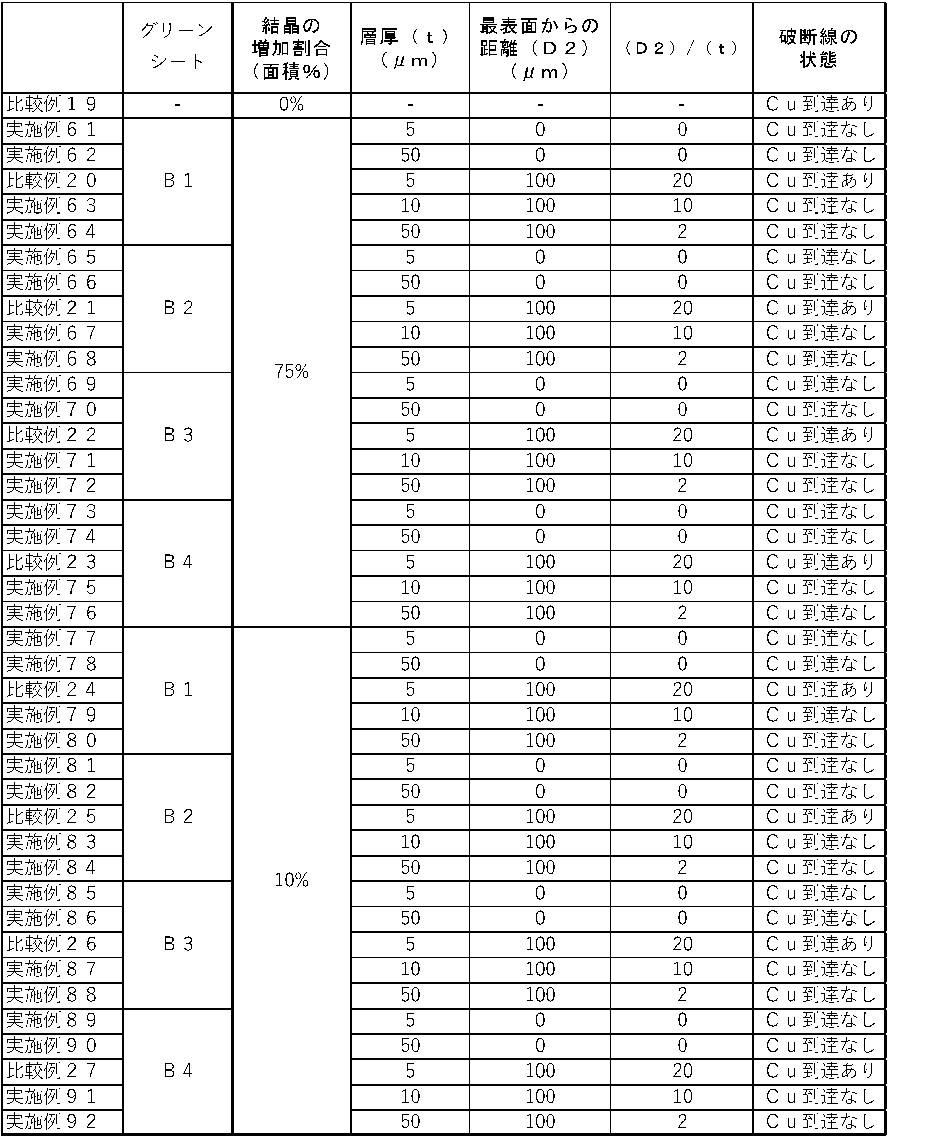
表6に示すように、第2セラミックス層を有していない比較例19、及び、(内部電極からの最短距離)/(第2セラミックス層の層厚)が20である比較例20~27では、破断線が内部電極まで到達していたが、(内部電極からの最短距離)/(第2セラミックス層の層厚)≦10を満たす実施例61~92では、破断線が内部電極まで到達しなかった。実施例61~92のセラミックス構造体は、実施例1~60のセラミックス構造体と同様に、ガラス等の非晶質に対し強度の強い結晶が局所的に存在することで局所的に破壊靭性が付与されて強度が上がり、膨張係数の異なる物質が混ざりあうことで外部からかかる応力が分散されると考えられる。上記のことから、構造欠陥が起きた場合、ヒートサイクル試験等を通しても内部電極へのクラック延伸を阻止することができ、回路短絡や断線等の信頼性の低下を防止することができる。
実施例61~92及び比較例19~27で使用したグリーンシートAのセラミックス組成は表5における組成1である。グリーンシートAが表5に示す組成2~7のセラミックス組成である場合も、第2セラミックス層の結晶の含有量が第1セラミックス層と比べ10面積%以上、75面積%以下であると、実施例61~92と同様に破断線が内部電極まで到達しなかった。
11 第1セラミックス層
12 第2セラミックス層
13、13a、13b、13c、13d 結晶
21 内部電極
22 ビア導体
23、24 外部電極
30 チップ部品
100、100A、100B、100C、110 第一のガラスセラミックス構造体
100a 第一のガラスセラミックス構造体の一方主面
100b 第一のガラスセラミックス構造体の他方主面
200 第二のガラスセラミックス構造体
300 電子部品
t 第2セラミックス層の層厚
D1 表面からの最短距離
D2 内部電極からの最短距離
BL 破断線
F1、F2、F3 支点
P 打点
Pb プローブ
12 第2セラミックス層
13、13a、13b、13c、13d 結晶
21 内部電極
22 ビア導体
23、24 外部電極
30 チップ部品
100、100A、100B、100C、110 第一のガラスセラミックス構造体
100a 第一のガラスセラミックス構造体の一方主面
100b 第一のガラスセラミックス構造体の他方主面
200 第二のガラスセラミックス構造体
300 電子部品
t 第2セラミックス層の層厚
D1 表面からの最短距離
D2 内部電極からの最短距離
BL 破断線
F1、F2、F3 支点
P 打点
Pb プローブ
Claims (7)
- 結晶を含む第1セラミックス層、及び、結晶を含み、前記第1セラミックス層と結晶の含有量が異なる第2セラミックス層を有するガラスセラミックス構造体であって、
前記第2セラミックス層は、厚み方向で前記第1セラミックス層の間に存在するか、又は、前記ガラスセラミックス構造体の表面に存在し、
前記ガラスセラミックス構造体の表面から前記第2セラミックス層までの厚み方向における最短距離と、前記第2セラミックス層の層厚との関係が、(表面からの最短距離)/(第2セラミックス層の層厚)≦10であり、
前記第1セラミックス層の組成がSiO2:45重量%以上、77.5重量%以下、B2O3:5重量%以上、20重量%以下、Al2O3:2.6重量%以上、20重量%以下、ZnO:2.7重量%以上、20重量%以下、CuO:0重量%以上、3.4重量%以下、BaO:0重量%以上、10重量%以下であり、
前記結晶が、Al2O3、ZnSi2O4、ZnO、ZnAl2O4、BaAl2Si2O8、ZnTiO3、Al2TiO5、TiO2、Mg2SiO4、MgSiO3及びMgOからなる群から選択される少なくとも1種であり、
前記第2セラミックス層に存在する結晶のセラミックス断面に占める断面積の割合が、前記第1セラミックス層に存在する結晶のセラミックス断面に占める断面積の割合より多く、その差が10面積%以上、75面積%以下である、ことを特徴とするガラスセラミックス構造体。 - 前記結晶が2種以上である、請求項1に記載のガラスセラミックス構造体。
- 前記第2セラミックス層を2層有する、請求項1又は2に記載のガラスセラミックス構造体。
- 結晶を含む複数の第1セラミックス層、結晶を含み、前記第1セラミックス層と結晶の含有量が異なる第2セラミックス層、及び、内部電極を有するガラスセラミックス構造体であって、
前記第2セラミックス層は、厚み方向で前記第1セラミックス層の間に存在するか、又は、前記ガラスセラミックス構造体の表面に存在し、
前記第2セラミックス層と前記内部電極とは厚み方向で隣り合っているか、又は、厚み方向で前記第2セラミックス層と前記内部電極との間に前記第1セラミックス層が存在し、
前記内部電極から前記第2セラミックス層までの厚み方向における最短距離と、前記第2セラミックス層の層厚との関係が、(内部電極からの最短距離)/(第2セラミックス層の層厚)≦10であり、
前記第1セラミックス層の組成がSiO2:45重量%以上、77.5重量%以下、B2O3:5重量%以上、20重量%以下、Al2O3:2.6重量%以上、20重量%以下、ZnO:2.7重量%以上、20重量%以下、CuO:0重量%以上、3.4重量%以下、BaO:0重量%以上、10重量%以下であり、
前記結晶が、Al2O3、ZnSi2O4、ZnO、ZnAl2O4、BaAl2Si2O8、ZnTiO3、Al2TiO5、TiO2、Mg2SiO4、MgSiO3及びMgOからなる群から選択される少なくとも1種であり、
前記第2セラミックス層に存在する結晶のセラミックス断面に占める断面積の割合が、前記第1セラミックス層に存在する結晶のセラミックス断面に占める断面積の割合より多く、その差が10面積%以上、75面積%以下である、ことを特徴とする、ガラスセラミックス構造体。 - 前記結晶が2種以上である、請求項4に記載のガラスセラミックス構造体。
- 前記第2セラミックス層を2層有し、前記内部電極が厚み方向で前記第2セラミックス層の間に存在する、請求項4又は5に記載のガラスセラミックス構造体。
- 請求項1~6のいずれか一項に記載のガラスセラミックス構造体を含む電子部品。
Priority Applications (3)
| Application Number | Priority Date | Filing Date | Title |
|---|---|---|---|
| JP2025527835A JP7861922B2 (ja) | 2023-06-16 | 2024-05-31 | ガラスセラミックス構造体及び電子部品 |
| CN202480006161.3A CN120418214A (zh) | 2023-06-16 | 2024-05-31 | 玻璃陶瓷结构体和电子部件 |
| US19/254,349 US20250326684A1 (en) | 2023-06-16 | 2025-06-30 | Glass ceramic structure and electronic component |
Applications Claiming Priority (2)
| Application Number | Priority Date | Filing Date | Title |
|---|---|---|---|
| JP2023099457 | 2023-06-16 | ||
| JP2023-099457 | 2023-06-16 |
Related Child Applications (1)
| Application Number | Title | Priority Date | Filing Date |
|---|---|---|---|
| US19/254,349 Continuation US20250326684A1 (en) | 2023-06-16 | 2025-06-30 | Glass ceramic structure and electronic component |
Publications (1)
| Publication Number | Publication Date |
|---|---|
| WO2024257630A1 true WO2024257630A1 (ja) | 2024-12-19 |
Family
ID=93851830
Family Applications (1)
| Application Number | Title | Priority Date | Filing Date |
|---|---|---|---|
| PCT/JP2024/020069 Ceased WO2024257630A1 (ja) | 2023-06-16 | 2024-05-31 | ガラスセラミックス構造体及び電子部品 |
Country Status (3)
| Country | Link |
|---|---|
| US (1) | US20250326684A1 (ja) |
| CN (1) | CN120418214A (ja) |
| WO (1) | WO2024257630A1 (ja) |
Citations (5)
| Publication number | Priority date | Publication date | Assignee | Title |
|---|---|---|---|---|
| JP2008270741A (ja) * | 2007-03-27 | 2008-11-06 | Kyocera Corp | 配線基板 |
| JP2011114173A (ja) * | 2009-11-27 | 2011-06-09 | Kyocera Corp | ガラスセラミック配線基板およびコイル内蔵ガラスセラミック配線基板ならびにガラスセラミック配線基板の製造方法 |
| WO2013099944A1 (ja) * | 2011-12-27 | 2013-07-04 | 株式会社村田製作所 | 多層セラミック基板およびそれを用いた電子部品 |
| WO2021256408A1 (ja) * | 2020-06-17 | 2021-12-23 | 株式会社村田製作所 | ガラス、ガラスセラミックス及び積層セラミック電子部品 |
| WO2023095605A1 (ja) * | 2021-11-25 | 2023-06-01 | 株式会社村田製作所 | ガラスセラミックス及び電子部品 |
-
2024
- 2024-05-31 WO PCT/JP2024/020069 patent/WO2024257630A1/ja not_active Ceased
- 2024-05-31 CN CN202480006161.3A patent/CN120418214A/zh active Pending
-
2025
- 2025-06-30 US US19/254,349 patent/US20250326684A1/en active Pending
Patent Citations (5)
| Publication number | Priority date | Publication date | Assignee | Title |
|---|---|---|---|---|
| JP2008270741A (ja) * | 2007-03-27 | 2008-11-06 | Kyocera Corp | 配線基板 |
| JP2011114173A (ja) * | 2009-11-27 | 2011-06-09 | Kyocera Corp | ガラスセラミック配線基板およびコイル内蔵ガラスセラミック配線基板ならびにガラスセラミック配線基板の製造方法 |
| WO2013099944A1 (ja) * | 2011-12-27 | 2013-07-04 | 株式会社村田製作所 | 多層セラミック基板およびそれを用いた電子部品 |
| WO2021256408A1 (ja) * | 2020-06-17 | 2021-12-23 | 株式会社村田製作所 | ガラス、ガラスセラミックス及び積層セラミック電子部品 |
| WO2023095605A1 (ja) * | 2021-11-25 | 2023-06-01 | 株式会社村田製作所 | ガラスセラミックス及び電子部品 |
Also Published As
| Publication number | Publication date |
|---|---|
| CN120418214A (zh) | 2025-08-01 |
| US20250326684A1 (en) | 2025-10-23 |
| JPWO2024257630A1 (ja) | 2024-12-19 |
Similar Documents
| Publication | Publication Date | Title |
|---|---|---|
| JP6214930B2 (ja) | 多層配線基板 | |
| CN209962815U (zh) | 层叠线圈部件 | |
| JP5821975B2 (ja) | 複合積層セラミック電子部品 | |
| JP5435176B2 (ja) | 複合積層セラミック電子部品 | |
| US7790271B2 (en) | Dielectric ceramic composition, ceramic substrate, and method for producing the same | |
| JP5761341B2 (ja) | ガラスセラミック組成物 | |
| EP2168928B1 (en) | Glass Ceramic Substrate | |
| WO2010092970A1 (ja) | 低温焼結セラミック焼結体および多層セラミック基板 | |
| JP7494908B2 (ja) | ガラスセラミックス及び積層セラミック電子部品 | |
| US20180319129A1 (en) | Multilayer body and electronic component | |
| JP5888524B2 (ja) | 複合積層セラミック電子部品 | |
| KR20100014344A (ko) | 적층 유전체 제조 방법 | |
| WO2010058697A1 (ja) | ガラスセラミック組成物およびガラスセラミック基板 | |
| KR20040008094A (ko) | 동 페이스트, 이것을 이용한 배선기판 및 배선기판의제조방법 | |
| JP7861922B2 (ja) | ガラスセラミックス構造体及び電子部品 | |
| US20250326684A1 (en) | Glass ceramic structure and electronic component | |
| JP7056764B2 (ja) | ガラスセラミック材料、積層体、及び、電子部品 | |
| JP6493560B2 (ja) | 多層セラミック基板及び電子部品 | |
| JP2005268712A (ja) | 積層セラミック電子部品およびその製造方法 |
Legal Events
| Date | Code | Title | Description |
|---|---|---|---|
| 121 | Ep: the epo has been informed by wipo that ep was designated in this application |
Ref document number: 24823250 Country of ref document: EP Kind code of ref document: A1 |
|
| WWE | Wipo information: entry into national phase |
Ref document number: 202480006161.3 Country of ref document: CN |
|
| WWE | Wipo information: entry into national phase |
Ref document number: 2025527835 Country of ref document: JP |
|
| WWP | Wipo information: published in national office |
Ref document number: 202480006161.3 Country of ref document: CN |
|
| NENP | Non-entry into the national phase |
Ref country code: DE |