WO2024257502A1 - 検出装置 - Google Patents
検出装置 Download PDFInfo
- Publication number
- WO2024257502A1 WO2024257502A1 PCT/JP2024/016776 JP2024016776W WO2024257502A1 WO 2024257502 A1 WO2024257502 A1 WO 2024257502A1 JP 2024016776 W JP2024016776 W JP 2024016776W WO 2024257502 A1 WO2024257502 A1 WO 2024257502A1
- Authority
- WO
- WIPO (PCT)
- Prior art keywords
- insulating film
- film
- inorganic
- organic
- substrate
- Prior art date
- Legal status (The legal status is an assumption and is not a legal conclusion. Google has not performed a legal analysis and makes no representation as to the accuracy of the status listed.)
- Pending
Links
Images


Classifications
-
- H—ELECTRICITY
- H10—SEMICONDUCTOR DEVICES; ELECTRIC SOLID-STATE DEVICES NOT OTHERWISE PROVIDED FOR
- H10K—ORGANIC ELECTRIC SOLID-STATE DEVICES
- H10K30/00—Organic devices sensitive to infrared radiation, light, electromagnetic radiation of shorter wavelength or corpuscular radiation
- H10K30/60—Organic devices sensitive to infrared radiation, light, electromagnetic radiation of shorter wavelength or corpuscular radiation in which radiation controls flow of current through the devices, e.g. photoresistors
-
- H—ELECTRICITY
- H10—SEMICONDUCTOR DEVICES; ELECTRIC SOLID-STATE DEVICES NOT OTHERWISE PROVIDED FOR
- H10K—ORGANIC ELECTRIC SOLID-STATE DEVICES
- H10K30/00—Organic devices sensitive to infrared radiation, light, electromagnetic radiation of shorter wavelength or corpuscular radiation
- H10K30/80—Constructional details
- H10K30/88—Passivation; Containers; Encapsulations
-
- H—ELECTRICITY
- H10—SEMICONDUCTOR DEVICES; ELECTRIC SOLID-STATE DEVICES NOT OTHERWISE PROVIDED FOR
- H10K—ORGANIC ELECTRIC SOLID-STATE DEVICES
- H10K39/00—Integrated devices, or assemblies of multiple devices, comprising at least one organic radiation-sensitive element covered by group H10K30/00
- H10K39/30—Devices controlled by radiation
- H10K39/32—Organic image sensors
Definitions
- the present invention relates to a detection device.
- Optical sensors capable of detecting fingerprint patterns and vein patterns are known (for example, see Patent Document 1). Such optical sensors have multiple photodiodes (OPD: Organic Photodiodes) that use an organic semiconductor material as the active layer. As described in Patent Document 2, the photodiodes are stacked in the following order: a lower electrode, an electron transport layer, an active layer, a hole transport layer, and an upper electrode. The electron transport layer or the hole transport layer is also called a buffer layer.
- OPD Organic Photodiodes
- the detection accuracy may decrease.
- the present invention aims to provide a detection device that can prevent moisture from entering.
- the detection device of one embodiment of the present invention comprises a substrate, an inorganic insulating film, an organic insulating film, and a barrier film stacked on the substrate, an organic photosensor stacked in the detection region of the substrate in the order of a lower electrode, a lower buffer layer, an active layer, an upper buffer layer, and an upper electrode, and a first inorganic sealing film covering the organic photosensor, and in the detection region, the inorganic insulating film, the organic insulating film, the barrier film, the organic photosensor, and the first inorganic sealing film are stacked in that order, and in the peripheral region outside the detection region, the inorganic insulating film, the organic insulating film, the barrier film, and the first inorganic sealing film are stacked in that order, and on the outer edge side of the substrate, the side of the organic insulating film and the side of the inorganic insulating film are located closer to the detection region than the side of the substrate, and the side of the organic insulating film and the side of the inorganic
- a detection device includes a substrate, an inorganic insulating film, an organic insulating film, and a barrier film stacked on the substrate, an organic photosensor stacked in the detection region of the substrate in the order of a lower electrode, a lower buffer layer, an active layer, an upper buffer layer, and an upper electrode, and a first inorganic sealing film covering the organic photosensor.
- the inorganic insulating film, the organic insulating film, the barrier film, the organic photosensor, and the first inorganic sealing film are stacked in that order, and in a peripheral region outside the detection region, the inorganic insulating film, the organic insulating film, the barrier film, and the first inorganic sealing film are stacked in that order, and in the peripheral region, the organic insulating film is formed on the upper surface of the organic insulating film and has a plurality of grooves extending along the outer edge of the substrate in a plan view.
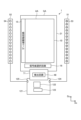
- FIG. 1 is a plan view that illustrates a detection device according to an embodiment.
- FIG. 2 is a block diagram illustrating an example of the configuration of the detection device according to the embodiment.
- FIG. 3 is a circuit diagram showing a detection device according to an embodiment.
- FIG. 4 is a plan view showing a schematic diagram of a plurality of photodiodes in the detection region and a plurality of grooves in the peripheral region.
- FIG. 5 is a cross-sectional view taken along line V-V' of FIG.
- FIG. 6 is a cross-sectional view taken along line VI-VI' of FIG.
- FIG. 7 is a cross-sectional view that illustrates a detection device according to a comparative example.
- FIG. 8 is a plan view showing a schematic diagram of the detection device before the outer shape is cut.
- FIG. 9 is a cross-sectional view taken along line IX-IX' of FIG.
- the term "on top” is used, unless otherwise specified, to include both a case in which another structure is placed directly on top of a structure so as to be in contact with the structure, and a case in which another structure is placed above a structure via yet another structure.
- Fig. 1 is a plan view showing a detection device according to an embodiment.
- the detection device 1 has a substrate 21, a sensor unit 10, a gate line driving circuit 15, a signal line selection circuit 16, a detection circuit 48, a control circuit 122, a power supply circuit 123, a first light source substrate 51, a second light source substrate 52, and light sources 53 and 54.
- a plurality of light sources 53 are provided on the first light source substrate 51.
- a plurality of light sources 54 are provided on the second light source substrate 52.
- the control board 121 is electrically connected to the board 21 via the wiring board 71.
- the wiring board 71 is, for example, a flexible printed circuit board or a rigid board.
- the detection circuit 48 is provided on the wiring board 71.
- the control board 121 is provided with a control circuit 122 and a power supply circuit 123.
- the control circuit 122 is, for example, an FPGA (Field Programmable Gate Array).
- the control circuit 122 supplies control signals to the sensor unit 10, the gate line driving circuit 15, and the signal line selection circuit 16 to control the detection operation of the sensor unit 10.
- the control circuit 122 also supplies control signals to the light sources 53 and 54 to control the lighting or non-lighting of the light sources 53 and 54.
- the power supply circuit 123 supplies voltage signals such as a sensor power supply signal VDDSNS (see FIG. 3) to the sensor unit 10, the gate line driving circuit 15, and the signal line selection circuit 16. In addition, the power supply circuit 123 supplies the power supply voltage to the light sources 53 and 54.
- VDDSNS sensor power supply signal
- the substrate 21 has a detection area AA and a peripheral area GA.
- the detection area AA is an area in which the multiple photodiodes PD (see FIG. 4) of the sensor unit 10 are provided.
- the peripheral area GA is an area between the outer periphery of the detection area AA and the outer edge of the substrate 21, and is an area in which the multiple photodiodes PD are not provided.
- the gate line driving circuit 15 and the signal line selection circuit 16 are provided in the peripheral area GA. Specifically, the gate line driving circuit 15 is provided in a region of the peripheral area GA that extends along the second direction Dy. The signal line selection circuit 16 is provided in a region of the peripheral area GA that extends along the first direction Dx, and is provided between the sensor unit 10 and the detection circuit 48.
- the first direction Dx is a direction in a plane parallel to the substrate 21.
- the second direction Dy is a direction in a plane parallel to the substrate 21, and is a direction perpendicular to the first direction Dx.
- the second direction Dy may intersect the first direction Dx without being perpendicular to it.
- the third direction Dz is a direction perpendicular to the first direction Dx and the second direction Dy, and is the normal direction of the main surface of the substrate 21.
- plane view refers to the positional relationship when viewed from a direction perpendicular to the substrate 21.
- the multiple light sources 53 are provided on the first light source substrate 51 and are arranged along the second direction Dy.
- the multiple light sources 54 are provided on the second light source substrate 52 and are arranged along the second direction Dy.
- the first light source substrate 51 and the second light source substrate 52 are electrically connected to the control circuit 122 and the power supply circuit 123 via terminal portions 124 and 125, respectively, provided on the control board 121.
- the multiple light sources 53 and the multiple light sources 54 may be, for example, inorganic light-emitting diodes (LEDs) or organic light-emitting diodes (OLEDs).
- the multiple light sources 53 and the multiple light sources 54 each emit light of a different wavelength.
- the first light emitted from the light source 53 is mainly reflected by the surface of the object to be detected, such as a finger, and enters the sensor unit 10. This allows the sensor unit 10 to detect a fingerprint by detecting the uneven shape of the surface of the finger.
- the second light emitted from the light source 54 is mainly reflected inside the finger or passes through the finger and enters the sensor unit 10. This allows the sensor unit 10 to detect information about a living body inside the finger.
- Information about a living body includes, for example, the pulse waves, pulse, and blood vessel images of the finger or palm.
- the detection device 1 may be configured as a fingerprint detection device that detects fingerprints, or a vein detection device that detects blood vessel patterns such as veins.
- the detection device 1 is provided with multiple types of light sources 53, 54 as light sources. However, this is not limited to this, and there may be only one type of light source. For example, multiple light sources 53 and multiple light sources 54 may be arranged on each of the first light source substrate 51 and the second light source substrate 52. Furthermore, there may be one or three or more light source substrates on which the light sources 53 and the light sources 54 are arranged. Alternatively, it is sufficient that at least one or more light sources are arranged.
- FIG. 2 is a block diagram showing an example of the configuration of a detection device according to an embodiment.
- the detection device 1 further includes a detection control circuit 11 and a detection unit 40. Some or all of the functions of the detection control circuit 11 are included in the control circuit 122. In addition, some or all of the functions of the detection unit 40 other than the detection circuit 48 are included in the control circuit 122.
- the sensor unit 10 has multiple photodiodes PD.
- the photodiodes PD of the sensor unit 10 output an electrical signal corresponding to the irradiated light as a detection signal Vdet to the signal line selection circuit 16.
- the sensor unit 10 also performs detection according to the gate drive signal VGL supplied from the gate line drive circuit 15.
- the detection control circuit 11 is a circuit that supplies control signals to the gate line drive circuit 15, the signal line selection circuit 16, and the detection unit 40, respectively, and controls their operation.
- the detection control circuit 11 supplies various control signals, such as a start signal STV and a clock signal CK, to the gate line drive circuit 15.
- the detection control circuit 11 also supplies various control signals, such as a selection signal ASW, to the signal line selection circuit 16.
- the detection control circuit 11 also supplies various control signals to the light sources 53 and 54, controlling their lighting and non-lighting.
- the gate line driving circuit 15 is a circuit that drives multiple gate lines GL (see FIG. 3) based on various control signals.
- the gate line driving circuit 15 selects multiple gate lines GL sequentially or simultaneously, and supplies a gate driving signal VGL to the selected gate lines GL. In this way, the gate line driving circuit 15 selects multiple photodiodes PD connected to the gate lines GL.
- the signal line selection circuit 16 is a switch circuit that sequentially or simultaneously selects multiple signal lines SL (see FIG. 3).
- the signal line selection circuit 16 is, for example, a multiplexer.
- the signal line selection circuit 16 connects the selected signal line SL to the detection circuit 48 based on the selection signal ASW supplied from the detection control circuit 11. As a result, the signal line selection circuit 16 outputs the detection signal Vdet of the photodiode PD to the detection unit 40.
- the detection unit 40 includes a detection circuit 48, a signal processing circuit 44, a coordinate extraction circuit 45, a memory circuit 46, and a detection timing control circuit 47.
- the detection timing control circuit 47 controls the detection circuit 48, the signal processing circuit 44, and the coordinate extraction circuit 45 to operate in synchronization based on a control signal supplied from the detection control circuit 11.
- the detection circuit 48 is, for example, an analog front-end circuit (AFE).
- the detection circuit 48 is a signal processing circuit having at least the functions of a detection signal amplifier circuit 42 and an A/D conversion circuit 43.
- the detection signal amplifier circuit 42 amplifies the detection signal Vdet.
- the A/D conversion circuit 43 converts the analog signal output from the detection signal amplifier circuit 42 into a digital signal.
- the signal processing circuit 44 is a logic circuit that detects a predetermined physical quantity input to the sensor unit 10 based on the output signal of the detection circuit 48. When a finger is in contact with or close to the detection surface, the signal processing circuit 44 can detect unevenness on the surface of the finger or palm based on the signal from the detection circuit 48. The signal processing circuit 44 can also detect information about the living body based on the signal from the detection circuit 48. The information about the living body is, for example, an image of the blood vessels in the finger or palm, pulse waves, pulse rate, blood oxygen concentration, etc.
- the memory circuit 46 temporarily stores the signal calculated by the signal processing circuit 44.
- the memory circuit 46 may be, for example, a RAM (Random Access Memory), a register circuit, etc.
- the coordinate extraction circuit 45 is a logic circuit that determines the detection coordinates of the unevenness of the surface of a finger, etc., when the signal processing circuit 44 detects contact or proximity of a finger.
- the coordinate extraction circuit 45 is also a logic circuit that determines the detection coordinates of the blood vessels of the finger or palm.
- the coordinate extraction circuit 45 combines the detection signals Vdet output from each photodiode PD of the sensor unit 10 to generate two-dimensional information indicating the shape of the unevenness of the surface of the finger, etc., and two-dimensional information indicating the shape of the blood vessels of the finger or palm.
- the coordinate extraction circuit 45 may output the detection signal Vdet as the sensor output voltage Vo without calculating the detection coordinates.
- FIG. 3 is a circuit diagram showing a detection device according to an embodiment. Note that FIG. 3 also shows the circuit configuration of a detection circuit 48.
- a sensor pixel PX includes a photodiode PD, a capacitance element Ca, and a drive transistor Tr.
- the capacitance element Ca is a capacitance (sensor capacitance) formed in the photodiode PD, and is equivalently connected in parallel with the photodiode PD.
- FIG. 3 of the multiple gate lines GL, two gate lines GL(m) and GL(m+1) aligned in the second direction Dy are shown. Also, of the multiple signal lines SL, two signal lines SL(n) and SL(n+1) aligned in the first direction Dx are shown.
- the sensor pixel PX is the area surrounded by the gate line GL and the signal line SL.
- the drive transistor Tr is provided corresponding to each of the multiple photodiodes PD.
- the drive transistor Tr is composed of a thin film transistor, and in this example, is composed of an n-channel MOS (Metal Oxide Semiconductor) type TFT (Thin Film Transistor).
- Each of the multiple gate lines GL is connected to the gates of multiple drive transistors Tr arranged in a first direction Dx.
- Each of the multiple signal lines SL is connected to one of the sources and drains of multiple drive transistors Tr arranged in a second direction Dy.
- the other of the sources and drains of the multiple drive transistors Tr is connected to the cathode of the photodiode PD and the capacitance element Ca.
- the anode of the photodiode PD is supplied with a sensor power supply signal VDDSNS from the power supply circuit 123 (see FIG. 1).
- the signal line SL and the capacitance element Ca are supplied with a sensor reference voltage COM, which is the initial potential of the signal line SL and the capacitance element Ca, from the power supply circuit 123 via the reset transistor TrR.
- the switch SSW of the detection circuit 48 is turned on and connected to the signal line SL.
- the detection signal amplifier circuit 42 of the detection circuit 48 converts the current or charge supplied from the signal line SL into a voltage corresponding to the current or charge.
- a reference potential (Vref) having a fixed potential is input to the non-inverting input section (+) of the detection signal amplifier circuit 42, and the signal line SL is connected to the inverting input section (-).
- a signal equal to the sensor reference voltage COM is input as the reference potential (Vref) voltage.
- the control circuit 122 see FIG.
- the detection signal amplifier circuit 42 also has a capacitance element Cb and a reset switch RSW. During the reset period, the reset switch RSW is turned on and the charge of the capacitance element Cb is reset.
- the driving transistor Tr is not limited to an n-type TFT, and may be a p-type TFT.
- the pixel circuit of the sensor pixel PX shown in FIG. 3 is merely an example, and the sensor pixel PX may be provided with multiple transistors corresponding to one photodiode PD.
- Figure 4 is a plan view that shows a schematic diagram of the multiple photodiodes in the detection region and the multiple grooves in the peripheral region.
- the photodiodes PD (organic photosensors) are arranged in a matrix in the detection area AA.
- the photodiodes PD have a lower electrode 31, a lower buffer layer 32, an active layer 33, an upper buffer layer 34, and an upper electrode 35.
- the lower electrodes 31 are provided separately for each of the photodiodes PD and arranged in a matrix in the detection area AA.
- the lower buffer layer 32, the active layer 33, the upper buffer layer 34, and the upper electrode 35 are provided continuously across the photodiodes PD and are provided throughout the detection area AA.
- a portion of the upper electrode 35 extends into the peripheral area GA and is connected to the contact portion CN, and is electrically connected to an external circuit (e.g., the control circuit 122 or the power supply circuit 123 (see FIG. 1)) through wiring on the substrate 21.
- an external circuit e.g., the control circuit 122 or the power supply circuit 123 (see FIG. 1)
- the detection device 1 has a sealing film 90 that covers the multiple photodiodes PD.
- the sealing film 90 is provided across the detection area AA and the peripheral area GA, and is provided up to the outer edge side of the substrate 21. Furthermore, multiple grooves 26G are provided in the peripheral area GA.
- the sealing film 90 is provided to cover the multiple grooves 26G.
- the sealing film 90 and the multiple grooves 26G can prevent moisture from entering from the outer edge side of the substrate 21 to the detection area AA side. The detailed configuration of the sealing film 90 and the multiple grooves 26G will be described later with reference to FIG. 6.
- the multiple grooves 26G are provided around the outer periphery of the detection area AA.
- Each of the multiple grooves 26G is a continuous frame.
- FIG. 4 is merely a schematic illustration, and the multiple grooves 26G may not be provided in some parts along the outer periphery of the detection area AA.
- the wiring board 71 shown in FIG. 1 may be connected to a terminal provided on the substrate 21 outside the multiple grooves 26G, or may be connected to a terminal provided on the substrate 21 through an opening provided in the sealing film 90.
- Figure 5 is a cross-sectional view taken along line V-V' in Figure 4.
- the direction perpendicular to the surface of the substrate 21, from the substrate 21 toward the sealing film 90 is referred to as the "upper side” or simply “upper”.
- the direction from the sealing film 90 toward the substrate 21 is referred to as the "lower side” or simply “lower”.
- the detection device 1 has a substrate 21, a drive transistor Tr, a plurality of inorganic insulating films (undercoat film 22, gate insulating film 23, interlayer insulating film 24, and superimposed insulating film 25), an organic insulating film 26, a barrier film 27, a photodiode PD, and a sealing film 90.
- a plurality of inorganic insulating films (undercoat film 22, gate insulating film 23, interlayer insulating film 24, and superimposed insulating film 25), an organic insulating film 26, a barrier film 27, a photodiode PD, and a sealing film 90 (a first inorganic sealing film 91, an organic sealing film 92, and a second inorganic sealing film 93) are stacked in this order on the substrate 21.
- the substrate 21 is an insulating substrate formed from a film-like resin.
- the drive transistor Tr is provided in a region that overlaps with the lower electrode 31 of the photodiode PD. Specifically, the drive transistor Tr has a semiconductor layer 61, a source electrode 62, a drain electrode 63, and a gate electrode 64.
- the light-shielding film 65 is provided on the substrate 21.
- the light-shielding film 65 is provided between the semiconductor layer 61 and the substrate 21.
- the light-shielding film 65 prevents light from penetrating into the channel region of the semiconductor layer 61 from the substrate 21 side.
- the undercoat film 22 is provided on the substrate 21, covering the light-shielding film 65.
- the undercoat film 22 is formed of an inorganic insulating film, such as a silicon nitride film or a silicon oxide film.
- the configuration of the undercoat film 22 is not limited to that shown in FIG. 5.
- the undercoat film 22 may be a laminated film having two or more layers stacked on top of each other.
- the drive transistor Tr is provided on the substrate 21.
- the semiconductor layer 61 is provided on the undercoat film 22.
- the gate insulating film 23 is provided on the undercoat film 22, covering the semiconductor layer 61.
- the gate insulating film 23 is an inorganic insulating film, such as a silicon oxide film.
- the gate electrode 64 is provided on the gate insulating film 23.
- the driving transistor Tr has a top gate structure. However, this is not limited to this, and the driving transistor Tr may have a bottom gate structure, or a dual gate structure in which a gate electrode 64 is provided on both the upper and lower sides of the semiconductor layer 61.
- the interlayer insulating film 24 is provided on the gate insulating film 23, covering the gate electrode 64.
- the interlayer insulating film 24 has, for example, a laminated structure of a silicon nitride film and a silicon oxide film.
- the source electrode 62 and the drain electrode 63 are provided on the interlayer insulating film 24.
- the source electrode 62 is connected to the source region of the semiconductor layer 61 through a contact hole CH2 provided through the gate insulating film 23 and the interlayer insulating film 24.
- the drain electrode 63 is connected to the drain region of the semiconductor layer 61 through a contact hole CH3 provided through the gate insulating film 23 and the interlayer insulating film 24.
- the superimposed insulating film 25 is provided on the interlayer insulating film 24, covering the source electrode 62 and the drain electrode 63.
- connection wiring 64a is provided in the same layer as the gate electrode 64.
- the connection wiring 64a is electrically connected to the gate electrode 64.
- a connection wiring 65a is provided in the same layer as the light-shielding film 65.
- the connection wiring 65a is electrically connected to the light-shielding film 65.
- the connection wiring 64a and the connection wiring 65a are connected via a contact hole CH4 that penetrates the undercoat film 22 and the gate insulating film 23. As a result, the light-shielding film 65 is electrically connected to the gate electrode 64 via the connection wirings 64a and 65a, and is supplied with the same potential as the gate electrode 64.
- the organic insulating film 26 is provided on the overlapping insulating film 25, covering the source electrode 62 and drain electrode 63 of the drive transistor Tr.
- the organic insulating film 26 is a planarizing film formed of an organic insulating material.
- the contact hole CH1 in the organic insulating film 26 is provided in a region that overlaps with the source electrode 62.
- the lower electrode 31 of the photodiode PD is electrically connected to the source electrode 62 at the bottom of the contact hole CH1.
- the detection device 1 may be configured such that the overlapping insulating film 25 of the inorganic insulating films (undercoat film 22, gate insulating film 23, interlayer insulating film 24, and overlapping insulating film 25) is not provided.
- the organic insulating film 26 is provided on the interlayer insulating film 24, covering the source electrode 62 and the drain electrode 63.
- the barrier film 27 is provided on the organic insulating film 26.
- the barrier film 27 is made of an inorganic insulating material such as silicon nitride (SiN).
- the photodiode PD is provided on the barrier film 27.
- the photodiode PD is stacked in the following order, perpendicular to the substrate 21: lower electrode 31, lower buffer layer 32, active layer 33, upper buffer layer 34, and upper electrode 35.
- the photodiode PD of this embodiment is an organic photodiode (OPD) that uses an organic semiconductor as the active layer 33.
- OPD organic photodiode
- the lower electrode 31 is formed of a conductive material having light transmission properties, such as ITO (Indium Tin Oxide).
- the lower buffer layer 32, the active layer 33, the upper buffer layer 34, and the upper electrode 35 are provided continuously across multiple photodiodes PD. Specifically, the lower buffer layer 32, the active layer 33, the upper buffer layer 34, and the upper electrode 35 are provided overlapping the lower electrode 31, and are also provided overlapping the barrier film 27 located between adjacent lower electrodes 31.
- the insulating film 36 is provided to cover the periphery of the lower electrode 31.
- the insulating film 36 is also provided to cover the contact hole CH1, and covers the lower electrode 31 in the region overlapping with the contact hole CH1.
- the insulating film 36 insulates the lower electrodes 31 of adjacent photodiodes PD. Even if a step occurs in the lower buffer layer 32 in the region overlapping with the contact hole CH1, the insulating film 36 is provided, so that the occurrence of a short circuit between the active layer 33 and the lower electrode 31 can be suppressed.
- the insulating film 36 is formed of an inorganic insulating material such as a silicon nitride film (SiN) or a silicon oxide film (SiO 2 ).
- the active layer 33 changes its characteristics (for example, voltage-current characteristics and resistance value) depending on the light irradiated thereto.
- An organic material is used as the material of the active layer 33.
- the active layer 33 has a bulk heterostructure in which a p-type organic semiconductor and an n-type fullerene derivative (PCBM) which is an n-type organic semiconductor are mixed.
- PCBM n-type fullerene derivative
- low molecular weight organic materials such as C 60 (fullerene), PCBM (phenyl C 61 -butyric acid methyl ester), CuPc (copper phthalocyanine), F 16 CuPc (fluorinated copper phthalocyanine) , rubrene (5,6,11,12-tetraphenyltetracene), and PDI (perylene derivative) can be used as the active layer 33.
- C 60 fulllerene
- PCBM phenyl C 61 -butyric acid methyl ester
- CuPc copper phthalocyanine
- F 16 CuPc fluorinated copper phthalocyanine
- rubrene 5,6,11,12-tetraphenyltetracene
- PDI perylene derivative
- the active layer 33 can be formed by a deposition type (dry process) using these low molecular weight organic materials.
- the active layer 33 may be, for example, a laminated film of CuPc and F 16 CuPc, or a laminated film of rubrene and C 60.
- the active layer 33 can also be formed by a coating type (wet process).
- the active layer 33 is made of a material that combines the above-mentioned low molecular weight organic material and a polymer organic material.
- the polymer organic material for example, P3HT (poly(3-hexylthiophene)), F8BT (F8-alt-benzothiadiazole), etc. can be used.
- the active layer 33 can be a film in a state where P3HT and PCBM are mixed, or a film in a state where F8BT and PDI are mixed.
- the active layer 33 is not limited to a bulk heterostructure, and may be a PIN type.
- the lower buffer layer 32 and the upper buffer layer 34 are provided to facilitate the holes and electrons generated in the active layer 33 reaching the lower electrode 31 or the upper electrode 35.
- the lower buffer layer 32 is provided between the lower electrode 31 and the active layer 33, and is in direct contact with the lower electrode 31 and the active layer 33.
- the lower buffer layer 32 is also provided between adjacent lower electrodes 31, covering the barrier film 27.
- the upper buffer layer 34 is provided between the active layer 33 and the upper electrode 35, and is in direct contact with the active layer 33 and the upper electrode 35.
- the upper electrode 35 is provided on the upper buffer layer 34.
- the upper electrode 35 is formed of a conductive material having light-transmitting properties, such as ITO or IZO. However, without being limited thereto, the upper electrode 35 may be formed of a conductive material having no light-transmitting properties, such as silver (Ag).
- the lower electrode 31 is the cathode electrode of the photodiode PD
- the upper electrode 35 is the anode electrode of the photodiode PD
- the lower buffer layer 32 is an electron transport layer
- the upper buffer layer 34 is a hole transport layer.
- the material of the electron transport layer is ethoxylated polyethyleneimine (PEIE).
- PEIE polyethyleneimine
- the material of the hole transport layer is a metal oxide layer.
- tungsten oxide (WO 3 ), molybdenum oxide, or the like is used as the metal oxide layer.
- the lower electrode 31 may be the anode electrode of the photodiode PD, and the upper electrode 35 may be the cathode electrode of the photodiode PD.
- the lower buffer layer 32 may be a hole transport layer, and the upper buffer layer 34 may be an electron transport layer.
- the sealing film 90 is provided on the upper electrode 35. Specifically, the sealing film 90 is formed by stacking a first inorganic sealing film 91, an organic sealing film 92, and a second inorganic sealing film 93 on the upper electrode 35 in this order.
- the first inorganic sealing film 91 and the second inorganic sealing film 93 are formed of inorganic films such as silicon nitride films and aluminum oxide films.
- the organic sealing film 92 is formed of a resin film such as acrylic.
- the photodiode PD is well sealed by the sealing film 90, and the intrusion of moisture from the upper surface side can be suppressed.
- Figure 6 is a cross-sectional view taken along line VI-VI' in Figure 4. Note that, for ease of understanding, Figure 6 shows the layered configuration of the multiple inorganic insulating films, organic insulating film 26, barrier film 27, photodiode PD, and sealing film 90 in the detection area AA, along with the configuration of the peripheral area GA.
- the configuration of the detection area AA in Figure 6 is the same as that described in Figure 5, and a repeated description will be omitted.
- FIG. 6 shows the bottommost undercoat film 22 and the topmost superimposed insulating film 25 of the multiple inorganic insulating films (undercoat film 22, gate insulating film 23, interlayer insulating film 24, and superimposed insulating film 25), and omits illustration of the intermediate layers, gate insulating film 23, and interlayer insulating film 24.
- the topmost superimposed insulating film 25 of the multiple inorganic insulating films is shown, but the description of the superimposed insulating film 25 may also refer to a laminated film from the undercoat film 22 to the superimposed insulating film 25.
- the superimposed insulating film 25, organic insulating film 26, barrier film 27, and sealing film 90 are provided across the detection area AA and the peripheral area GA. That is, in the detection area AA, the superimposed insulating film 25 (inorganic insulating film), organic insulating film 26, barrier film 27, photodiode PD (organic photosensor), and sealing film 90 (first inorganic sealing film 91, organic sealing film 92, second inorganic sealing film 93) are stacked in this order. In the peripheral area GA outside the detection area AA, the superimposed insulating film 25, organic insulating film 26, barrier film 27, and sealing film 90 (first inorganic sealing film 91, organic sealing film 92, second inorganic sealing film 93) are stacked in this order.
- the peripheral area GA has multiple grooves 26G formed on the upper surface of the organic insulating film 26.
- the multiple grooves 26G extend along the outer edge of the substrate 21 in a plan view.
- four grooves 26G-1, 26G-2, 26G-3, and 26G-4 are arranged from the outer edge side of the substrate 21 toward the detection area AA side.
- the number of grooves 26G is not limited to four, and may be one to three or more, or five or more.
- the multiple grooves 26G each penetrate from the top to the bottom of the organic insulating film 26, and the superimposed insulating film 25 forms the bottom of the groove 26G.
- the barrier film 27 is provided along the top surface of the organic insulating film 26 and the side and bottom of the multiple grooves 26G.
- the superimposed insulating film 25 and the barrier film 27 are in direct contact with each other at the bottom of the groove 26G.
- the width W1 of each of the multiple grooves 26G is 50 ⁇ m or more. This can improve the adhesion between the superimposed insulating film 25 and the barrier film 27 at the bottom of the groove 26G.
- the width W1 of the groove 26G is the width W1 of the bottom of the groove 26G, and is the length of the part where the superimposed insulating film 25 and the barrier film 27 contact each other between adjacent organic insulating films 26.
- the sealing film 90 is provided across the area that overlaps with the multiple grooves 26G in the peripheral area GA.
- the edge on the outer edge side of the organic sealing film 92 is located inside (on the detection area AA side) relative to the edges on the outer edges side of the first inorganic sealing film 91 and the second inorganic sealing film 93.
- the second inorganic sealing film 93 of the sealing film 90 is provided to cover the organic sealing film 92 and is provided outside the organic sealing film 92 in direct contact with the first inorganic sealing film 91.
- first inorganic sealing film 91 covers the barrier film 27 and is provided along the upper surface of the organic insulating film 26 and the side and bottom of the multiple grooves 26G-3 and 26G-4.
- the organic sealing film 92 of the sealing film 90 is provided to fill the grooves 26G-3 and 26G-4.
- the other grooves 26G-1, 26G-2 on the outer edge side of the substrate 21 are covered with a first inorganic sealing film 91 and a second inorganic sealing film 93.
- the inorganic insulating film from the undercoat film 22 to the overlapping insulating film 25
- the barrier film 27, the first inorganic sealing film 91, and the second inorganic sealing film 93 are laminated in this order.
- the first inorganic sealing film 91 and the second inorganic sealing film 93 of the sealing film 90 cover the barrier film 27 and are provided along the upper surface of the organic insulating film 26 and the side and bottom of the multiple grooves 26G-1, 26G-2.
- the length along the surface of the organic insulating film 26, specifically the total length along the top surface of the organic insulating film 26 and the side and bottom of the multiple grooves 26G, is longer than when multiple grooves 26G are not provided. This lengthens the path for moisture to penetrate from the outer edge side of the substrate 21 to the detection area AA, making it possible to suppress the penetration of moisture into the detection area AA.
- the side surface 26s of the organic insulating film 26 and the side surface 25s of the superimposed insulating film 25 are located closer to the detection area AA than the side surface 21s of the substrate 21.
- the side surface 26s of the organic insulating film 26 is located closer to the detection area AA than the side surface 25s of the superimposed insulating film 25.
- steps are formed along the upper surface and side surface 26s of the organic insulating film 26, the upper surface and side surface 25s of the superimposed insulating film 25, and the upper surface and side surface 21s of the substrate 21.
- the upper surface of the superimposed insulating film 25 has an area between the side surface 25s and the side surface 26s of the organic insulating film 26 where the organic insulating film 26 is not provided.
- the upper surface of the substrate 21 has an area between the side surface 21s and the side surface 22s of the undercoat film 22 where the inorganic insulating film (from the undercoat film 22 to the superimposed insulating film 25) is not provided.
- the barrier film 27 contacts the superimposed insulating film 25 (inorganic insulating film) on the outer edge side of the substrate 21. More specifically, the barrier film 27 is provided to cover the upper surface and side surface 26s of the organic insulating film 26 on the outer edge side of the substrate 21. Furthermore, the barrier film 27 contacts the upper surface of the superimposed insulating film 25 between the side surface 26s of the organic insulating film 26 and the side surface 25s of the superimposed insulating film 25. Furthermore, the barrier film 27 and the superimposed insulating film 25 are provided in direct contact with each other on the outer edge side of the substrate 21.
- the width W2 of the portion where the barrier film 27 and the superimposed insulating film 25 contact each other between the side surface 26s of the organic insulating film 26 and the side surface 25s of the superimposed insulating film 25 is 3 ⁇ m or more. This ensures adhesion between the barrier film 27 and the superimposed insulating film 25 on the outer edge side of the substrate 21. With this configuration, a blocking structure is formed to prevent moisture from entering from the outer edge side of the substrate 21.
- the first inorganic sealing film 91 and the second inorganic sealing film 93 extend beyond the groove 26G-1 to the outer edge side of the substrate 21 and are provided overlapping the barrier film 27.
- the top surface and side surface 26s of the organic insulating film 26 and the side surface 25s of the superimposed insulating film 25 are covered with the first inorganic sealing film 91 and the second inorganic sealing film 93.
- the side surface 25s of the superimposed insulating film 25 (including the side surface 22s of the undercoat film 22 to the side surface 25s of the superimposed insulating film 25) is provided with residues 26R of the organic insulating film 26 and residues 33R of the active layer 33 of the photodiode PD.
- the residues 26R of the organic insulating film 26 and residues 33R of the active layer 33 are formed during the manufacturing process of the substrate 21.
- the residues 26R of the organic insulating film 26 and residues 33R of the active layer 33 will be described later with reference to FIG. 9.
- the side surface 26s of the organic insulating film 26 is located closer to the detection area AA than the side surface 25s of the superimposed insulating film 25, and the residue 26R of the organic insulating film 26 is provided at a distance from the organic insulating film 26 on the superimposed insulating film 25.
- the barrier film 27 is provided to cover at least a portion of the residue 26R of the organic insulating film 26. Furthermore, the residue 26R of the organic insulating film 26 and the residue 33R of the active layer 33 are covered with a first inorganic sealing film 91 and a second inorganic sealing film 93.
- the detection device 1 can suppress the penetration of moisture from the outer edge side of the substrate 21.
- FIG. 7 is a cross-sectional view that shows a schematic view of a detection device according to a comparative example.
- the configuration of the detection area AA is the same as that of the detection device 1 according to this embodiment, and the same components as those described in the above embodiment are given the same reference numerals and duplicated descriptions will be omitted.
- FIG. 9 shows the detection device before the outer shape is cut.
- the detection device of the comparative example is formed by cutting along the outer shape cut line L1 and the outer shape cut line L2.
- the outer shape cut line L1 and the outer shape cut line L2 will be described in FIG. 8 and FIG. 9.
- the upper surface of the organic insulating film 26 is formed flat in the peripheral area GA, and multiple grooves 26G are not formed. Also, on the outer edge side of the substrate 21, the side surface 26s of the organic insulating film 26 and the side surface of the inorganic insulating film (from the side surface 22s of the undercoat film 22 to the side surface 25s of the superimposed insulating film 25) form the same surface. That is, in the comparative example, no steps are formed along the organic insulating film 26 and the superimposed insulating film 25 on the outer edge side of the substrate 21.
- the grooves 55A, 56A provided in the area overlapping the outer cut line L1 and the outer cut line L2 may be formed deep, and the lower part of the side surface 26s of the organic insulating film 26 may not be covered with the barrier film 27.
- the residue 26R of the organic insulating film 26 and the residue 33R of the active layer 33 are present in the grooves 55A, 56A, at least one of the residue 26R of the organic insulating film 26 and the residue 33R of the active layer 33 may be formed in contact with the side surface 26s of the organic insulating film 26.
- an intrusion path R1 for external moisture is formed on the outer edge side of the substrate 21, as shown by the dashed arrow. External moisture may intrude into the detection area AA side by passing through the residue 26R of the organic insulating film 26 and the side surface 26s of the organic insulating film 26 along the intrusion path R1.
- the side surface 26s of the organic insulating film 26 and the side surface 25s of the superimposed insulating film 25 are covered with a first inorganic sealing film 91 and a second inorganic sealing film 93.
- the barrier film 27 contacts the upper surface of the superimposed insulating film 25 between the side surface 26s of the organic insulating film 26 and the side surface 25s of the superimposed insulating film 25. This forms a blocking structure for the moisture intrusion path on the outer edge side of the substrate 21, and the detection device 1 can suppress the intrusion of moisture from the outer edge side of the substrate 21.
- FIG. 8 is a plan view showing a schematic diagram of the detection device before the outer shape is cut.
- FIG. 9 is a cross-sectional view taken along the line IX-IX' of FIG. 8.
- the substrate 21 is bonded onto a support substrate 101 made of glass or the like.
- the detection device 1 of this embodiment is formed by cutting the detection device 100 before the outer shape is cut along the outer shape cut line L1 and the outer shape cut line L2.
- the detection device 100 Before the outer shape is cut, the detection device 100 has a groove 55 at a position overlapping the outer shape cut line L1, and a groove 56 at a position overlapping the outer shape cut line L2.
- the grooves 55 and 56 are formed by removing the inorganic insulating film (from the undercoat film 22 to the overlying insulating film 25) and the organic insulating film 26, respectively, on the substrate 21.
- the manufacturing process of the detection device 100 before the outer shape is cut is described below.
- grooves 55a and 56a are formed in the inorganic insulating film (from the undercoat film 22 to the overlapping insulating film 25) in the areas on the substrate 21 that overlap with the outer shape cut lines L1 and L2, respectively. This makes it possible to prevent cracks from occurring in the inorganic insulating film when the outer shape is cut.
- the organic insulating film 26 is applied over the entire detection area AA and peripheral area GA, covering the overlapping insulating film 25 and grooves 55a, 56a.
- the organic insulating film 26 is then patterned by etching or the like to form multiple grooves 26G in the peripheral area GA of the substrate 21, and grooves 55b, 56b are formed in the areas that overlap with the outer cut lines L1, L2, respectively.
- some of the organic insulating film 26 applied and formed in the grooves 55a, 56b of the inorganic insulating film may not be removed and may remain as residue 26R.
- width W4 of grooves 55b formed in organic insulating film 26 is larger than width W3 of grooves 55a in inorganic insulating film (from undercoat film 22 to superimposed insulating film 25).
- width W6 of grooves 56b formed in organic insulating film 26 is larger than width W5 of grooves 56a in inorganic insulating film (from undercoat film 22 to superimposed insulating film 25).
- the barrier film 27 is formed, and the photodiode PD is formed on the barrier film 27.
- the active layer 33 of the photodiode PD is formed by coating over the entire surface of the detection area AA and the peripheral area GA, covering the barrier film 27 and the grooves 55 and 56. Thereafter, the active layer 33 in the peripheral area GA is removed by etching or the like. At this time, there are cases where a part of the active layer 33 in the grooves 55 and 56 is not removed and remains as a residue 33R.
- a sealing film 90 is formed to cover the photodiode PD.
- the sealing film 90 is patterned so that the end on the outer edge side of the organic sealing film 92 is located inside (on the detection area AA side) relative to the ends on the outer edge sides of the first inorganic sealing film 91 and the second inorganic sealing film 93.
- the detection device 100 before the outer cut is first cut, for example, by dicing, along the outer cut line L1 in the area overlapping the bottom of the groove 55. After that, the detection device 100 before the outer cut is cut, for example, by laser processing, along the outer cut line L2 in the area overlapping the bottom of the groove 56, inside the outer cut line L1. This forms the detection device 1.
- the configuration of the outer edge side of the substrate 21 in the detection device 1 is formed according to the shape of the groove 56 of the detection device 100 before the outer shape is cut. Specifically, as shown in FIG. 6, steps of the organic insulating film 26 and the superimposed insulating film 25 are formed on the outer edge side of the substrate 21. Furthermore, on the outer edge side of the substrate 21, residues 26R of the organic insulating film 26 and residues 33R of the active layer 33 may be provided on the side surface 25s of the superimposed insulating film 25.
- the detection device 100 and manufacturing method before the outline cutting shown in Figures 8 and 9 are merely examples and can be modified as appropriate.
- the groove 55 formed at a position overlapping the outline cut line L1 and the groove 56 formed at a position overlapping the outline cut line L2 have the same shape, but are not limited to this.
- the widths W3 and W4 of the groove 55 may be different from the widths W5 and W6 of the groove 56.
- the residue 26R of the organic insulating film 26 or the residue 33R of the active layer 33 may be provided on the outer edge side of the substrate 21. That is, on the outer edge side of the substrate 21, the residue 26R of the organic insulating film 26 may be provided on the side 25s of the superimposed insulating film 25 (including the side 22s of the undercoat film 22 to the side 25s of the superimposed insulating film 25), and the residue 26R of the organic insulating film 26 may be covered with the first inorganic sealing film 91 and the second inorganic sealing film 93. Alternatively, the residue 26R of the organic insulating film 26 and the residue 33R of the active layer 33 may not be provided.
Landscapes
- Physics & Mathematics (AREA)
- Electromagnetism (AREA)
- Solid State Image Pick-Up Elements (AREA)
Priority Applications (1)
| Application Number | Priority Date | Filing Date | Title |
|---|---|---|---|
| JP2025527538A JPWO2024257502A1 (enExample) | 2023-06-14 | 2024-05-01 |
Applications Claiming Priority (2)
| Application Number | Priority Date | Filing Date | Title |
|---|---|---|---|
| JP2023097917 | 2023-06-14 | ||
| JP2023-097917 | 2023-06-14 |
Publications (1)
| Publication Number | Publication Date |
|---|---|
| WO2024257502A1 true WO2024257502A1 (ja) | 2024-12-19 |
Family
ID=93851944
Family Applications (1)
| Application Number | Title | Priority Date | Filing Date |
|---|---|---|---|
| PCT/JP2024/016776 Pending WO2024257502A1 (ja) | 2023-06-14 | 2024-05-01 | 検出装置 |
Country Status (2)
| Country | Link |
|---|---|
| JP (1) | JPWO2024257502A1 (enExample) |
| WO (1) | WO2024257502A1 (enExample) |
Citations (4)
| Publication number | Priority date | Publication date | Assignee | Title |
|---|---|---|---|---|
| JP2014199739A (ja) * | 2013-03-29 | 2014-10-23 | ソニー株式会社 | 有機el表示装置および電子機器 |
| JP2020134715A (ja) * | 2019-02-20 | 2020-08-31 | 株式会社ジャパンディスプレイ | 表示装置及び表示装置の製造方法 |
| JP2022083171A (ja) * | 2020-11-24 | 2022-06-03 | 株式会社ジャパンディスプレイ | トランジスタ基板およびその製造方法 |
| JP2023012380A (ja) * | 2021-07-13 | 2023-01-25 | 株式会社ジャパンディスプレイ | 検出装置 |
-
2024
- 2024-05-01 JP JP2025527538A patent/JPWO2024257502A1/ja active Pending
- 2024-05-01 WO PCT/JP2024/016776 patent/WO2024257502A1/ja active Pending
Patent Citations (4)
| Publication number | Priority date | Publication date | Assignee | Title |
|---|---|---|---|---|
| JP2014199739A (ja) * | 2013-03-29 | 2014-10-23 | ソニー株式会社 | 有機el表示装置および電子機器 |
| JP2020134715A (ja) * | 2019-02-20 | 2020-08-31 | 株式会社ジャパンディスプレイ | 表示装置及び表示装置の製造方法 |
| JP2022083171A (ja) * | 2020-11-24 | 2022-06-03 | 株式会社ジャパンディスプレイ | トランジスタ基板およびその製造方法 |
| JP2023012380A (ja) * | 2021-07-13 | 2023-01-25 | 株式会社ジャパンディスプレイ | 検出装置 |
Also Published As
| Publication number | Publication date |
|---|---|
| JPWO2024257502A1 (enExample) | 2024-12-19 |
Similar Documents
| Publication | Publication Date | Title |
|---|---|---|
| JP7633109B2 (ja) | 検出装置 | |
| US12417651B2 (en) | Detection device | |
| US20250241110A1 (en) | Detection device | |
| JP7645689B2 (ja) | 検出装置及び撮像装置 | |
| US12364091B2 (en) | Detection device | |
| US20240393173A1 (en) | Detection device | |
| US20240381676A1 (en) | Detection device | |
| JP7606941B2 (ja) | 検出装置 | |
| WO2024257502A1 (ja) | 検出装置 | |
| JP7684887B2 (ja) | 検出装置 | |
| WO2023223877A1 (ja) | 検出装置 | |
| JP2025148873A (ja) | 電子機器 | |
| US20250255085A1 (en) | Detection device | |
| US20250310628A1 (en) | Detection device | |
| US20250316111A1 (en) | Detection device | |
| US20240196634A1 (en) | Detection device and method for manufacturing same | |
| WO2026048984A1 (ja) | 検出装置 | |
| WO2026053915A1 (ja) | 検出装置及び検出装置の製造方法 | |
| US20260047264A1 (en) | Detection device and method for manufacturing detection device | |
| WO2026034159A1 (ja) | 検出装置及び検出装置の製造方法 | |
| US20220399403A1 (en) | Detection device | |
| US20250311524A1 (en) | Detection device | |
| WO2026042483A1 (ja) | 検出装置及び検出装置の製造方法 | |
| JP7745081B2 (ja) | 検出装置 | |
| WO2024262191A1 (ja) | 検出装置及び検出装置の製造方法 |
Legal Events
| Date | Code | Title | Description |
|---|---|---|---|
| 121 | Ep: the epo has been informed by wipo that ep was designated in this application |
Ref document number: 24823124 Country of ref document: EP Kind code of ref document: A1 |
|
| ENP | Entry into the national phase |
Ref document number: 2025527538 Country of ref document: JP Kind code of ref document: A |
|
| WWE | Wipo information: entry into national phase |
Ref document number: 2025527538 Country of ref document: JP |
|
| NENP | Non-entry into the national phase |
Ref country code: DE |