WO2024257449A1 - 積層基板、ケーブル及び電子機器 - Google Patents
積層基板、ケーブル及び電子機器 Download PDFInfo
- Publication number
- WO2024257449A1 WO2024257449A1 PCT/JP2024/013941 JP2024013941W WO2024257449A1 WO 2024257449 A1 WO2024257449 A1 WO 2024257449A1 JP 2024013941 W JP2024013941 W JP 2024013941W WO 2024257449 A1 WO2024257449 A1 WO 2024257449A1
- Authority
- WO
- WIPO (PCT)
- Prior art keywords
- protrusion
- laminated substrate
- laminate
- bent portion
- substrate according
- Prior art date
- Legal status (The legal status is an assumption and is not a legal conclusion. Google has not performed a legal analysis and makes no representation as to the accuracy of the status listed.)
- Ceased
Links
Images






Classifications
-
- H—ELECTRICITY
- H05—ELECTRIC TECHNIQUES NOT OTHERWISE PROVIDED FOR
- H05K—PRINTED CIRCUITS; CASINGS OR CONSTRUCTIONAL DETAILS OF ELECTRIC APPARATUS; MANUFACTURE OF ASSEMBLAGES OF ELECTRICAL COMPONENTS
- H05K1/00—Printed circuits
- H05K1/02—Details
- H05K1/0277—Bendability or stretchability details
- H05K1/028—Bending or folding regions of flexible printed circuits
-
- H—ELECTRICITY
- H05—ELECTRIC TECHNIQUES NOT OTHERWISE PROVIDED FOR
- H05K—PRINTED CIRCUITS; CASINGS OR CONSTRUCTIONAL DETAILS OF ELECTRIC APPARATUS; MANUFACTURE OF ASSEMBLAGES OF ELECTRICAL COMPONENTS
- H05K1/00—Printed circuits
- H05K1/02—Details
-
- H—ELECTRICITY
- H05—ELECTRIC TECHNIQUES NOT OTHERWISE PROVIDED FOR
- H05K—PRINTED CIRCUITS; CASINGS OR CONSTRUCTIONAL DETAILS OF ELECTRIC APPARATUS; MANUFACTURE OF ASSEMBLAGES OF ELECTRICAL COMPONENTS
- H05K1/00—Printed circuits
- H05K1/02—Details
- H05K1/0213—Electrical arrangements not otherwise provided for
- H05K1/0216—Reduction of cross-talk, noise or electromagnetic interference
- H05K1/0218—Reduction of cross-talk, noise or electromagnetic interference by printed shielding conductors, ground planes or power plane
-
- H—ELECTRICITY
- H05—ELECTRIC TECHNIQUES NOT OTHERWISE PROVIDED FOR
- H05K—PRINTED CIRCUITS; CASINGS OR CONSTRUCTIONAL DETAILS OF ELECTRIC APPARATUS; MANUFACTURE OF ASSEMBLAGES OF ELECTRICAL COMPONENTS
- H05K1/00—Printed circuits
- H05K1/02—Details
- H05K1/0213—Electrical arrangements not otherwise provided for
- H05K1/0216—Reduction of cross-talk, noise or electromagnetic interference
- H05K1/0218—Reduction of cross-talk, noise or electromagnetic interference by printed shielding conductors, ground planes or power plane
- H05K1/0224—Patterned shielding planes, ground planes or power planes
-
- H—ELECTRICITY
- H05—ELECTRIC TECHNIQUES NOT OTHERWISE PROVIDED FOR
- H05K—PRINTED CIRCUITS; CASINGS OR CONSTRUCTIONAL DETAILS OF ELECTRIC APPARATUS; MANUFACTURE OF ASSEMBLAGES OF ELECTRICAL COMPONENTS
- H05K1/00—Printed circuits
- H05K1/02—Details
- H05K1/0213—Electrical arrangements not otherwise provided for
- H05K1/0216—Reduction of cross-talk, noise or electromagnetic interference
- H05K1/0218—Reduction of cross-talk, noise or electromagnetic interference by printed shielding conductors, ground planes or power plane
- H05K1/0224—Patterned shielding planes, ground planes or power planes
- H05K1/0225—Single or multiple openings in a shielding, ground or power plane
-
- H—ELECTRICITY
- H05—ELECTRIC TECHNIQUES NOT OTHERWISE PROVIDED FOR
- H05K—PRINTED CIRCUITS; CASINGS OR CONSTRUCTIONAL DETAILS OF ELECTRIC APPARATUS; MANUFACTURE OF ASSEMBLAGES OF ELECTRICAL COMPONENTS
- H05K1/00—Printed circuits
- H05K1/02—Details
- H05K1/0277—Bendability or stretchability details
- H05K1/0278—Rigid circuit boards or rigid supports of circuit boards locally made bendable, e.g. by removal or replacement of material
-
- H—ELECTRICITY
- H05—ELECTRIC TECHNIQUES NOT OTHERWISE PROVIDED FOR
- H05K—PRINTED CIRCUITS; CASINGS OR CONSTRUCTIONAL DETAILS OF ELECTRIC APPARATUS; MANUFACTURE OF ASSEMBLAGES OF ELECTRICAL COMPONENTS
- H05K1/00—Printed circuits
- H05K1/02—Details
- H05K1/0277—Bendability or stretchability details
- H05K1/028—Bending or folding regions of flexible printed circuits
- H05K1/0281—Reinforcement details thereof
-
- H—ELECTRICITY
- H05—ELECTRIC TECHNIQUES NOT OTHERWISE PROVIDED FOR
- H05K—PRINTED CIRCUITS; CASINGS OR CONSTRUCTIONAL DETAILS OF ELECTRIC APPARATUS; MANUFACTURE OF ASSEMBLAGES OF ELECTRICAL COMPONENTS
- H05K1/00—Printed circuits
- H05K1/02—Details
- H05K1/0296—Conductive pattern lay-out details not covered by sub groups H05K1/02 - H05K1/0295
- H05K1/0298—Multilayer circuits
-
- H—ELECTRICITY
- H05—ELECTRIC TECHNIQUES NOT OTHERWISE PROVIDED FOR
- H05K—PRINTED CIRCUITS; CASINGS OR CONSTRUCTIONAL DETAILS OF ELECTRIC APPARATUS; MANUFACTURE OF ASSEMBLAGES OF ELECTRICAL COMPONENTS
- H05K1/00—Printed circuits
- H05K1/02—Details
- H05K1/03—Use of materials for the substrate
- H05K1/0313—Organic insulating material
-
- H—ELECTRICITY
- H05—ELECTRIC TECHNIQUES NOT OTHERWISE PROVIDED FOR
- H05K—PRINTED CIRCUITS; CASINGS OR CONSTRUCTIONAL DETAILS OF ELECTRIC APPARATUS; MANUFACTURE OF ASSEMBLAGES OF ELECTRICAL COMPONENTS
- H05K1/00—Printed circuits
- H05K1/02—Details
- H05K1/11—Printed elements for providing electric connections to or between printed circuits
- H05K1/117—Pads along the edge of rigid circuit boards, e.g. for pluggable connectors
-
- H—ELECTRICITY
- H05—ELECTRIC TECHNIQUES NOT OTHERWISE PROVIDED FOR
- H05K—PRINTED CIRCUITS; CASINGS OR CONSTRUCTIONAL DETAILS OF ELECTRIC APPARATUS; MANUFACTURE OF ASSEMBLAGES OF ELECTRICAL COMPONENTS
- H05K1/00—Printed circuits
- H05K1/02—Details
- H05K1/11—Printed elements for providing electric connections to or between printed circuits
- H05K1/118—Printed elements for providing electric connections to or between printed circuits specially for flexible printed circuits, e.g. using folded portions
-
- H—ELECTRICITY
- H05—ELECTRIC TECHNIQUES NOT OTHERWISE PROVIDED FOR
- H05K—PRINTED CIRCUITS; CASINGS OR CONSTRUCTIONAL DETAILS OF ELECTRIC APPARATUS; MANUFACTURE OF ASSEMBLAGES OF ELECTRICAL COMPONENTS
- H05K1/00—Printed circuits
- H05K1/02—Details
- H05K1/14—Structural association of two or more printed circuits
- H05K1/147—Structural association of two or more printed circuits at least one of the printed circuits being bent or folded, e.g. by using a flexible printed circuit
-
- H—ELECTRICITY
- H05—ELECTRIC TECHNIQUES NOT OTHERWISE PROVIDED FOR
- H05K—PRINTED CIRCUITS; CASINGS OR CONSTRUCTIONAL DETAILS OF ELECTRIC APPARATUS; MANUFACTURE OF ASSEMBLAGES OF ELECTRICAL COMPONENTS
- H05K1/00—Printed circuits
- H05K1/18—Printed circuits structurally associated with non-printed electric components
- H05K1/181—Printed circuits structurally associated with non-printed electric components associated with surface mounted components
-
- H—ELECTRICITY
- H05—ELECTRIC TECHNIQUES NOT OTHERWISE PROVIDED FOR
- H05K—PRINTED CIRCUITS; CASINGS OR CONSTRUCTIONAL DETAILS OF ELECTRIC APPARATUS; MANUFACTURE OF ASSEMBLAGES OF ELECTRICAL COMPONENTS
- H05K1/00—Printed circuits
- H05K1/18—Printed circuits structurally associated with non-printed electric components
- H05K1/189—Printed circuits structurally associated with non-printed electric components characterised by the use of flexible or folded printed circuits
-
- H—ELECTRICITY
- H05—ELECTRIC TECHNIQUES NOT OTHERWISE PROVIDED FOR
- H05K—PRINTED CIRCUITS; CASINGS OR CONSTRUCTIONAL DETAILS OF ELECTRIC APPARATUS; MANUFACTURE OF ASSEMBLAGES OF ELECTRICAL COMPONENTS
- H05K3/00—Apparatus or processes for manufacturing printed circuits
- H05K3/46—Manufacturing multilayer circuits
-
- H—ELECTRICITY
- H05—ELECTRIC TECHNIQUES NOT OTHERWISE PROVIDED FOR
- H05K—PRINTED CIRCUITS; CASINGS OR CONSTRUCTIONAL DETAILS OF ELECTRIC APPARATUS; MANUFACTURE OF ASSEMBLAGES OF ELECTRICAL COMPONENTS
- H05K3/00—Apparatus or processes for manufacturing printed circuits
- H05K3/46—Manufacturing multilayer circuits
- H05K3/4611—Manufacturing multilayer circuits by laminating two or more circuit boards
- H05K3/4614—Manufacturing multilayer circuits by laminating two or more circuit boards the electrical connections between the circuit boards being made during lamination
- H05K3/4617—Manufacturing multilayer circuits by laminating two or more circuit boards the electrical connections between the circuit boards being made during lamination characterized by laminating only or mainly similar single-sided circuit boards
-
- H—ELECTRICITY
- H05—ELECTRIC TECHNIQUES NOT OTHERWISE PROVIDED FOR
- H05K—PRINTED CIRCUITS; CASINGS OR CONSTRUCTIONAL DETAILS OF ELECTRIC APPARATUS; MANUFACTURE OF ASSEMBLAGES OF ELECTRICAL COMPONENTS
- H05K3/00—Apparatus or processes for manufacturing printed circuits
- H05K3/46—Manufacturing multilayer circuits
- H05K3/4611—Manufacturing multilayer circuits by laminating two or more circuit boards
- H05K3/4626—Manufacturing multilayer circuits by laminating two or more circuit boards characterised by the insulating layers or materials
- H05K3/4632—Manufacturing multilayer circuits by laminating two or more circuit boards characterised by the insulating layers or materials laminating thermoplastic or uncured resin sheets comprising printed circuits without added adhesive materials between the sheets
-
- H—ELECTRICITY
- H05—ELECTRIC TECHNIQUES NOT OTHERWISE PROVIDED FOR
- H05K—PRINTED CIRCUITS; CASINGS OR CONSTRUCTIONAL DETAILS OF ELECTRIC APPARATUS; MANUFACTURE OF ASSEMBLAGES OF ELECTRICAL COMPONENTS
- H05K3/00—Apparatus or processes for manufacturing printed circuits
- H05K3/46—Manufacturing multilayer circuits
- H05K3/4688—Composite multilayer circuits, i.e. comprising insulating layers having different properties
- H05K3/4691—Rigid-flexible multilayer circuits comprising rigid and flexible layers, e.g. having in the bending regions only flexible layers
-
- H—ELECTRICITY
- H05—ELECTRIC TECHNIQUES NOT OTHERWISE PROVIDED FOR
- H05K—PRINTED CIRCUITS; CASINGS OR CONSTRUCTIONAL DETAILS OF ELECTRIC APPARATUS; MANUFACTURE OF ASSEMBLAGES OF ELECTRICAL COMPONENTS
- H05K2201/00—Indexing scheme relating to printed circuits covered by H05K1/00
- H05K2201/01—Dielectrics
- H05K2201/0104—Properties and characteristics in general
- H05K2201/0129—Thermoplastic polymer, e.g. auto-adhesive layer; Shaping of thermoplastic polymer
-
- H—ELECTRICITY
- H05—ELECTRIC TECHNIQUES NOT OTHERWISE PROVIDED FOR
- H05K—PRINTED CIRCUITS; CASINGS OR CONSTRUCTIONAL DETAILS OF ELECTRIC APPARATUS; MANUFACTURE OF ASSEMBLAGES OF ELECTRICAL COMPONENTS
- H05K2201/00—Indexing scheme relating to printed circuits covered by H05K1/00
- H05K2201/09—Shape and layout
- H05K2201/09209—Shape and layout details of conductors
- H05K2201/0929—Conductive planes
- H05K2201/093—Layout of power planes, ground planes or power supply conductors, e.g. having special clearance holes therein
-
- H—ELECTRICITY
- H05—ELECTRIC TECHNIQUES NOT OTHERWISE PROVIDED FOR
- H05K—PRINTED CIRCUITS; CASINGS OR CONSTRUCTIONAL DETAILS OF ELECTRIC APPARATUS; MANUFACTURE OF ASSEMBLAGES OF ELECTRICAL COMPONENTS
- H05K2201/00—Indexing scheme relating to printed circuits covered by H05K1/00
- H05K2201/10—Details of components or other objects attached to or integrated in a printed circuit board
- H05K2201/10007—Types of components
- H05K2201/10189—Non-printed connector
Definitions
- the present invention relates to a laminated substrate, a cable having this laminated substrate, and an electronic device having this laminated substrate.
- a flexible substrate that is bent at a predetermined position is disclosed in, for example, Japanese Patent Application Laid-Open No. 2003-233661.
- the flexible substrate described in this patent application is as follows: A first sheet portion having a first main surface; A second sheet portion formed at a different position in a normal direction of the first main surface with respect to the first main surface as a reference, the second sheet portion having a second main surface; A plurality of folded sheet portions each connecting ends of the first and second sheet portions to each other and having a main surface that is not parallel to the first and second main surfaces, the folded sheet portions being positioned at different positions in a direction perpendicular to the normal direction; a plurality of signal lines each passing through the first sheet portion and the second sheet portion, the plurality of signal lines passing through different ones of the plurality of folded sheet portions; a ground conductor provided on the first sheet portion, each folded sheet portion, and the second sheet portion, the ground conductor being parallel to the plurality of signal lines; Equipped with.
- the flexible substrate described in Patent Document 1 is a flexible substrate that has a folded sheet portion at the bend, which has the effect of improving isolation between different signals.
- the bent portion can be easily mechanically deformed. Also, for this reason, depending on the direction and form of use, there is a risk that the wiring in the bent portion will be damaged by fatigue.
- the object of the present invention is to provide a flexible laminated substrate with improved mechanical and/or electrical properties at the bent portion, a cable having this laminated substrate, and an electronic device having this laminated substrate.
- An example of a cable according to the present disclosure is characterized in that it has a component mounted on a continuous portion of the bent portion of the laminate of the flexible laminate substrate, or has a flat portion on the surface of the bent portion and has a component mounted on the flat portion, the component being a connector.
- An example of an electronic device disclosed herein is characterized in that it includes a housing and the laminated substrate is disposed within the housing.
- the present invention provides a flexible laminated substrate with improved mechanical and/or electrical properties at the bent portion, a cable having this laminated substrate, and an electronic device having this laminated substrate.
- FIG. 1 is a perspective view of a main portion of a laminated substrate according to a first embodiment of the present invention.
- FIG. 2 is a diagram showing a cut surface of the center of a bent portion 1 of a laminate 4 of a multilayer substrate.
- 3 is a cross-sectional view of the central portion along the width direction of the bent portion 1 of the laminate 4.
- the lower portion of Fig. 3 is a cross-sectional view of the central portion along the length direction of the bent portion 1 of the laminate 4.
- FIG. 4 is a perspective view showing an example of the size relationship between the bent portion 1 and the protruding portion 5 of the laminate 4.
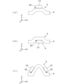
- FIG. 5 is a diagram showing some examples of shapes of the bent portion of the protruding portion 5.
- FIG. FIG. 5 is a diagram showing some examples of shapes of the bent portion of the protruding portion 5.
- FIG. 6 is a diagram illustrating a structure in which components are mounted using protrusions.
- FIG. 7 is a view of the laminated substrate 102 as viewed from the cutting position of the flat portion (the portion continuing from the bent portion) in the direction of the protruding portion 5.
- FIG. 8 is a view of the laminated substrate 102 cut at the center of the protruding portion 5, looking at the cut position and the flat portion (continuous portion of the bent portion) behind the cut position.
- FIG. 9 is a cross-sectional view showing the laminated structure of insulating layers and conductor layers of the laminated substrate 102. As shown in FIG. FIG. FIG.
- FIG. 10 is a view of the laminated substrate 103 as viewed from the cutting position of the flat portion (continuous portion of the bent portion) in the direction of the protruding portion 5.
- FIG. 11 is a view of the laminated substrate 103 cut at the center of the protruding portion 5, looking at the cut position and the flat portion (continuous portion of the bent portion) behind the cut position.
- FIG. 12 is a view of the laminated substrate 104 as viewed from the cut position of the flat portion (continuous portion of the bent portion) in the direction of the protruding portion 5.
- FIG. 13 is a view of the laminated substrate 104 cut at the center of the protruding portion 5, looking at the cut position and the flat portion (continuous portion of the bent portion) behind the cut position.
- FIG. 14 is a cross-sectional view taken along a direction passing through a protruding portion 5 of a laminate 4 of a laminated substrate 105 according to the fifth embodiment and along the longitudinal direction of a bent portion 1.
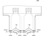
- FIG. 15 is a perspective view of a laminated substrate 106 according to this embodiment.
- FIG. 16 is a view of the laminated substrate 106 cut at the center of the protruding portions 5A and 5B, looking at the cut position and the flat portion (continuous portion of the bent portion) behind the cut position.
- FIG. 17 is a perspective view of a component-mounted laminated substrate 107A according to this embodiment, viewed from two directions.
- FIG. 18 is a diagram showing a cut surface of the center of a bent portion 1 of a laminate 4 of a laminated substrate 107. As shown in FIG.
- FIG. 1 is a perspective view of a main part of a laminated substrate according to a first embodiment of the present invention, in which (a) in Fig. 1 is a perspective view of a laminated substrate 101, and (b) in Fig. 1 is a perspective view of a main part of a component-mounted laminated substrate configured by mounting a component 11 on the laminated substrate 101.
- the laminated substrate 101 includes a laminate 4 formed by stacking layers of insulating material and conductive films. A detailed example of the structure of this laminate 4 will be shown later.
- the laminate 4 has a bent portion 1 and bent portion continuation portions 2 and 3 that are continuous with the bent portion 1.
- the reference name "bent portion continuation portion” refers to the portion that is connected to and extends from the bent portion 1.
- the bent portion continuation portions 2 and 3 are both flat-shaped portions.
- the laminate 4 has a protrusion 5 on a part of the bent portion 1 that protrudes toward the inside of the bend of the bent portion 1.
- This protrusion 5 can also be called a rib or bead.
- conductor layers 21 and 22 are provided on the inner layer of the laminate 4. Terminal electrodes 31, 32, 33, 34, 35, and 36 are exposed at the component mounting positions near the end of the flat bent portion continuous portion 3.
- the front of the laminated substrate 101 is cut away to show the main part of the laminated substrate 101.
- the part of the laminated substrate 101 where the conductor layers 21 and 22 are exposed, as shown in (a) in FIG. 1, is the cut part of the laminated substrate 101.
- a plurality of conductor layers are formed inside (inner layers) of the laminate 4, and the conductor layers 21 and 22 are electrically connected to the terminal electrodes 31 and 32, respectively, via these conductor layers.
- component 11 has six terminals on its bottom surface, including terminals 61, 62, and 63.
- Terminals 61, 62, and 63 are soldered to terminal electrodes 31, 32, and 33, respectively, of laminated substrate 101.
- the remaining three terminals are soldered to terminal electrodes 34, 35, and 36, respectively.
- Not all of terminal electrodes 31 to 36 are necessarily conductive to the conductor layers formed in laminate 4, and there are cases in which they are used only for mounting component 11 to laminated substrate 101.
- FIG. 2 is a diagram showing a cut surface of the center of the bent portion 1 of the laminate 4 of the multilayer board.
- the protruding portion 5 is a part of the bent portion 1 that protrudes inward of the bend of the bent portion 1, and a hollow portion 6 is formed on the side opposite the protruding direction of the protruding portion 5.
- the inside (inner layer) of the laminate 4 is provided with conductor layers 21, 22.
- the conductor layers 21, 22 are conductor layers for signal transmission that extend in a direction that passes beyond the bent portion 1.
- the conductor layers 21, 22 for signal transmission are arranged in positions that avoid the protruding portion 5.
- the conductor layers 21, 22 for signal transmission are formed so that the non-protruding positions of the laminate 4 serve as a path.
- Fig. 3 The upper part of Fig. 3 is a cross-sectional view of the bent portion 1 of the laminate 4 at the center along the width direction.
- the lower part of Fig. 3 is a cross-sectional view of the bent portion 1 of the laminate 4 at the center along the length direction.
- the width W shown at the top of Figure 3 is the maximum dimension of the width of the cavity 6 on the opposite side of the protruding direction of the protruding portion 5 (Z direction in Figure 3) along the extension direction of the valley of the laminate 4 formed by folding the laminate 4 (X direction in Figure 3).
- the height H shown at the top of Figure 3 is the protrusion height, which is the dimension that protrudes the most.
- the thickness T shown in the upper part of Figure 3 is the thickness dimension of the laminate 4 at the portion where the protrusion 5 of the laminate 4 is formed.
- the length L shown at the bottom of Figure 3 is the protrusion length, which is the maximum length among the lengths in the direction perpendicular to the direction of the protrusion height H and the direction of the protrusion width W.
- the bent portion 1 of the laminate 4 shown in Figure 3 is the portion between the boundary between the curved surface and the flat surface on the inside of the bend of the bent portion 1 of the laminate 4.
- the protrusion width W, protrusion height H, and protrusion length L are all greater than or equal to the thickness T of the laminate 4.
- any one of the protrusion width W, protrusion height H, or protrusion length L may be equal to or greater than the thickness T of the laminate 4. This results in a laminate substrate 101 or a component-attached laminate substrate 101A having improved mechanical properties such as the rigidity of the bent portion 1.
- Figure 4 is a perspective view showing an example of the size relationship between the bent portion 1 and the protruding portion 5 of the laminate 4.
- part of the protruding portion 5 protrudes from the boundaries B2, B3 between the bent portion 1 and the bent portion continuous portions 2, 3 toward the bent portion continuous portions 2, 3, respectively.
- the two circles in Figure 4 indicate the start points of the protrusion.
- This can also be said to be that the length L of the protruding portion 5 shown in Figure 4 is longer than the length of the bent portion 1 (the length between the bent portion continuous portion 2 and the bent portion continuous portion 3). This structure enhances the effect of improving the rigidity of the bent portion.
- a laminated substrate 101 having improved mechanical properties such as the rigidity of the bent portion 1 can be obtained. Furthermore, by mounting a component 11 on the laminated substrate 101, a laminated substrate 101A with a component having improved mechanical properties such as the rigidity of the bent portion 1 can be obtained.
- Figure 5 shows some examples of the shapes of the bent portion of the protrusion 5.
- the cut surface is shown in a plane passing through the center of the protrusion 5 (a plane along the extension direction (X direction) of the valley of the laminate 4 formed by bending the laminate 4).
- the protrusion 5 has a flat portion FP at its apex. In this way, the apex of the protrusion 5 does not have to be a curved surface.
- the protrusion 5 has an asymmetric shape in cross section.
- the shape of the protrusion 5 may be asymmetric in a plane perpendicular to the longitudinal direction of the protrusion 5. This allows the rigidity characteristics of the bending portion to be intentionally made asymmetric. Also, when conductor layers (not shown in FIG. 5) to be placed on the laminate 4 are placed according to their electrical characteristics, it becomes easier to place them asymmetrically.
- the protrusion 5 has a larger width W relative to its height H than the examples shown in FIG. 2, FIG. 3, etc.
- the height of the protrusion 5 is low, so when the bending angle at the bending portion 1 of the bending portion continuation portions 2, 3 (see FIG. 1) is small, the protrusion is small in volume, allowing space to be saved.
- the protrusion 5 has a width W and a height H that are approximately equal to each other, or the height H is greater than the width W, as compared to the examples shown in FIG. 2, FIG. 3, etc.
- This structure makes it easy to increase the rigidity of the bent portion. Also, as will be exemplified later, it is easy to increase the shielding and isolation between the conductor layers for signal transmission that are positioned to avoid the protrusion.
- the shape, width, and height of the protrusion 5 can be determined as appropriate.
- FIG. 6 is a diagram illustrating a structure in which components are mounted using a protrusion. Here, a cut surface is shown in a plane passing through the center of the protrusion 5 (a plane along the extension direction (X direction) of the valley of the laminate 4 formed by bending the laminate 4).
- the protrusion 5 has a flat portion FP on its outer surface, and the component 12 is mounted on this flat portion FP.
- the component 12 can be provided without using the surface of the bent portion continuation portion, such as the flat portion of the laminate 4.
- the electrical influence on the conductor layer arranged on the bent portion continuation portion, such as the flat portion of the laminate 4 can be suppressed.
- connection and coupling with a transmission line passing through the protrusion 5 can be easily performed.
- the protrusion 5 has a flat portion FP on its inner surface, and a component 13 is mounted on this flat portion FP.
- This structure provides the same effect as the example shown in FIG. 6(a).
- the component 13 is mounted in the hollow portion 6, the overall space can be used efficiently.
- the protrusion 5 has a flat portion FP on its outer surface.
- Components 14, 15 are mounted on this flat portion FP. With this structure, the same effect as the example shown in FIG. 6(a) can be obtained. In addition, because components 14, 15 are mounted within the height range of the protrusion 5, the overall space can be used efficiently.
- the component 11 of the component-equipped laminated board 101A shown in the first embodiment is, for example, a connector.
- the connector of this component-equipped laminated board 101A is connected to a connector on another circuit board.
- This component-equipped laminated board 101A can be used as a cable.
- one end of the laminate 4 is the mounting location for the component 11, and the other end is not shown, but this other end may also be the mounting location for the component. It may also be directly connected to another circuit board.
- a laminated substrate 102 in which a laminate 4 includes a conductor layer for signal transmission will be illustrated.
- FIG. 7 is a view of the laminated substrate 102, viewed from the cutting position of the flat portion (continuation of the bent portion) toward the protruding portion 5.
- FIG. 8 is a view of the laminated substrate 102, cut at the center of the protruding portion 5, viewed from the cutting position and the flat portion (continuation of the bent portion) behind it.
- the laminated substrate 102 according to the second embodiment includes a conductor layer for signal transmission that extends in a direction that passes through the bent portion in the laminate 4.
- conductor layers 21, 21G1, 21G2 and conductor layers 22, 22G1, 22G2 are formed in the laminate 4. All of these conductor layers extend in the directions of the bent portion continuous portion (flat portion) 2, the bent portion 1, and the bent portion continuous portion (flat portion) 3 shown in Fig. 1 in the first embodiment.
- the conductor layer 21 is a signal line layer, the conductor layer 21G1 is a lower ground wiring layer, and the conductor layer 21G2 is an upper ground wiring layer. These conductor layers 21, 21G1, and 21G2 form a first stripline.
- the conductor layer 22 is a signal line layer
- the conductor layer 22G1 is a lower ground wiring layer
- the conductor layer 22G2 is an upper ground wiring layer.
- an electrically insulating protective film 7 is formed on the top and bottom surfaces of the laminate 4.
- FIG. 8 shows the patterns between the conductor layers 21, 22 and the terminal electrodes 31, 32 that respectively constitute the signal line layers.
- the conductor layer 21 of the first strip line constituted by the conductor layers 21, 21G1, 21G2 is connected to the terminal electrode 31.
- the conductor layer 22 of the second strip line constituted by the conductor layers 22, 22G1, 22G2 is connected to the terminal electrode 32.
- a cavity 6 is formed on the opposite side of the protrusion 5.
- Figure 9 is a cross-sectional view showing the laminated structure of the insulating layers and conductor layers of the laminated substrate 102.
- the upper part of Figure 9 shows the insulating layers and conductor layers of each layer before the laminate is formed, and the lower part of Figure 9 shows the laminate 4 after it has been formed.
- the manufacturing process for the laminated substrate 102 is as follows:
- conductor layers 21G1 and 22G1 are formed as ground conductor layers on the lower surface of insulator layer 10.
- Conductor layers 21 and 22 for signal transmission are formed on the upper surface of insulator layer 42.
- Conductor layers 21G2 and 22G2 are formed as ground conductor layers on the upper surface of insulator layer 43.
- the material of insulator layers 41, 42, and 43 is, for example, LCP (liquid crystal polymer).
- Conductor layers 21G1, 21, 21G2, 22G1, 22, and 22G2 are, for example, Cu film or Al film. These conductor layers are formed by attaching them to the entire surface of the insulator layer and patterning them.
- this protective film 7 is, for example, PI (polyimide).
- the laminate 4 coated with the protective film 7 is heated while bending a predetermined portion with a jig to form the bent portion 1.
- the laminate 4 is bent with the jig and the protrusion 5 is formed at the same time.
- the protrusion 5 may be formed by punching from the outside of the bent portion.
- the protrusion 5 is formed at the same time as bending the laminate 4, abnormal deformation and deterioration of the insulating layer and the conductor layer can be suppressed.
- the mechanical rigidity of the bending portion 1 is high, the distance between the bending portion continuous portion 2 and the bending portion continuous portion 3, which are continuous with the bending portion 1, is stabilized.
- the extension and contraction of the conductor layer for signal transmission and its vibration are suppressed, and the fluctuation of the electrical resistance of the conductor layer is suppressed.
- the fluctuation of the electrical resistance value due to heat generated by friction between the insulator layer and the conductor layer is suppressed.
- electrical noise for the electrical signal to be transmitted is suppressed.
- conductor layer 21G1 and conductor layer 22G1 are formed from a continuous conductor layer, the isolation between the first stripline and the second stripline can be improved.
- a laminated substrate having a conductor layer for improving rigidity on a protruding portion will be described as an example.
- FIG. 10 is a view of the laminated substrate 103, viewed from the cut position of the flat portion (continuation of the bent portion) toward the protruding portion 5.
- FIG. 11 is a view of the laminated substrate 103, cut at the center of the protruding portion 5, viewed from the cut position and the flat portion (continuation of the bent portion) behind it.
- the conductor layer 21 is a signal line layer
- the conductor layer 21G1 is a lower ground wiring layer
- the conductor layer 21G2 is an upper ground wiring layer.
- the conductor layers 21, 21G1, and 21G2 form a first stripline.
- the conductor layer 22 is a signal line layer
- the conductor layer 22G1 is a lower ground wiring layer
- the conductor layer 22G2 is an upper ground wiring layer.
- the laminated substrate 103 according to the third embodiment has a conductor layer inside (inner layer) of the protruding portion 5 of the laminate 4.
- a conductor layer 23 is arranged not only inside (inner layer) of the protruding portion 5 but also between the two striplines. This conductor layer 23 may be used as a conductor for signal transmission separate from the first and second striplines.
- a laminated substrate 104 having a signal transmission conductor layer on a protruding portion 5 will be illustrated.
- FIG. 12 is a view of the laminated substrate 104, viewed from the cut position of the flat portion (continuation of the bent portion) toward the protruding portion 5.
- FIG. 13 is a view of the laminated substrate 104, cut at the center of the protruding portion 5, viewed from the cut position and the flat portion (continuation of the bent portion) behind it.
- the conductor layer 21 is a signal line layer
- the conductor layer 21G1 is a lower ground wiring layer
- the conductor layer 21G2 is an upper ground wiring layer.
- the conductor layers 21, 21G1, and 21G2 form a first stripline.
- the conductor layer 22 is a signal line layer
- the conductor layer 22G1 is a lower ground wiring layer
- the conductor layer 22G2 is an upper ground wiring layer.
- the conductor layer 23 is a signal line layer
- the conductor layer 23G1 is a lower ground wiring layer
- the conductor layer 23G2 is an upper ground wiring layer.
- These conductor layers 23, 23G1, and 23G2 form a third stripline. This third stripline passes through the protrusion 5.
- the signal transmission conductor layer is not provided to avoid the position of the protrusion 5, so the number of signal transmission lines per width in the direction perpendicular to the signal transmission direction can be increased.
- the overall line length of the signal transmission line passing through the protrusion 5 can be shortened, which reduces loss of the transmitted signal.
- a laminated substrate including a conductor layer having an interlayer connection conductor will be illustrated.
- FIG. 14 is a cross-sectional view of the laminate 4 of the laminated substrate 105 according to the fifth embodiment taken along the longitudinal direction of the bent portion 1 and passing through the protruding portion 5.
- the conductor layers 23A and 23B are connected to each other by a plurality of interlayer connection conductors 8.
- the conductor layer 23G1 is the lower ground wiring layer
- the conductor layer 23G2 is the upper ground wiring layer.
- the conductor layers 23A and 23B, the interlayer connection conductors 8, the conductor layer 23G1, and the conductor layer 23G2 form a stripline that passes through the inner layer of the protrusion 5.
- the conductor layer for signal transmission may be composed of multiple conductor layers and interlayer connection conductors that connect them between the layers.
- Figure 15 is a perspective view of the laminated substrate 106 according to this embodiment.
- Figure 16 is a view of the laminated substrate 106 cut at the center of the protruding portions 5A and 5B, looking at the cut position and the flat portion (the portion continuing from the bent portion) behind the cut position.
- the laminate 4 has a bent portion 1 and bent portion continuation portions 2 and 3 that are continuous with the bent portion 1.
- the bent portion continuation portions 2 and 3 are both flat shaped portions.
- the laminate 4 has protrusions 5A and 5B at two locations in the bent portion 1 that protrude toward the inside of the bend of the bent portion 1.
- the laminate 4 is formed with conductor layers 21, 21G1, 21G2, 22, 22G1, 22G2, 23, 23G1, 23G2, 24, 24G1, and 24G2.
- the laminate 4 is also formed with a component mounting portion PMD.
- the first stripline is formed by conductor layers 21, 21G1, and 21G2.
- the second stripline is formed by conductor layers 22, 22G1, and 22G2.
- the third stripline is formed by conductor layers 23, 23G1, and 23G2
- the fourth stripline is formed by conductor layers 24, 24G1, and 24G2.
- the bent portion 1 in order to form the bent portion 1, multiple protrusions 5A, 5B are formed in the extension direction (X direction) of the valley of the laminate formed by bending the laminate 4, so that a laminate substrate 106 having high rigidity of the bent portion 1 can be obtained even if the extension direction of the valley of the laminate is long.
- the degree of freedom in arranging the conductor layer as a transmission line is increased.
- a signal line conductor may be formed on the surface or inner layer of the protrusions 5A and 5B.
- each protrusion 5A, 5B may be provided in a variety of sizes (width, height, length) of different protrusions 5A, 5B.
- a laminated substrate having a conductor layer having an active function on the upper surface or inner layer of the protruding portion 5 will be exemplified.
- FIG. 17 is a perspective view of the component-attached laminated substrate 107A according to this embodiment, viewed from two directions.
- the upper view of FIG. 17 is a perspective view from a direction in which the protruding portion 5 of the laminated substrate of the component-attached laminated substrate 107A is visible
- the lower view of FIG. 17 is a perspective view from a direction in which the hollow portion 6 of the laminated substrate of the component-attached laminated substrate 107A is visible.
- FIG. 18 is a diagram showing a cut surface of the center of the bent portion 1 of the laminate 4 of the laminated substrate 107.
- the laminate 4 has a bent portion 1 and bent portion continuation portions 2 and 3 that are continuous with the bent portion 1.
- the laminate 4 has a protruding portion 5 in a part of the bent portion 1 that protrudes to the inside of the bend of the bent portion 1.
- a ground conductor G2A is formed on the top surface of the flat bent portion continuation part 2, and a ground conductor G2B is formed on the top surface of the flat bent portion continuation part 3.
- a ground conductor G2A is formed on the top surface of the bent portion continuous portion 2 of the laminate 4, and a ground conductor G2B is formed on the top surface of the bent portion continuous portion 3.
- a ground conductor G2C is formed on the bottom surfaces of the bent portion continuous portion 2, the bent portion 1, and the bent portion continuous portion 3.
- Signal transmission conductor layers 21 and 22 are formed on the inner layers.
- the first strip line is formed by the signal transmission conductor layer 21, the ground conductor G2C, and the ground conductor G2A.
- the second strip line is formed by the signal transmission conductor layer 22, the ground conductor G2C, and the ground conductor G2A.
- the signal transmission conductor layer 21 is an inner layer of the protrusion 5 and is extended to the top of the protrusion 5 via the extension conductor layer 21E.
- a radiating element 51 is formed on the upper surface of the protrusion 5. The power supply point of this radiating element 51 is connected to the extension conductor layer 21E via the interlayer electrode 21C and the interlayer connection conductor 8.
- the signal transmission conductor layer 22 is extended to the top of the protrusion 5 via an extension conductor layer in the inner layer of the protrusion 5.
- a radiating element 52 is formed on the upper surface of the protrusion 5.
- the extension conductor layer is connected to the power supply point of this radiating element 52 via an interlayer electrode and an interlayer connection conductor. In the cross-sectional position shown in Figure 18, the extension conductor layer, interlayer electrode, and interlayer connection conductor that are conductive to the radiating element 52 are not shown.
- the ground conductor G2C formed on the underside of the bend portion continuous portion 2, the bend portion 1, and the bend portion continuous portion 3 is formed widely in a position other than the cavity portion 6 (a position not facing the radiating elements 51, 52) as shown in the lower drawing in FIG. 17.
- This ground conductor G2C and the ground conductor G2A are electrically connected via an interlayer connection conductor.
- the ground conductor G2C and the ground conductor G2B are electrically connected via an interlayer connection conductor.
- These interlayer connection conductors are arranged at predetermined intervals between the signal transmission conductor layer 21 and the signal transmission conductor layer 22 and in the longitudinal direction of the bend portion (the continuous direction of the bend portion continuous portion 2, the bend portion 1, and the bend portion continuous portion 3).
- the radiating element 51 acts as a first patch antenna, and the antenna signal is input and output via the first strip line.
- the radiating element 52 acts as a second patch antenna, and the antenna signal is input and output via the second strip line.
- the radiating elements 51, 52, etc. can be formed so as to straddle the protrusion 5, so multiple radiating elements can be easily formed.
- the orientations of the radiating elements 51, 52 are different, so multiple antennas with different directivities can be constructed. Therefore, it can be used as an antenna with wide directivity.
- the lower diagram in Figure 17 shows an example in which a ground conductor is not formed on the inner surface of cavity 6, but a ground conductor surface facing radiating elements 51 and 52 may be formed by forming a ground conductor on the inner surface of cavity 6. This makes it possible to suppress the influence of fluctuations in antenna characteristics due to other conductors close to radiating elements 51 and 52, for example.
- the protrusion 5 has an asymmetrical shape in cross section, as in the example shown in FIG. 5(b), it is possible to make the antenna's directivity asymmetric.
- the radiating elements 51 and 52 of the same shape are arranged with 180 degree rotational symmetry, but it is also possible to arrange multiple radiating elements with different frequency characteristics, for example by different sizes. In this way, an antenna for use in multiple frequency bands can be configured.
- the radiating elements 51 and 52 are formed on the surface of the protrusion 5, but the radiating elements may be provided on the inner layer.
- the conductor layer formed on the protrusion 5 is not limited to a radiating element, but may be a functional conductor layer such as a capacitor or inductor.
- an electronic device in the eighth embodiment, includes a housing that houses various boards and components.
- a housing for example, a circuit board is housed, and the laminated board shown in each of the above embodiments is also arranged.
- an electronic device with high mechanical strength against vibration can be configured.
- an electronic device with high electrical stability against vibration and reduced noise generation can be configured.
- the bent portion continuation portion that is connected to and extends from the bent portion of the laminate has a flat shape, but it may be curved.
- the area other than the bent portion is flexible, making it easy to incorporate into the housing of an electronic device.
- components mounted on the laminated substrate may also be chip components such as microphones, ICs, chip capacitors, and chip inductors.
- the laminated substrate, cable, and electronic device of the present invention may be provided in the following forms:
- a part of the conductor layer formed on the surface of the protrusion or on the inner layer of the protrusion has a plurality of layers, and includes an interlayer connection conductor for conducting the plurality of conductor layers between the layers;
- the laminated substrate according to ⁇ 1> is a part of the conductor layer formed on the surface of the protrusion or on the inner layer of the protrusion.
- a portion of the conductor layer is a conductor layer for signal transmission extending in a direction passing through the bent portion.
- At least a part of the conductor layer for signal transmission is disposed at a position passing through the protrusion.
- At least a part of the conductor layer for signal transmission is disposed at a position that avoids the protruding portion.
- a protective film is formed on the surface of the laminate.
- a protrusion width which is a maximum dimension of a width of a hollow portion on the opposite side of a protruding direction of the protrusion along an extension direction of a valley of the laminate formed by folding the laminate
- a protrusion height which is a dimension of the protrusion that protrudes the highest among the protrusions
- a protrusion length which is a maximum length among lengths in a direction perpendicular to the protrusion height direction and the protrusion width direction, are each equal to or greater than a thickness of the laminate.
- ⁇ 9> a portion of the protruding portion protruding from a boundary between the bent portion and the bent portion continuous portion toward the bent portion continuous portion; ⁇ 9> The laminated substrate according to any one of ⁇ 1> to ⁇ 8>.
- the laminate includes a radiating element formed on a surface of the protrusion or at a position including a surface layer of the protrusion.
- the laminated substrate according to any one of ⁇ 1> to ⁇ 10>.
- the material of the insulator layer is a thermoplastic resin.
- a component is mounted on the bent portion continuous portion.
- the bent portion has a flat portion on a surface of the bent portion, and a component is mounted on the flat portion.
- the part is a connector.
- a cable comprising the laminated substrate according to ⁇ 13> or ⁇ 14>.
- An electronic device comprising a housing, in which the laminated substrate according to any one of ⁇ 1> to ⁇ 14> or the cable according to ⁇ 15> is disposed.
Landscapes
- Engineering & Computer Science (AREA)
- Microelectronics & Electronic Packaging (AREA)
- Manufacturing & Machinery (AREA)
- Physics & Mathematics (AREA)
- Electromagnetism (AREA)
- Structure Of Printed Boards (AREA)
Priority Applications (2)
| Application Number | Priority Date | Filing Date | Title |
|---|---|---|---|
| JP2025527486A JP7794364B2 (ja) | 2023-06-13 | 2024-04-04 | 積層基板、ケーブル及び電子機器 |
| US19/366,814 US20260052626A1 (en) | 2023-06-13 | 2025-10-23 | Multilayer substrate, cable, and electronic apparatus |
Applications Claiming Priority (2)
| Application Number | Priority Date | Filing Date | Title |
|---|---|---|---|
| JP2023-096857 | 2023-06-13 | ||
| JP2023096857 | 2023-06-13 |
Related Child Applications (1)
| Application Number | Title | Priority Date | Filing Date |
|---|---|---|---|
| US19/366,814 Continuation US20260052626A1 (en) | 2023-06-13 | 2025-10-23 | Multilayer substrate, cable, and electronic apparatus |
Publications (1)
| Publication Number | Publication Date |
|---|---|
| WO2024257449A1 true WO2024257449A1 (ja) | 2024-12-19 |
Family
ID=93851808
Family Applications (1)
| Application Number | Title | Priority Date | Filing Date |
|---|---|---|---|
| PCT/JP2024/013941 Ceased WO2024257449A1 (ja) | 2023-06-13 | 2024-04-04 | 積層基板、ケーブル及び電子機器 |
Country Status (3)
| Country | Link |
|---|---|
| US (1) | US20260052626A1 (https=) |
| JP (1) | JP7794364B2 (https=) |
| WO (1) | WO2024257449A1 (https=) |
Citations (6)
| Publication number | Priority date | Publication date | Assignee | Title |
|---|---|---|---|---|
| JPH0220736Y2 (https=) * | 1984-08-29 | 1990-06-06 | ||
| JP2001339125A (ja) * | 2000-05-30 | 2001-12-07 | Fujikura Ltd | フレキシブルプリント基板 |
| WO2014109135A1 (ja) * | 2013-01-08 | 2014-07-17 | 株式会社村田製作所 | フレキシブル基板および電子機器 |
| WO2015015959A1 (ja) * | 2013-08-02 | 2015-02-05 | 株式会社村田製作所 | 高周波信号伝送線路及び電子機器 |
| JP2017123421A (ja) * | 2016-01-08 | 2017-07-13 | 株式会社村田製作所 | 配線基板及び電子機器 |
| DE102019130078A1 (de) * | 2019-11-07 | 2021-05-12 | Auto-Kabel Management Gmbh | Kraftfahrzeugenergieleitung sowie ein Verfahren zum Biegen einer Kraftfahrzeugenergieleitung |
-
2024
- 2024-04-04 JP JP2025527486A patent/JP7794364B2/ja active Active
- 2024-04-04 WO PCT/JP2024/013941 patent/WO2024257449A1/ja not_active Ceased
-
2025
- 2025-10-23 US US19/366,814 patent/US20260052626A1/en active Pending
Patent Citations (6)
| Publication number | Priority date | Publication date | Assignee | Title |
|---|---|---|---|---|
| JPH0220736Y2 (https=) * | 1984-08-29 | 1990-06-06 | ||
| JP2001339125A (ja) * | 2000-05-30 | 2001-12-07 | Fujikura Ltd | フレキシブルプリント基板 |
| WO2014109135A1 (ja) * | 2013-01-08 | 2014-07-17 | 株式会社村田製作所 | フレキシブル基板および電子機器 |
| WO2015015959A1 (ja) * | 2013-08-02 | 2015-02-05 | 株式会社村田製作所 | 高周波信号伝送線路及び電子機器 |
| JP2017123421A (ja) * | 2016-01-08 | 2017-07-13 | 株式会社村田製作所 | 配線基板及び電子機器 |
| DE102019130078A1 (de) * | 2019-11-07 | 2021-05-12 | Auto-Kabel Management Gmbh | Kraftfahrzeugenergieleitung sowie ein Verfahren zum Biegen einer Kraftfahrzeugenergieleitung |
Also Published As
| Publication number | Publication date |
|---|---|
| JP7794364B2 (ja) | 2026-01-06 |
| JPWO2024257449A1 (https=) | 2024-12-19 |
| US20260052626A1 (en) | 2026-02-19 |
Similar Documents
| Publication | Publication Date | Title |
|---|---|---|
| JP5970719B2 (ja) | 回路基板 | |
| JP6048633B1 (ja) | 複合伝送線路および電子機器 | |
| US9692100B2 (en) | Multi-layer resin substrate having grounding conductors configured to form triplate line sections and microstrip sections | |
| JP5842850B2 (ja) | フラットケーブルおよび電子機器 | |
| US9705194B2 (en) | Antenna module | |
| WO2020130010A1 (ja) | 伝送線路部材 | |
| US10342125B2 (en) | Multilayer substrate | |
| US10403989B2 (en) | Resin multilayer substrate and electronic device | |
| WO2015141016A1 (ja) | アンテナ装置、無線通信端末 | |
| JP6197979B1 (ja) | 樹脂基板および電子機器 | |
| JP7060171B2 (ja) | 伝送線路及び回路基板 | |
| JP7001154B2 (ja) | 伝送線路及びその実装構造 | |
| JPWO2017094574A1 (ja) | フィルタ回路付き配線基板および電子機器 | |
| JP7435751B2 (ja) | 多層基板 | |
| JP7794364B2 (ja) | 積層基板、ケーブル及び電子機器 | |
| US12191553B2 (en) | Transmission line | |
| US11515069B2 (en) | Multilayer substrate and electronic device | |
| JP7283484B2 (ja) | 多層基板 | |
| CN217363377U (zh) | 传输线路以及电子设备 | |
| WO2017199824A1 (ja) | 多層基板、および、電子機器 | |
| US12609431B2 (en) | Transmission line and electronic device including the same | |
| WO2025253722A1 (ja) | アンテナ基板、アンテナ及び電子機器 | |
| JPWO2019017206A1 (ja) | 回路モジュール | |
| JP4333659B2 (ja) | フレキシブル配線基板 | |
| JP5673891B1 (ja) | アンテナ装置、無線通信端末 |
Legal Events
| Date | Code | Title | Description |
|---|---|---|---|
| 121 | Ep: the epo has been informed by wipo that ep was designated in this application |
Ref document number: 24823072 Country of ref document: EP Kind code of ref document: A1 |
|
| ENP | Entry into the national phase |
Ref document number: 2025527486 Country of ref document: JP Kind code of ref document: A |
|
| WWE | Wipo information: entry into national phase |
Ref document number: 2025527486 Country of ref document: JP |
|
| NENP | Non-entry into the national phase |
Ref country code: DE |