WO2024253050A1 - 垂直共振器型発光素子 - Google Patents
垂直共振器型発光素子 Download PDFInfo
- Publication number
- WO2024253050A1 WO2024253050A1 PCT/JP2024/020134 JP2024020134W WO2024253050A1 WO 2024253050 A1 WO2024253050 A1 WO 2024253050A1 JP 2024020134 W JP2024020134 W JP 2024020134W WO 2024253050 A1 WO2024253050 A1 WO 2024253050A1
- Authority
- WO
- WIPO (PCT)
- Prior art keywords
- semiconductor layer
- region
- layer
- metal oxide
- type semiconductor
- Prior art date
- Legal status (The legal status is an assumption and is not a legal conclusion. Google has not performed a legal analysis and makes no representation as to the accuracy of the status listed.)
- Ceased
Links
Images



Classifications
-
- H—ELECTRICITY
- H01—ELECTRIC ELEMENTS
- H01S—DEVICES USING THE PROCESS OF LIGHT AMPLIFICATION BY STIMULATED EMISSION OF RADIATION [LASER] TO AMPLIFY OR GENERATE LIGHT; DEVICES USING STIMULATED EMISSION OF ELECTROMAGNETIC RADIATION IN WAVE RANGES OTHER THAN OPTICAL
- H01S5/00—Semiconductor lasers
- H01S5/04—Processes or apparatus for excitation, e.g. pumping, e.g. by electron beams
- H01S5/042—Electrical excitation ; Circuits therefor
- H01S5/0425—Electrodes, e.g. characterised by the structure
- H01S5/04252—Electrodes, e.g. characterised by the structure characterised by the material
-
- H—ELECTRICITY
- H01—ELECTRIC ELEMENTS
- H01S—DEVICES USING THE PROCESS OF LIGHT AMPLIFICATION BY STIMULATED EMISSION OF RADIATION [LASER] TO AMPLIFY OR GENERATE LIGHT; DEVICES USING STIMULATED EMISSION OF ELECTROMAGNETIC RADIATION IN WAVE RANGES OTHER THAN OPTICAL
- H01S5/00—Semiconductor lasers
- H01S5/04—Processes or apparatus for excitation, e.g. pumping, e.g. by electron beams
- H01S5/042—Electrical excitation ; Circuits therefor
- H01S5/0425—Electrodes, e.g. characterised by the structure
- H01S5/04256—Electrodes, e.g. characterised by the structure characterised by the configuration
-
- H—ELECTRICITY
- H01—ELECTRIC ELEMENTS
- H01S—DEVICES USING THE PROCESS OF LIGHT AMPLIFICATION BY STIMULATED EMISSION OF RADIATION [LASER] TO AMPLIFY OR GENERATE LIGHT; DEVICES USING STIMULATED EMISSION OF ELECTROMAGNETIC RADIATION IN WAVE RANGES OTHER THAN OPTICAL
- H01S5/00—Semiconductor lasers
- H01S5/04—Processes or apparatus for excitation, e.g. pumping, e.g. by electron beams
- H01S5/042—Electrical excitation ; Circuits therefor
- H01S5/0425—Electrodes, e.g. characterised by the structure
- H01S5/04256—Electrodes, e.g. characterised by the structure characterised by the configuration
- H01S5/04257—Electrodes, e.g. characterised by the structure characterised by the configuration having positive and negative electrodes on the same side of the substrate
-
- H—ELECTRICITY
- H01—ELECTRIC ELEMENTS
- H01S—DEVICES USING THE PROCESS OF LIGHT AMPLIFICATION BY STIMULATED EMISSION OF RADIATION [LASER] TO AMPLIFY OR GENERATE LIGHT; DEVICES USING STIMULATED EMISSION OF ELECTROMAGNETIC RADIATION IN WAVE RANGES OTHER THAN OPTICAL
- H01S5/00—Semiconductor lasers
- H01S5/10—Construction or shape of the optical resonator, e.g. extended or external cavity, coupled cavities, bent-guide, varying width, thickness or composition of the active region
- H01S5/18—Surface-emitting [SE] lasers, e.g. having both horizontal and vertical cavities
- H01S5/183—Surface-emitting [SE] lasers, e.g. having both horizontal and vertical cavities having only vertical cavities, e.g. vertical cavity surface-emitting lasers [VCSEL]
- H01S5/18308—Surface-emitting [SE] lasers, e.g. having both horizontal and vertical cavities having only vertical cavities, e.g. vertical cavity surface-emitting lasers [VCSEL] having a special structure for lateral current or light confinement
-
- H—ELECTRICITY
- H01—ELECTRIC ELEMENTS
- H01S—DEVICES USING THE PROCESS OF LIGHT AMPLIFICATION BY STIMULATED EMISSION OF RADIATION [LASER] TO AMPLIFY OR GENERATE LIGHT; DEVICES USING STIMULATED EMISSION OF ELECTROMAGNETIC RADIATION IN WAVE RANGES OTHER THAN OPTICAL
- H01S5/00—Semiconductor lasers
- H01S5/10—Construction or shape of the optical resonator, e.g. extended or external cavity, coupled cavities, bent-guide, varying width, thickness or composition of the active region
- H01S5/18—Surface-emitting [SE] lasers, e.g. having both horizontal and vertical cavities
- H01S5/183—Surface-emitting [SE] lasers, e.g. having both horizontal and vertical cavities having only vertical cavities, e.g. vertical cavity surface-emitting lasers [VCSEL]
- H01S5/18341—Intra-cavity contacts
-
- H—ELECTRICITY
- H01—ELECTRIC ELEMENTS
- H01S—DEVICES USING THE PROCESS OF LIGHT AMPLIFICATION BY STIMULATED EMISSION OF RADIATION [LASER] TO AMPLIFY OR GENERATE LIGHT; DEVICES USING STIMULATED EMISSION OF ELECTROMAGNETIC RADIATION IN WAVE RANGES OTHER THAN OPTICAL
- H01S5/00—Semiconductor lasers
- H01S5/20—Structure or shape of the semiconductor body to guide the optical wave ; Confining structures perpendicular to the optical axis, e.g. index or gain guiding, stripe geometry, broad area lasers, gain tailoring, transverse or lateral reflectors, special cladding structures, MQW barrier reflection layers
- H01S5/2054—Methods of obtaining the confinement
- H01S5/2059—Methods of obtaining the confinement by means of particular conductivity zones, e.g. obtained by particle bombardment or diffusion
- H01S5/2063—Methods of obtaining the confinement by means of particular conductivity zones, e.g. obtained by particle bombardment or diffusion obtained by particle bombardment
-
- H—ELECTRICITY
- H01—ELECTRIC ELEMENTS
- H01S—DEVICES USING THE PROCESS OF LIGHT AMPLIFICATION BY STIMULATED EMISSION OF RADIATION [LASER] TO AMPLIFY OR GENERATE LIGHT; DEVICES USING STIMULATED EMISSION OF ELECTROMAGNETIC RADIATION IN WAVE RANGES OTHER THAN OPTICAL
- H01S5/00—Semiconductor lasers
- H01S5/04—Processes or apparatus for excitation, e.g. pumping, e.g. by electron beams
- H01S5/042—Electrical excitation ; Circuits therefor
- H01S5/0421—Electrical excitation ; Circuits therefor characterised by the semiconducting contacting layers
-
- H—ELECTRICITY
- H01—ELECTRIC ELEMENTS
- H01S—DEVICES USING THE PROCESS OF LIGHT AMPLIFICATION BY STIMULATED EMISSION OF RADIATION [LASER] TO AMPLIFY OR GENERATE LIGHT; DEVICES USING STIMULATED EMISSION OF ELECTROMAGNETIC RADIATION IN WAVE RANGES OTHER THAN OPTICAL
- H01S5/00—Semiconductor lasers
- H01S5/04—Processes or apparatus for excitation, e.g. pumping, e.g. by electron beams
- H01S5/042—Electrical excitation ; Circuits therefor
- H01S5/0425—Electrodes, e.g. characterised by the structure
- H01S5/04252—Electrodes, e.g. characterised by the structure characterised by the material
- H01S5/04253—Electrodes, e.g. characterised by the structure characterised by the material having specific optical properties, e.g. transparent electrodes
-
- H—ELECTRICITY
- H01—ELECTRIC ELEMENTS
- H01S—DEVICES USING THE PROCESS OF LIGHT AMPLIFICATION BY STIMULATED EMISSION OF RADIATION [LASER] TO AMPLIFY OR GENERATE LIGHT; DEVICES USING STIMULATED EMISSION OF ELECTROMAGNETIC RADIATION IN WAVE RANGES OTHER THAN OPTICAL
- H01S5/00—Semiconductor lasers
- H01S5/04—Processes or apparatus for excitation, e.g. pumping, e.g. by electron beams
- H01S5/042—Electrical excitation ; Circuits therefor
- H01S5/0425—Electrodes, e.g. characterised by the structure
- H01S5/04254—Electrodes, e.g. characterised by the structure characterised by the shape
-
- H—ELECTRICITY
- H01—ELECTRIC ELEMENTS
- H01S—DEVICES USING THE PROCESS OF LIGHT AMPLIFICATION BY STIMULATED EMISSION OF RADIATION [LASER] TO AMPLIFY OR GENERATE LIGHT; DEVICES USING STIMULATED EMISSION OF ELECTROMAGNETIC RADIATION IN WAVE RANGES OTHER THAN OPTICAL
- H01S5/00—Semiconductor lasers
- H01S5/10—Construction or shape of the optical resonator, e.g. extended or external cavity, coupled cavities, bent-guide, varying width, thickness or composition of the active region
- H01S5/18—Surface-emitting [SE] lasers, e.g. having both horizontal and vertical cavities
- H01S5/183—Surface-emitting [SE] lasers, e.g. having both horizontal and vertical cavities having only vertical cavities, e.g. vertical cavity surface-emitting lasers [VCSEL]
- H01S5/18305—Surface-emitting [SE] lasers, e.g. having both horizontal and vertical cavities having only vertical cavities, e.g. vertical cavity surface-emitting lasers [VCSEL] with emission through the substrate, i.e. bottom emission
-
- H—ELECTRICITY
- H01—ELECTRIC ELEMENTS
- H01S—DEVICES USING THE PROCESS OF LIGHT AMPLIFICATION BY STIMULATED EMISSION OF RADIATION [LASER] TO AMPLIFY OR GENERATE LIGHT; DEVICES USING STIMULATED EMISSION OF ELECTROMAGNETIC RADIATION IN WAVE RANGES OTHER THAN OPTICAL
- H01S5/00—Semiconductor lasers
- H01S5/10—Construction or shape of the optical resonator, e.g. extended or external cavity, coupled cavities, bent-guide, varying width, thickness or composition of the active region
- H01S5/18—Surface-emitting [SE] lasers, e.g. having both horizontal and vertical cavities
- H01S5/183—Surface-emitting [SE] lasers, e.g. having both horizontal and vertical cavities having only vertical cavities, e.g. vertical cavity surface-emitting lasers [VCSEL]
- H01S5/18344—Surface-emitting [SE] lasers, e.g. having both horizontal and vertical cavities having only vertical cavities, e.g. vertical cavity surface-emitting lasers [VCSEL] characterized by the mesa, e.g. dimensions or shape of the mesa
- H01S5/18347—Mesa comprising active layer
-
- H—ELECTRICITY
- H01—ELECTRIC ELEMENTS
- H01S—DEVICES USING THE PROCESS OF LIGHT AMPLIFICATION BY STIMULATED EMISSION OF RADIATION [LASER] TO AMPLIFY OR GENERATE LIGHT; DEVICES USING STIMULATED EMISSION OF ELECTROMAGNETIC RADIATION IN WAVE RANGES OTHER THAN OPTICAL
- H01S5/00—Semiconductor lasers
- H01S5/10—Construction or shape of the optical resonator, e.g. extended or external cavity, coupled cavities, bent-guide, varying width, thickness or composition of the active region
- H01S5/18—Surface-emitting [SE] lasers, e.g. having both horizontal and vertical cavities
- H01S5/183—Surface-emitting [SE] lasers, e.g. having both horizontal and vertical cavities having only vertical cavities, e.g. vertical cavity surface-emitting lasers [VCSEL]
- H01S5/18361—Structure of the reflectors, e.g. hybrid mirrors
- H01S5/18369—Structure of the reflectors, e.g. hybrid mirrors based on dielectric materials
-
- H—ELECTRICITY
- H01—ELECTRIC ELEMENTS
- H01S—DEVICES USING THE PROCESS OF LIGHT AMPLIFICATION BY STIMULATED EMISSION OF RADIATION [LASER] TO AMPLIFY OR GENERATE LIGHT; DEVICES USING STIMULATED EMISSION OF ELECTROMAGNETIC RADIATION IN WAVE RANGES OTHER THAN OPTICAL
- H01S5/00—Semiconductor lasers
- H01S5/20—Structure or shape of the semiconductor body to guide the optical wave ; Confining structures perpendicular to the optical axis, e.g. index or gain guiding, stripe geometry, broad area lasers, gain tailoring, transverse or lateral reflectors, special cladding structures, MQW barrier reflection layers
- H01S5/2054—Methods of obtaining the confinement
- H01S5/2059—Methods of obtaining the confinement by means of particular conductivity zones, e.g. obtained by particle bombardment or diffusion
- H01S5/2068—Methods of obtaining the confinement by means of particular conductivity zones, e.g. obtained by particle bombardment or diffusion obtained by radiation treatment or annealing
-
- H—ELECTRICITY
- H01—ELECTRIC ELEMENTS
- H01S—DEVICES USING THE PROCESS OF LIGHT AMPLIFICATION BY STIMULATED EMISSION OF RADIATION [LASER] TO AMPLIFY OR GENERATE LIGHT; DEVICES USING STIMULATED EMISSION OF ELECTROMAGNETIC RADIATION IN WAVE RANGES OTHER THAN OPTICAL
- H01S5/00—Semiconductor lasers
- H01S5/30—Structure or shape of the active region; Materials used for the active region
- H01S5/305—Structure or shape of the active region; Materials used for the active region characterised by the doping materials used in the laser structure
- H01S5/3054—Structure or shape of the active region; Materials used for the active region characterised by the doping materials used in the laser structure p-doping
- H01S5/3063—Structure or shape of the active region; Materials used for the active region characterised by the doping materials used in the laser structure p-doping using Mg
-
- H—ELECTRICITY
- H01—ELECTRIC ELEMENTS
- H01S—DEVICES USING THE PROCESS OF LIGHT AMPLIFICATION BY STIMULATED EMISSION OF RADIATION [LASER] TO AMPLIFY OR GENERATE LIGHT; DEVICES USING STIMULATED EMISSION OF ELECTROMAGNETIC RADIATION IN WAVE RANGES OTHER THAN OPTICAL
- H01S5/00—Semiconductor lasers
- H01S5/30—Structure or shape of the active region; Materials used for the active region
- H01S5/32—Structure or shape of the active region; Materials used for the active region comprising PN junctions, e.g. hetero- or double- heterostructures
- H01S5/323—Structure or shape of the active region; Materials used for the active region comprising PN junctions, e.g. hetero- or double- heterostructures in AIIIBV compounds, e.g. AlGaAs-laser, InP-based laser
- H01S5/32308—Structure or shape of the active region; Materials used for the active region comprising PN junctions, e.g. hetero- or double- heterostructures in AIIIBV compounds, e.g. AlGaAs-laser, InP-based laser emitting light at a wavelength less than 900 nm
- H01S5/32341—Structure or shape of the active region; Materials used for the active region comprising PN junctions, e.g. hetero- or double- heterostructures in AIIIBV compounds, e.g. AlGaAs-laser, InP-based laser emitting light at a wavelength less than 900 nm blue laser based on GaN or GaP
Definitions
- the present invention relates to a vertical cavity light emitting device.
- Patent Document 1 discloses a vertical cavity surface emitting laser (VCSEL) that includes a semiconductor structure layer that includes an n-type semiconductor layer, a light emitting layer, and a p-type semiconductor layer, with a protrusion formed on the upper surface of the p-type semiconductor layer, an insulating layer formed on the upper surface of the p-type semiconductor layer, and a light-transmitting electrode layer that includes the insulating layer and is formed on the upper surface of the p-type semiconductor layer.
- VCSEL vertical cavity surface emitting laser
- the threshold current increases with long-term current flow, and the output of the emitted light can decrease.
- hydrogen is injected into the p-type semiconductor layer to suppress the increase in threshold current, but depending on the hydrogen concentration in the p-type semiconductor layer, the flow of current may be suppressed too much, resulting in a problem of a smaller light-emitting area of the vertical cavity surface emitting laser.
- the present invention was made in consideration of the above points, and aims to provide a vertical cavity light emitting device that can prevent a decrease in light output while preventing a decrease in the light emitting area.
- the vertical cavity light emitting device is characterized by having a substrate, a first multilayer film reflector formed on the substrate, a semiconductor structure layer including a first semiconductor layer having a first conductivity type formed on the first multilayer film reflector, a light emitting layer formed on the first semiconductor layer, and a second semiconductor layer formed on the light emitting layer and having a second conductivity type opposite to the first conductivity type, a light-transmitting metal oxide film formed on the second semiconductor layer, covering one region in the center of the upper surface of the second semiconductor layer and electrically connected to the second semiconductor layer in the one region, partially formed on a peripheral region on the periphery of the one region and insulated from the surface of the second semiconductor layer in the peripheral region, and a second multilayer film reflector formed on the semiconductor structure layer so as to cover the one region and forming a resonator between itself and the first multilayer film reflector.
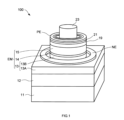
- FIG. 1 is a perspective view of a vertical cavity surface emitting laser according to a first embodiment
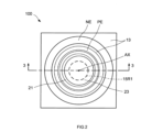
- FIG. 2 is a top view of the vertical cavity surface emitting laser according to the first embodiment
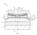
- 1 is a cross-sectional view of a vertical cavity surface emitting laser according to a first embodiment.
- FIG. 1 is a cross-sectional view of a conventional vertical-cavity surface-emitting laser.
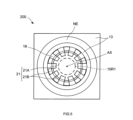
- FIG. 4 is a top view of a vertical cavity surface emitting laser according to a modified example of the first embodiment.
- FIG. 4 is a top view of a vertical cavity surface emitting laser according to a modified example of the first embodiment.
- FIG. 4 is a top view of a vertical cavity surface emitting laser according to a modified example of the first embodiment.
- FIG. 11 is a cross-sectional view of a vertical cavity surface emitting laser according to a second embodiment.
- FIG. 1 is a perspective view of the surface emitting laser 100.
- Figure 2 is a top view of the surface emitting laser 100, and
- Figure 3 is a cross-sectional view of the surface emitting laser 100 taken along line 3-3 shown in Figure 2. Note that in Figure 3, the up-down direction in the figure corresponds to the height direction of the surface emitting laser 100.
- the substrate 11 is a flat, transparent substrate with a rectangular top surface.
- the substrate 11 is a growth substrate on whose top surface a semiconductor crystal can be grown.
- the substrate 11 is made of a material that is translucent to light having a blue wavelength, such as undoped gallium nitride (GaN).
- GaN undoped gallium nitride
- the axis that passes through the center of the top surface of the substrate 11 and is perpendicular to the top surface is referred to as the central axis AX.
- the first multilayer reflector 12 is a semiconductor multilayer reflector made of semiconductor layers grown on the substrate 11.
- the first multilayer reflector 12 is a so-called distributed Bragg reflector (DBR) in which a high-refractive index semiconductor film with a relatively high refractive index and a low-refractive index semiconductor film with a lower refractive index than the high-refractive index semiconductor film are alternately stacked on the upper surface of the substrate 11.
- DBR distributed Bragg reflector
- the first multilayer reflector 12 is formed, for example, by stacking 42 pairs of a high refractive index semiconductor film made of GaN and a low refractive index semiconductor film made of aluminum indium nitride (AlInN) on the upper surface of the substrate 11.
- the first multilayer reflector 12 has such a configuration and is reflective to light in the blue wavelength range.
- a buffer layer (not shown) made of GaN is provided between the substrate 11 and the first multilayer reflector 12.
- the semiconductor structure layer EM is a laminated structure consisting of multiple semiconductor layers formed on the first multilayer reflector 12.
- the semiconductor structure layer EM has an n-type semiconductor layer 13 formed on the first multilayer reflector 12, a light-emitting layer 14 formed on the n-type semiconductor layer 13, and a p-type semiconductor layer 15 formed on the light-emitting layer 14.
- n-type semiconductor layer 13 The structures of the n-type semiconductor layer 13, the light-emitting layer 14, and the p-type semiconductor layer 15 that make up the semiconductor structure layer EM are described below.
- the n-type semiconductor layer 13 which is a first semiconductor layer having a first conductivity type, is a semiconductor layer formed over the upper surface of the first multilayer reflector 12.
- the n-type semiconductor layer 13 is made of GaN and is doped with silicon (Si) as an n-type impurity.
- the n-type semiconductor layer 13 has a so-called mesa-shaped structure consisting of a flat lower portion 13A and a cylindrical upper portion 13B that protrudes upward from the center of the lower portion 13A along the central axis AX (see Figures 1 and 3).
- the light-emitting layer 14 is formed over the upper portion 13B of the n-type semiconductor layer 13, and is a semiconductor layer having a quantum well structure in which a well layer made of InGaN and a barrier layer made of GaN are stacked on top of each other.
- the light-emitting layer 14 is formed so that its light-emitting center is brought onto the central axis AX.
- the light-emitting layer 14 emits blue light with a peak wavelength of, for example, 450 nm.
- the p-type semiconductor layer 15 which is a second semiconductor layer having a second conductivity type, is a semiconductor layer formed over the upper surface of the light-emitting layer 14.
- the p-type semiconductor layer 15 is made of GaN and is doped with magnesium (Mg) as a p-type impurity.
- the p-type semiconductor layer 15 has, on its upper surface, a first region 15R1 that has a circular shape and passes through the central axis AX, and a second region 15R2 that is an annular region on the periphery of the first region 15R1 and is recessed below the first region 15R1 (see FIG. 3).
- the p-type semiconductor layer 15 has a protrusion that protrudes upward in the center of the upper surface.
- the p-type semiconductor layer 15 also has a third region 15R3 on the upper surface, which is a peripheral region of the second region 15R2 and protrudes above the second region 15R2. That is, the p-type semiconductor layer 15 has a recess on the upper surface, the bottom of which is the second region 15R2.
- the second region 15R2 is a region in which the p-type impurity (Mg) doped into the p-type semiconductor layer 15 is electrically inactivated.
- the second region 15R2 is formed, for example, by performing dry etching on the top surface of the flat p-type semiconductor layer so as to leave regions corresponding to the first region 15R1 and the third region 15R3.
- the p-type impurities are inactivated by being damaged by dry etching. Specifically, the p-type impurities are placed in the lattice positions of the crystals of the p-type semiconductor layer 15 during the formation of the p-type semiconductor layer, and are thus in an electrically activated state.
- the p-type impurities are displaced from the lattice positions of the crystals of the p-type semiconductor layer 15 through dry etching, and are no longer able to function as acceptor ions due to defects created by dry etching, i.e., they are in an electrically inactive state.
- the second region 15R2 is a region in which the p-type impurities have difficulty generating carriers.
- the second region 15R2 functions as a high-resistance region having a higher electrical resistance than the first region 15R1.
- the hydrogen concentration is higher in the second portion 15P2, which is the peripheral portion of the first portion 15P1 and is also the portion along the second region 15R2 and the third region 15R3, than in the first portion 15P1, which is the portion along the first region 15R1 of the p-type semiconductor layer 15.
- the hydrogen concentration in the second portion 15P2 is at least twice as high as the hydrogen concentration in the first portion 15P1 in the p-type semiconductor layer 15.
- the hydrogen concentration in the first portion 15P1 is 1 ⁇ 10 18 /cm 3
- the hydrogen concentration in the second portion 15P2 is 2 ⁇ 10 18 /cm 3 .
- the insulating layer 19 is a transparent coating layer having electrical insulation properties that is formed continuously covering the second region 15R2 and the third region 15R3 on the upper surface of the p-type semiconductor layer 15. In other words, the insulating layer 19 is formed on the upper surface of the p-type semiconductor layer 15 so as to expose only the first region 15R1 of the upper surface of the p-type semiconductor layer 15.
- the insulating layer 19 is formed to have an inclined surface that slopes downward from the third region 15R3 to the second region 15R2 on the upper surface of the p-type semiconductor layer 15.
- the insulating layer 19 is made of a material having a lower refractive index than the p-type semiconductor layer 15, such as silicon dioxide (SiO 2 ).
- the conductive film 21 is a transparent metal oxide film that is formed to cover the first region 15R1 and extend from the first region 15R1 to partway through the second region 15R2 in a plan view of the p-type semiconductor layer 15 from above. In other words, the conductive film 21 is formed in such a manner that it covers the first region 15R1 but does not reach the outer edge of the upper surface of the p-type semiconductor layer 15.
- the conductive film 21 is electrically connected to the p-type semiconductor layer 15 in the first region 15R1, and is electrically insulated from the second region 15R2 and the third region 15R3 by the insulating layer 19. In other words, when a current flows through the conductive film 21, most of the current flows into the p-type semiconductor layer 15 via the first region 15R1.
- the conductive film 21 is made of a metal oxide, such as indium tin oxide (ITO) or indium zinc oxide (IZO), that is transparent to the blue light emitted from the light-emitting layer 14.
- ITO indium tin oxide
- IZO indium zinc oxide
- the thickness of the conductive film 21 depends on the absorptivity of the light emitted from the light-emitting layer 14, but is preferably 10 nm to 100 nm, and more preferably 10 nm to 50 nm.
- the conductive film 21 is formed, for example, by forming a metal oxide film made of ITO over the upper surface of the p-type semiconductor layer 15, and then removing the metal oxide film from the outer edge of the third region 15R3 to halfway through the second region by etching or plasma cleaning.
- the p-electrode PE is formed on the insulating layer 19 so as to cover the outer edge of the conductive film 21 along the outer edge of the upper surface of the p-type semiconductor layer 15, and is a metal electrode with a ring-shaped upper surface that is electrically connected to the conductive film 21.
- the p-electrode PE is formed, for example, from nickel (Ni) and gold (Au) in this order.
- the n-electrode NE is provided on the upper surface of the lower portion 13A of the n-type semiconductor layer 13, and is a metal electrode with a ring-shaped upper surface shape that is electrically connected to the n-type semiconductor layer 13.
- the n-electrode NE is formed so as to surround the upper portion 13B of the n-type semiconductor layer 13 while being spaced apart from the upper portion 13B.
- the n-electrode NE is formed, for example, by stacking titanium (Ti) and aluminum (Al) in this order on the upper surface of the lower portion 13A.
- the second multilayer reflector 23 is a cylindrical dielectric multilayer reflector made of a dielectric layer deposited on the upper surface of the conductive film 21. In a plan view of the surface-emitting laser 100 seen from above, the second multilayer reflector 23 is formed to cover the first region 15R1 while being spaced apart from the p-electrode PE.
- the second multilayer film reflector 23 is a so-called distributed Bragg reflector (DBR) in which a high refractive index dielectric film with a relatively high refractive index and a low refractive index dielectric film with a lower refractive index than the high refractive index dielectric film are alternately stacked on the upper surface of the conductive film 21.
- DBR distributed Bragg reflector
- the second multilayer film reflector 23 is formed, for example, by laminating 10.5 pairs of a high refractive index dielectric film made of niobium pentoxide (Nb 2 O 5 ) and a low refractive index dielectric film made of SiO 2 on the upper surface of the conductive film 21. By having such a configuration, the second multilayer film reflector 23 has reflectivity for the blue light emitted from the light emitting layer 14.
- a transparent dielectric layer (not shown) having a circular upper surface is formed between the second multilayer reflector 23 and the conductive film 21.
- the dielectric layer is made of, for example, Nb2O5 , tantalum pentoxide ( Ta2O5 ) , zinc oxide (ZrO2), titanium oxide ( TiO2 ), hafnium oxide ( HfO2 ) , or the like.
- the bottom surface of the second multilayer film reflector 23 faces the top surface of the first multilayer film reflector 12, sandwiching the dielectric layer, conductive film 21, and semiconductor structure layer EM.
- the first multilayer film reflector 12 and the second multilayer film reflector 23 form a resonator OC between the first multilayer film reflector 12 and the second multilayer film reflector 23, with the resonator length direction being perpendicular to the semiconductor structure layer EM (perpendicular to the substrate 11).
- the reflectance of the first multilayer reflector 12 for blue light is slightly lower than the reflectance of the second multilayer reflector 23 for blue light. Therefore, part of the blue light resonating in the resonator OC passes through the first multilayer reflector 12 and the substrate 11 and is extracted to the outside. In other words, the light resonating between the first multilayer reflector 12 and the second multilayer reflector 23 is emitted downward in FIG. 3.
- An anti-reflection film (not shown) made of a laminate of Nb 2 O 5 and SiO 2 is formed on the lower surface of the substrate 11.
- the anti-reflection film is a so-called AR coat that suppresses the blue light emitted from the substrate 11 from being reflected upward in FIG. 3 by the interface between the substrate 11 and the outside.
- the blue light emitted from the light-emitting layer 14 when the threshold current is reached is repeatedly reflected between the first multilayer reflector 12 and the second multilayer reflector 23, i.e., in the resonator OC, and reaches a resonant state (i.e., laser oscillation occurs).
- the central protruding portion of the p-type semiconductor layer 15 formed by the first region 15R1 and the second region 15R2 and the insulating layer 19 formed on the second region 15R2 function as a current confinement portion that limits the current supply range so that the current does not spread any further.
- the equivalent refractive index which is the average refractive index in the thickness direction between the first multilayer reflector 12 and the second multilayer reflector 23, is different between the cylindrical central region CA including the first region 15R1 of the p-type semiconductor layer 15 and the cylindrical peripheral region PA therearound.
- the refractive index of the insulating layer 19 in the peripheral region PA is lower than the refractive index of the protruding portion (p-type semiconductor layer 15) in the central region CA, so the equivalent refractive index in the central region CA is higher than the equivalent refractive index in the peripheral region PA.
- the surface-emitting laser 100 configured in this way, the optical loss caused by the standing waves in the central area CA diverging (radiating) to the peripheral area PA is suppressed. In other words, most of the light remains in the central area CA, and the laser light is extracted to the outside in this state.
- FIG. 4 is a cross-sectional view of a surface-emitting laser 110 as a conventional example.
- the surface-emitting laser 110 differs from the surface-emitting laser 100 in that the conductive film 21 is formed across the upper surface of the p-type semiconductor layer 15, but is the same in other respects.
- the hydrogen concentration in the second portion 15P2 of the p-type semiconductor layer 15 is higher than the hydrogen concentration in the first portion 15P1.
- an example of a method for creating a hydrogen concentration difference between the first portion 15P1 and the second portion 15P2 of the p-type semiconductor layer 15 during the fabrication of the surface-emitting laser 100 will be described.
- the conductive film 21 is formed gradually while containing hydrogen from the atmosphere by, for example, forming the conductive film 21 on the p-type semiconductor layer 15 by sputtering at a film formation rate of 2 nm/min at a temperature of 25° C.
- the hydrogen concentration in the conductive film 21 becomes, for example, about 1 ⁇ 10 21 /cm 3 .
- an electrode annealing process (600°C, 5 minutes) is performed to reduce the contact resistance between the conductive film 21 and the surface of the p-type semiconductor layer 15, so that the hydrogen contained in the conductive film 21 migrates into the p-type semiconductor layer 15 so that it remains at approximately the same concentration in the first portion 15P1 and the second portion 15P2 of the p-type semiconductor layer 15.
- a current is passed between the n-electrode NE and the p-electrode PE.
- the insulating layer 19 is formed in the second region 15R2 and the third region 15R3, most of the current flowing from the p-electrode PE to the n-electrode NE via the conductive film 21 flows via the first portion 15P1, and almost none flows through the second portion 15P2.
- the hydrogen remaining in the first portion 15P1 escapes into the n-type semiconductor layer 13 when electricity is applied, whereas most of the hydrogen remaining in the second portion 15P2 does not escape even when electricity is applied, and so remains in the second portion 15P2. Therefore, the hydrogen concentration in the second portion 15P2 is higher than the hydrogen concentration in the first portion 15P1.
- hydrogen in the p-type semiconductor layer 15 diffuses from the high concentration region to the low concentration region according to the concentration gradient, i.e., from the second portion 15P2 toward the first portion 15P1.
- the current that mostly flowed only through the first portion 15P1 when the surface-emitting laser 100 starts to operate may flow through the first portion 15P1 as well as through the second portion 15P2.
- a phenomenon may occur in which the current path of the current flowing through the p-type semiconductor layer 15 widens due to the long period of energization. If such a phenomenon occurs, the optical loss in the resonator OC increases, and the threshold current required for laser oscillation may increase.
- the diffusion force of hydrogen diffusing from the second portion 15P2 toward the first portion 15P1 can suppress the phenomenon of the current path widening within the p-type semiconductor layer 15 described above.
- the surface-emitting laser 100 is used for a long period of time in devices such as displays and headlamps that are used under constant current driving conditions, it is possible to prevent a decrease in the intensity of the emitted light due to an increase in the threshold current.
- the hydrogen concentration in the second portion 15P2 may be five or more times the hydrogen concentration in the first portion 15P1.
- the hydrogen in the second portion 15P2 will diffuse excessively into the first portion 15P1, and the diameter of the current passing through the first portion 15P1 (thick wavy line in Figure 4) will be narrower than the diameter of the first region 15R1.
- the diameter of the current flowing through the first portion 15P1 narrows, the diameter of the current injected into the light-emitting layer 14 also narrows, which can result in a phenomenon in which the area of the light emitted from the surface-emitting laser 110, i.e., the light-emitting area, becomes smaller.
- the conductive film 21 is formed in such a manner that it does not reach the outer edge of the upper surface of the p-type semiconductor layer 15.
- the volume of the conductive film 21 on the second portion 15P2 in the surface-emitting laser 100 of this embodiment is smaller than the volume of the conductive film 21 on the second portion 15P2 in the surface-emitting laser 110 of the conventional example.
- the surface-emitting laser 100 of this embodiment when electrode annealing of the conductive film 21 is performed during the fabrication of the surface-emitting laser 100 as described above, only the hydrogen contained in the conductive film 21 formed on the second portion 15P2 flows into the second portion 15P2. Therefore, the average hydrogen concentration in the second portion 15P2 in the surface-emitting laser 100 is smaller than the average hydrogen concentration in the second portion 15P2 in the surface-emitting laser 110.
- the hydrogen concentration in the second portion 15P2 can be reduced, thereby controlling the hydrogen concentration between the first portion 15P1 and the second portion 15P2 so that it does not become too high.
- the hydrogen concentration in the second portion 15P2 is at least twice the hydrogen concentration in the first portion 15P1.
- the hydrogen concentration in the second portion 15P2 is less than five times the hydrogen concentration in the first portion 15P1. Therefore, it is preferable that the hydrogen concentration in the second portion 15P2 is at least two times and less than five times the hydrogen concentration in the first portion 15P1.
- the surface-emitting laser 100 of this embodiment by forming the conductive film 21 so that it does not reach the outer edge of the upper surface of the p-type semiconductor layer 15, it is possible to prevent a decrease in the light output while preventing a decrease in the light-emitting area.
- Fig. 5 is a top view of a surface-emitting laser 200 according to the first modified example.
- the surface-emitting laser 200 is similar to the first embodiment in other respects, except for the formation of the conductive film 21, which is different from that in the first embodiment.
- the p-electrode PE and the second multilayer film reflector 23 are omitted to avoid complication of the drawing.
- the conductive film 21 is composed of a central portion 21A formed to cover the first region 15R1 on the upper surface of the p-type semiconductor layer 15, and extension portions 21B extending radially from the central portion 21A and reaching the outer edge of the third region 15R3. That is, in the surface-emitting laser 200 of this modified example, the conductive film 21 is formed so that the insulating layer 19 is exposed between adjacent extension portions 21B.
- the volume of the conductive film 21 formed on the second portion 15P2 is smaller than when the conductive film 21 is formed across the upper surface of the p-type semiconductor layer 15. Therefore, when fabricating the surface-emitting laser 200, it is possible to control the hydrogen concentration between the first portion 15P1 and the second portion 15P2 so that it does not become too high.
- the surface-emitting laser 200 of this modified example by partially forming the conductive film 21 on the second portion 15P2 of the p-type semiconductor layer 15, it is possible to prevent a decrease in the light output while preventing a decrease in the light-emitting area.
- the conductive film 21 is formed to have an inclined surface that follows the inclined surface of the insulating layer 19 described above.
- Fig. 6 is a top view of a surface-emitting laser 300 according to the second modification.
- the surface-emitting laser 300 differs from the first embodiment in the manner in which the conductive film 21 is formed, but is otherwise similar to the first embodiment. Note that, in Fig. 6 as well, the p-electrode PE and the second multilayer film reflector 23 are omitted to avoid complicating the drawing.
- the conductive film 21 is composed of a first conductive film 25 as a first metal oxide film formed to cover the first region 15R1 on the upper surface of the p-type semiconductor layer 15, and a second conductive film 26 as a second metal oxide film formed on the second region 15R2 and spaced apart from the first conductive film 25, as shown in FIG. 6.
- the volume of the conductive film 21 formed on the second portion 15P2 is smaller than when the conductive film 21 is formed across the upper surface of the p-type semiconductor layer 15. Therefore, when fabricating the surface-emitting laser 300, it is possible to control the hydrogen concentration between the first portion 15P1 and the second portion 15P2 so that it does not become too high.
- the surface-emitting laser 300 of this modified example by partially forming the conductive film 21 on the second portion 15P2 of the p-type semiconductor layer 15, it is possible to prevent a decrease in the light output while preventing a decrease in the light-emitting area.
- Fig. 7 is a top view of a surface-emitting laser 400 according to the third modification.
- the surface-emitting laser 400 is similar to the first embodiment in other respects, except for the formation of the conductive film 21, which is different from that in the first embodiment. Note that, in Fig. 7 as well, the p-electrode PE and the second multilayer film reflector 23 are omitted to avoid complication of the drawing.
- the conductive film 21 is composed of a central portion 21C formed to cover the first region 15R1 on the upper surface of the p-type semiconductor layer 15, a ring-shaped peripheral portion 21D surrounding the central portion 21C and formed along the outer edge of the third region 15R3, and a connecting portion 21E extending radially from the central portion 21C and connecting the central portion 21C and the peripheral portion 21D.
- the volume of the conductive film 21 formed on the second portion 15P2 is smaller than when the conductive film 21 is formed across the upper surface of the p-type semiconductor layer 15. Therefore, when manufacturing the surface-emitting laser 400, it is possible to control the hydrogen concentration between the first portion 15P1 and the second portion 15P2 so that it does not become too high.
- the surface-emitting laser 400 of this modified example by partially forming the conductive film 21 on the second portion 15P2 of the p-type semiconductor layer 15, it is possible to prevent a decrease in the light output while preventing a decrease in the light-emitting area.
- FIG. 8 is a cross-sectional view of the surface-emitting laser 500.
- the surface-emitting laser 500 differs from Example 1 in the shape of the p-type semiconductor layer 15 and the formation of the insulating layer 19 and the conductive film 21, but is otherwise similar to Example 1.
- the p-type semiconductor layer 15 has only a first region 15R1 on the upper surface and a second region 15R2 recessed below the first region 15R1 at the periphery of the first region 15R1.
- the second region 15R2 is formed from the outer edge of the first region 15R1 to the outer edge of the p-type semiconductor layer 15. Therefore, the p-type semiconductor layer 15 is composed of a first portion 15P1 along the first region 15R1 and a second portion 15P2 along the second region 15R2.
- the insulating layer 19 is formed from the outer edge of the p-type semiconductor layer 15 to the middle of the second region 15R2.
- the insulating layer 19 is also formed on the second region 15R2 and separated from the conductive film 21. In other words, in the surface-emitting laser 500, a part of the second region 15R2 is exposed between the insulating layer 19 and the conductive film 21.
- the p-electrode PE is formed so as to contact the conductive film 21 and a part of the second region 15R2 exposed between the insulating layer 19 and the conductive film 21.
- the second region 15R2 functions as a high-resistance region, so that when a current flows from the p-electrode PE to the n-electrode NE, the current flows only through the conductive film 21 and into the p-type semiconductor layer 15 via the first region 15R1.
- the volume of the conductive film 21 formed on the second portion 15P2 is smaller than when the conductive film 21 is formed across the upper surface of the p-type semiconductor layer 15. Therefore, when manufacturing the surface-emitting laser 500, it is possible to control the hydrogen concentration between the first portion 15P1 and the second portion 15P2 so that it does not become too high.
- the surface-emitting laser 500 of this embodiment by partially forming the conductive film 21 on the second portion 15P2 of the p-type semiconductor layer 15, it is possible to prevent a decrease in the light output while preventing a decrease in the light-emitting area.
Landscapes
- Physics & Mathematics (AREA)
- Condensed Matter Physics & Semiconductors (AREA)
- General Physics & Mathematics (AREA)
- Electromagnetism (AREA)
- Optics & Photonics (AREA)
- Geometry (AREA)
- Semiconductor Lasers (AREA)
Abstract
基板と、基板上に形成された第1の多層膜反射鏡と、第1の多層膜反射鏡上に形成された第1の導電型を有する第1の半導体層、第1の半導体層上に形成された発光層、及び発光層上に形成されかつ第1の導電型と反対の第2の導電型を有する第2の半導体層を含む半導体構造層と、第2の半導体層上に形成され、第2の半導体層の上面の中央の1の領域を覆って1の領域において第2の半導体層に電気的に接続され、1の領域の周縁の周縁領域上に部分的に形成されかつ周縁領域において第2の半導体層の表面と絶縁されている透光性を有する金属酸化膜と、半導体構造層上に1の領域を覆うように形成され、第1の多層膜反射鏡との間で共振器を構成する第2の多層膜反射鏡と、を有する。
Description
本発明は、垂直共振器型発光素子に関する。
半導体レーザの1つとして垂直共振器型発光素子が知られている。例えば、特許文献1には、n型半導体層、発光層及びp型半導体層を含みかつp型半導体層の上面に突出部が形成された半導体構造層とp型半導体層の上面に形成された絶縁層と絶縁層を含んでp型半導体層の上面に形成された透光電極層とを含む垂直共振器型面発光レーザ(Vertical Cavity Surface Emitting Laser:VCSEL)が開示されている。
特許文献1に開示されている垂直共振器型面発光レーザにおいては、例えば、長期の通電に伴って閾値電流が増加し出射光の出力が低下し得る。この対策としては、例えばp型半導体層内に注入した水素を用いて閾値電流増加の抑制が図られるものの、p型半導体層内の水素濃度によっては電流の流れを抑制しすぎてしまい、垂直共振器型面発光レーザの発光面積が小さくなってしまう問題が生じ得る。
本発明は上記した点に鑑みてなされたものであり、光出力の低下を防ぎつつ発光面積が小さくなることを防ぐことが可能な垂直共振器型発光素子を提供することを目的としている。
本発明による垂直共振器型発光素子は、基板と、基板上に形成された第1の多層膜反射鏡と、第1の多層膜反射鏡上に形成された第1の導電型を有する第1の半導体層、第1の半導体層上に形成された発光層、及び発光層上に形成されかつ第1の導電型と反対の第2の導電型を有する第2の半導体層を含む半導体構造層と、第2の半導体層上に形成され、第2の半導体層の上面の中央の1の領域を覆って1の領域において第2の半導体層に電気的に接続され、1の領域の周縁の周縁領域上に部分的に形成されかつ周縁領域において第2の半導体層の表面と絶縁されている透光性を有する金属酸化膜と、半導体構造層上に1の領域を覆うように形成され、第1の多層膜反射鏡との間で共振器を構成する第2の多層膜反射鏡と、を有することを特徴としている。
以下、本発明の実施例について図面を参照して具体的に説明する。なお、図面において同一の構成要素については同一の符号を付け、重複する構成要素の説明は省略する。
図1~図3を用いて、実施例1に係る垂直共振器型面発光レーザ100(以下、面発光レーザ100と称する)の構成について説明する。図1は、面発光レーザ100の斜視図である。また、図2は面発光レーザ100の上面図であり、図3は図2に示した面発光レーザ100の3-3線に沿った断面図である。なお、図3において、図中上下方向が面発光レーザ100の高さ方向である。
基板11は、上面形状が矩形を有する平板状の透明な基板である。基板11は、その上面において半導体結晶を成長させることが可能な成長用基板である。基板11は、例えばアンドープの窒化ガリウム(GaN)などの、青色の波長を有する光に対して透光性を有する材料からなる。以下の説明においては、基板11の上面の中心を通りかつ当該上面に垂直な軸を中心軸AXとして説明する。
第1の多層膜反射鏡12は、基板11の上に成長させられた半導体層からなる半導体多層膜反射鏡である。第1の多層膜反射鏡12は、基板11の上面において相対的に屈折率が高い高屈折率半導体膜と当該高屈折率半導体膜よりも屈折率が低い低屈折率半導体膜とが交互に積層された、いわゆる分布ブラッグ反射器(Distributed Bragg Reflector:DBR)である。
第1の多層膜反射鏡12は、例えば、基板11の上面においてGaNからなる高屈折率半導体膜と窒化インジウムアルミニウム(AlInN)からなる低屈折率半導体膜とが42ペア積層されてなる。第1の多層膜反射鏡12は、このような構成を有することにより、青色の波長域の光に対して反射性を有する。なお、基板11と第1の多層膜反射鏡12との間にはGaNからなるバッファ層(図示せず)が設けられている。
半導体構造層EMは、第1の多層膜反射鏡12上に形成された複数の半導体層からなる積層構造体である。半導体構造層EMは、第1の多層膜反射鏡12上に形成されたn型半導体層13と、n型半導体層13上に形成された発光層14と、発光層14上に形成されたp型半導体層15とを有する。
以下、半導体構造層EMを構成するn型半導体層13、発光層14及びp型半導体層15の各々の構造について説明する。
第1の導電型を有する第1の半導体層としてのn型半導体層13は、第1の多層膜反射鏡12の上面に亘って形成された半導体層である。n型半導体層13は、GaNからなり、n型不純物としてシリコン(Si)がドーピングされている。
n型半導体層13は、平板状の下部13Aと下部13Aの中央から中心軸AXに沿って上方に突出している円柱状の上部13Bとから構成される、いわゆるメサ形状の構造を有する(図1及び図3参照)。
発光層14は、n型半導体層13の上部13Bに亘って形成され、InGaNからなる井戸層及びGaNからなる障壁層が互いに積層された量子井戸構造を有する半導体層である。発光層14は、その発光中心が中心軸AX上に持ちこされるように形成されている。発光層14は、例えば450nmをピーク波長とする青色光を放出する。
第2の導電型を有する第2の半導体層としてのp型半導体層15は、発光層14の上面に亘って形成されている半導体層である。p型半導体層15は、GaNからなり、p型不純物としてマグネシウム(Mg)がドーピングされている。
p型半導体層15は、上面において、円形状を有しかつ中心軸AXを通る領域である第1の領域15R1と、第1の領域15R1の周縁の領域でありかつ第1の領域15R1よりも下方に窪んでいる円環状の第2の領域15R2とを有する(図3参照)。言い換えれば、p型半導体層15は、上面の中央において上方に突出している突出部を有している。
また、p型半導体層15は、上面において、第2の領域15R2の周縁の領域でありかつ第2の領域15R2よりも上方に突出している第3の領域15R3を有している。すなわち、p型半導体層15は、上面において第2の領域15R2を底面とする凹部を有している。
p型半導体層15において、第2の領域15R2は、p型半導体層15にドーピングされたp型不純物(Mg)が電気的に不活性化された領域である。第2の領域15R2は、例えば、平板状のp型半導体層の上面に対して第1の領域15R1及び第3の領域15R3に対応する領域を残すようにドライエッチングを行うことで形成される。
第2の領域15R2においては、ドライエッチングによりダメージを受けることによってp型不純物の不活性化がなされている。具体的には、p型不純物は、p型半導体層の形成時にはp型半導体層15の結晶の格子位置に配されることで電気的に活性化された状態となっている。
これが第2の領域15R2においては、p型不純物は、ドライエッチングを経てp型半導体層15の結晶の格子位置から外れた状態やドライエッチングによる欠陥の生成によりアクセプタイオンとして機能しなくなる状態、すなわち電気的に不活性な状態となっている。言い換えれば、第2の領域15R2は、p型不純物がキャリアを生成しにくい領域となっている。
従って、p型半導体層15の上面において、第2の領域15R2は第1の領域15R1よりも高い電気抵抗を有する高抵抗領域として機能する。一方、ドライエッチングが行われていない領域、すなわちp型不純物が電気的に活性化している領域である第1の領域15R1及び第3の領域15R3は、第2の領域15R2よりも低い電気抵抗を有する低抵抗領域として機能する。
また、面発光レーザ100においては、p型半導体層15の第1の領域15R1に沿った部分である第1の部分15P1よりも、第1の部分15P1の周縁の部分でありかつ第2の領域15R2及び第3の領域15R3に沿った部分でもある第2の部分15P2の方が、水素濃度が高くなっている。
具体的には、p型半導体層15において、第2の部分15P2における水素濃度は、第1の部分15P1における水素濃度よりも2倍以上高くなっている。例えば、第1の部分15P1における水素濃度は1×10¹⁸/cm3であり、第2の部分15P2における水素濃度は2×1018/cm3である。
絶縁層19は、p型半導体層15の上面において第2の領域15R2及び第3の領域15R3を連続して覆って形成されている電気絶縁性を有する透明な被覆層である。言い換えれば、絶縁層19は、p型半導体層15の上面のうち第1の領域15R1のみを露出するようにp型半導体層15の上面に形成されている。
また、絶縁層19は、p型半導体層15の上面において第3の領域15R3から第2の領域15R2にかけて下方に傾斜する傾斜面を有するように形成されている。絶縁層19は、例えば二酸化ケイ素(SiO2)等のp型半導体層15よりも屈折率が低い材料からなる。
導電膜21は、p型半導体層15を上から見た平面視において、上述した第1の領域15R1を覆いつつ第1の領域15R1から第2の領域15R2の途中まで延在して形成されている透明な金属酸化膜である。言い換えれば、導電膜21は、第1の領域15R1を覆いつつp型半導体層15の上面の外縁にまで至らない態様で形成されている。
導電膜21は、第1の領域15R1においてp型半導体層15と電気的に接続されており、第2の領域15R2及び第3の領域15R3と絶縁層19によって電気的に絶縁されている。すなわち、導電膜21に電流が流れた際には、電流はその大部分が第1の領域15R1を介してp型半導体層15内に流入される。
導電膜21は、例えば、酸化インジウムスズ(ITO)や酸化インジウム亜鉛(IZO)などの、発光層14から放出された青色光に対して透光性を有する金属酸化物からなる。また、導電膜21の膜厚は、発光層14から放出される光に対する吸収率などによるが、好ましくは10nmから100nm、より好ましくは10nmから50nmである。
面発光レーザ100の作製時において、導電膜21は、例えば、ITOからなる金属酸化膜をp型半導体層15の上面に亘って形成した後に当該形成した金属酸化膜を第3の領域15R3の外縁から第2の領域の途中までエッチングやプラズマクリーニングにより削ることにより形成される。
p電極PEは、絶縁層19上においてp型半導体層15の上面の外縁に沿って導電膜21の外縁を覆うように形成されており、導電膜21と電気的に接続されている上面形状が環状の金属電極である。p電極PEは、例えばニッケル(Ni)及び金(Au)がこの順で形成されてなる。
n電極NEは、n型半導体層13の下部13Aの上面に設けられており、n型半導体層13と電気的に接続されている上面形状が環状の金属電極である。n電極NEは、面発光レーザ100を上から見た平面視において、n型半導体層13の上部13Bを囲繞しつつ上部13Bと離隔して形成されている。n電極NEは、例えば下部13Aの上面にチタン(Ti)及びアルミニウム(Al)がこの順で積層されてなる。
第2の多層膜反射鏡23は、導電膜21の上面に成膜させられた誘電体層からなる円柱状の誘電体多層膜反射鏡である。第2の多層膜反射鏡23は、面発光レーザ100を上から見た平面視において、p電極PEと離隔しつつ第1の領域15R1を覆って形成されている。
第2の多層膜反射鏡23は、導電膜21の上面において相対的に屈折率が高い高屈折率誘電体膜と当該高屈折率誘電体膜よりも屈折率が低い低屈折率誘電体膜とが交互に積層された、いわゆる分布ブラッグ反射器(DBR)である。
第2の多層膜反射鏡23は、例えば、導電膜21の上面において五酸化ニオブ(Nb2O5)からなる高屈折率誘電体膜とSiO2からなる低屈折率誘電体膜とが10.5ペア積層されてなる。第2の多層膜反射鏡23は、このような構成を有することにより、発光層14から放出される青色光に対して反射性を有する。
なお、第2の多層膜反射鏡23と導電膜21との間には上面形状が円形の透明な誘電体層(図示せず)が形成されている。当該誘電体層は、例えば、Nb2O5、五酸化タンタル(Ta2O5)、酸化亜鉛(ZrO2)、酸化チタン(TiO2)、酸化ハフニウム(HfO2)などからなる。
面発光レーザ100において、第2の多層膜反射鏡23の下面は、上記した誘電体層、導電膜21及び半導体構造層EMを挟んで第1の多層膜反射鏡12の上面と対向している。これにより、第1の多層膜反射鏡12及び第2の多層膜反射鏡23は、第1の多層膜反射鏡12と第2の多層膜反射鏡23との間において半導体構造層EMに垂直な方向(基板11に垂直な方向)を共振器長方向とする共振器OCを構成する。
面発光レーザ100において、第1の多層膜反射鏡12の青色光に対する反射率は、第2の多層膜反射鏡23の青色光に対する反射率よりもわずかに低くなっている。従って、共振器OCにおいて共振した青色光は、その一部が第1の多層膜反射鏡12及び基板11を透過して外部に取り出される。すなわち、第1の多層膜反射鏡12と第2の多層膜反射鏡23との間で共振した光は、図3中下方に向けて出射される。
なお、基板11の下面には、Nb2O5とSiO2とを積層させた反射防止膜(図示せず)が形成されている。当該反射防止膜は、基板11から出射される青色光が基板11と外部との間の界面によって図3中上方に反射されることを抑制する、いわゆるARコートである。
ここで、面発光レーザ100の動作と光学的な特性について説明する。上述したn電極NE及びp電極PEに電圧が印加されてn電極NEとp電極PEとの間に電流が流れると、図3中太線一点鎖線矢印にて示すように半導体構造層EMの発光層14に電流が流れ、所定の電流値である閾値電流に達すると発光層14から放出される青色光の強度が急激に増加する。
閾値電流に達して発光層14から放出された青色光は、第1の多層膜反射鏡12と第2の多層膜反射鏡23との間において、すなわち共振器OCにおいて反射を繰り返し、共振状態に至る(すなわちレーザ発振を行う)。
このとき、p型半導体層15においては、p電極PEから導電膜21に流れる電流の大部分が低抵抗領域である第1の領域15R1を介してn電極NEに流れていく。従って、面発光レーザ100においては、第1の領域15R1を介して発光層14に電流が供給され、第1の領域15R1から中心軸AXに沿うように青色光が放出される。
すなわち、面発光レーザ100においては、第1の領域15R1及び第2の領域15R2によって形成されたp型半導体層15中央の突出部分と第2の領域15R2上に形成された絶縁層19とが、電流がそれ以上広がらないよう電流の供給範囲を制限する電流狭窄部として機能する。
従って、p電極PEからn電極NEに電流を流した際には、導電膜21を流れる電流の大部分がp型半導体層15の第1の部分15P1を介してn型半導体層13へと流れていき、第2の部分15P2にはほとんど流れない。
面発光レーザ100において、第1の多層膜反射鏡12と第2の多層膜反射鏡23との間における厚み方向の平均的な屈折率である等価屈折率は、p型半導体層15の第1の領域15R1を含む円柱状の中央領域CAとその周りの筒状の周辺領域PAとで異なっている。
具体的には、周辺領域PAにおける絶縁層19の屈折率は、中央領域CAにおける上記突出部分(p型半導体層15)の屈折率よりも低い故に、中央領域CAにおける等価屈折率が周辺領域PAにおける等価屈折率よりも大きくなっている。
面発光レーザ100がこのような構成を有することにより、中央領域CA内の定在波が周辺領域PAに発散(放射)することによる光損失が抑制される。すなわち、中央領域CAに多くの光が留まり、またその状態でレーザ光が外部に取り出される。
従って、発光層14から放出された多くの光が中央領域CAに集中することで、高出力かつ高密度なレーザ光を生成及び出射することができる。すなわち、面発光レーザ100から出射されるレーザ光の横モード(レーザ光束の横断面における強度分布)を安定させることができる。
[面発光レーザにおける発光面積縮小の抑制]
以下に、図3及び図4を用いて、本実施例の面発光レーザ100における発光面積縮小の抑制について説明する。図4は、従来例としての面発光レーザ110の断面図である。面発光レーザ110は、導電膜21がp型半導体層15の上面に亘って形成されている点において面発光レーザ100と異なっており、それ以外の点で共通である。
以下に、図3及び図4を用いて、本実施例の面発光レーザ100における発光面積縮小の抑制について説明する。図4は、従来例としての面発光レーザ110の断面図である。面発光レーザ110は、導電膜21がp型半導体層15の上面に亘って形成されている点において面発光レーザ100と異なっており、それ以外の点で共通である。
上述したように、面発光レーザ100においては、p型半導体層15の第2の部分15P2の水素濃度が第1の部分15P1の水素濃度よりも高くなっている。ここで、面発光レーザ100の作製時において、p型半導体層15の第1の部分15P1と第2の部分15P2との間に水素濃度差を生じさせる方法の一例について説明する。
面発光レーザ100の作製時において、導電膜21は、例えばp型半導体層15上に2nm/minの成膜レートかつ25℃の温度下でスパッタリングにて成膜することにより、大気中の水素を含みながら緩やかに形成される。これにより、導電膜21内の水素濃度は、例えば1×1021/cm3程度となる。
その後、導電膜21とp型半導体層15の表面とのコンタクト抵抗を下げるために電極アニール処理(600℃、5分)を実施することにより、導電膜21内に含まれている水素がp型半導体層15の第1の部分15P1及び第2の部分15P2に互いに同程度の濃度で留まるようにp型半導体層15内に移動する。
なお、導電膜21に含まれる水素の移動は、第2の部分15P2との間にある絶縁層19で阻まれるように思われるが、実際には絶縁層19を通り抜けて第2の部分15P2へ移動する。理由は必ずしも明らかではないが、絶縁層19が多結晶またはアモルファスであって単結晶のような密に詰まった固体構造でないことや、または、絶縁層19に存在する微小なピンホールが関連していると推測される。
その後、面発光レーザ100の作製完了後にn電極NEとp電極PEとの間に電流を流す。このとき、第2の領域15R2及び第3の領域15R3には絶縁層19が形成されているために、p電極PEから導電膜21を介してn電極NEに流れる電流は、大部分が第1の部分15P1を介して流れていき、第2の部分15P2にはほとんど流れない。
従って、第1の部分15P1に留まっていた水素は、通電と共にn型半導体層13へと抜けていくのに対し、第2の部分15P2に留まっていた水素は、通電されてもそのほとんど抜けていかないために第2の部分15P2内に多く留まる。そのため、第2の部分15P2における水素濃度は、第1の部分15P1における水素濃度よりも高くなる。
このように第2の部分15P2における水素濃度を第1の部分15P1における水素濃度よりも高くすることにより、濃度勾配に従ってp型半導体層15中の水素が濃度の高い領域から低い領域へ、すなわち第2の部分15P2から第1の部分15P1の方に向かって拡散していく。
例えば、面発光レーザ100に長期に亘って通電がなされた場合、面発光レーザ100の動作開始時には大部分が第1の部分15P1のみを流れていた電流は、第1の部分15P1を流れつつも第2の部分15P2にも流れていく現象が起こり得る。すなわち、長期の通電によりp型半導体層15内を流れる電流の電流経路が広がっていく現象が起こり得る。このような現象が起きた場合、共振器OC内における光損失が増加し、レーザ発振に必要な閾値電流の増加が生じ得る。
このとき、第2の部分15P2における水素濃度が第1の部分15P1における水素濃度よりも高い場合、第2の部分15P2から第1の部分15P1の方に向かって拡散する水素の拡散力により、上述したp型半導体層15内において電流経路が広がる現象を抑制できる。
従って、例えば、面発光レーザ100を電流一定駆動条件にて使用されるディスプレイやヘッドランプなどのデバイスに長期に亘って適用した際においても、閾値電流の増加により出射される光の強度が低下してしまうことを防ぐことができる。
しかしながら、面発光レーザの作製時において導電膜21をp型半導体層15の上面に亘って形成した状態で上記した電極アニール及び通電を行った場合、第1の部分15P1における水素濃度と第2の部分15P2における水素濃度との間の差が大きくなりすぎてしまう現象が生じ得る。例えば、図4に示す従来例の面発光レーザ110の場合、第2の部分15P2における水素濃度は第1の部分15P1における水素濃度の5倍以上となり得る。
このように第1の部分15P1と第2の部分15P2との間の水素濃度差が大きすぎる場合、第2の部分15P2中の水素が第1の部分15P1に過剰に拡散してしまうことにより、第1の部分15P1を通る電流の径(図4中太線波線)は、第1の領域15R1の径よりも狭まってしまう。
第1の部分15P1を流れる電流の径が狭まると発光層14に注入される電流の径も狭まり、面発光レーザ110から出射される光の面積、すなわち発光面積が小さくなってしまう現象が生じ得る。
本実施例の面発光レーザ100においては、図3に示すように、導電膜21がp型半導体層15の上面の外縁にまで至らない態様で形成されている。すなわち、本実施例の面発光レーザ100における第2の部分15P2上の導電膜21の体積は、従来例の面発光レーザ110における第2の部分15P2上の導電膜21の体積よりも小さくなっている。
従って、本実施例の面発光レーザ100によれば、上述のように面発光レーザ100の作製時において導電膜21の電極アニールを行った場合、第2の部分15P2には第2の部分15P2に上に形成されている導電膜21内に含まれている水素のみが流れていく。そのため、面発光レーザ100における第2の部分15P2の平均の水素濃度は、面発光レーザ110における第2の部分15P2の平均の水素濃度に比べて小さくなる。
すなわち、本実施例の面発光レーザ100によれば、導電膜21をp型半導体層15の上面の外縁にまで至らない態様で形成することにより、第2の部分15P2内の水素濃度を減らすことで第1の部分15P1と第2の部分15P2との間の水素濃度が大きくなりすぎないように制御することができる。
なお、上述のように閾値電流の増加により出射される光の強度が低下してしまうことを防ぐためには、第2の部分15P2における水素濃度が少なくとも第1の部分15P1における水素濃度の2倍を有していることが好ましい。
また、第1の部分15P1を流れる電流の径が狭まることを防ぐためには、第2の部分15P2における水素濃度が第1の部分15P1における水素濃度の5倍未満であることが好ましい。従って、第2の部分15P2における水素濃度は、第1の部分15P1における水素濃度の2倍以上5倍未満とするのが好ましい。
従って、本実施例の面発光レーザ100によれば、導電膜21をp型半導体層15の上面の外縁にまで至らない態様で形成することによって、光出力の低下を防ぎつつ発光面積が小さくなることを防ぐことができる。
[変形例1]
次に、図5を用いて、実施例1における面発光レーザ100の変形例1について説明する。図5は、変形例1に係る面発光レーザ200の上面図である。面発光レーザ200は、導電膜21の形成態様が実施例1と異なっており、それ以外の点については実施例1と同様である。なお、図5においては、図面の煩雑化を避けるためにp電極PE及び第2の多層膜反射鏡23を省略して示している。
次に、図5を用いて、実施例1における面発光レーザ100の変形例1について説明する。図5は、変形例1に係る面発光レーザ200の上面図である。面発光レーザ200は、導電膜21の形成態様が実施例1と異なっており、それ以外の点については実施例1と同様である。なお、図5においては、図面の煩雑化を避けるためにp電極PE及び第2の多層膜反射鏡23を省略して示している。
面発光レーザ200において、導電膜21は、図5に示すように、p型半導体層15の上面の第1の領域15R1を覆って形成された中央部分21Aと中央部分21Aから放射状に延在し、第3の領域15R3の外縁まで達している延在部分21Bとから構成される。すなわち、本変形例の面発光レーザ200において、導電膜21は、互いに隣り合う延在部分21Bの間から絶縁層19が露出するように形成されている。
導電膜21がこのように形成されている場合においても、第2の部分15P2上に形成されている導電膜21の体積は、導電膜21がp型半導体層15の上面に亘って形成されているときよりも小さくなっている。従って、面発光レーザ200の作製時において、第1の部分15P1と第2の部分15P2との間の水素濃度が大きくなりすぎないように制御することができる。
よって、本変形例の面発光レーザ200によれば、導電膜21をp型半導体層15の第2の部分15P2上に部分的に形成することによって、光出力の低下を防ぎつつ発光面積が小さくなることを防ぐことができる。
なお、本変形例において、導電膜21は、上述した絶縁層19の傾斜面に沿った傾斜面を持つように形成される。導電膜21がこのように形成されていることにより、導電膜21を単に平板状に形成した場合と比べて長期使用時におけるクラック等に対する耐久性の向上が期待できる。
[変形例2]
次に、図6を用いて、実施例1における面発光レーザ100の変形例2について説明する。図6は、変形例2に係る面発光レーザ300の上面図である。面発光レーザ300は、導電膜21の形成態様が実施例1と異なっており、それ以外の点については実施例1と同様である。なお、図6においても、図面の煩雑化を避けるためにp電極PE及び第2の多層膜反射鏡23を省略して示している。
次に、図6を用いて、実施例1における面発光レーザ100の変形例2について説明する。図6は、変形例2に係る面発光レーザ300の上面図である。面発光レーザ300は、導電膜21の形成態様が実施例1と異なっており、それ以外の点については実施例1と同様である。なお、図6においても、図面の煩雑化を避けるためにp電極PE及び第2の多層膜反射鏡23を省略して示している。
面発光レーザ300において、導電膜21は、図6に示すように、p型半導体層15の上面の第1の領域15R1を覆って形成された第1の金属酸化膜としての第1の導電膜25及び第2の領域15R2上において第1の導電膜25と離隔して形成された第2の金属酸化膜としての第2の導電膜26とから構成される。
導電膜21がこのように形成されている場合においても、第2の部分15P2上に形成されている導電膜21の体積は、導電膜21がp型半導体層15の上面に亘って形成されているときよりも小さくなっている。従って、面発光レーザ300の作製時において、第1の部分15P1と第2の部分15P2との間の水素濃度が大きくなりすぎないように制御することができる。
従って、本変形例の面発光レーザ300によれば、導電膜21をp型半導体層15の第2の部分15P2上に部分的に形成することによって、光出力の低下を防ぎつつ発光面積が小さくなることを防ぐことができる。
[変形例3]
次に、図7を用いて、実施例1における面発光レーザ100の変形例3について説明する。図7は、変形例3に係る面発光レーザ400の上面図である。面発光レーザ400は、導電膜21の形成態様が実施例1と異なっており、それ以外の点については実施例1と同様である。なお、図7においても、図面の煩雑化を避けるためにp電極PE及び第2の多層膜反射鏡23を省略して示している。
次に、図7を用いて、実施例1における面発光レーザ100の変形例3について説明する。図7は、変形例3に係る面発光レーザ400の上面図である。面発光レーザ400は、導電膜21の形成態様が実施例1と異なっており、それ以外の点については実施例1と同様である。なお、図7においても、図面の煩雑化を避けるためにp電極PE及び第2の多層膜反射鏡23を省略して示している。
面発光レーザ400において、導電膜21は、図7に示すように、p型半導体層15の上面の第1の領域15R1を覆って形成された中央部分21Cと中央部分21Cを囲み第3の領域15R3の外縁に沿って形成された環状の外周部分21Dと中央部分21Cから放射状に延在し、中央部分21Cと外周部分21Dとを接続する接続部分21Eとから構成される。
導電膜21がこのように形成されている場合においても、第2の部分15P2上に形成されている導電膜21の体積は、導電膜21がp型半導体層15の上面に亘って形成されているときよりも小さくなっている。従って、面発光レーザ400の作製時において、第1の部分15P1と第2の部分15P2との間の水素濃度が大きくなりすぎないように制御することができる。
従って、本変形例の面発光レーザ400によれば、導電膜21をp型半導体層15の第2の部分15P2上に部分的に形成することによって、光出力の低下を防ぎつつ発光面積が小さくなることを防ぐことができる。
次に、図8を用いて、実施例2に係る面発光レーザ500について説明する。図8は、面発光レーザ500の断面図である。面発光レーザ500は、p型半導体層15の形状及び絶縁層19及び導電膜21の形成態様が実施例1と異なっており、それ以外の点については実施例1と同様である。
面発光レーザ500において、p型半導体層15は、上面において第1の領域15R1及び第1の領域15R1の周縁において第1の領域15R1よりも下方に窪んだ第2の領域15R2のみを有している。
すなわち、面発光レーザ500を上から見た平面視において、第2の領域15R2は、第1の領域15R1の外縁からp型半導体層15の外縁まで形成されている。従って、p型半導体層15は、第1の領域15R1に沿った第1の部分15P1と第2の領域15R2に沿った第2の部分15P2とから構成される。
面発光レーザ500において、絶縁層19は、p型半導体層15の外縁から第2の領域15R2の途中まで形成されている。また、絶縁層19は、第2の領域15R2上において導電膜21と離隔して形成されている。言い換えれば、面発光レーザ500において、第2の領域15R2の一部は、絶縁層19と導電膜21との間から露出している。
面発光レーザ500において、p電極PEは、導電膜21及び上記した絶縁層19と導電膜21との間から露出している第2の領域15R2の一部と接するように形成されている。上述したように第2の領域15R2は高抵抗領域として機能するために、p電極PEからn電極NEに電流が流れる際には、電流は導電膜21のみを流れて第1の領域15R1を介してp型半導体層15内に流れていく。
p型半導体層15及び導電膜21がこのように形成されている場合においても、第2の部分15P2上に形成されている導電膜21の体積は、導電膜21がp型半導体層15の上面に亘って形成されているときよりも小さくなっている。従って、面発光レーザ500の作製時において、第1の部分15P1と第2の部分15P2との間の水素濃度が大きくなりすぎないように制御することができる。
従って、本実施例の面発光レーザ500によれば、導電膜21をp型半導体層15の第2の部分15P2上に部分的に形成することによって、光出力の低下を防ぎつつ発光面積が小さくなることを防ぐことができる。
100、200、300、400、500 面発光レーザ
11 基板
12 第1の多層膜反射鏡
13 n型半導体層
14 発光層
15 p型半導体層
19 絶縁層
21 導電膜
23 第2の多層膜反射鏡
NE n電極
PE p電極
11 基板
12 第1の多層膜反射鏡
13 n型半導体層
14 発光層
15 p型半導体層
19 絶縁層
21 導電膜
23 第2の多層膜反射鏡
NE n電極
PE p電極
Claims (9)
- 基板と、
前記基板上に形成された第1の多層膜反射鏡と、
前記第1の多層膜反射鏡上に形成された第1の導電型を有する第1の半導体層、前記第1の半導体層上に形成された発光層、及び前記発光層上に形成されかつ前記第1の導電型と反対の第2の導電型を有する第2の半導体層を含む半導体構造層と、
前記第2の半導体層上に形成され、前記第2の半導体層の上面の中央の1の領域を覆って前記1の領域において前記第2の半導体層に電気的に接続され、前記1の領域の周縁の周縁領域上に部分的に形成されかつ前記周縁領域において前記第2の半導体層の表面と絶縁されている透光性を有する金属酸化膜と、
前記半導体構造層上に前記1の領域を覆うように形成され、前記第1の多層膜反射鏡との間で共振器を構成する第2の多層膜反射鏡と、を有することを特徴とする垂直共振器型発光素子。 - 前記第2の半導体層において、前記上面の前記1の領域に沿った第1の部分よりも前記周縁領域に沿った第2の部分の方が、水素濃度が高いことを特徴とする請求項1に記載の垂直共振器型発光素子。
- 前記第2の部分における水素濃度は、前記第1の部分における水素濃度の2倍以上5倍未満であることを特徴とする請求項2に記載の垂直共振器型発光素子。
- 前記金属酸化膜は、前記第2の半導体層の上面に垂直な方向から見た平面視において、前記周縁領域の外縁にまで至らない態様で形成されていることを特徴とする請求項1又は2に記載の垂直共振器型発光素子。
- 前記金属酸化膜は、前記第2の半導体層の上面に垂直な方向から見た平面視において、前記1の領域を覆う中央部分と前記中央部分から放射状に延在している延在部分とからなることを特徴とする請求項1又は2に記載の垂直共振器型発光素子。
- 前記金属酸化膜は、前記第2の半導体層の上面に垂直な方向から見た平面視において、前記1の領域を覆う第1の金属酸化膜と前記周縁領域上において前記第1の金属酸化膜と離隔して形成された第2の金属酸化膜とからなることを特徴とする請求項1又は2に記載の垂直共振器型発光素子。
- 前記第1の金属酸化膜から放射状に延在し前記第1の金属酸化膜と前記第2の金属酸化膜とを接続する接続部分を有することを特徴とする請求項6に記載の垂直共振器型発光素子。
- 前記第2の半導体層の前記周縁領域上に形成された電気絶縁性を有する絶縁層を有することを特徴とする請求項1又は2に記載の垂直共振器型発光素子。
- 前記金属酸化膜の膜厚は、10nmから100nmであることを特徴とする請求項1又は2に記載の垂直共振器型発光素子。
Priority Applications (2)
| Application Number | Priority Date | Filing Date | Title |
|---|---|---|---|
| CN202480038408.XA CN121263936A (zh) | 2023-06-09 | 2024-06-03 | 垂直共振器发光元件 |
| DE112024002480.7T DE112024002480T5 (de) | 2023-06-09 | 2024-06-03 | Oberflächenemitterelement |
Applications Claiming Priority (2)
| Application Number | Priority Date | Filing Date | Title |
|---|---|---|---|
| JP2023-095409 | 2023-06-09 | ||
| JP2023095409A JP2024176675A (ja) | 2023-06-09 | 2023-06-09 | 垂直共振器型発光素子 |
Publications (1)
| Publication Number | Publication Date |
|---|---|
| WO2024253050A1 true WO2024253050A1 (ja) | 2024-12-12 |
Family
ID=93795949
Family Applications (1)
| Application Number | Title | Priority Date | Filing Date |
|---|---|---|---|
| PCT/JP2024/020134 Ceased WO2024253050A1 (ja) | 2023-06-09 | 2024-06-03 | 垂直共振器型発光素子 |
Country Status (4)
| Country | Link |
|---|---|
| JP (1) | JP2024176675A (ja) |
| CN (1) | CN121263936A (ja) |
| DE (1) | DE112024002480T5 (ja) |
| WO (1) | WO2024253050A1 (ja) |
Citations (5)
| Publication number | Priority date | Publication date | Assignee | Title |
|---|---|---|---|---|
| JP2006049829A (ja) * | 2004-06-29 | 2006-02-16 | Fuji Xerox Co Ltd | 表面発光型半導体レーザおよびその製造方法 |
| US20160145738A1 (en) * | 2014-11-21 | 2016-05-26 | Applied Materials, Inc. | Alcohol Assisted ALD Film Deposition |
| WO2020121794A1 (ja) * | 2018-12-11 | 2020-06-18 | パナソニックセミコンダクターソリューションズ株式会社 | 窒化物系半導体発光素子及びその製造方法、並びに、窒化物系半導体結晶の製造方法 |
| JP2021097183A (ja) * | 2019-12-19 | 2021-06-24 | スタンレー電気株式会社 | 垂直共振器型発光素子 |
| JP2021197437A (ja) * | 2020-06-12 | 2021-12-27 | スタンレー電気株式会社 | 垂直共振器型発光素子 |
-
2023
- 2023-06-09 JP JP2023095409A patent/JP2024176675A/ja active Pending
-
2024
- 2024-06-03 WO PCT/JP2024/020134 patent/WO2024253050A1/ja not_active Ceased
- 2024-06-03 DE DE112024002480.7T patent/DE112024002480T5/de active Pending
- 2024-06-03 CN CN202480038408.XA patent/CN121263936A/zh active Pending
Patent Citations (5)
| Publication number | Priority date | Publication date | Assignee | Title |
|---|---|---|---|---|
| JP2006049829A (ja) * | 2004-06-29 | 2006-02-16 | Fuji Xerox Co Ltd | 表面発光型半導体レーザおよびその製造方法 |
| US20160145738A1 (en) * | 2014-11-21 | 2016-05-26 | Applied Materials, Inc. | Alcohol Assisted ALD Film Deposition |
| WO2020121794A1 (ja) * | 2018-12-11 | 2020-06-18 | パナソニックセミコンダクターソリューションズ株式会社 | 窒化物系半導体発光素子及びその製造方法、並びに、窒化物系半導体結晶の製造方法 |
| JP2021097183A (ja) * | 2019-12-19 | 2021-06-24 | スタンレー電気株式会社 | 垂直共振器型発光素子 |
| JP2021197437A (ja) * | 2020-06-12 | 2021-12-27 | スタンレー電気株式会社 | 垂直共振器型発光素子 |
Also Published As
| Publication number | Publication date |
|---|---|
| CN121263936A (zh) | 2026-01-02 |
| DE112024002480T5 (de) | 2026-05-13 |
| JP2024176675A (ja) | 2024-12-19 |
Similar Documents
| Publication | Publication Date | Title |
|---|---|---|
| US9018650B2 (en) | Semiconductor light emitting device | |
| JP7623563B2 (ja) | 垂直共振器面発光レーザ素子 | |
| JP6700027B2 (ja) | 垂直共振器型発光素子 | |
| JP7665086B2 (ja) | 垂直共振器型発光素子 | |
| JP2019016750A (ja) | 半導体レーザ素子 | |
| CN102187534B (zh) | 具有改善的模式选择性的垂直腔表面发射激光器 | |
| WO2018221042A1 (ja) | 発光素子および発光素子の製造方法 | |
| JP7288360B2 (ja) | 垂直共振器型発光素子 | |
| US12266906B2 (en) | Vertical cavity surface emitting device | |
| JP7453588B2 (ja) | 垂直共振器面発光レーザ素子 | |
| KR20070075337A (ko) | 면발광형 반도체 레이저 | |
| WO2019171869A1 (ja) | 面発光レーザ | |
| JP7742724B2 (ja) | 垂直共振器型発光素子及びその製造方法 | |
| US12603479B2 (en) | Method of manufacturing vertical-cavity surface-emitting laser element | |
| JP2024176675A (ja) | 垂直共振器型発光素子 | |
| US20080144686A1 (en) | Surface emitting laser | |
| JP5261201B2 (ja) | 面発光レーザ、面発光レーザアレイ及びその製造方法 | |
| JP2025008987A (ja) | 垂直共振器型発光素子及び発光装置 | |
| JP2025044353A (ja) | 垂直共振器型発光素子及び発光装置 | |
| JP2024121885A (ja) | 垂直共振器型発光素子及び垂直共振器型発光素子の製造方法 | |
| JP2004228282A (ja) | 面発光レーザ素子 | |
| WO2026088766A1 (ja) | 垂直共振器型発光素子及び発光装置 |
Legal Events
| Date | Code | Title | Description |
|---|---|---|---|
| 121 | Ep: the epo has been informed by wipo that ep was designated in this application |
Ref document number: 24819280 Country of ref document: EP Kind code of ref document: A1 |
|
| WWE | Wipo information: entry into national phase |
Ref document number: 112024002480 Country of ref document: DE |
|
| WWP | Wipo information: published in national office |
Ref document number: 112024002480 Country of ref document: DE |
|
| 122 | Ep: pct application non-entry in european phase |
Ref document number: 24819280 Country of ref document: EP Kind code of ref document: A1 |