WO2024252873A1 - デジタル移相器 - Google Patents
デジタル移相器 Download PDFInfo
- Publication number
- WO2024252873A1 WO2024252873A1 PCT/JP2024/017964 JP2024017964W WO2024252873A1 WO 2024252873 A1 WO2024252873 A1 WO 2024252873A1 JP 2024017964 W JP2024017964 W JP 2024017964W WO 2024252873 A1 WO2024252873 A1 WO 2024252873A1
- Authority
- WO
- WIPO (PCT)
- Prior art keywords
- line
- digital phase
- parallel
- electronic switch
- phase shift
- Prior art date
- Legal status (The legal status is an assumption and is not a legal conclusion. Google has not performed a legal analysis and makes no representation as to the accuracy of the status listed.)
- Ceased
Links
Images




Classifications
-
- H—ELECTRICITY
- H01—ELECTRIC ELEMENTS
- H01P—WAVEGUIDES; RESONATORS, LINES, OR OTHER DEVICES OF THE WAVEGUIDE TYPE
- H01P1/00—Auxiliary devices
- H01P1/18—Phase-shifters
- H01P1/185—Phase-shifters using a diode or a gas filled discharge tube
Definitions
- Non-Patent Document 1 discloses a digitally controlled phase shift circuit (digital phase shift circuit) for microwaves, quasi-millimeter waves, or millimeter waves.
- this digital phase shift circuit includes a signal line, a pair of inner lines, a pair of outer lines, a first ground bar, a second ground bar, and a pair of NMOS switches.
- the pair of inner lines are provided on both sides of the signal line.
- the pair of outer lines are provided outside the pair of inner lines.
- the first ground bar is connected to a first end of each inner line and a first end of each outer line.
- the second ground bar is connected to a second end of each outer line.
- Each NMOS switch is provided between the second end of each inner line and the second ground bar.
- Such a digital phase shift circuit switches the operating mode between a low-latency mode and a high-latency mode by switching the return current flowing in a pair of inner lines or a pair of outer lines due to the transmission of a signal wave in the signal line depending on whether a pair of NMOS switches are open or closed. That is, the digital phase shift circuit operates in the low-latency mode when a return current flows in the pair of inner lines, and in the high-latency mode when a return current flows in the pair of outer lines.
- a digital phase shifter (A1 to A3) is a phase shifter having a plurality of digital phase shift circuits (B, B 1 to B n ) connected in cascade, the digital phase shift circuit including a signal line (10), a first line (21) including a first parallel line (21p1) extending parallel to the signal line, a second parallel line (22p2) extending parallel to the signal line, and a first cross line (22c1) extending from a first end of the second parallel line so as to move away from the signal line in a cross direction (Y) crossing a longitudinal direction of the signal line.
- a first return current flows in the first parallel line that is a part of the first line
- a second return current flows in the second parallel line that is a part of the second line.
- a third return current flows in the bent line, the third parallel line, and the first intersecting line that are part of the second line.
- the digital phase shifter according to the second aspect of the present invention is the digital phase shifter according to the first aspect of the present invention, in which in a portion where the digital phase shift circuits are adjacent to each other, the bent line of the second line is connected perpendicularly to the first cross line of the second line in the adjacent digital phase shift circuit.
- the digital phase shifter according to the third aspect of the present invention is the digital phase shifter according to the first or second aspect of the present invention, further comprising a capacitor (60) connected to a first end of the signal line and a third electronic switch (43) provided between the capacitor and the first ground conductor, and the first end of the first ground conductor extends away from the signal line in the cross direction and is connected to the third electronic switch.
- the digital phase shifter according to the fourth aspect of the present invention is the digital phase shifter according to the third aspect of the present invention, in which the first electronic switch, the second electronic switch, and the third electronic switch are field effect transistors, and the size of the field effect transistors constituting the first electronic switch and the second electronic switch is at least twice the size of the field effect transistor constituting the third electronic switch.
- the digital phase shifter according to the fifth aspect of the present invention is a digital phase shifter according to any one of the first to fourth aspects of the present invention, further comprising a first upper pad (21d2) provided at the second end of the first parallel line and a second upper pad (22d) provided at the second end of the second parallel line, wherein the maximum value of the dimension of the first upper pad in the cross direction is greater than the width of the first parallel line, and the maximum value of the dimension of the second upper pad in the cross direction is greater than the width of the second parallel line.
- the digital phase shifter according to the sixth aspect of the present invention is the digital phase shifter according to the fifth aspect of the present invention, further comprising a first lower pad (33a) connected to the first upper pad through a via (50) and to which the first electronic switch is connected, and a second lower pad (33b) connected to the second upper pad through a via (50) and to which the second electronic switch is connected, wherein the maximum value of the dimension of the first lower pad in the cross direction is greater than the maximum value of the dimension of the first upper pad in the cross direction, and the maximum value of the dimension of the second lower pad in the cross direction is greater than the maximum value of the dimension of the second upper pad in the cross direction.
- the digital phase shifter according to the eighth aspect of the present invention is a digital phase shifter according to any one of the first to seventh aspects of the present invention, in which at least one of the plurality of digital phase shift circuits has a distance (D1) between the center line of the second parallel line and the center line of the third parallel line in the crossing direction that is different from that of the other digital phase shift circuits.
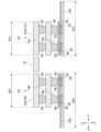
- FIG. 1 is a plan view showing a basic configuration of a digital phase shift circuit constituting a digital phase shifter according to a first embodiment of the present invention
- 2 is a cross-sectional view taken along line II-II in FIG. 1.
- 3 is a cross-sectional view taken along line III-III in FIG. 1.
- 2 is a plan view showing the connection relationship between connection pads and first and second electronic switches in the digital phase shift circuit according to the first embodiment of the present invention
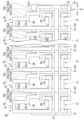
- FIG. 1 is a plan view showing a configuration of a main part of a digital phase shifter according to a first embodiment of the present invention
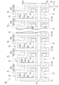
- FIG. 11 is a plan view showing a configuration of a main part of a digital phase shifter according to a second embodiment of the present invention.
- FIG. 11 is a plan view showing a configuration of a main part of a digital phase shifter according to a third embodiment of the present invention.
- Fig. 1 is a plan view showing the basic configuration of a digital phase shift circuit constituting a digital phase shifter according to a first embodiment of the present invention.
- Fig. 2 is a cross-sectional view taken along line II-II in Fig. 1.
- Fig. 3 is a cross-sectional view taken along line III-III in Fig. 1.
- the digital phase shift circuit B includes a signal line 10, a first line 21, a second line 22, an upper pad 25, a first ground conductor 31, and a second ground conductor 32.
- the first line 21 includes a first parallel line 21p1 and a pair of upper pads 21d1 and 21d2.
- the second line 22 includes a second parallel line 22p2, a first intersecting line 22c1, a third parallel line 22p3, a bent line 22b, a second intersecting line 22c2, and an upper pad 22d.
- the digital phase shift circuit B also includes first to fourth electronic switches 41 to 44, a plurality of connecting conductors 50, a capacitor 60, and a plurality of connecting pads P1 to P4 (see also FIG. 2 and FIG. 3).
- the signal line 10 is a linear strip-shaped conductor that extends in one direction. That is, the signal line 10 is a long, plate-shaped conductor with a constant width, constant thickness, and a specified length.
- a signal current flows through the signal line 10 from the left side of the paper in FIG. 1 to the right side of the paper, that is, from the end on the left side of the paper (input end) to the end on the right side of the paper (output end).
- This signal current is a high-frequency signal having a wavelength range of the microwave, quasi-millimeter wave, or millimeter wave described above.
- the direction intersecting (for example, perpendicular to) both the longitudinal direction X and the cross direction Y is referred to as the up-down direction Z.
- One direction along the up-down direction Z is referred to as the up-down or +Z direction.
- the direction opposite to the up-down is referred to as the down-down or -Z direction. Viewing from the up-down direction Z is referred to as a planar view.
- the up-down direction Z does not have to coincide with the vertical direction.
- "up" and "down” do not have to coincide with the upper and lower sides in the vertical direction.
- the +X direction and the -X direction may be defined as the left and the right, respectively.
- the second short side (-Y side) of the upper pad 21d1 is located closer to the front (-Y side) than the second side edge (-Y side) of the first parallel line 21p1.
- the dimension of the upper pad 21d1 in the cross direction Y is greater than the width (dimension in the cross direction Y) of the first parallel line 21p1.
- the second short side (-Y side) of the upper pad 21d2 is located closer to the front (-Y side) than the second side edge (-Y side) of the first parallel line 21p1.
- the dimension of the upper pad 21d2 in the cross direction Y is greater than the width (dimension in the cross direction Y) of the first parallel line 21p1.
- the second short side (+Y side) of the upper pad 22d is located further back (+Y side) than the second side edge (+Y side) of the second parallel line 22p2.
- the dimension of the upper pad 22d in the cross direction Y is greater than the width (dimension in the cross direction Y) of the second parallel line 22p2.
- the third parallel line 22p3 is a linear strip-shaped conductor connected to the first end (+Y end) of the first intersecting line 22c1.
- the third parallel line 22p3 is a long plate-shaped conductor having a constant width, a constant thickness, and a predetermined length.
- the third parallel line 22p3 extends from the first end (+Y side) of the first intersecting line 22c1 in parallel (longitudinal direction X) with the signal line 10. That is, the third parallel line 22p3 in this embodiment extends from the first end (+Y side) of the first intersecting line 22c1 toward the right side (+X side).
- the length of the third parallel line 22p3 is shorter than the length of the second parallel line 22p2.
- the ends of the third parallel line 22p3 the end located on the +X side is called the first end (one end), and the end located on the -X side is called the second end (the other end).
- the bent line 22b is a strip-shaped conductor connected to the first end (+X side) of the third parallel line 22p3 and having a bent portion CR.
- the bent line 22b is composed of a first partial line 22b1 and a second partial line 22b2.
- the first partial line 22b1 extends from the first end (+X side) of the third parallel line 22p3 so as to approach the signal line 10 in the cross direction Y.
- the ends of the first partial line 22b1 the end located on the -Y side is referred to as the first end (one end), and the end located on the +Y side is referred to as the second end (the other end).
- the second partial line 22b2 extends from the first end (-Y side) of the first partial line 22b1 in parallel to the signal line 10 (longitudinal direction X). Of the ends of the second partial line 22b2, the end located on the +X side is referred to as the first end (one end), and the end located on the -X side is referred to as the second end (the other end).
- the partial lines 22b1 and 22b2 constituting the bent line 22b are long plate-shaped conductors having a constant width, a constant thickness, and a predetermined length.
- the length of the first partial line 22b1 is shorter than the length of the first cross line 22c1.
- the first end of the second partial line 22b2 is the first end (one end) of the bent line 22b
- the second end of the first partial line 22b1 is the second end (the other end) of the bent line 22b.
- the second crossing line 22c2 extends from the first end (+X side) of the second partial line 22b2 constituting the bent line 22b toward the signal line 10 in the crossing direction Y. That is, the second crossing line 22c2 in this embodiment extends from the first end (+X end) of the bent line 22b toward the near side (-Y side). Of the ends of the second crossing line 22c2, the end located on the -Y side is referred to as the first end (one end), and the end located on the +Y side is referred to as the second end (the other end). The first end of the second crossing line 22c2 is the first end (one end) of the second line 22.
- the first edge (-Y side) of the second intersecting line 22c2 is located at approximately the same position in the intersecting direction Y as the first short side (-Y side) of the upper pad 22d and the first side edge (-Y side) of the second parallel line 22p2.
- the upper pad 22d and the second intersecting line 22c2 are arranged with a gap in the longitudinal direction X.
- the left edge (-X side) of the second intersecting line 22c2 is located at approximately the same position in the longitudinal direction X as the right edge (+X side) of the signal line 10.
- the first end (-Y side) of the second cross line 22c2 is constantly electrically connected to the second ground conductor 32 (described later) by a conductor not shown.
- the first end of the second line 22 is constantly electrically connected to the second ground conductor 32 by a conductor not shown.
- the first intersecting line 22c1, the third parallel line 22p3, the bent line 22b, and the second intersecting line 22c2 described above form a loop line that is convex toward the rear side (+Y side).
- the second short side (-Y side) of the upper pad 25 is located closer to the front (-Y side) than the second side edge (-Y side) of the first parallel line 21p1. That is, the dimension of the upper pad 25 in the cross direction Y is larger than the width (dimension in the cross direction Y) of the first parallel line 21p1, similar to the upper pads 21d1 and 21d2 that form part of the first line 21. Also, the upper pad 25 is constantly electrically connected to the second ground conductor 32 by a conductor (not shown), similar to the first end (-Y side) of the second cross line 22c2.
- the first ground conductor 31 is a plate-shaped conductor provided on the input end side (-X side) of the signal line 10.
- the first ground conductor 31 is electrically grounded.
- the first ground conductor 31 has a rectangular shape with long sides extending in the cross direction Y and short sides extending in the longitudinal direction X.
- the first ground conductor 31 also overlaps with the ends of the upper pad 21d1 and the first cross line 22c1 on the near side (-Y side) in the up-down direction Z.
- the first ground conductor 31 is located below (-Z side) the signal line 10, the first line 21 (upper pad 21d1), and the second line 22 (first cross line 22c1).
- the end located on the +Y side is called the first end (one end)
- the end located on the -Y side is called the second end (the other end).
- the first connection pad P1 includes the above-mentioned upper pad 21d1, the first intermediate pad 71a, the second intermediate pad 71b, the third intermediate pad 71c, and the first ground conductor 31.
- the upper pad 21d1, the first intermediate pad 71a, the second intermediate pad 71b, the third intermediate pad 71c, and the first ground conductor 31 overlap each other in a planar view.
- the upper pad 21d1, the first intermediate pad 71a, the second intermediate pad 71b, the third intermediate pad 71c, and the first ground conductor 31 are arranged in this order from the upper side (+Z side) to the lower side (-Z side), and are spaced apart in the vertical direction Z.
- connection conductor 50 is a conductor that extends in the vertical direction Z and electrically and mechanically connects a member connected to the upper end of the connection conductor 50 with a member connected to the lower end of the connection conductor 50.
- the connection conductor 50 is, for example, a via that penetrates an insulating layer (not shown) in the vertical direction Z.
- the second connection pad P2 includes the front side (-Y side) end of the first intersecting line 22c1, the first intermediate pad 72a, the second intermediate pad 72b, the third intermediate pad 72c, and the first ground conductor 31.
- the front side (-Y side) end of the first intersecting line 22c1, the first intermediate pad 72a, the second intermediate pad 72b, the third intermediate pad 72c, and the first ground conductor 31 overlap each other in a plan view.
- the end of the first cross line 22c1 on the near side (-Y side) and the first intermediate pad 72a are electrically and mechanically connected by a plurality of connecting conductors 50.
- the first intermediate pad 72a and the second intermediate pad 72b are electrically and mechanically connected by a plurality of connecting conductors 50.
- the second intermediate pad 72b and the third intermediate pad 72c are electrically and mechanically connected by a plurality of connecting conductors 50.
- the third intermediate pad 72c and the first ground conductor 31 are electrically and mechanically connected by a plurality of connecting conductors 50.
- the second connection pad P2 constantly electrically connects the first end (-X side) of the second parallel line 22p2 and the first ground conductor 31.
- the third connection pad P3 includes the upper pad 21d2, the first intermediate pad 73a, the second intermediate pad 73b, the third intermediate pad 73c, and the lower pad 33a.
- the upper pad 21d2, the first intermediate pad 73a, the second intermediate pad 73b, the third intermediate pad 73c, and the lower pad 33a overlap each other in a planar view.
- the upper pad 21d2, the first intermediate pad 73a, the second intermediate pad 73b, the third intermediate pad 73c, and the lower pad 33a are arranged in this order from the upper side (+Z side) to the lower side (-Z side), and are spaced apart in the vertical direction Z.
- the lower pad 33a (first lower pad) is a rectangular flat conductor whose long sides extend in the transverse direction Y and whose short sides extend in the longitudinal direction X.
- the short side located on the +Y side is referred to as the first short side (one short side)
- the short side located on the -Y side is referred to as the second short side (the other short side).
- the lower pad 33a is provided separately from the second grounding conductor 32.
- the lower pad 33a and the second grounding conductor 32 are electrically connected or not connected depending on the state of the first electronic switch 41 (described later). Therefore, the lower pad 33a is electrically grounded or not connected depending on the state of the first electronic switch 41.
- the upper pad 21d2 and the first intermediate pad 73a are electrically and mechanically connected by a plurality of connecting conductors 50.
- the first intermediate pad 73a and the second intermediate pad 73b are electrically and mechanically connected by a plurality of connecting conductors 50.
- the second intermediate pad 73b and the third intermediate pad 73c are electrically and mechanically connected by a plurality of connecting conductors 50.
- the third intermediate pad 73c and the lower pad 33a are electrically and mechanically connected by a plurality of connecting conductors 50.
- the third connection pad P3 constantly electrically connects the second end (+X side) of the first parallel line 21p1 and the first electronic switch 41.
- the fourth connection pad P4 includes the upper pad 22d, the first intermediate pad 74a, the second intermediate pad 74b, the third intermediate pad 74c, and the lower pad 33b.
- the upper pad 22d, the first intermediate pad 74a, the second intermediate pad 74b, the third intermediate pad 74c, and the lower pad 33b overlap each other in a planar view.
- the upper pad 22d, the first intermediate pad 74a, the second intermediate pad 74b, the third intermediate pad 74c, and the lower pad 33b are arranged in this order from the upper side (+Z side) to the lower side (-Z side), and are spaced apart in the vertical direction Z.
- the lower pad 33b (second lower pad) is a rectangular flat conductor whose long sides extend in the transverse direction Y and whose short sides extend in the longitudinal direction X.
- the short side located on the +Y side is referred to as the first short side (one short side)
- the short side located on the -Y side is referred to as the second short side (the other short side).
- the lower pad 33b is provided separately from the second grounding conductor 32 and the lower pad 33a.
- the lower pad 33b and the second grounding conductor 32 are electrically connected or not connected depending on the state of the second electronic switch 42 (described later). Therefore, the lower pad 33b is electrically grounded or not connected depending on the state of the second electronic switch 42.
- the upper pad 22d and the first intermediate pad 74a are electrically and mechanically connected by a plurality of connecting conductors 50.
- the first intermediate pad 74a and the second intermediate pad 74b are electrically and mechanically connected by a plurality of connecting conductors 50.
- the second intermediate pad 74b and the third intermediate pad 74c are electrically and mechanically connected by a plurality of connecting conductors 50.
- the third intermediate pad 74c and the lower pad 33b are electrically and mechanically connected by a plurality of connecting conductors 50.
- the fourth connection pad P4 constantly electrically connects the second end (+X side) of the second parallel line 22p2 and the second electronic switch 42.
- the dimension D12 in the cross direction Y of the lower pad 33a forming part of the connection pad P3 is larger than the dimension D11 in the cross direction Y of the upper pad 21d2 forming part of the connection pad P3.
- the dimension D22 in the cross direction Y of the lower pad 33b forming part of the connection pad P4 is larger than the dimension D21 in the cross direction Y of the upper pad 22d forming part of the connection pad P4.
- the capacitor 60 is a parallel plate whose upper electrode is connected to the signal line 10 and whose lower electrode is connected to the first ground conductor 31 via the third electronic switch 43.
- the capacitor 60 has a capacitance Ca according to the opposing area of the parallel plates.
- the capacitance Ca is a circuit constant provided between the signal line 10 and the first ground conductor 31.
- the capacitor 60 may also be a comb-tooth capacitor.
- the first electronic switch 41 is a transistor that freely connects the lower pad 33a of the third connection pad P3 and the second ground conductor 32.
- the first electronic switch 41 in this embodiment is, for example, a MOS type FET, with a drain terminal connected to the lower pad 33a of the third connection pad P3, a source terminal connected to the second ground conductor 32, and a gate terminal connected to the switch control unit 80.
- the first electronic switch 41 switches the conductive state between the drain terminal and the source terminal to an open state or a closed state based on a gate signal input to the gate terminal from the switch control unit 80. That is, the first electronic switch 41 uses the switch control unit 80 to bring the second end (+X side) of the first parallel line 21p1 and the second ground conductor 32 into a conductive state or a cut-off state.
- the second electronic switch 42 is a transistor that can be freely opened and closed by connecting the lower pad 33b of the fourth connection pad P4 and the second ground conductor 32.
- the second electronic switch 42 in this embodiment is, for example, a MOS type FET, with a drain terminal connected to the lower pad 33b of the fourth connection pad P4, a source terminal connected to the second ground conductor 32, and a gate terminal connected to the switch control unit 80.
- the second electronic switch 42 switches the conductive state between the drain terminal and the source terminal to an open state or a closed state based on a gate signal input to the gate terminal from the switch control unit 80. That is, the second electronic switch 42 uses the switch control unit 80 to bring the second end (+X side) of the second parallel line 22p2 and the second ground conductor 32 into a conductive state or a cut-off state.
- FIG. 4 is a plan view showing the connection relationship between the connection pads and the first and second electronic switches in the digital phase shift circuit according to the first embodiment of the present invention.
- the first electronic switch 41 and the second electronic switch 42 are, for example, MOS type FETs having a rectangular shape in a plan view, and have a drain terminal DT and a source terminal ST. Note that the gate terminal is not shown in FIG. 4.
- the size (specifically, the gate width W) of the first electronic switch 41 and the second electronic switch 42 is increased to reduce the loss of high-frequency signals.
- the size of the first electronic switch 41 and the second electronic switch 42 is increased, the length of the drain terminal DT and the source terminal ST in the cross direction Y also increases, as shown in FIG. 4.
- the dimension D12 of the lower pad 33a in the cross direction Y is made longer to match the length of the drain terminal DT of the first electronic switch 41 in the cross direction Y.
- the dimension D12 of the lower pad 33a in the cross direction Y is made larger than the dimension D11 of the upper pad 21d2 in the cross direction Y. This allows the entire drain terminal DT of the first electronic switch 41 to be connected to the lower pad 33a.
- the dimension D22 of the lower pad 33b in the cross direction Y is made longer to match the length of the drain terminal DT of the second electronic switch 42 in the cross direction Y.
- the dimension D22 of the lower pad 33b in the cross direction Y is made larger than the dimension D21 of the upper pad 22d in the cross direction Y. This allows the entire drain terminal DT of the second electronic switch 42 to be connected to the lower pad 33b.
- the second short side (-Y side) of the second ground conductor 32 is located at approximately the same position in the cross direction Y as the second short side (-Y side) of the lower pad 33a.
- the second ground conductor 32 extends in the cross direction Y from the first short side (+Y side) of the lower pad 33b to the second short side (-Y side) of the lower pad 33a. Therefore, as shown in FIG. 4, the source terminals ST of the first electronic switch 41 and the second electronic switch 42 are also entirely connected to the second ground conductor 32.
- the third electronic switch 43 is a transistor that freely connects the lower electrode of the capacitor 60 and the first ground conductor 31.
- the third electronic switch 43 is, for example, a MOS type FET, with a drain terminal connected to the lower electrode of the capacitor 60, a source terminal connected to the first ground conductor 31, and a gate terminal connected to the switch control unit 80.
- the third electronic switch 43 is disposed at a position away from the signal line 10 toward the rear (+Y side). Also, the first end (+Y side) of the first ground conductor 31 extends away from the signal line 10 in the cross direction Y and is connected to the third electronic switch 43.
- the reason for this arrangement is that there are design rule restrictions on the connection of the lower electrode of the capacitor 60 in certain semiconductor manufacturing equipment.
- the lower electrode of the capacitor 60 is restricted to first be connected to an upper wiring layer (e.g., the layer in which the signal line 10 is formed) via a connection wire and a via, and then connected from that wiring layer to a lower wiring layer via a via.
- an upper wiring layer e.g., the layer in which the signal line 10 is formed
- the connection path between the lower electrode of the capacitor 60 and the third electronic switch 43 is illustrated in a simplified manner. Due to this restriction, the third electronic switch 43 cannot be placed near the position where the capacitor 60 is formed (e.g., the input end side (-X side) of the signal line 10 shown in FIG. 1), and must be placed at a position away from the signal line 10 toward the rear (+Y side).
- the first ground conductor 31 extends away from the signal line 10 in the cross direction Y in order to be connected to the source terminal of the third electronic switch 43 placed in such a position.
- the third electronic switch 43 switches the conductive state between the drain terminal and the source terminal to an open state or a closed state based on a gate signal input to the gate terminal from the switch control unit 80. That is, the third electronic switch 43 uses the switch control unit 80 to bring the lower electrode of the capacitor 60 and the first ground conductor 31 into a conductive state or a cut-off state.
- the size (gate width) of the first electronic switch 41 and the second electronic switch 42 is set to, for example, at least twice the size (gate width) of the third electronic switch 43. It is preferable that the size (gate width) of the first electronic switch 41 and the second electronic switch 42 is at least five times the size (gate width) of the third electronic switch 43.
- the loss of the high frequency signal in the high delay mode can be significantly reduced. Since it is desirable for the difference between the loss of the high frequency signal in the high delay mode and the loss of the high frequency signal in the low delay mode to be as small as possible, if the loss of the high frequency signal in the high delay mode is reduced, it is also necessary to reduce the loss of the high frequency signal in the low delay mode. For this reason, the size of the first electronic switch 41 and the second electronic switch 42 is made larger than the size of the third electronic switch 43.
- the size of the first electronic switch 41 and the second electronic switch 42 must be set to at least twice the size of the third electronic switch 43. Furthermore, if the size of the first electronic switch 41 and the second electronic switch 42 is set to at least five times the size of the third electronic switch 43, the high-frequency signal loss in the high-latency mode and the low-latency mode can be made to be approximately the same.
- the fourth electronic switch 44 is a transistor that freely connects the input end side (-X side) of the signal line 10 and the first ground conductor 31.
- the fourth electronic switch 44 is a MOS type FET, like the first electronic switch 41, the second electronic switch 42, and the third electronic switch 43 described above, and has a drain terminal connected to the input end side (-X side) of the signal line 10, a source terminal connected to the first ground conductor 31, and a gate terminal connected to the switch control unit 80.
- the fourth electronic switch 44 may be provided between the output end side (+X side) of the signal line 10 and the second ground conductor 32, instead of between the input end side (-X side) of the signal line 10 and the first ground conductor 31.
- the fourth electronic switch 44 switches the conduction state between the drain terminal and the source terminal to an open state or a closed state based on a gate signal input to the gate terminal from the switch control unit 80. That is, the fourth electronic switch 44 uses the switch control unit 80 to establish a conduction state or a cutoff state between the input end side (-X side) of the signal line 10 and the first ground conductor 31.
- the switch control unit 80 is a control circuit that controls the above-mentioned first electronic switch 41, second electronic switch 42, third electronic switch 43, and fourth electronic switch 44.
- the switch control unit 80 has four output ports, and outputs gate signals individually from each output port to the gate terminals of the first electronic switch 41, second electronic switch 42, third electronic switch 43, and fourth electronic switch 44. That is, the switch control unit 80 opens or closes the first electronic switch 41, second electronic switch 42, third electronic switch 43, and fourth electronic switch 44 using the gate signals.
- the digital phase shift circuit B switches between operating modes depending on the conductive states of the first to third electronic switches 41 to 43. That is, the operating modes of the digital phase shift circuit B include a low-delay mode in which the first electronic switch 41 and the second electronic switch 42 are set to a closed state by the switch control unit 80, and the third electronic switch 43 is set to an open state, and a high-delay mode in which the first electronic switch 41 and the second electronic switch 42 are set to an open state by the switch control unit 80, and the third electronic switch 43 is set to a closed state.
- the switch control unit 80 sets the first electronic switch 41 and the second electronic switch 42 to a closed state, and sets the third electronic switch 43 to an open state. That is, in the low delay mode, the phase at the output end (right end) becomes a first phase ⁇ L smaller than the second phase ⁇ H in the high delay mode due to a first propagation delay time T L until the high frequency signal propagates from the input end (left end) to the output end (right end ) of the signal line 10.
- T L first propagation delay time
- the first electronic switch 41 When the first electronic switch 41 is set to a closed state, the second end (+X side) of the first parallel line 21p1 is connected to the second ground conductor 32 via the third connection pad P3 (see FIG. 1). Meanwhile, the first end (-X side) of the first parallel line 21p1 is constantly connected to the first ground conductor 31 via the first connection pad P1 (see FIGS. 1 and 2). Therefore, the first parallel line 21p1 forms a first current path through which a current can flow between the first end (-X side) and the second end (+X side) by connecting the second end (+X side) to the second ground conductor 32 via the first electronic switch 41.
- the second end (+X side) of the second parallel line 22p2 is connected to the second ground conductor 32 via the fourth connection pad P4 (see FIG. 1).
- the first end (-X side) of the second parallel line 22p2 is constantly connected to the first ground conductor 31 via the second connection pad P2 (see FIGS. 1 and 2). Therefore, by connecting the second end (+X side) of the second parallel line 22p2 to the second ground conductor 32 via the second electronic switch 42, a second current path is formed through which a current can flow between the first end (-X side) and the second end (+X side).
- a first return current flows in the opposite direction to the direction of the signal current due to the passage of the signal current in the signal line 10.
- a second return current flows in the opposite direction to the direction of the signal current, i.e., in the same direction as the first return current, due to the passage of the signal current in the signal line 10.
- the first return current flowing through the first parallel line 21p1 and the second return current flowing through the second parallel line 22p2 are both opposite to the direction of the signal current. Therefore, the first return current and the second return current act to reduce the overall inductance of the digital phase shift circuit B due to the electromagnetic coupling (mutual induction) between the signal line 10 and the first parallel line 21p1 and the electromagnetic coupling (mutual induction) between the signal line 10 and the second parallel line 22p2.
- the inductance of the signal line 10 is Ls low
- the inductance of the return path (the first parallel line 21p1 and the second parallel line 22p2) is Lg low
- the mutual inductance between the signal line 10 and the return path is M low .
- the overall inductance L low of the digital phase shift circuit B in the low delay mode is Ls low +Lg low -M low .
- the signal line 10 has the capacitance C1 as a parasitic capacitance.
- the third electronic switch 43 is set to an open state, and therefore the capacitor 60 is not connected between the signal line 10 and the first ground conductor 31. That is, the capacitance Ca of the capacitor 60 does not affect the high-frequency signal propagating through the signal line 10. Therefore, a first propagation delay time T L proportional to (L low ⁇ C1) 1/2 acts on the high-frequency signal propagating through the signal line 10.
- the high frequency signal at the output end of the signal line 10 lags behind the high frequency signal at the input end of the signal line 10 by a first phase ⁇ L. That is, in the low delay mode, the first return current and the second return current cause the overall inductance of the digital phase shift circuit B to become the inductance L low , thereby reducing the propagation delay time.
- the switch control unit 80 sets the first electronic switch 41 and the second electronic switch 42 to an open state, and sets the third electronic switch 43 to a closed state.
- the fourth electronic switch 44 is set to an open state. That is, in the high delay mode, the phase at the output end (right end) becomes a second phase ⁇ H that is larger than the first phase ⁇ L in the low delay mode due to the second propagation delay time T H until the high frequency signal propagates from the input end (left end) of the signal line 10 to the output end (right end).
- the high delay mode will be described in more detail below.
- the first electronic switch 41 and the second electronic switch 42 are set to an open state. Therefore, the first conductive path described above is not formed in the first parallel line 21p1, and the second conductive path described above is not formed in the second parallel line 22p2. Therefore, the first return current flowing in the first parallel line 21p1 becomes extremely small, and the second return current flowing in the second parallel line 22p2 becomes extremely small.
- the near side (-Y side) end of the first cross line 22c1 is constantly connected to the first ground conductor 31 via the second connection pad P2 (see FIG. 2).
- the first end (-Y side) of the second cross line 22c2 is constantly connected to the second ground conductor 32, as described above. Therefore, a third current path through which a current can flow between the first end (-Y side) of the second cross line 22c2 and the near side (-Y side) end of the first cross line 22c1 is formed in advance in the first cross line 22c1, the third parallel line 22p3, the bent line 22b, and the second cross line 22c2.
- a third return current flows from the first end (-Y side) of the second crossing line 22c2 to the near end (-Y side) of the first crossing line 22c1 via the bent line 22b and the third parallel line 22p3.
- the third return current flows in the third parallel line 22p3 parallel to the signal line 10 and the second partial line 22b2 of the bent line 22b in a direction opposite to the direction of current flow of the signal current in the signal line 10.
- the first partial line 22b1 of the bent line 22b, the third parallel line 22p3, and the first cross line 22c1 form a loop line that is convex on the opposite side (+Y side) from the signal line 10. Therefore, the inductance of the return path (path through which the third return current flows) can be increased compared to a conventional configuration in which the return path does not form a loop line. This allows the overall inductance of the digital phase shift circuit B to be increased.
- the inductance of the signal line 10 is Ls high
- the inductance of the return path (the second intersecting line 22c2, the bent line 22b, the third parallel line 22p3, and the first intersecting line 22c1)
- Lg high Ls low
- M high M high
- Ls high Ls low
- the total inductance L high of the digital phase shift circuit B in the high delay mode is Ls high +Lg high -M high .
- Lg low ⁇ Lg high and M low >M high , and therefore L high >L low .
- the principle by which the third return current acts to increase the inductance of the return path can be explained as follows. That is, the magnetic field generated when the third return current flows through the first partial line 22b1 of the curved line 22b, the magnetic field generated when the third return current flows through the third parallel line 22p3, and the magnetic field generated when the third return current flows through the first intersecting line 22c1 all have the same direction (+Z direction) within the above-mentioned loop line. Therefore, these magnetic fields reinforce each other. Therefore, compared to the conventional configuration in which the line through which the third return current flows does not form a loop line, the magnetic field generated by the third return current can be made larger, and the inductance of the return path can be increased.
- the value of the inductance of the return path can be significantly changed by adjusting the height of the loop (i.e., the position of the third parallel line 22p3 in the intersecting direction Y, as well as the first intersecting line 22c1 and the first partial line 22b1 of the curved line 22b.
- the signal line 10 has a capacitance C1 as a parasitic capacitance.
- the third electronic switch 43 is set to a closed state, and therefore the capacitor 60 is connected between the signal line 10 and the first ground conductor 31. That is, the signal line 10 has a capacitance Cb which is a sum of the capacitance Ca of the capacitor 60 and the capacitance C1 (parasitic capacitance). Therefore, a second propagation delay time T H related to the increase in inductance of the transmission system and the sum of the capacitance Cb acts on the high frequency signal propagating through the signal line 10.
- the high frequency signal at the output end of the signal line 10 lags behind the high frequency signal at the input end of the signal line 10 by the second phase ⁇ H. That is, in the high delay mode, the inductance of the transmission system is increased due to the third return current, thereby increasing the propagation delay time.
- the loss in the signal line 10 may be intentionally increased by setting the electronic switch 44 to a closed state. This loss is intended to make the loss of the high frequency signal in the high delay mode the same as the loss of the high frequency signal in the low delay mode.
- Digital Phase Shifter Fig. 5 is a plan view showing the main configuration of a digital phase shifter according to a first embodiment of the present invention.
- a digital phase shifter A1 of this embodiment has a plurality of digital phase shift circuits B1 , B2 , B3 , ..., Bn -1 , Bn cascaded in the longitudinal direction X.
- the basic configuration of the digital phase shift circuits B1 , B2 , B3 , ..., Bn -1 , Bn is the same as that of the digital phase shift circuit B described using Figs. 1 to 4.
- the digital phase shifter A1 outputs the high frequency signal input from the digital phase shift circuit B1 from the digital phase shift circuit Bn , or outputs the high frequency signal input from the digital phase shift circuit Bn from the digital phase shift circuit B1 .
- the following description will be given taking as an example a case where the high frequency signal input from the digital phase shift circuit B1 is output from the digital phase shift circuit Bn .
- the first electronic switch 41, the second electronic switch 42, and the switch control section 80 are omitted from Fig. 5 and subsequent figures.
- the digital phase shift circuits B 1 , B 2 , B 3 , ..., B n-1 , B n are cascaded in the longitudinal direction X such that the first lines 21 of all the digital phase shift circuits B 1 , B 2 , B 3 , ..., B n-1 , B n are located on the second side (-Y side) of the signal line 10, and the second lines 22 of all the digital phase shift circuits B 1 , B 2 , B 3 , ..., B n-1 , B n are located on the first side (+Y side) of the signal line 10.
- the digital phase shifter A1 is configured such that the loop line is disposed only on the first side (+Y side) of the signal line 10. The reason for this configuration is to reduce the size of the digital phase shifter A1.
- the digital phase shift circuits B 1 to B n-1 are connected to the adjacent digital phase shift circuits B 2 to B n on the right side (+X side) so that a portion of each of them extends into the adjacent digital phase shift circuits B 2 to B n. It can also be said that in the digital phase shifter A1 according to this embodiment, the digital phase shift circuits B 2 to B n are connected to the adjacent digital phase shift circuits B 1 to B n-1 on the left side (-X side) so that a portion of each of them extends into the adjacent digital phase shift circuits B 2 to B n.
- the first ground conductor 31 and the second ground conductor 32 are commonized, a portion of the first cross line 22c1 and the second cross line 22c2 are commonized, and the upper pad 21d1 and the upper pad 25 are commonized. That is, among the adjacent digital phase shift circuits B, the first ground conductor 31 of one digital phase shift circuit B and the second ground conductor 32 of the other digital phase shift circuit B are commonized, a portion of the first cross line 22c1 of one digital phase shift circuit B and the second cross line 22c2 of the other digital phase shift circuit B are commonized, and the upper pad 21d1 of one digital phase shift circuit B and the upper pad 25 of the other digital phase shift circuit B are commonized.
- the second ground conductor 32 of the digital phase shift circuit B1 and the first ground conductor 31 of the digital phase shift circuit B2 are shared, the second crossing line 22c2 of the digital phase shift circuit B1 and a part of the first crossing line 22c1 of the digital phase shift circuit B2 are shared, and the upper pad 25 of the digital phase shift circuit B1 and the upper pad 21d1 of the digital phase shift circuit B2 are shared.
- the first ground conductor 31 of the digital phase shift circuit B2 also functions as the second ground conductor 32 of the digital phase shift circuit B1 .
- a part of the first cross line 22c1 of the digital phase shift circuit B2 also functions as the second cross line 22c2 of the digital phase shift circuit B1 .
- the upper pad 21d1 of the digital phase shift circuit B2 also functions as the upper pad 25 of the digital phase shift circuit B1 .
- the bent line 22b of the second line 22 is connected to the first cross line 22c1 of the second line 22 in the adjacent digital phase shift circuit B. That is, among the adjacent digital phase shift circuits B, the bent line 22b of the second line 22 of one digital phase shift circuit B is connected to the first cross line 22c1 of the second line 22 of the other digital phase shift circuit B.
- the bent line 22b of the second line 22 is connected perpendicularly to the first cross line 22c1 of the second line 22 in the adjacent digital phase shift circuit B.
- the second partial line 22b2 forming the bent line 22b of the second line 22 in the digital phase shift circuit B1 is connected perpendicularly to the first cross line 22c1 of the second line 22 in the digital phase shift circuit B2 .
- the line through which the third return current flows forms a loop line that is convex on the opposite side (+Y side) of the signal line 10. This makes it possible to increase the efficiency of generating a magnetic field compared to the conventional technique. Also, in the digital phase shifter A1 of the present embodiment, as described above, it is possible to reduce the mutual inductance between adjacent digital phase shift circuits B. As a result, the digital phase shifter A1 of the present embodiment can ensure a required amount of phase shift even in a configuration in which a loop line is arranged only on the first side (+Y side) of the signal line 10.
- the digital phase shifter A1 of this embodiment for example, when the adjacent digital phase shift circuits, except for the digital phase shift circuit B1 , are set to the high delay mode, the third return current flows through a path that does not pass through the second connection pad P2.
- the digital phase shift circuits B1 to B3 are set to the high delay mode, the third return current flows through the path PT in the figure without passing through obstacles with large losses, such as the second connection pad P2 of the digital phase shift circuits B2 and B3 and the first ground conductor 31 (second ground conductor 32). Therefore, the digital phase shifter A1 of this embodiment can significantly reduce the loss of the high-frequency signal in the high delay mode.
- the digital phase shifter A1 of this embodiment can significantly reduce the loss of the high frequency signal in the high delay mode.
- the size of the first electronic switch 41 and the second electronic switch 42 arranged in the current paths of the first return current and the second return current in the low delay mode can be increased. This is because it is desirable for the difference between the loss of the high frequency signal in the high delay mode and the loss of the high frequency signal in the low delay mode to be as small as possible, and therefore if the loss of the high frequency signal in the high delay mode is reduced, it is also necessary to reduce the loss of the high frequency signal in the low delay mode. In this way, the digital phase shifter A1 of this embodiment can reduce the loss of the high frequency signal overall.
- the digital phase shifter A1 of this embodiment is a phase shifter having a plurality of digital phase shift circuits B1 to Bn connected in cascade.
- Each of the plurality of digital phase shift circuits B1 to Bn includes a signal line 10, a first line 21, a second line 22, a first ground conductor 31, a second ground conductor 32, a first electronic switch 41, and a second electronic switch 42.
- the first line 21 includes a first parallel line 21p1 extending parallel to the signal line 10.
- the second line 22 includes a second parallel line 22p2 extending parallel to the signal line 10, a first intersecting line 22c1 extending from a first end of the second parallel line 22p2 away from the signal line 10 in a crossing direction Y that intersects with the longitudinal direction of the signal line 10, a third parallel line 22p3 extending parallel to the signal line 10 from the first end of the first intersecting line 22c1 and having a length shorter than the second parallel line 22p2, and a bent line 22b connected to the first end of the third parallel line 22p3 and having a bent portion CR formed therein, the bent line 22b extending shorter than the length of the first intersecting line 22c1 so as to approach the signal line 10 in the crossing direction Y and then extending parallel to the signal line 10 in the crossing direction Y.
- Each of the digital phase shift circuits B 1 to B n includes a first ground conductor 31, a second ground conductor 32, a first electronic switch 41, and a second electronic switch 42.
- the first ground conductor 31 is electrically connected to a first end of the first parallel line 21p1 and a first end of the second parallel line 22p2, and the second ground conductor 32 is connected to a first end of the second line 22.
- the first electronic switch 41 is provided between a second end of the first parallel line 21p1 and the second ground conductor 32
- the second electronic switch 42 is provided between a second end of the second parallel line 22p2 and the second ground conductor 32.
- the signal line 10 is located between the first parallel line 21p1 and the second parallel line 22p2.
- the first ground conductor 31 and the second ground conductor 32 are shared in a portion where the digital phase shift circuits are adjacent to each other.
- the bent line 22b of the second line 22 is connected to the first cross line 22c1 of the second line 22 in the adjacent digital phase shift circuit.
- Second Embodiment Digital Phase Shifter Fig. 6 is a plan view showing the main configuration of a digital phase shifter according to a second embodiment of the present invention.
- the digital phase shifter A2 of this embodiment has a configuration generally similar to that of the digital phase shifter A1 shown in Fig. 5, but the basic configurations of the digital phase shift circuits B1 , B2 , B3 , ..., Bn -1 , Bn are slightly different from those of the digital phase shift circuit shown in Fig. 5.
- the bent line 22b of the second line 22 is made up of first to fourth partial lines 22b1, 22b2 , 22b3 , and 22b4. Note that three or more bends CR may be formed in the bent line 22b of the second line 22.
- the first partial line 22b1 is a line that extends from the first end (+X side) of the third parallel line 22p3 to a length shorter than the first intersecting line 22c1 so as to approach the signal line 10 in the intersecting direction Y.
- the second partial line 22b2 is a line that extends from the first end (-Y side) of the first partial line 22b1 in parallel to the signal line 10 (longitudinal direction X) to a length shorter than the second parallel line 22p2.
- the third partial line 22b3 is a line that extends from the first end (+X side) of the second partial line 22b2 to a length shorter than the first intersecting line 22c1 so as to approach the signal line 10 in the intersecting direction Y.
- the fourth partial line 22b4 is a line that extends parallel to the signal line 10 (longitudinal direction X) from the first end (-Y side) of the third partial line 22b3, the length of which is shorter than the length of the second parallel line 22p2.
- the partial lines 22b1, 22b2, 22b3, and 22b4 that form the bent line 22b are each a long, plate-shaped conductor with a constant width, a constant thickness, and a predetermined length.
- the bent line 22b of the second line 22 included in the digital phase shift circuits B 1 , B 2 , B 3 , ..., B n-1 , B n has two bends CR. This allows the phase shift amount to be greater than that of the digital phase shifter A1 of the first embodiment. Note that, in the present embodiment, an example has been described in which the bent line 22b of the second line 22 included in the digital phase shift circuits B 1 , B 2 , B 3 , ..., B n-1 , B n has two bends CR, but the bent line 22b may have three or more bends CR.
- the digital phase shifter A2 of this embodiment has a different number of bends CR formed in the bent line 22b, but is basically configured in the same manner as the digital phase shifter A1 shown in FIG. 5. Therefore, like the digital phase shifter A1 shown in FIG. 5, it is possible to achieve the desired phase shifting characteristics while being smaller than conventional ones.
- FIG. 7 is a plan view showing the main configuration of a digital phase shifter according to a third embodiment of the present invention.
- the digital phase shifter A3 of this embodiment has a configuration generally similar to that of the digital phase shifter A1 shown in Fig. 5, but the configurations of the digital phase shift circuits B1 , B2 , B3 , ..., Bn-1 , Bn are slightly different from those of the digital phase shifter shown in Fig. 5.
- the distance D1 (see FIG. 1) between the center line of the second parallel line 22p2 and the center line of the third parallel line 22p3 in the cross direction Y is different between adjacent digital phase shift circuits.
- the distance D1 in the even-numbered digital phase shift circuits (digital phase shift circuits B 2 , B 4 , B 6 , ...) is set shorter than the distance D1 in the odd-numbered digital phase shift circuits (digital phase shift circuits B 1 , B 3 , B 5 , ).
- the digital phase shifter A3 of this embodiment can have a larger phase shift amount than the digital phase shifter A1 of the first embodiment.
- the digital phase shifter A3 of this embodiment has a fundamentally similar configuration to the digital phase shifter A1 shown in FIG. 5, although the distance D1 (see FIG. 1) between the center line of the second parallel line 22p2 and the center line of the third parallel line 22p3 in the cross direction Y is different in adjacent digital phase shift circuits. Therefore, like the digital phase shifter A1 shown in FIG. 5, it is possible to achieve the desired phase shifting characteristics in a smaller size than conventional devices.
- the distance D1 (see FIG. 1) between the center line of the second parallel line 22p2 and the center line of the third parallel line 22p3 in the cross direction Y is different in adjacent digital phase shift circuits.
- the distance D1 does not necessarily need to be different in adjacent digital phase shift circuits. It is sufficient that the distance D1 in at least one digital phase shift circuit is different from the distance D1 in the other digital phase shift circuits.
- the distance D1 is not limited to two types, and may be three or more types.
- the digital phase shifter according to the embodiment of the present invention has been described above, the present invention is not limited to the above embodiment and can be freely modified within the scope of the present invention.
- the second embodiment and the third embodiment may be combined. That is, in the digital phase shifter A2 shown in FIG. 6, the distance between the center line of the second parallel line 22p2 and the center line of the third parallel line 22p3 in the cross direction Y of the digital phase shift circuits B 1 , B 2 , B 3 , ..., B n-1 , B n may be made different in adjacent digital phase shift circuits.
Landscapes
- Semiconductor Integrated Circuits (AREA)
Abstract
Description
本願は、2023年06月07日に、日本に出願された特願2023-093906号に基づき優先権を主張し、その内容をここに援用する。
〈デジタル移相回路〉
図1は、本発明の第1実施形態によるデジタル移相器を構成するデジタル移相回路の基本構成を示す平面図である。図2は、図1中のII-II線に沿う断面矢視図である。図3は、図1中のIII-III線に沿う断面矢視図である。
なお、上下方向Zは鉛直方向と一致していなくてもよい。また、「上方」および「下方」は、鉛直方向における上側および下側と一致していなくてもよい。また、+Xの向きおよび-Xの向きをそれぞれ右方および左方と定義する代わりに、+Xの向きおよび-Xの向きをそれぞれ左方および右方としてもよい。
図5は、本発明の第1実施形態によるデジタル移相器の要部構成を示す平面図である。図5に示す通り、本実施形態のデジタル移相器A1は、複数のデジタル移相回路B1,B2,B3,…,Bn-1,Bnを長手方向Xに縦続接続したものである。尚、デジタル移相回路B1,B2,B3,…,Bn-1,Bnの基本構成は、図1~図4を用いて説明したデジタル移相回路Bと同様である。
〈デジタル移相器〉
図6は、本発明の第2実施形態によるデジタル移相器の要部構成を示す平面図である。図6に示す通り、本実施形態のデジタル移相器A2は、図5に示すデジタル移相器A1と概ね同様の構成であるが、デジタル移相回路B1,B2,B3,…,Bn-1,Bnの基本構成が、図5に示すデジタル移相回路と若干異なる。
〈デジタル移相器〉
図7は、本発明の第3実施形態によるデジタル移相器の要部構成を示す平面図である。図7に示す通り、本実施形態のデジタル移相器A3は、図5に示すデジタル移相器A1と概ね同様の構成であるが、デジタル移相回路B1,B2,B3,…,Bn-1,Bnの構成が、図5に示すデジタル移相回路と若干異なる。
Claims (8)
- 縦続接続された複数のデジタル移相回路を有する移相器であって、
前記デジタル移相回路は、
信号線路と、
前記信号線路と平行に延びる第1平行線路を含む第1線路と、
前記信号線路と平行に延びる第2平行線路と、前記第2平行線路の第1の端部から前記信号線路の長手方向と交差する交差方向において前記信号線路から遠ざかるように延びる第1交差線路と、前記第1交差線路の第1の端部から前記信号線路と平行に延び、前記第2平行線路の長さより短い第3平行線路と、前記第3平行線路の第1の端部に接続され、前記交差方向において前記信号線路に近づくように前記第1交差線路の長さより短く延びてから前記信号線路と平行に延びる屈曲部が形成された屈曲線路と、を含む第2線路と、
前記第1平行線路の第1の端部及び前記第2平行線路の第1の端部に電気的に接続された第1接地導体と、
前記第2線路の第1の端部に接続された第2接地導体と、
前記第1平行線路の第2の端部と前記第2接地導体との間に設けられた第1電子スイッチと、
前記第2平行線路の第2の端部と前記第2接地導体との間に設けられた第2電子スイッチと、を備え、
前記第1平行線路と前記第2平行線路との間に前記信号線路が位置し、
前記デジタル移相回路が隣り合う部分において、前記第1接地導体と前記第2接地導体とが共通化されており、
前記デジタル移相回路が隣り合う部分において、前記第2線路の前記屈曲線路は、隣り合う前記デジタル移相回路における前記第2線路の前記第1交差線路に接続されている、
デジタル移相器。 - 前記デジタル移相回路が隣り合う部分において、前記第2線路の前記屈曲線路は、隣り合う前記デジタル移相回路における前記第2線路の前記第1交差線路に対して垂直に接続されている、請求項1記載のデジタル移相器。
- 前記信号線路の第1の端部に接続されたコンデンサと、
前記コンデンサと前記第1接地導体との間に設けられた第3電子スイッチと、
を更に備え、
前記第1接地導体の第1の端部は、前記交差方向において前記信号線路から遠ざかるように延びて前記第3電子スイッチに接続されている、
請求項1または2記載のデジタル移相器。 - 前記第1電子スイッチ、前記第2電子スイッチ、及び前記第3電子スイッチは、電界効果トランジスタであり、
前記第1電子スイッチ及び前記第2電子スイッチをなす電界効果トランジスタのサイズは、前記第3電子スイッチをなす電界効果トランジスタのサイズの2倍以上である、
請求項3記載のデジタル移相器。 - 前記第1平行線路の第2の端部に設けられた第1上側パッドと、
前記第2平行線路の第2の端部に設けられた第2上側パッドと、
を更に備え、
前記第1上側パッドの前記交差方向における寸法の最大値は、前記第1平行線路の幅よりも大きく、
前記第2上側パッドの前記交差方向における寸法の最大値は、前記第2平行線路の幅よりも大きい、
請求項1から請求項4の何れか一項に記載のデジタル移相器。 - ビアを介して前記第1上側パッドに接続されるとともに、前記第1電子スイッチが接続される第1下側パッドと、
ビアを介して前記第2上側パッドに接続されるとともに、前記第2電子スイッチが接続される第2下側パッドと、
を更に備え、
前記第1下側パッドの前記交差方向における寸法の最大値は、前記第1上側パッドの前記交差方向における寸法の最大値よりも大きく、
前記第2下側パッドの前記交差方向における寸法の最大値は、前記第2上側パッドの前記交差方向における寸法の最大値よりも大きい、
請求項5記載のデジタル移相器。 - 前記信号線路の第1の端部と前記第1接地導体との間に設けられた第4電子スイッチを更に備える請求項1から請求項6の何れか一項に記載のデジタル移相器。
- 前記複数のデジタル移相回路のうち、少なくとも1つのデジタル位相回路は、他のデジタル移相回路と、前記交差方向における前記第2平行線路の中心線と前記第3平行線路の中心線との間の距離が異なる、請求項1から請求項7の何れか一項に記載のデジタル移相器。
Priority Applications (1)
| Application Number | Priority Date | Filing Date | Title |
|---|---|---|---|
| EP24819110.8A EP4726911A1 (en) | 2023-06-07 | 2024-05-15 | Digital phase shifter |
Applications Claiming Priority (2)
| Application Number | Priority Date | Filing Date | Title |
|---|---|---|---|
| JP2023093906A JP7336050B1 (ja) | 2023-06-07 | 2023-06-07 | デジタル移相器 |
| JP2023-093906 | 2023-06-07 |
Publications (1)
| Publication Number | Publication Date |
|---|---|
| WO2024252873A1 true WO2024252873A1 (ja) | 2024-12-12 |
Family
ID=87763963
Family Applications (1)
| Application Number | Title | Priority Date | Filing Date |
|---|---|---|---|
| PCT/JP2024/017964 Ceased WO2024252873A1 (ja) | 2023-06-07 | 2024-05-15 | デジタル移相器 |
Country Status (3)
| Country | Link |
|---|---|
| EP (1) | EP4726911A1 (ja) |
| JP (1) | JP7336050B1 (ja) |
| WO (1) | WO2024252873A1 (ja) |
Families Citing this family (1)
| Publication number | Priority date | Publication date | Assignee | Title |
|---|---|---|---|---|
| JP7425920B1 (ja) | 2023-08-25 | 2024-01-31 | 株式会社フジクラ | 出力整合回路 |
Citations (6)
| Publication number | Priority date | Publication date | Assignee | Title |
|---|---|---|---|---|
| US20190158068A1 (en) * | 2017-11-22 | 2019-05-23 | International Business Machines Corporation | Rf signal switching, phase shifting and polarization control |
| CN111326839A (zh) * | 2020-03-04 | 2020-06-23 | 电子科技大学 | 一种片上可重构传输线及通信系统 |
| JP7111923B1 (ja) * | 2022-03-22 | 2022-08-02 | 株式会社フジクラ | デジタル移相回路及びデジタル移相器 |
| JP7163524B1 (ja) * | 2022-03-28 | 2022-10-31 | 株式会社フジクラ | デジタル移相回路及びデジタル移相器 |
| JP7168817B1 (ja) * | 2022-08-30 | 2022-11-09 | 株式会社フジクラ | デジタル移相器 |
| JP2023093906A (ja) | 2021-12-23 | 2023-07-05 | 東洋インキScホールディングス株式会社 | 導電性組成物、導電体、ストレッチャブル導電材、電子デバイス |
-
2023
- 2023-06-07 JP JP2023093906A patent/JP7336050B1/ja active Active
-
2024
- 2024-05-15 EP EP24819110.8A patent/EP4726911A1/en active Pending
- 2024-05-15 WO PCT/JP2024/017964 patent/WO2024252873A1/ja not_active Ceased
Patent Citations (6)
| Publication number | Priority date | Publication date | Assignee | Title |
|---|---|---|---|---|
| US20190158068A1 (en) * | 2017-11-22 | 2019-05-23 | International Business Machines Corporation | Rf signal switching, phase shifting and polarization control |
| CN111326839A (zh) * | 2020-03-04 | 2020-06-23 | 电子科技大学 | 一种片上可重构传输线及通信系统 |
| JP2023093906A (ja) | 2021-12-23 | 2023-07-05 | 東洋インキScホールディングス株式会社 | 導電性組成物、導電体、ストレッチャブル導電材、電子デバイス |
| JP7111923B1 (ja) * | 2022-03-22 | 2022-08-02 | 株式会社フジクラ | デジタル移相回路及びデジタル移相器 |
| JP7163524B1 (ja) * | 2022-03-28 | 2022-10-31 | 株式会社フジクラ | デジタル移相回路及びデジタル移相器 |
| JP7168817B1 (ja) * | 2022-08-30 | 2022-11-09 | 株式会社フジクラ | デジタル移相器 |
Non-Patent Citations (2)
| Title |
|---|
| "A Ka-band Digitally-Controlled Phase Shifter with sub-degree Phase Precision", IEEE,RFIC, 2016 |
| See also references of EP4726911A1 |
Also Published As
| Publication number | Publication date |
|---|---|
| JP2024175856A (ja) | 2024-12-19 |
| JP7336050B1 (ja) | 2023-08-30 |
| EP4726911A1 (en) | 2026-04-15 |
Similar Documents
| Publication | Publication Date | Title |
|---|---|---|
| JP7163524B1 (ja) | デジタル移相回路及びデジタル移相器 | |
| WO2024252874A1 (ja) | デジタル移相回路及びデジタル移相器 | |
| US12224727B2 (en) | Digital phase shifter | |
| WO2023188448A1 (ja) | デジタル移相器 | |
| WO2023157341A1 (ja) | デジタル移相器 | |
| WO2023181449A1 (ja) | デジタル移相回路及びデジタル移相器 | |
| WO2024252873A1 (ja) | デジタル移相器 | |
| WO2024253196A1 (ja) | デジタル移相回路及びデジタル移相器 | |
| WO2024135096A1 (ja) | デジタル移相回路およびデジタル移相器 | |
| US12500320B2 (en) | Digital phase shifter | |
| JP7436733B1 (ja) | 移相装置 | |
| JP7425920B1 (ja) | 出力整合回路 | |
| JP7387862B1 (ja) | デジタル移相器 | |
| WO2026023229A1 (ja) | デジタル移相器 | |
| WO2024135097A1 (ja) | デジタル移相回路 | |
| WO2026023189A1 (ja) | デジタル移相器 | |
| WO2024135099A1 (ja) | デジタル移相回路 |
Legal Events
| Date | Code | Title | Description |
|---|---|---|---|
| 121 | Ep: the epo has been informed by wipo that ep was designated in this application |
Ref document number: 24819110 Country of ref document: EP Kind code of ref document: A1 |
|
| WWE | Wipo information: entry into national phase |
Ref document number: 2024819110 Country of ref document: EP |
|
| NENP | Non-entry into the national phase |
Ref country code: DE |
|
| ENP | Entry into the national phase |
Ref document number: 2024819110 Country of ref document: EP Effective date: 20260107 |
|
| ENP | Entry into the national phase |
Ref document number: 2024819110 Country of ref document: EP Effective date: 20260107 |
|
| ENP | Entry into the national phase |
Ref document number: 2024819110 Country of ref document: EP Effective date: 20260107 |
|
| ENP | Entry into the national phase |
Ref document number: 2024819110 Country of ref document: EP Effective date: 20260107 |
|
| ENP | Entry into the national phase |
Ref document number: 2024819110 Country of ref document: EP Effective date: 20260107 |
|
| WWP | Wipo information: published in national office |
Ref document number: 2024819110 Country of ref document: EP |