WO2024252871A1 - 半導体装置 - Google Patents
半導体装置 Download PDFInfo
- Publication number
- WO2024252871A1 WO2024252871A1 PCT/JP2024/017951 JP2024017951W WO2024252871A1 WO 2024252871 A1 WO2024252871 A1 WO 2024252871A1 JP 2024017951 W JP2024017951 W JP 2024017951W WO 2024252871 A1 WO2024252871 A1 WO 2024252871A1
- Authority
- WO
- WIPO (PCT)
- Prior art keywords
- layer
- sectional
- cross
- electrode
- view
- Prior art date
- Legal status (The legal status is an assumption and is not a legal conclusion. Google has not performed a legal analysis and makes no representation as to the accuracy of the status listed.)
- Ceased
Links
Images


Classifications
-
- H—ELECTRICITY
- H10—SEMICONDUCTOR DEVICES; ELECTRIC SOLID-STATE DEVICES NOT OTHERWISE PROVIDED FOR
- H10D—INORGANIC ELECTRIC SEMICONDUCTOR DEVICES
- H10D1/00—Resistors, capacitors or inductors
- H10D1/60—Capacitors
- H10D1/68—Capacitors having no potential barriers
- H10D1/692—Electrodes
-
- H—ELECTRICITY
- H01—ELECTRIC ELEMENTS
- H01G—CAPACITORS; CAPACITORS, RECTIFIERS, DETECTORS, SWITCHING DEVICES, LIGHT-SENSITIVE OR TEMPERATURE-SENSITIVE DEVICES OF THE ELECTROLYTIC TYPE
- H01G4/00—Fixed capacitors; Processes of their manufacture
- H01G4/30—Stacked capacitors
-
- H—ELECTRICITY
- H01—ELECTRIC ELEMENTS
- H01G—CAPACITORS; CAPACITORS, RECTIFIERS, DETECTORS, SWITCHING DEVICES, LIGHT-SENSITIVE OR TEMPERATURE-SENSITIVE DEVICES OF THE ELECTROLYTIC TYPE
- H01G4/00—Fixed capacitors; Processes of their manufacture
- H01G4/33—Thin- or thick-film capacitors (thin- or thick-film circuits; capacitors without a potential-jump or surface barrier specially adapted for integrated circuits, details thereof, multistep manufacturing processes therefor)
-
- H—ELECTRICITY
- H10—SEMICONDUCTOR DEVICES; ELECTRIC SOLID-STATE DEVICES NOT OTHERWISE PROVIDED FOR
- H10D—INORGANIC ELECTRIC SEMICONDUCTOR DEVICES
- H10D1/00—Resistors, capacitors or inductors
- H10D1/01—Manufacture or treatment
- H10D1/041—Manufacture or treatment of capacitors having no potential barriers
-
- H—ELECTRICITY
- H10—SEMICONDUCTOR DEVICES; ELECTRIC SOLID-STATE DEVICES NOT OTHERWISE PROVIDED FOR
- H10D—INORGANIC ELECTRIC SEMICONDUCTOR DEVICES
- H10D84/00—Integrated devices formed in or on semiconductor substrates that comprise only semiconducting layers, e.g. on Si wafers or on GaAs-on-Si wafers
- H10D84/01—Manufacture or treatment
- H10D84/02—Manufacture or treatment characterised by using material-based technologies
- H10D84/03—Manufacture or treatment characterised by using material-based technologies using Group IV technology, e.g. silicon technology or silicon-carbide [SiC] technology
- H10D84/038—Manufacture or treatment characterised by using material-based technologies using Group IV technology, e.g. silicon technology or silicon-carbide [SiC] technology using silicon technology, e.g. SiGe
Definitions
- the present invention relates to a semiconductor device.
- Patent document 1 describes how an insulating film, a lower electrode, a dielectric film, an upper electrode, a protective film, and a terminal electrode are sequentially formed on a substrate to form a capacitor with an MIM (Metal Insulator Metal) structure.
- MIM Metal Insulator Metal
- the present invention has been made to solve the above problems, and aims to provide a semiconductor device that can reduce both ESR and capacitance variation.
- the semiconductor device of the present invention comprises a substrate having an insulating surface, a lower electrode provided on the insulating surface, a dielectric film provided on the lower electrode, and an upper electrode provided on the dielectric film, and in a cross-sectional view, the upper electrode has a convex shape.
- the present invention provides a semiconductor device that can reduce both ESR and capacitance variation.
- FIG. 1 is a plan view illustrating an example of a capacitor according to a first embodiment of the present invention.
- FIG. 2 is an example of a cross-sectional view of the capacitor shown in FIG. 1 taken along line AA.
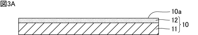
- FIG. 3A is a cross-sectional view that illustrates an example of a step of forming an insulating layer in the first embodiment.
- FIG. 3B is a cross-sectional view that illustrates an example of a step of forming a lower electrode in the first embodiment.
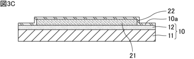
- FIG. 3C is a cross-sectional view that illustrates an example of a step of forming a dielectric film in the first embodiment.
- FIG. 1 is a plan view illustrating an example of a capacitor according to a first embodiment of the present invention.
- FIG. 2 is an example of a cross-sectional view of the capacitor shown in FIG. 1 taken along line AA.
- FIG. 3A is a cross-sectional view that illustrates an example of a step of forming an insulating layer
- FIG. 3D is a cross-sectional view that illustrates an example of a step of forming a metal film for an upper electrode in the first embodiment.
- FIG. 3E is a cross-sectional view that illustrates an example of a first step of processing a metal film for an upper electrode in the first embodiment.
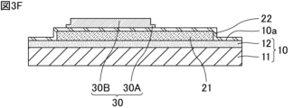
- FIG. 3F is a cross-sectional view that illustrates an example of a second step of processing the metal film for the upper electrode in the first embodiment.
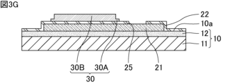
- FIG. 3G is a cross-sectional view that illustrates an example of a step of forming a via in the dielectric film in the first embodiment.
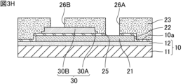
- FIG. 3H is a cross-sectional view that illustrates an example of a step of forming a protective layer in the first embodiment.
- FIG. 3I is a cross-sectional view that illustrates an example of a step of forming external electrodes in the first embodiment.
- FIG. 4 is a cross-sectional view illustrating an example of a capacitor according to the second embodiment of the present invention.
- FIG. 5A is a cross-sectional view that illustrates an example of a step of forming an insulating layer in the second embodiment.
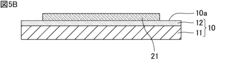
- FIG. 5B is a cross-sectional view that illustrates an example of a step of forming a lower electrode in the second embodiment.
- FIG. 5C is a cross-sectional view that illustrates an example of a step of forming a dielectric film in the second embodiment.
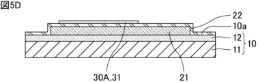
- FIG. 5D is a cross-sectional view that illustrates an example of a step of forming a lower layer of the upper electrode in the second embodiment.
- FIG. 5E is a cross-sectional view that illustrates an example of a step of forming an upper layer of the upper electrode in the second embodiment.
- FIG. 5F is a cross-sectional view that illustrates an example of a step of forming a via in the dielectric film in the second embodiment.
- FIG. 5G is a cross-sectional view that illustrates an example of a step of forming a protective layer in the second embodiment.
- FIG. 5H is a cross-sectional view that illustrates an example of a step of forming external electrodes in the second embodiment.
- FIG. 6 is a cross-sectional view illustrating an example of a capacitor according to the third embodiment of the present invention.
- FIG. 7A is a cross-sectional view illustrating an example of a step of forming an insulating layer in the third embodiment.
- FIG. 7B is a cross-sectional view that illustrates an example of a step of forming a lower electrode in the third embodiment.
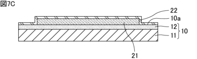
- FIG. 7C is a cross-sectional view illustrating an example of a step of forming a dielectric film in the third embodiment.
- FIG. 7D is a cross-sectional view that illustrates an example of a step of forming a lower layer of the upper electrode in the third embodiment.
- FIG. 7A is a cross-sectional view illustrating an example of a step of forming an insulating layer in the third embodiment.
- FIG. 7B is a cross-sectional view that illustrates an example of a step of forming a lower electrode in the third embodiment.
- FIG. 7C is a cross-
- FIG. 7E is a cross-sectional view illustrating an example of a step of forming an upper layer of the upper electrode in the third embodiment.
- FIG. 7F is a cross-sectional view that illustrates an example of a step of forming a via in the dielectric film in the third embodiment.
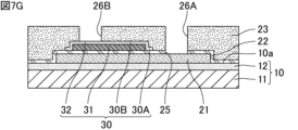
- FIG. 7G is a cross-sectional view that illustrates an example of a step of forming a protective layer in the third embodiment.
- FIG. 7H is a cross-sectional view that illustrates an example of a step of forming external electrodes in the third embodiment.
- FIG. 8 is a cross-sectional view illustrating an example of a capacitor according to the fourth embodiment of the present invention.
- FIG. 8 is a cross-sectional view illustrating an example of a capacitor according to the fourth embodiment of the present invention.
- FIG. 9A is a cross-sectional view illustrating an example of a step of forming an insulating layer in the fourth embodiment.
- FIG. 9B is a cross-sectional view that illustrates an example of a step of forming a lower electrode in the fourth embodiment.
- FIG. 9C is a cross-sectional view illustrating an example of a step of forming a dielectric film in the fourth embodiment.
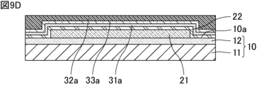
- FIG. 9D is a cross-sectional view that illustrates an example of a step of forming a metal film for an upper electrode in the fourth embodiment.
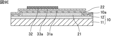
- FIG. 9E is a cross-sectional view illustrating an example of a first process of processing a metal film for an upper electrode in the fourth embodiment.
- FIG. 9F is a cross-sectional view illustrating an example of a second process of processing the metal film for the upper electrode in the fourth embodiment.
- FIG. 9G is a cross-sectional view illustrating an example of a third process of processing the metal film for the upper electrode in the fourth embodiment.
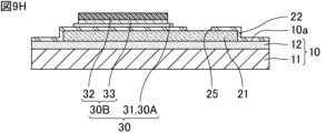
- FIG. 9H is a cross-sectional view that illustrates an example of a step of forming a via in the dielectric film in the fourth embodiment.
- FIG. 9I is a cross-sectional view that illustrates an example of a step of forming a protective layer in the fourth embodiment.
- FIG. 9J is a cross-sectional view illustrating a schematic example of a step of forming external electrodes in the fourth embodiment.
- FIG. 10 is a cross-sectional view illustrating an example of a capacitor according to the fifth embodiment of the present invention.
- the present invention is not limited to the following configurations, and can be modified and applied as appropriate within the scope of the present invention. Note that the present invention also includes a combination of two or more of the individual desirable configurations described below.
- each embodiment will be referred to simply as the "semiconductor device of the present invention.”
- the shape and arrangement of each component of the semiconductor device of the present invention are not limited to the examples shown in the drawings.
- the semiconductor device of the present invention may be a capacitor itself, or may be a device that includes a capacitor.
- FIG. 1 is a plan view showing an example of the capacitor according to embodiment 1 of the present invention.
- Fig. 2 is an example of a cross-sectional view taken along line AA of the capacitor shown in Fig. 1.
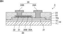
- the capacitor 1 shown in Figures 1 and 2 comprises a substrate 10 having an insulating surface (main surface) 10a, a lower electrode 21 provided on the insulating surface 10a, a dielectric film 22 provided on the lower electrode 21, and an upper electrode 30 provided on the dielectric film 22.
- the substrate 10 has a semiconductor substrate 11 and an insulating layer 12 provided on the semiconductor substrate 11, but if the substrate 10 is an insulating substrate such as glass or alumina, the insulating layer 12 can be omitted.
- the capacitor 1 further includes a protective layer 23 provided on the dielectric film 22 and the upper electrode 30, and an external electrode 24 that penetrates the protective layer 23.
- the external electrode 24 includes a first external electrode 24A connected to the lower electrode 21 and a second external electrode 24B connected to the upper electrode 30.
- the first external electrode 24A penetrates the protective layer 23 and the dielectric film 22, and the second external electrode 24B penetrates the protective layer 23.
- the capacitor 1 may further include a moisture-resistant film (not shown) provided on the dielectric film 22 and the upper electrode 30.
- the lower electrode 21, the dielectric film 22, and the upper electrode 30 are stacked in this order to form an MIM capacitor structure.
- charge can be stored in the dielectric film 22.
- the term "convex shape” refers to a shape having a lower portion and an upper portion disposed on the lower portion, where the entire upper portion is inside the lower portion in a plan view. Therefore, the end face of the upper portion is not particularly limited to a flat surface such as a vertical surface (see FIG. 2), but may be an uneven surface, and for example, the end of the upper portion may be in an overhanging shape (see FIG. 10 described below).
- the substrate 10, the lower electrode 21, and the upper electrode 30 are all rectangular.
- the lower electrode 21 is formed within the region of the substrate 10, and in a plan view, the upper electrode 30 is formed within the formation region of the lower electrode 21.
- the lower portion 30A and the upper portion 30B of the upper electrode 30 are both rectangular.
- the upper portion 30B is formed within the formation area of the lower portion 30A. That is, in plan view, the lower portion 30A protrudes from the upper portion 30B in a frame shape around the entire periphery of the upper portion 30B.
- the lower portion 30A is composed of a fringe portion (brim-shaped portion) that protrudes from the upper portion 30B around the entire periphery and a central portion that is located at the same height as the fringe portion, and the upper portion 30B corresponds to the portion of the upper electrode 30 excluding the lower portion 30A.
- the upper electrode 30 is composed of a single layer.
- the upper portion 30B of the upper electrode 30 and the lower portion 30A of the upper electrode 30 are composed of the same material, and there is no boundary between them. This makes it possible to prevent the capacitor 1 from being adversely affected by any such boundary.
- the thickness of the lower portion 30A of the upper electrode 30 is preferably smaller than the thickness of the upper portion 30B of the upper electrode 30. This effectively reduces ESR and capacitance variations.
- the thickness of the upper portion 30B is preferably 1 ⁇ m or more. This allows the ESR to be further reduced.
- the thickness of the upper portion 30B is more preferably 1 ⁇ m or more and 5 ⁇ m or less, and even more preferably 3 ⁇ m or more and 5 ⁇ m or less.
- the thickness of the upper portion 30B may be the thickness of the portion located above the fringe portion of the lower portion 30A.
- FIG. 3A is a cross-sectional view showing an example of a process for forming an insulating layer in embodiment 1.
- FIG. 3B is a cross-sectional view showing an example of a process for forming a lower electrode in embodiment 1.
- FIG. 3C is a cross-sectional view showing an example of a process for forming a dielectric film in embodiment 1.
- FIG. 3D is a cross-sectional view showing an example of a process for forming a metal film for an upper electrode in embodiment 1.
- FIG. 3E is a cross-sectional view showing an example of a first process for processing a metal film for an upper electrode in embodiment 1.
- FIG. 3F is a cross-sectional view showing an example of a second process for processing a metal film for an upper electrode in embodiment 1.
- 3G is a cross-sectional view showing an example of a process for forming a via in a dielectric film in embodiment 1.
- FIG. 3H is a cross-sectional view showing an example of a process for forming a protective layer in embodiment 1.
- FIG. 3I is a cross-sectional view showing an example of a process for forming an external electrode in embodiment 1.
- FIG. 3A to 3I focus on one capacitor, multiple capacitors may be formed on a substrate at the same time. That is, an aggregate substrate having multiple capacitors may be manufactured and then singulated into individual capacitors. The same applies to the second and subsequent embodiments.
- an insulating layer 12 made of SiO2 , SiN, Al2O3 , or the like is formed on a semiconductor substrate 11 such as a silicon substrate or a gallium arsenide substrate by a CVD (Chemical Vapor Deposition) method, a PVD (Physical Vapor Deposition) method, or the like.
- a substrate 10 having an insulating surface 10a is an insulating substrate such as glass or alumina, the insulating layer 12 can be omitted.
- a lower electrode 21 is formed on the insulating surface 10a (insulating layer 12) by a lift-off method, a plating method, an etching method, or the like.
- the material of the lower electrode 21 is preferably Cu, Ag, Au, Al, Pt, or an alloy containing at least one of these metals.
- a resist pattern for the upper portion 30B of the upper electrode 30 is formed by photolithography, and the metal film 30a is processed by etching.
- the etching time, etc. is adjusted so that a thin film remains.
- a resist pattern for the lower portion 30A of the upper electrode 30 is formed by photolithography, and the lower portion 30A is formed by etching. At this time, it is preferable to use a method such as dry etching, which has high processing accuracy.
- the aggregate substrate When manufacturing an aggregate substrate having multiple capacitors, the aggregate substrate is thinned to the desired element thickness by back grinding, and then separated into individual pieces by blade dicing, stealth dicing, plasma dicing, etc. In other words, the aggregate substrate is cut into pieces the size of individual capacitors.
- Embodiment 2 This embodiment differs from the first embodiment in that the upper electrode is formed of a plurality of layers, two layers in this embodiment.
- FIG. 4 is a cross-sectional view showing a schematic example of a capacitor according to embodiment 2 of the present invention. Note that FIG. 4 corresponds to the cross-sectional view of the capacitor shown in FIG. 1 taken along line A-A.
- the upper electrode 30 has a lower layer 31 and an upper layer 32 provided on the lower layer 31. This allows the convex structure of the upper electrode 30 to be formed from different materials, so that by combining a material that is easy to process with a material that has low resistance, the ESR can be further reduced and the capacitance variation can be made smaller. Also, compared to embodiment 1, it is easier to control the film thickness of the lower portion 30A (lower layer 31) of the upper electrode 30.
- the lower layer 31 corresponds to the lower portion 30A of the upper electrode 30
- the upper layer 32 corresponds to the upper portion 30B of the upper electrode 30.
- the upper layer 32 and the lower layer 31 may contain the same material, and the material constituting the upper layer 32 may be the same as the material constituting the lower layer 31. This can prevent a boundary from being formed between the upper layer 32 and the lower layer 31. Therefore, it is possible to prevent the capacitor 2 from being adversely affected by such a boundary.
- FIG. 5A is a cross-sectional view showing an example of a process for forming an insulating layer in embodiment 2.
- FIG. 5B is a cross-sectional view showing an example of a process for forming a lower electrode in embodiment 2.
- FIG. 5C is a cross-sectional view showing an example of a process for forming a dielectric film in embodiment 2.
- FIG. 5D is a cross-sectional view showing an example of a process for forming a lower layer of an upper electrode in embodiment 2.
- FIG. 5E is a cross-sectional view showing an example of a process for forming an upper layer of an upper electrode in embodiment 2.
- FIG. 5F is a cross-sectional view showing an example of a process for forming a via in a dielectric film in embodiment 2.
- FIG. 5G is a cross-sectional view showing an example of a process for forming a protective layer in embodiment 2.
- FIG. 5H is a cross-sectional view showing an example of a process for forming an
- the lower layer 31 of the upper electrode 30 is formed on the dielectric film 22.
- the material of the lower layer 31 is preferably Cu, Ag, Au, Al, Pt, or an alloy containing at least one of these metals. At this time, it is preferable to use a method such as dry etching, which has high processing accuracy.
- the lower layer 31 corresponds to the lower portion 30A of the upper electrode 30
- the upper layer 32 corresponds to the upper portion 30B of the upper electrode 30.
- the end of the upper layer 32 is in an overhanging shape.
- the width w of the insulating film 27 overlapping with the upper layer 32 is not particularly limited, but is preferably 1% or more and 50% or less of the width W of the upper layer 32, and more preferably 1% or more and 10% or less.
- the percentage of width w relative to width W shall be calculated based on widths w and W measured at the same cross section.
- the semiconductor device of the present invention is not limited to the above-described embodiment, and various applications and modifications can be made within the scope of the present invention with respect to the configuration and manufacturing conditions of the semiconductor device such as a capacitor.
- ⁇ 5> The semiconductor device according to ⁇ 3>, wherein the upper electrode has a metal layer provided between the upper layer and the lower layer.
- ⁇ 6> The semiconductor device according to ⁇ 3>, further comprising an insulating film provided between an end of the upper layer and an end of the lower layer.
- ⁇ 7> The semiconductor device according to any one of ⁇ 2> to ⁇ 6>, wherein the upper layer and the lower layer contain the same material.
Landscapes
- Engineering & Computer Science (AREA)
- Power Engineering (AREA)
- Microelectronics & Electronic Packaging (AREA)
- Manufacturing & Machinery (AREA)
- Semiconductor Integrated Circuits (AREA)
Priority Applications (3)
| Application Number | Priority Date | Filing Date | Title |
|---|---|---|---|
| CN202480033619.4A CN121264190A (zh) | 2023-06-07 | 2024-05-15 | 半导体装置 |
| JP2025526022A JPWO2024252871A1 (https=) | 2023-06-07 | 2024-05-15 | |
| US19/401,766 US20260113960A1 (en) | 2023-06-07 | 2025-11-26 | Semiconductor device |
Applications Claiming Priority (2)
| Application Number | Priority Date | Filing Date | Title |
|---|---|---|---|
| JP2023-094200 | 2023-06-07 | ||
| JP2023094200 | 2023-06-07 |
Related Child Applications (1)
| Application Number | Title | Priority Date | Filing Date |
|---|---|---|---|
| US19/401,766 Continuation US20260113960A1 (en) | 2023-06-07 | 2025-11-26 | Semiconductor device |
Publications (1)
| Publication Number | Publication Date |
|---|---|
| WO2024252871A1 true WO2024252871A1 (ja) | 2024-12-12 |
Family
ID=93795300
Family Applications (1)
| Application Number | Title | Priority Date | Filing Date |
|---|---|---|---|
| PCT/JP2024/017951 Ceased WO2024252871A1 (ja) | 2023-06-07 | 2024-05-15 | 半導体装置 |
Country Status (4)
| Country | Link |
|---|---|
| US (1) | US20260113960A1 (https=) |
| JP (1) | JPWO2024252871A1 (https=) |
| CN (1) | CN121264190A (https=) |
| WO (1) | WO2024252871A1 (https=) |
Citations (4)
| Publication number | Priority date | Publication date | Assignee | Title |
|---|---|---|---|---|
| JP2004327867A (ja) * | 2003-04-25 | 2004-11-18 | Kyocera Corp | 薄膜コンデンサおよびそれを用いたコンデンサ基板 |
| JP2012151220A (ja) * | 2011-01-18 | 2012-08-09 | Asahi Kasei Electronics Co Ltd | 容量素子及びその製造方法並びに半導体集積回路 |
| WO2018008625A1 (ja) * | 2016-07-07 | 2018-01-11 | 株式会社村田製作所 | キャパシタ |
| WO2022239722A1 (ja) * | 2021-05-10 | 2022-11-17 | 株式会社村田製作所 | 半導体装置、マッチング回路及びフィルタ回路 |
-
2024
- 2024-05-15 CN CN202480033619.4A patent/CN121264190A/zh active Pending
- 2024-05-15 JP JP2025526022A patent/JPWO2024252871A1/ja active Pending
- 2024-05-15 WO PCT/JP2024/017951 patent/WO2024252871A1/ja not_active Ceased
-
2025
- 2025-11-26 US US19/401,766 patent/US20260113960A1/en active Pending
Patent Citations (4)
| Publication number | Priority date | Publication date | Assignee | Title |
|---|---|---|---|---|
| JP2004327867A (ja) * | 2003-04-25 | 2004-11-18 | Kyocera Corp | 薄膜コンデンサおよびそれを用いたコンデンサ基板 |
| JP2012151220A (ja) * | 2011-01-18 | 2012-08-09 | Asahi Kasei Electronics Co Ltd | 容量素子及びその製造方法並びに半導体集積回路 |
| WO2018008625A1 (ja) * | 2016-07-07 | 2018-01-11 | 株式会社村田製作所 | キャパシタ |
| WO2022239722A1 (ja) * | 2021-05-10 | 2022-11-17 | 株式会社村田製作所 | 半導体装置、マッチング回路及びフィルタ回路 |
Also Published As
| Publication number | Publication date |
|---|---|
| US20260113960A1 (en) | 2026-04-23 |
| JPWO2024252871A1 (https=) | 2024-12-12 |
| CN121264190A (zh) | 2026-01-02 |
Similar Documents
| Publication | Publication Date | Title |
|---|---|---|
| JP6856095B2 (ja) | キャパシタ | |
| JP2020115587A (ja) | キャパシタ | |
| JP6372640B2 (ja) | キャパシタ | |
| JP7197001B2 (ja) | キャパシタ | |
| US9620581B2 (en) | Multilayer electrical device | |
| US11476055B2 (en) | Thin film capacitor and method of manufacturing the same | |
| US20070065994A1 (en) | Passivation Structure for Ferroelectric Thin-Film Devices | |
| JP6788847B2 (ja) | キャパシタ | |
| TWI290726B (en) | Method of manufacturing passive devices on a semiconductor substrate | |
| JP7439392B2 (ja) | キャパシタ | |
| JP6819894B2 (ja) | 電子部品 | |
| WO2024252871A1 (ja) | 半導体装置 | |
| WO2022239722A1 (ja) | 半導体装置、マッチング回路及びフィルタ回路 | |
| JP7156369B2 (ja) | キャパシタ集合体 | |
| JP5929540B2 (ja) | 電子部品 | |
| JP6079279B2 (ja) | 半導体装置、半導体装置の製造方法 | |
| JP7484903B2 (ja) | キャパシタ | |
| US20260075852A1 (en) | Semiconductor device and method for fabricating the same | |
| JP7609264B2 (ja) | 半導体装置 | |
| WO2025263313A1 (ja) | 受動電子部品 | |
| WO2025120916A1 (ja) | 電子部品及びその製造方法 | |
| WO2025263314A1 (ja) | 受動電子部品及び受動電子部品の製造方法 | |
| TW202612147A (zh) | 半導體元件及其製作方法 | |
| JP2003045746A (ja) | 薄膜コンデンサ |
Legal Events
| Date | Code | Title | Description |
|---|---|---|---|
| 121 | Ep: the epo has been informed by wipo that ep was designated in this application |
Ref document number: 24819108 Country of ref document: EP Kind code of ref document: A1 |
|
| ENP | Entry into the national phase |
Ref document number: 2025526022 Country of ref document: JP Kind code of ref document: A |
|
| WWE | Wipo information: entry into national phase |
Ref document number: 2025526022 Country of ref document: JP |
|
| NENP | Non-entry into the national phase |
Ref country code: DE |