WO2024252830A1 - 半導体装置および車両 - Google Patents
半導体装置および車両 Download PDFInfo
- Publication number
- WO2024252830A1 WO2024252830A1 PCT/JP2024/016981 JP2024016981W WO2024252830A1 WO 2024252830 A1 WO2024252830 A1 WO 2024252830A1 JP 2024016981 W JP2024016981 W JP 2024016981W WO 2024252830 A1 WO2024252830 A1 WO 2024252830A1
- Authority
- WO
- WIPO (PCT)
- Prior art keywords
- terminal
- semiconductor device
- lead
- tip
- thickness direction
- Prior art date
- Legal status (The legal status is an assumption and is not a legal conclusion. Google has not performed a legal analysis and makes no representation as to the accuracy of the status listed.)
- Ceased
Links
Images















Classifications
-
- H—ELECTRICITY
- H10—SEMICONDUCTOR DEVICES; ELECTRIC SOLID-STATE DEVICES NOT OTHERWISE PROVIDED FOR
- H10W—GENERIC PACKAGES, INTERCONNECTIONS, CONNECTORS OR OTHER CONSTRUCTIONAL DETAILS OF DEVICES COVERED BY CLASS H10
- H10W70/00—Package substrates; Interposers; Redistribution layers [RDL]
- H10W70/40—Leadframes
- H10W70/421—Shapes or dispositions
- H10W70/424—Cross-sectional shapes
- H10W70/427—Bent parts
- H10W70/429—Bent parts being the outer leads
-
- H—ELECTRICITY
- H10—SEMICONDUCTOR DEVICES; ELECTRIC SOLID-STATE DEVICES NOT OTHERWISE PROVIDED FOR
- H10W—GENERIC PACKAGES, INTERCONNECTIONS, CONNECTORS OR OTHER CONSTRUCTIONAL DETAILS OF DEVICES COVERED BY CLASS H10
- H10W72/00—Interconnections or connectors in packages
-
- H—ELECTRICITY
- H10—SEMICONDUCTOR DEVICES; ELECTRIC SOLID-STATE DEVICES NOT OTHERWISE PROVIDED FOR
- H10W—GENERIC PACKAGES, INTERCONNECTIONS, CONNECTORS OR OTHER CONSTRUCTIONAL DETAILS OF DEVICES COVERED BY CLASS H10
- H10W70/00—Package substrates; Interposers; Redistribution layers [RDL]
- H10W70/40—Leadframes
- H10W70/474—Batteries in combination with leadframes
-
- H—ELECTRICITY
- H10—SEMICONDUCTOR DEVICES; ELECTRIC SOLID-STATE DEVICES NOT OTHERWISE PROVIDED FOR
- H10W—GENERIC PACKAGES, INTERCONNECTIONS, CONNECTORS OR OTHER CONSTRUCTIONAL DETAILS OF DEVICES COVERED BY CLASS H10
- H10W72/00—Interconnections or connectors in packages
- H10W72/851—Dispositions of multiple connectors or interconnections
- H10W72/853—On the same surface
- H10W72/868—Die-attach connectors and strap connectors
-
- H—ELECTRICITY
- H10—SEMICONDUCTOR DEVICES; ELECTRIC SOLID-STATE DEVICES NOT OTHERWISE PROVIDED FOR
- H10W—GENERIC PACKAGES, INTERCONNECTIONS, CONNECTORS OR OTHER CONSTRUCTIONAL DETAILS OF DEVICES COVERED BY CLASS H10
- H10W74/00—Encapsulations, e.g. protective coatings
- H10W74/10—Encapsulations, e.g. protective coatings characterised by their shape or disposition
- H10W74/111—Encapsulations, e.g. protective coatings characterised by their shape or disposition the semiconductor body being completely enclosed
- H10W74/114—Encapsulations, e.g. protective coatings characterised by their shape or disposition the semiconductor body being completely enclosed by a substrate and the encapsulations
-
- H—ELECTRICITY
- H10—SEMICONDUCTOR DEVICES; ELECTRIC SOLID-STATE DEVICES NOT OTHERWISE PROVIDED FOR
- H10W—GENERIC PACKAGES, INTERCONNECTIONS, CONNECTORS OR OTHER CONSTRUCTIONAL DETAILS OF DEVICES COVERED BY CLASS H10
- H10W90/00—Package configurations
- H10W90/701—Package configurations characterised by the relative positions of pads or connectors relative to package parts
- H10W90/751—Package configurations characterised by the relative positions of pads or connectors relative to package parts of bond wires
- H10W90/756—Package configurations characterised by the relative positions of pads or connectors relative to package parts of bond wires between a chip and a stacked lead frame, conducting package substrate or heat sink
-
- H—ELECTRICITY
- H10—SEMICONDUCTOR DEVICES; ELECTRIC SOLID-STATE DEVICES NOT OTHERWISE PROVIDED FOR
- H10W—GENERIC PACKAGES, INTERCONNECTIONS, CONNECTORS OR OTHER CONSTRUCTIONAL DETAILS OF DEVICES COVERED BY CLASS H10
- H10W90/00—Package configurations
- H10W90/701—Package configurations characterised by the relative positions of pads or connectors relative to package parts
- H10W90/761—Package configurations characterised by the relative positions of pads or connectors relative to package parts of strap connectors
- H10W90/766—Package configurations characterised by the relative positions of pads or connectors relative to package parts of strap connectors between a chip and a stacked lead frame, conducting package substrate or heat sink
Definitions
- This disclosure relates to a semiconductor device and a vehicle.
- Patent Document 1 discloses an example of a semiconductor device.
- the semiconductor device described in Patent Document 1 comprises a first lead including a first pad having a main pad surface and a back pad surface, a second lead, a third lead, a semiconductor element mounted on the main pad surface, and a sealing resin in contact with the main pad surface and covering the semiconductor element.
- the first lead, the second lead, and the third lead have a first terminal, a second terminal, and a third terminal extending in the same direction.
- the first terminal, the second terminal, and the third terminal are inserted into through holes in a circuit board or the like, thereby mounting the semiconductor device on the circuit board.
- a heat sink for example, an insulating sheet is provided between the back pad surface and the heat sink.
- semiconductor devices may also be required to be surface-mounted on the circuit board.
- An object of the present disclosure is to provide a semiconductor device that is an improvement over conventional semiconductor devices.
- an object of the present disclosure is to provide a semiconductor device that can be surface mounted.
- Another object of the present disclosure is to provide a vehicle equipped with a semiconductor device that can be surface mounted.
- the semiconductor device provided by the first aspect of the present disclosure includes a semiconductor element, a die pad portion having a first lead main surface facing one side of the thickness direction and on which the semiconductor element is mounted, and a first lead back surface facing the other side of the thickness direction, a first terminal portion, and a sealing resin having a first resin surface facing one side of the thickness direction, a second resin surface facing the other side of the thickness direction, and a third resin surface facing one side of a first direction perpendicular to the thickness direction, and covering the semiconductor element and a part of the die pad portion.
- the first lead includes a metal layer covering a part of the first terminal portion.
- the first lead back surface is exposed from the second resin surface.
- the first terminal portion has a first terminal root portion and at least one first terminal tip portion.
- the first terminal root portion penetrates the third resin surface and is separated from the first resin surface in the thickness direction.
- the at least one first terminal tip portion is located on the one side of the thickness direction from the first terminal root portion and is used for mounting.
- the at least one first terminal tip portion has a first tip surface and a concave surface connected to the first tip surface. The first tip surface is exposed from the metal layer, and the concave surface is covered by the metal layer.
- the vehicle provided by the second aspect of the present disclosure includes a drive source, a storage battery that stores power to be supplied to the drive source, and an on-board charger that converts power input from the outside and supplies it to the storage battery.
- the on-board charger includes the semiconductor device provided by the first aspect.
- the above configuration makes it possible to provide a surface-mountable semiconductor device and a vehicle equipped with a surface-mountable semiconductor device.
- FIG. 1 is a perspective view showing a semiconductor device according to a first embodiment.
- FIG. 2 is a perspective view of FIG. 1 in which the sealing resin is shown by imaginary lines and a number of connecting members are omitted.
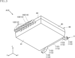
- FIG. 3 is a perspective view showing the semiconductor device according to the first embodiment.
- FIG. 4 is a perspective view of FIG. 3 in which the sealing resin is shown by imaginary lines.
- FIG. 5 is a perspective view showing the semiconductor device according to the first embodiment.
- FIG. 6 is a plan view showing the semiconductor device according to the first embodiment.
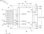
- FIG. 7 is a diagram showing the sealing resin by imaginary lines in the plan view of FIG.
- FIG. 8 is a bottom view showing the semiconductor device according to the first embodiment.
- FIG. 9 is a bottom view of FIG.
- FIG. 10 is a front view showing the semiconductor device according to the first embodiment.
- FIG. 11 is a right side view showing the semiconductor device according to the first embodiment.
- FIG. 12 is a cross-sectional view taken along line XII-XII in FIG.
- FIG. 13 is a cross-sectional view taken along line XIII-XIII in FIG.
- FIG. 14 is a cross-sectional view taken along line XIV-XIV in FIG.
- FIG. 15 is a cross-sectional view taken along line XV-XV in FIG.
- FIG. 16 is an enlarged perspective view of a main portion (a tip end portion of the first terminal) of FIG.
- FIG. 10 is a front view showing the semiconductor device according to the first embodiment.
- FIG. 11 is a right side view showing the semiconductor device according to the first embodiment.
- FIG. 12 is a cross-sectional view taken along line XII-XII in FIG.
- FIG. 13 is a cross-sectional view taken along line
- FIG. 17 is an enlarged bottom view of a main portion (a tip portion of the first terminal) of FIG. 8.
- FIG. FIG. 18 is an enlarged front view of a main portion (a tip portion of the first terminal) of FIG.
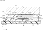
- FIG. 19 is a cross-sectional view showing a state in which the semiconductor device according to the first embodiment is used.
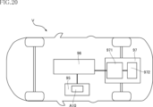
- FIG. 20 is a schematic diagram showing a vehicle including the semiconductor device according to the first embodiment.
- FIG. 21 is a bottom view showing a step of the method for manufacturing the semiconductor device according to the first embodiment.
- FIG. 22 is a perspective view showing a semiconductor device according to the second embodiment and corresponds to FIG.
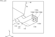
- FIG. 23 is an enlarged perspective view of a main portion (a tip portion of the first terminal) of FIG. 22, and corresponds to FIG.
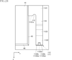
- FIG. 24 is a bottom view of a main part of the semiconductor device according to the second embodiment, and corresponds to FIG. 17.
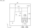
- FIG. 25 is a main part front view showing the semiconductor device according to the second embodiment, and corresponds to FIG.
- FIG. 26 is a perspective view showing a semiconductor device according to the third embodiment, and corresponds to FIG.
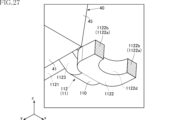
- FIG. 27 is an enlarged perspective view of a main portion (a tip portion of the first terminal) of FIG. 26, and corresponds to FIG.
- FIG. 28 is a bottom view of a main portion showing the semiconductor device according to the third embodiment, and corresponds to FIG. 17.
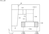
- FIG. 29 is a main part front view showing the semiconductor device according to the third embodiment, and corresponds to FIG. FIG.
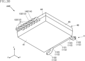
- FIG. 30 is a perspective view showing a semiconductor device according to the fourth embodiment and corresponds to FIG.
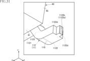
- FIG. 31 is an enlarged perspective view of a main portion (a tip portion of the first terminal) of FIG. 30, and corresponds to FIG.
- FIG. 32 is a bottom view of a main portion showing the semiconductor device according to the fourth embodiment, and corresponds to FIG.
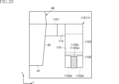
- FIG. 33 is a main part front view showing the semiconductor device according to the fourth embodiment, and corresponds to FIG.
- FIG. 34 is a perspective view showing a semiconductor device according to the fifth embodiment and corresponds to FIG.
- FIG. 35 is a perspective view showing a semiconductor device according to a modification of the fifth embodiment, and corresponds to FIG. FIG.
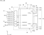
- FIG. 36 is a plan view showing a semiconductor device according to a first modification, in which a sealing resin is indicated by imaginary lines.
- FIG. 37 is a plan view showing a semiconductor device according to a second modification, in which a sealing resin is indicated by imaginary lines.
- 38 is a bottom view showing a step of the method for manufacturing the semiconductor device shown in FIG. 37, and corresponds to FIG. 21.
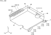
- FIG. FIG. 39 is a perspective view showing a semiconductor device according to a third modified example, and corresponds to FIG.
- FIG. 40 is a perspective view showing a semiconductor device according to a third modified example, and corresponds to FIG.
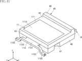
- FIG. 41 is a perspective view showing a semiconductor device according to a fourth modified example, and corresponds to FIG.
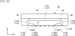
- FIG. 42 is a right side view showing a semiconductor device according to a fifth modified example, and corresponds to FIG.
- an object A is formed on an object B
- an object A is formed on (an object B)
- an object A is formed directly on an object B
- an object A is formed on an object B with another object interposed between the object A and the object B” unless otherwise specified.
- an object A is disposed on an object B” and “an object A is disposed on (an object B)” include “an object A is disposed directly on an object B” and “an object A is disposed on (an object B) with another object interposed between the object A and the object B” unless otherwise specified.
- an object A is located on (an object B) includes “an object A is in contact with an object B and is located on (an object B)” and “an object A is located on (an object B) with another object interposed between the object A and the object B".
- an object A overlaps an object B includes “an object A overlaps the entire object B” and “an object A overlaps a part of an object B” unless otherwise specified.
- An object A (its material) contains a certain material C includes “an object A (its material) is made of a certain material C” and “an object A (its material) is mainly composed of a certain material C.”
- a certain surface A faces a certain direction B (one side or the other side of a certain surface B) includes, unless otherwise specified, not limited to the case where the angle of surface A with respect to direction B is 90°, and includes the case where surface A is inclined with respect to direction B.
- a certain surface A is perpendicular to a certain surface B includes, unless otherwise specified, not limited to the case where the angle of surface A with respect to surface B is 90°, and includes the case where surface A is inclined with respect to surface B.
- First embodiment: 1 to 18 show a semiconductor device A10 according to a first embodiment.
- the semiconductor device A10 includes a conductive member 10, a semiconductor element 20, a plurality of connecting members 31, 32, and 33, and a sealing resin 40.
- the thickness direction of the semiconductor device A10 is referred to as the "thickness direction z".
- one side of the thickness direction z may be referred to as the lower side, and the other side as the upper side.
- the terms “upper”, “lower”, “upper”, “lower”, “top surface” and “bottom surface” indicate the relative positional relationship of each component, etc. in the thickness direction z, and do not necessarily define the relationship with the direction of gravity.
- One direction perpendicular to the thickness direction z is referred to as the "first direction x”.
- the direction perpendicular to the thickness direction z and the first direction x is referred to as the "second direction y”.
- the conductive member 10 is a member that constitutes a conductive path to the semiconductor element 20.
- the conductive member 10 of this embodiment includes a first lead 11, a second lead 12, a third lead 13, and a fourth lead 14.
- the material of the first lead 11, the second lead 12, the third lead 13, and the fourth lead 14 is not limited in any way and includes, for example, copper (Cu) or a copper alloy.
- the first lead 11, the second lead 12, the third lead 13, and the fourth lead 14 are plated in appropriate locations with silver (Ag), nickel (Ni), tin (Sn), or the like.
- the plating corresponds to each of the metal layers 110, 120, 130, and 140, which will be described in detail later. In Figures 1 to 11, the plating (each of the metal layers 110, 120, 130, and 140, which will be described later) is omitted from illustration.
- the first lead 11 includes a metal layer 110, a die pad portion 111, and a first terminal portion 112.
- the metal layer 110 covers a portion of the first lead 11.
- the metal layer 110 is a plating of silver (Ag), nickel (Ni), tin (Sn), or the like.
- the material of the metal layer 110 is not limited to these, but it is preferable that the material has a higher bonding strength with the bonding layer 29 described below than the material of the first lead 11 (e.g., Cu).
- the die pad portion 111 has a first lead main surface 1111 and a first lead back surface 1112.
- the first lead main surface 1111 is a surface facing one side (downward) in the thickness direction z.
- the first lead back surface 1112 is a surface facing the other side (upward) in the thickness direction z.
- a semiconductor element 20 is mounted on the first lead main surface 1111.
- the die pad portion 111 of this embodiment further has a first lead side surface 1113 and a first intermediate surface 1114.
- the first lead side surface 1113 is located between the first lead main surface 1111 and the first lead back surface 1112 in the thickness direction z, and is a surface that faces downward in the first direction x.
- the first intermediate surface 1114 is located between the first lead main surface 1111 and the first lead back surface 1112 in the thickness direction z, and is a surface that faces downward in the thickness direction z (the same side as the first lead main surface 1111).
- the shape of the die pad portion 111 is not limited in any way. In the illustrated example, the die pad portion 111 is rectangular when viewed in the thickness direction z.
- the shapes of the first lead main surface 1111 and the first lead back surface 1112 are not limited in any way, and in the illustrated example, they are rectangular when viewed in the thickness direction z.
- the entire surface of the die pad portion 111 is covered with a metal layer 110.
- the metal layer 110 does not have to be formed in the area where the semiconductor element 20 is bonded (the area in contact with the bonding layer 29 described below), and may be made of a different material from that in other areas.
- the first terminal portion 112 is connected to the die pad portion 111. Most of the first terminal portion 112 is exposed from the sealing resin 40. The first terminal portion 112 protrudes to one side in the first direction x relative to the sealing resin 40. The first terminal portion 112 is bent in a gull-wing shape. The first terminal portion 112 has a first terminal root portion 1121, two first terminal tip portions 1122, and two first terminal middle portions 1123.
- the first terminal root portion 1121 is connected to the die pad portion 111, extends from the die pad portion 111 in one direction in the first direction x, and is parallel to a plane (x-y plane) perpendicular to the thickness direction z in the illustrated example.
- the thickness (dimension along the thickness direction z) of the die pad portion 111 is greater than the thickness (dimension along the thickness direction z) of the first terminal root portion 1121.
- the first terminal portion 112 in this embodiment has one first terminal root portion 1121.
- the shape of the first terminal root portion 1121 is not limited in any way, and in the illustrated example, it is rectangular when viewed in the thickness direction z.
- the first terminal root portion 1121 is separated from the first lead back surface 1112 in the thickness direction z, and in the illustrated example, is in contact with the first lead main surface 1111.
- the bottom surface of the first terminal base portion 1121 (the surface facing downward in the thickness direction z) is flush with the first lead main surface 1111.
- a portion of the surface of the first terminal base portion 1121 facing one side in the first direction x is exposed from the metal layer 110. This portion corresponds to a portion that is connected to the frame body 81 (see FIG. 21) of the lead frame 80, which will be described in detail later.
- the first terminal root portion 1121 has a pair of root side surfaces 1121a.
- the pair of root side surfaces 1121a are spaced apart in the second direction y and face opposite each other in the second direction y.
- the pair of root side surfaces 1121a are parallel to a plane (x-z plane) perpendicular to the second direction y.
- the pair of root side surfaces 1121a may be slightly inclined or curved with respect to the x-z plane.
- a recess 113 is formed in each of the pair of root side surfaces 1121a. That is, the first lead 11 has a pair of recesses 113.
- the pair of recesses 113 are recessed individually from the pair of root side surfaces 1121a in the second direction y. In a configuration different from the semiconductor device A10, the recess 113 may not be formed in the first terminal portion 112.
- the two first terminal tip portions 1122 are each located below the first terminal root portion 1121 in the thickness direction z.
- the two first terminal root portions 1121 are each used when surface-mounting the semiconductor device A10 on a circuit board or the like.
- each of the two first terminal tip portions 1122 has a first tip surface 1122a and a concave surface 1122d.
- the first tip surface 1122a and the concave surface 1122d described below are common to each of the first terminal tip portions 1122.
- the first tip surface 1122a is depicted as a dot in Figures 16 to 18.
- the first tip surface 1122a is the end surface of each first terminal tip portion 1122 opposite the end portion connected to the first terminal intermediate portion 1123, that is, the end surface farthest from the first terminal root portion 1121.
- the first tip surface 1122a is exposed from the metal layer 110.
- the first tip surface 1122a includes two exposed regions 1122b.
- the two exposed regions 1122b are spaced apart in the first direction x.
- the two exposed regions 1122b are each connected to the upper surface of the first terminal tip portion 1122 (the surface facing upward in the thickness direction z) and the lower surface of the first terminal tip portion 1122 (the surface facing downward in the thickness direction z).
- the concave surface 1122d is connected to the first tip surface 1122a.
- the concave surface 1122d is sandwiched between the two exposed areas 1122b.
- the concave surface 1122d is connected to the upper surface (facing upward in the thickness direction z) of the first terminal tip portion 1122 and the lower surface (facing downward in the thickness direction z) of the first terminal tip portion 1122.
- the concave surface 1122d is recessed in the second direction y from the two exposed areas 1122b.
- the concave surface 1122d has a side wall connected to one of the two exposed areas 1122b, a side wall connected to the other of the two exposed areas 1122b, and a bottom connected to the two side walls.
- each side wall is flat, but may be curved, or may be inclined with respect to a plane perpendicular to the first direction x (y-z plane).
- the concave surface 1122d is covered with a metal layer 110.
- the two first terminal intermediate portions 1123 are interposed between the first terminal root portion 1121 and the two first terminal tip portions 1122. Each first terminal intermediate portion 1123 extends downward in the thickness direction z from the first terminal root portion 1121. In the illustrated example, each first terminal intermediate portion 1123 is inclined with respect to the thickness direction z so as to extend outward in the second direction y from the first terminal root portion 1121. Unlike this example, each first terminal intermediate portion 1123 may be parallel to the thickness direction z, and in this configuration, the dimension of the semiconductor device A10 in the first direction x can be reduced.
- each first terminal intermediate portion 1123 is inclined with respect to the thickness direction z, the manufacturing of the semiconductor device A10 (for example, bending the first terminal portion 112) becomes easier.
- the shape of each first terminal intermediate portion 1123 is not limited in any way.
- the two first terminal tip portions 1122 extend outward in the second direction y, individually from the two second terminal intermediate portions 1223.
- the two first terminal tip portions 1122 are each parallel to the second direction y.
- the two first terminal tip portions 1122 and the two first terminal intermediate portions 1123 are at the same position in the first direction x.
- the two first terminal tip portions 1122 are each inclined with respect to the x-y plane. Unlike this example, the two first terminal tip portions 1122 may each be parallel to the x-y plane.
- the first terminal portion 112 is covered by the metal layer 110 except for the two exposed areas 1122b of the first tip surface 1122a. In other words, in the first terminal portion 112, the two exposed areas 1122b are exposed from the metal layer 110.
- the concave surface 1122d is covered by the metal layer 110.
- the second lead 12 is located away from the first lead 11 (die pad portion 111) on the other side of the first direction x.
- the second lead 12 includes a metal layer 120, a pad portion 121, and a plurality of second terminal portions 122.
- the metal layer 120 covers a portion of the second lead 12. As described above, the metal layer 120 is plated with Ag, Ni, Sn, or the like. The material of the metal layer 110 is not limited to these.
- the pad portion 121 has a second lead main surface 1211 and a second lead back surface 1212.
- the second lead main surface 1211 is a surface facing downward (one side) in the thickness direction z.
- the second lead back surface 1212 is a surface facing upward (the other side) in the thickness direction z.
- a connection member 31 is connected to the second lead main surface 1211.
- the shape of the pad portion 121 is not limited in any way, and in the illustrated example, it is an elongated rectangle with the second direction y as the longitudinal direction. When viewed in the thickness direction z, the pad portion 121 is smaller than the die pad portion 111.
- the dimension of the pad portion 121 in the thickness direction z is smaller than the dimension of the die pad portion 111 in the thickness direction z and is the same as the dimension of the first terminal portion 112 in the thickness direction z.
- the position of the second lead main surface 1211 in the thickness direction z is the same as the first lead main surface 1111 of the die pad portion 111.
- the multiple second terminal portions 122 are each connected to the pad portion 121. A large portion of each second terminal portion 122 is exposed from the sealing resin 40. Each second terminal portion 122 protrudes to the other side of the first direction x relative to the sealing resin 40. Thus, each of the multiple second terminal portions 122 is arranged on the opposite side of the first terminal portion 112 in the first direction x, sandwiching the sealing resin 40 therebetween. The multiple second terminal portions 122 are arranged side by side in the second direction y. Each of the multiple second terminal portions 122 is bent into a gull-wing shape. As can be seen from FIG. 12, each of the multiple second terminal portions 122 has a second terminal root portion 1221, a second terminal tip portion 1222, and a second terminal intermediate portion 1223. The second terminal root portion 1221, the second terminal tip portion 1222, and the second terminal middle portion 1223 described below are common to each second terminal portion 122 unless otherwise specified.
- the second terminal root portion 1221 is connected to the pad portion 121 and extends from the pad portion 121 to the other side in the first direction x, and in the illustrated example, is parallel to the xy plane.
- the shape of the second terminal root portion 1221 is not limited in any way, and in the illustrated example, it is rectangular when viewed in the thickness direction z.
- the second terminal tip 1222 is located below the second terminal root 1221 in the thickness direction z.
- the second terminal tip 1222 is used when surface mounting the semiconductor device A10 on a circuit board or the like.
- the second terminal tip 1222 has a shape that extends along the first direction x. In the illustrated example, as shown in FIG. 12, the second terminal tip 1222 is inclined with respect to the x-y plane. Unlike this example, the second terminal tip 1222 may be parallel to the x-y plane.
- the second terminal intermediate portion 1223 is interposed between the second terminal root portion 1221 and the second terminal tip portion 1222.
- the second terminal intermediate portion 1223 extends downward in the thickness direction z from the second terminal root portion 1221.
- the second terminal intermediate portion 1223 is inclined with respect to the thickness direction z (y-z plane).
- the second terminal intermediate portion 1223 may be parallel to the thickness direction z, and in this configuration, the dimension of the semiconductor device A10 in the first direction x can be reduced.
- the manufacturing of the semiconductor device A10 for example, bending the second terminal portion 122 becomes easier.
- the shape of the second terminal intermediate portion 1223 is not limited in any way.
- Each second terminal portion 122 is covered with the metal layer 120 except for the tip surface of the second terminal tip portion 1222.
- the tip surface of the second terminal tip portion 1222 is exposed from the metal layer 120. This tip surface refers to the end surface of the second terminal tip portion 1222 opposite the end connected to the second terminal intermediate portion 1223.
- the third lead 13 is located away from the first lead 11 (die pad portion 111) on the other side in the first direction x.
- the third lead 13 is aligned with the second lead 12 in the second direction y.
- the third lead 13 includes a metal layer 130, a pad portion 131, and a third terminal portion 132.
- the pad portion 131 has a third lead main surface 1311 and a third lead back surface 1312.
- the third lead main surface 1311 faces downward in the thickness direction z.
- the third lead back surface 1312 faces upward in the thickness direction z.
- a connection member 32 is connected to the third lead main surface 1311.
- the shape of the pad portion 131 is not limited in any way, and in the illustrated example, it is rectangular when viewed in the thickness direction z. When viewed in the thickness direction z, the pad portion 131 is smaller than the pad portion 121.
- the thickness (dimension in the thickness direction z) of the pad portion 131 is smaller than the thickness (dimension in the thickness direction z) of the die pad portion 111 and is the same as the thickness (dimension in the thickness direction z) of the pad portion 121.
- the position of the third lead main surface 1311 in the thickness direction z is the same as the first lead main surface 1111 of the die pad portion 111.
- the third terminal portion 132 is connected to the pad portion 131. Most of the third terminal portion 132 is exposed from the sealing resin 40. The third terminal portion 132 protrudes from the sealing resin 40 to the other side of the first direction x. Thus, the third terminal portion 132 is disposed on the opposite side of the first terminal portion 112 in the first direction x, sandwiching the sealing resin 40 therebetween. The third terminal portion 132 is disposed on the other side of the second terminal portions 122 in the second direction y. The third terminal portion 132 is bent in a gull-wing shape. As shown in FIG. 14, the third terminal portion 132 includes a root portion 1321, a tip portion 1322, and an intermediate portion 1323.
- the root portion 1321 is connected to the pad portion 131 and extends from the pad portion 131 to the other side in the first direction x. In the illustrated example, the root portion 1321 is parallel to the xy plane. The shape of the root portion 1321 is not limited in any way, and in the illustrated example, it is rectangular when viewed in the thickness direction z.
- the root portion 1321 includes a portion covered by the sealing resin 40 and a portion exposed from the sealing resin 40.
- the tip portion 1322 is located below the base portion 1321 in the thickness direction z.
- the tip portion 1322 is used when surface mounting the semiconductor device A10 on a circuit board or the like.
- the tip portion 1322 extends along the first direction x.
- the tip portion 1322 is inclined with respect to the x-y plane.
- the tip portion 1322 may be parallel to the x-y plane.
- the intermediate portion 1323 is interposed between the root portion 1321 and the tip portion 1322.
- the intermediate portion 1323 extends downward in the thickness direction z from the root portion 1321.
- the intermediate portion 1323 is inclined with respect to the thickness direction z (y-z plane).
- the intermediate portion 1323 may be parallel to the thickness direction z, and in this configuration, the dimension of the semiconductor device A10 in the first direction x can be reduced.
- the manufacture of the semiconductor device A10 for example, bending the third terminal portion 132 becomes easier.
- the shape of the intermediate portion 1323 is not limited in any way.
- the third terminal portion 132 is covered with the metal layer 130 except for the tip surface of the tip portion 1322.
- the tip surface of the tip portion 1322 is exposed from the metal layer 130.
- This tip surface refers to the end surface of the tip portion 1322 opposite the end portion that is connected to the intermediate portion 1323.
- the fourth lead 14 is located away from the first lead 11 (die pad portion 111) on the other side in the first direction x.
- the fourth lead 14 is located between the second lead 12 and the third lead 13 in the second direction y.
- the fourth lead 14 includes a metal layer 140, a pad portion 141, and a fourth terminal portion 142.
- the pad portion 141 has a fourth lead main surface 1411 and a fourth lead back surface 1412.
- the fourth lead main surface 1411 faces downward in the thickness direction z.
- the fourth lead back surface 1412 faces upward in the thickness direction z.
- the connection member 33 is connected to the fourth lead main surface 1411.
- the shape of the pad portion 141 is not limited in any way, and in the illustrated example, it is rectangular when viewed in the thickness direction z. When viewed in the thickness direction z, the pad portion 141 is smaller than the pad portion 121 and is approximately the same size as the pad portion 131.
- the thickness (dimension in the thickness direction z) of the pad portion 141 is smaller than the thickness (dimension in the thickness direction z) of the die pad portion 111 and is the same as the thickness (dimension in the thickness direction z) of the pad portion 121 and the pad portion 131.
- the position of the fourth lead main surface 1411 in the thickness direction z is the same as the first lead main surface 1111 of the die pad portion 111.
- the fourth terminal portion 142 is connected to the pad portion 141. Most of the fourth terminal portion 142 is exposed from the sealing resin 40. The fourth terminal portion 142 protrudes from the sealing resin 40 to the other side of the first direction x. Thus, the fourth terminal portion 142 is disposed on the opposite side of the first terminal portion 112 in the first direction x, sandwiching the sealing resin 40 therebetween. The fourth terminal portion 142 is disposed on the other side of the second terminal portions 122 in the second direction y, and is located between the second terminal portions 122 and the third terminal portion 132 in the second direction y. The fourth terminal portion 142 is bent in a gull-wing shape. As shown in FIG. 13, the fourth terminal portion 142 includes a root portion 1421, a tip portion 1422, and an intermediate portion 1423.
- the root portion 1421 is connected to the pad portion 141 and extends from the pad portion 141 to the other side in the first direction x. In the illustrated example, the root portion 1421 is parallel to the xy plane. The shape of the root portion 1421 is not limited in any way, and in the illustrated example, it is rectangular when viewed in the thickness direction z.
- the root portion 1421 includes a portion covered by the sealing resin 40 and a portion exposed from the sealing resin 40.
- the tip portion 1422 is located below the base portion 1421 in the thickness direction z.
- the tip portion 1422 is used when surface mounting the semiconductor device A10 on a circuit board or the like.
- the tip portion 1422 extends along the first direction x.
- the tip portion 1422 is inclined with respect to the x-y plane.
- the tip portion 1422 may be parallel to the x-y plane.
- the intermediate portion 1423 is interposed between the root portion 1421 and the tip portion 1422.
- the intermediate portion 1423 extends downward in the thickness direction z from the root portion 1421.
- the intermediate portion 1423 is inclined with respect to the thickness direction z (y-z plane).
- the intermediate portion 1423 may be parallel to the thickness direction z, and in this configuration, the dimension of the semiconductor device A10 in the first direction x can be reduced.
- the manufacture of the semiconductor device A10 for example, bending the fourth terminal portion 142 becomes easier.
- the shape of the intermediate portion 1423 is not limited in any way.
- the fourth terminal portion 142 is covered with the metal layer 140 except for the tip surface of the tip portion 1422.
- the tip surface of the tip portion 1422 is exposed from the metal layer 140.
- This tip surface refers to the end surface of the tip portion 1422 opposite the end portion that is connected to the intermediate portion 1423.
- the width W1123 of each first terminal intermediate portion 1123 of the first lead 11 is, for example, 0.5 to 2 times the width W1223 of each second terminal intermediate portion 1223 of the second lead 12.
- the width W1123 of the first terminal intermediate portion 1123 is a dimension along the following direction, which is an example of the "first dimension" described in the claims. This direction is a direction perpendicular to the thickness direction z and the extension direction of the first terminal intermediate portion 1123 as seen in the thickness direction z, which is the first direction x in this embodiment.
- the width W1123 of the first terminal intermediate portion 1123 is a dimension along the first direction x of the first terminal intermediate portion 1123.
- the width W1223 of the second terminal intermediate portion 1223 is a dimension along the following direction, which is an example of the "second dimension" described in the claims. This direction is perpendicular to the thickness direction z and the extension direction of the second terminal intermediate portion 1223 as viewed in the thickness direction z, and in this embodiment, it is the second direction y. That is, in this embodiment, the width W1223 of the second terminal intermediate portion 1223 is the dimension of the second terminal intermediate portion 1223 along the second direction y.
- the relationship between the width W1123 of the first terminal intermediate portion 1123 and the width W1223 of each second terminal intermediate portion 1223 is not limited to the above.
- the width W1223 of each second terminal intermediate portion 1223 of the second lead 12, the width W1323 of the intermediate portion 1323 of the third lead 13, and the width W1423 of the intermediate portion 1423 of the fourth lead 14 are the same.
- the width W1323 of the intermediate portion 1323 is a dimension along the following direction. This direction is perpendicular to the thickness direction z and the extension direction of the intermediate portion 1323 as viewed in the thickness direction z, which is the second direction y in this embodiment.
- the width W1323 of the intermediate portion 1323 is a dimension along the second direction y of the intermediate portion 1323.
- the width W1423 of the intermediate portion 1423 is a dimension along the following direction.
- This direction is perpendicular to the thickness direction z and the extension direction of the intermediate portion 1423 as viewed in the thickness direction z, which is the second direction y in this embodiment. That is, in this embodiment, the width W1423 of the intermediate portion 1423 is the dimension along the second direction y of the intermediate portion 1423.
- the relationship between the width W1223 of each second terminal intermediate portion 1223, the width W1323 of the intermediate portion 1323, and the width W1423 of the intermediate portion 1423 is not limited to the above.
- the semiconductor element 20 is mounted on the first lead main surface 1111 of the die pad portion 111, as shown in Figures 4, 9 and 12 to 15.
- the semiconductor element 20 is an n-channel type, vertically structured MOSFET (Metal-Oxide-Semiconductor Field-Effect Transistor).
- the semiconductor element 20 is not limited to a MOSFET.
- the semiconductor element 20 may be another transistor such as an IGBT (Insulated Gate Bipolar Transistor).
- the semiconductor element 20 may be a diode.
- the semiconductor element 20 has a semiconductor layer 205, a first electrode 201, a second electrode 202 and a third electrode 203.
- the semiconductor layer 205 includes a compound semiconductor substrate.
- the main material of the compound semiconductor substrate is silicon carbide (SiC).
- silicon (Si) may be used as the main material of the compound semiconductor substrate.
- the first electrode 201 is provided on the side (lower side) of the semiconductor layer 205 facing the first lead main surface 1111 of the die pad portion 111 of the first lead 11 in the thickness direction z.
- the first electrode 201 corresponds to the source electrode of the semiconductor element 20.
- the second electrode 202 is provided on a portion of the semiconductor layer 205 opposite the first electrode 201 in the thickness direction z.
- the second electrode 202 faces the first lead main surface 1111 of the die pad portion 111 of the first lead 11.
- the second electrode 202 corresponds to the drain electrode of the semiconductor element 20.
- the second electrode 202 is bonded to the first lead main surface 1111 via a bonding layer 29.
- the bonding layer 29 is, for example, solder, silver (Ag) paste, baked silver, etc.
- the third electrode 203 is provided in a portion of the semiconductor layer 205 on the same side as the first electrode 201 in the thickness direction z, and is located away from the first electrode 201.
- the third electrode 203 corresponds to the gate electrode of the semiconductor element 20. When viewed in the thickness direction z, the area of the third electrode 203 is smaller than the area of the first electrode 201.
- connection member 31 is joined to the first electrode 201 of the semiconductor element 20 and the second lead main surface 1211 of the pad portion 121 of the second lead 12.
- material of the connection member 31 includes metals such as aluminum (Al), copper (Cu), and gold (Au).
- connection member 31 contains aluminum (Al) and is a flat, band-shaped member.
- connection member 32 is connected to the third electrode 203 of the semiconductor element 20 and the third lead main surface 1311 of the pad portion 131 of the third lead 13.
- the connection member 32 contains gold (Au) and is a linear member that is thinner than the connection member 31.
- connection member 33 is connected to the first electrode 201 of the semiconductor element 20 and the fourth lead main surface 1411 of the pad portion 141 of the fourth lead 14.
- the connection member 33 contains gold (Au) and is a linear member that is thinner than the connection member 31.
- the first terminal portion 112 of the first lead 11 is a drain terminal
- the multiple second terminal portions 122 of the second lead 12 are source terminals
- the third terminal portion 132 of the third lead 13 is a gate terminal
- the fourth terminal portion 142 of the fourth lead 14 is a source sense terminal.
- the sealing resin 40 covers the semiconductor element 20, the multiple connection members 31, 32, 33, and parts of the first lead 11, second lead 12, third lead 13, and fourth lead 14.
- the sealing resin 40 has electrical insulation properties.
- the sealing resin 40 is made of a material that contains, for example, black epoxy resin.
- the sealing resin 40 has a first resin surface 41, a second resin surface 42, a third resin surface 43, a fourth resin surface 44, a fifth resin surface 45, and a sixth resin surface 46.
- the third resin surface 43 faces one side in the first direction x.
- the first terminal root portion 1121 of the first terminal portion 112 of the first lead 11 penetrates the third resin surface 43.
- one first terminal root portion 1121 penetrates the third resin surface 43.
- the first terminal root portion 1121 is separated from the second resin surface 42 in the thickness direction z.
- the fourth resin surface 44 faces the opposite side (the other side) from the third resin surface 43 in the first direction x.
- the second terminal root portions 1221 of the multiple second terminal portions 122 of the second lead 12, the root portion 1321 of the third terminal portion 132 of the third lead 13, and the root portion 1421 of the fourth terminal portion 142 of the fourth lead 14 penetrate the fourth resin surface 44.
- the fifth resin surface 45 and the sixth resin surface 46 face opposite each other in the second direction y.
- the sixth resin surface 46 faces one side of the second direction y, and the fifth resin surface 45 faces the other side of the second direction y.
- the ends in the second direction y of the two first terminal tips 1122 of the first terminal portion 112 of the first lead 11 are located at approximately the same position in the second direction y as the fifth resin surface 45 and the sixth resin surface 46 of the sealing resin 40.
- the ends in the second direction y of the two first terminal tips 1122 may or may not protrude outside the fifth resin surface 45 and the sixth resin surface 46, respectively, in the second direction y.
- the semiconductor device A10 is surface-mounted on the circuit board 92. That is, the first terminal tip 1122 of each of the first terminals 112, the second terminal tip 1222 of each of the second terminals 122, the tip 1322 of the third terminal 132, and the tip 1422 of the fourth terminal 142 are conductively joined to the wiring pattern (not shown) of the circuit board 92, for example, by solder 921.
- a heat sink 91 is disposed opposite the first lead back surface 1112 of the die pad portion 111.
- a sheet material 919 is disposed between the first lead back surface 1112 and the heat sink 91.
- the sheet material 919 is, for example, an insulating sheet.
- FIG. 20 shows a vehicle V equipped with a semiconductor device A10.
- the vehicle V is, for example, an electric vehicle (EV).
- EV electric vehicle
- the vehicle V includes an on-board charger 95, a storage battery 96, and a drive system 97.
- the on-board charger 95 is supplied with power wirelessly from a power supply facility (not shown) installed outdoors. Alternatively, the power supply from the power supply facility to the on-board charger 95 may be wired.
- the on-board charger 95 is configured with a step-up DC-DC converter.
- the semiconductor device A10 is part of the on-board charger 95, and is used, for example, in the DC-DC converter described above.
- the voltage of the power supplied to the on-board charger 95 is stepped up by the converter and then supplied to the storage battery 96.
- the stepped-up voltage is, for example, 600V.
- the drive system 97 drives the vehicle V.
- the drive system 97 has an inverter 971 and a drive source 972.
- the power stored in the storage battery 96 is supplied to the inverter 971.
- the power supplied from the storage battery 96 to the inverter 971 is DC power.
- a step-up DC-DC converter may be further provided between the storage battery 96 and the inverter 971.
- the inverter 971 converts DC power into AC power.
- the inverter 971 is conductive to the drive source 972.
- the drive source 972 has an AC motor and a transmission. When the AC power converted by the inverter 971 is supplied to the drive source 972, the AC motor rotates and the rotation is transmitted to the transmission.
- the transmission appropriately reduces the rotation speed transmitted from the AC motor and then rotates the drive shaft of the vehicle V. This drives the vehicle V.
- the inverter 971 is necessary to output AC power with an appropriate frequency change to correspond to the required rotation speed of the AC motor.
- the lead frame 80 includes a frame body 81.
- the first lead 11, the second lead 12, the third lead 13, and the fourth lead 14 are connected to one another by the frame body 81.
- a through hole 1120 is formed at the connection portion between the first lead 11 and the frame body 81.
- the shape of the through hole 1120 as viewed in the thickness direction z is not limited in any way, but in the illustrated example, it is rectangular.
- plating is applied.
- the surface of the lead frame 80 is covered with a thin metal film by the plating, and the inside of the through hole 1120 is covered with a thin metal film by the plating. This thin metal film becomes each of the metal layers 110, 120, 130, and 140.
- the semiconductor element 20 is mounted, the multiple connection members 31, 32, 33 are joined, and the sealing resin 40 is formed. Then, the first lead 11, the second lead 12, the third lead 13, and the fourth lead 14 are cut off from the frame body 81 by cutting along the cutting line CL, and the first terminal portion 112 of the first lead 11, the second terminal portion 122 of the second lead 12, the third terminal portion 132 of the third lead 13, and the fourth terminal portion 142 of the fourth lead 14 are bent.
- the order of cutting along the cutting line CL and bending the first terminal portion 112 of the first lead 11, the second terminal portion 122 of the second lead 12, the third terminal portion 132 of the third lead 13, and the fourth terminal portion 142 of the fourth lead 14 may be reversed or may be simultaneous. In this way, each semiconductor device A10 is formed.
- the functions and effects of the semiconductor device A10 are as follows:
- the first terminal portion 112 has a first terminal tip portion 1122, which has a first tip surface 1122a and a concave surface 1122d.
- the first tip surface 1122a is exposed from the metal layer 110, and the concave surface 1122d is covered by the metal layer 110.
- the area of the first terminal tip portion 1122 that is covered by the metal layer 110 is expanded. This can increase the mounting strength of the semiconductor device A10.
- the first tip surface 1122a includes two exposed regions 1122b, which are spaced apart in the first direction x.
- the concave surface 1122d is connected in the thickness direction z to the upper surface of the first terminal tip portion 1122 (the surface facing downward in the thickness direction z) and the lower surface of the first terminal tip portion 1122 (the surface facing upward in the thickness direction z), so that the area of the concave surface 1122d can be appropriately secured. Therefore, the area covered by the metal layer 110 in the first terminal portion 112 can be appropriately secured, so that the mounting strength of the semiconductor device A10 can be prevented from being insufficient.
- the first terminal portion 112 has a first terminal middle portion 1123. This allows the first terminal tip portion 1122 to be supported more reliably.
- the first terminal portion 112 has two first terminal tip portions 1122. This increases the mounting strength of the semiconductor device A10.
- the two first terminal tip portions 1122 extend outward from the first terminal intermediate portion 1123 in the second direction y. This further increases the mounting strength of the semiconductor device A10.
- the first terminal tip portion 1122 does not protrude from the first terminal middle portion 1123 in the first direction x. This allows the dimension of the semiconductor device A10 in the first direction x to be reduced.
- the size of the die pad portion 111 in the thickness direction z is greater than the size of the first terminal root portion 1121 in the thickness direction z. This allows the heat to be transmitted over a wider range in the first direction x and the second direction y as it travels from the semiconductor element 20 to the first lead back surface 1112. Therefore, the heat from the semiconductor element 20 can be dissipated to the heat sink 91 or the like over an area larger than the first terminal root portion 1121, improving the heat dissipation efficiency.
- the lower surface of the first terminal root portion 1121 (the surface facing downward in the thickness direction z) is flush with the first lead main surface 1111. This makes it possible to increase the distance from the first terminal root portion 1121 to the third resin surface 43 in the thickness direction z, thereby further increasing the holding force of the sealing resin 40 for the first lead 11.
- the first terminal portion 112 has a recess 113 formed therein.
- the semiconductor device A10 can prevent resin burrs.
- the recess 113 is formed on the root side surface 1121a of the first terminal root portion 1121 of the first terminal portion 112 when viewed in the thickness direction z.
- Second embodiment: 22 to 25 show a semiconductor device A20 according to the second embodiment.
- the semiconductor device A20 is different from the semiconductor device A10 in that the first end surface 1122a of each first terminal end portion 1122 has a connecting region 1122c.
- the connecting region 1122c described below is common to the first end surface 1122a of each first terminal end portion 1122, unless otherwise specified.
- the connecting region 1122c is connected to the two exposed regions 1122b.
- the connecting region 1122c is disposed on the upper side in the thickness direction z.
- the connecting region 1122c is connected to the upper surface (surface facing upward in the thickness direction z) of the first terminal tip portion 1122, and the concave surface 1122d is connected to the lower surface (surface facing downward in the thickness direction z) of the first terminal tip portion 1122.
- the connecting region 1122c may be disposed on the lower side in the thickness direction z.
- the connecting region 1122c is connected to the lower surface (surface facing downward in the thickness direction z) of the first terminal tip portion 1122, and the concave surface 1122d may be connected to the upper surface (surface facing upward in the thickness direction z) of the first terminal tip portion 1122.
- each of the first terminal tips 1122 is formed, for example, as follows. In the state of the lead frame 80 shown in FIG. 21, a groove recessed from the lower side (bottom surface side) in the thickness direction z is formed in place of the through hole 1120, and then a connecting region 1122c is formed on the first tip surface 1122a by cutting along the cutting line CL later.
- the semiconductor device A20 can be surface-mounted using the first terminal tip 1122.
- the first tip surface 1122a is exposed from the metal layer 110, and the concave surface 1122d is covered by the metal layer 110, as in the semiconductor device A10. Therefore, in this embodiment, the area covered by the metal layer 110 is expanded in the first terminal tip 1122, so that the mounting strength of the semiconductor device A20 can be increased.
- the area of the concave surface 1122d of the semiconductor device A10 is larger.
- the semiconductor device A10 is preferable. Furthermore, in the semiconductor device A20, a recess 113 is formed in the first terminal portion 112, as in the semiconductor device A10. Therefore, this embodiment can also suppress resin burrs, and therefore suppress defects of the semiconductor device A20 caused by resin burrs (for example, the above-mentioned mounting defects and processing defects). In addition, the semiconductor device A20 has a common configuration with the semiconductor device A10, and thus achieves the same effects as the semiconductor device A10.
- Third embodiment 26 to 29 show a semiconductor device A30 according to the third embodiment.
- the semiconductor device A30 is different from the semiconductor device A10 in the shape of each of the first terminal tip portions 1122.
- each tip portion in the second direction y of the two first terminal tip portions 1122 is bifurcated.
- each bifurcated tip portion protrudes on both sides in the first direction x beyond the portion connected to the first terminal intermediate portion 1123. Therefore, the two exposed regions 1122b are located outward from the first terminal intermediate portion 1123 when viewed from the first tip surface 1122a in the direction connected to the corresponding first terminal intermediate portion 1123.
- the semiconductor device A30 can be surface-mounted using the first terminal tip 1122.
- the first tip surface 1122a is exposed from the metal layer 110, and the concave surface 1122d is covered by the metal layer 110, as in the semiconductor device A10. Therefore, in this embodiment, the area covered by the metal layer 110 is expanded in the first terminal tip 1122, so that the mounting strength of the semiconductor device A30 can be increased.
- the area of the concave surface 1122d of the semiconductor device A30 is expanded more than the area of the concave surface 1122d of the semiconductor device A10, so that the semiconductor device A30 is preferable in terms of increasing the mounting strength of the semiconductor device disclosed herein.
- the first terminal 112 has a recess 113 formed therein, as in the semiconductor device A10. Therefore, in this embodiment, resin burrs can also be suppressed, so that defects of the semiconductor device A30 caused by resin burrs (for example, the above-mentioned mounting defects and processing defects) can be suppressed.
- the semiconductor device A30 has a common configuration with the semiconductor devices A10 and A20, and thus has the same effects as the semiconductor devices A10 and A20.
- the area of the concave surface 1122d of the semiconductor device A30 is larger than the area of the concave surface 1122d of the semiconductor device A10. With this configuration, the area covered by the metal layer 110 at the first terminal tip portion 1122 is further expanded, thereby further increasing the mounting strength of the semiconductor device A30.
- Fourth embodiment 30 to 33 show a semiconductor device A40 according to the fourth embodiment.
- the semiconductor device A40 is different from the semiconductor device A10 in the arrangement of the first tip faces 1122a of the first terminal tip portions 1122.
- the first tip surface 1122a is sandwiched between two concave surfaces 1122d in the first direction x.
- the two concave surfaces 1122d are disposed on either side of the first tip surface 1122a in the first direction x.
- the semiconductor device A40 can be surface-mounted using the first terminal tip 1122.
- the first tip surface 1122a is exposed from the metal layer 110, and the concave surface 1122d is covered by the metal layer 110, as in the semiconductor device A10. Therefore, in this embodiment, the area covered by the metal layer 110 is expanded in the first terminal tip 1122, so that the mounting strength of the semiconductor device A40 can be increased.
- the first terminal 112 has a recess 113 formed therein, as in the semiconductor device A10. Therefore, this embodiment can also suppress resin burrs, so that defects of the semiconductor device A40 caused by resin burrs (for example, the above-mentioned mounting defects and processing defects) can be suppressed.
- the semiconductor device A40 has a configuration common to the semiconductor devices A10, A20, and A30, and thus has the same effects as the semiconductor devices A10, A20, and A30.
- the first terminal tip 1122 has two concave surfaces 1122d. With this configuration, the area covered by the metal layer 110 in the first terminal tip 1122 is further expanded compared to the semiconductor device A10, so the mounting strength of the semiconductor device A40 can be further increased.
- Fifth embodiment 34 shows a semiconductor device A50 according to the fifth embodiment.
- the semiconductor device A50 has a different configuration of a first terminal portion 112 from the semiconductor device A10.
- the first terminal portion 112 includes a first terminal root portion 1121, one first terminal tip portion 1122, and one first terminal intermediate portion 1123.
- the first terminal intermediate portion 1123 extends downward in the thickness direction z from the first terminal root portion 1121 and is rectangular when viewed in the first direction x.
- the size of the first terminal intermediate portion 1123 in the second direction y is the same as the size of the first terminal root portion 1121 in the second direction y.
- the first terminal tip 1122 extends from the first terminal intermediate portion 1123 to one side (outside) in the first direction x.
- the first terminal tip 1122 has a rectangular shape with the second direction y as the longitudinal direction when viewed in the thickness direction z. Both ends of the first terminal tip 1122 in the second direction y protrude from the first terminal intermediate portion 1123 to the outside in the second direction y.
- the positions of both ends of the first terminal tip 1122 in the second direction y are the same (or approximately the same) as the fifth resin surface 45 and the sixth resin surface 46 of the sealing resin 40. The positions of both ends may or may not protrude to the outside in the second direction y from the fifth resin surface 45 and the sixth resin surface 46.
- the first tip surface 1122a and the concave surface 1122d are arranged at both ends of the first terminal tip 1122 in the second direction y.
- the semiconductor device A50 can be surface-mounted using the first terminal tip 1122.
- the first tip surface 1122a is exposed from the metal layer 110, and the concave surface 1122d is covered by the metal layer 110, as in the semiconductor device A10. Therefore, in this embodiment, the area covered by the metal layer 110 is expanded in the first terminal tip 1122, so that the mounting strength of the semiconductor device A50 can be increased.
- the first terminal 112 has a recess 113 formed therein, as in the semiconductor device A10.
- the semiconductor device A50 has a configuration common to the semiconductor devices A10, A20, and A30, and thus has the same effects as the semiconductor devices A10, A20, and A30.
- the specific configuration of the first terminal tip portion 1122 and the first terminal middle portion 1123 is not limited in any way in the semiconductor device disclosed herein.
- FIG. 35 shows a semiconductor device A51 according to a modified example of the fifth embodiment.
- the semiconductor device A51 differs from the semiconductor device A50 in the arrangement of the first tip surface 1122a and the concave surface 1122d.
- a first tip surface 1122a and multiple concave surfaces 1122d are arranged at the outer end in the first direction x of the first terminal tip portion 1122.
- the first tip surface 1122a faces one side in the first direction x.
- the number of concave surfaces 1122d is not limited in any way and may be, for example, one.
- both ends of the first terminal tip 1122 in the second direction y are connected to the frame 81 of the lead frame 80, so that both end faces of the first terminal tip 1122 in the second direction y are first tip faces 1122a.
- one end of the first terminal tip 1122 in the first direction x is connected to the frame 81 of the lead frame 80, so that one end face of the first terminal tip 1122 in the first direction x is the first tip face 1122a.
- the arrangement of the concave surface 1122d differs depending on the connection portion between the first terminal tip 1122 and the frame 81 of the lead frame 80.
- the semiconductor device A51 can be surface-mounted using the first terminal tip 1122.
- the first tip surface 1122a is exposed from the metal layer 110, and the concave surface 1122d is covered by the metal layer 110, as in the semiconductor device A50. Therefore, in this embodiment, the area covered by the metal layer 110 is expanded in the first terminal tip 1122, so that the mounting strength of the semiconductor device A51 can be increased.
- the first terminal 112 has a recess 113 formed therein, as in the semiconductor device A50. Therefore, this embodiment can also suppress resin burrs, so that defects of the semiconductor device A51 caused by resin burrs (for example, the above-mentioned mounting defects and processing defects) can be suppressed.
- the semiconductor device A51 has the same effects as the semiconductor device A50 due to the configuration common to the semiconductor device A50.
- FIG. 36 to 42 show each semiconductor device according to the modified example of the present disclosure.
- FIG. 36 to FIG. 42 show an example applied to the semiconductor device A10 according to the first embodiment, it is also applicable to the semiconductor devices A20, A30, A40, and A50 according to the other embodiments (second to fifth embodiments).
- the semiconductor devices according to the modified examples described below are common to the semiconductor device A10 in that the first terminal portion 112 includes the first terminal tip portion 1122. Therefore, like the semiconductor device A10, the semiconductor device can be surface-mounted using the first terminal tip portion 1122.
- the semiconductor devices according to the modified examples described below are common to the semiconductor device A10 in that the first tip surface 1122a is exposed from the metal layer 110 and the concave surface 1122d is covered by the metal layer 110.
- the semiconductor device A10 the area covered by the metal layer 110 is expanded in the first terminal tip portion 1122, so that the mounting strength of the semiconductor device can be increased. Furthermore, the semiconductor devices according to the modifications described below have in common that a recess 113 is formed in the first terminal portion 112. Therefore, like the semiconductor device A10, resin burrs can be suppressed, and defects of the semiconductor device caused by resin burrs (for example, the above-mentioned mounting defects and processing defects) can be suppressed.
- each recess 113 is arranged on the side of the corresponding extending surface 1123a that is connected to the root side surface 1121a. As long as each recess 113 is formed on the extending surface 1123a, its arrangement is not limited in any way.
- the arrangement of the recesses 113 is not limited to a configuration in which they are formed on each root side surface 1121a, but may be formed on each extension surface 1123a.
- the recesses 113 may be arranged on the upper surface of the first terminal root portion 1121 (surface facing upward in the thickness direction z) or the lower surface of the first terminal root portion 1121 (surface facing downward in the thickness direction z) of the first terminal portion 112.
- FIG. 37 shows a semiconductor device according to a second modified example.
- the semiconductor device shown in FIG. 37 differs from semiconductor device A10 in that the first terminal portion 112 includes a recess 114.
- the recess 114 is formed in the first terminal root portion 1121. When viewed in the thickness direction z, the recess 114 is recessed from a surface of the first terminal root portion 1121 facing one side in the first direction x.
- the first terminal root portion 1121 is connected to the frame body 81 of the lead frame 80.
- the lead frame 80 has a notch 82 on both sides of the connected portion in the second direction y.
- the notch 82 is recessed when viewed in the thickness direction z.
- the semiconductor device shown in FIG. 37 is manufactured, the first terminal root portion 1121 is cut from the frame body 81 using the notch 82. This forms the recess 114 shown in FIG. 37.
- FIGS. 39 and 40 show a semiconductor device according to a third modified example.
- the semiconductor device shown in FIG. 39 and FIG. 40 differs from semiconductor device A10 in the following respects.
- the sealing resin 40 of the semiconductor device according to this modified example includes a pair of recesses 47.
- the sealing resin 40 of the semiconductor device according to this modified example includes a groove 49.
- One of the recesses 47 is recessed from the first resin surface 41 and the fifth resin surface 45.
- the other recess 47 is recessed from the first resin surface 41 and the sixth resin surface 46.
- a part of the first lead main surface 1111 is exposed from each recess 47.
- the pair of recesses 47 are formed by fixing the die pad portion 111 with a jig during the manufacture of the semiconductor device according to this modification.
- the pair of recesses 47 are traces of the position of the jig. In this way, since the die pad portion 111 is fixed with a jig during the manufacture of the semiconductor device according to this modification, vibration and tilt of the die pad portion 111 can be suppressed. This makes it possible to suppress poor bonding between the die pad portion 111 and the semiconductor element 20.
- the groove 49 is recessed from the second resin surface 42 in the thickness direction z and extends along the second direction y.
- the groove 49 extends from the fifth resin surface 45 to the sixth resin surface 46.
- the groove 49 is located between the first lead back surface 1112 and the fourth resin surface 44.
- the inclusion of the groove 49 in the sealing resin 40 can extend the distance (creepage distance) along the surface of the sealing resin 40 between the first lead back surface 1112 (first lead 11) and each of the second terminal portion 122 (second lead 12), the third terminal portion 132 (third lead 13), and the fourth terminal portion 142 (fourth lead 14). This can improve the dielectric strength between the first lead 11 and the second lead 12, the third lead 13, and the fourth lead 14.
- one groove 49 is formed in the sealing resin 40, but multiple grooves 49 may be formed.
- the multiple grooves 49 are arranged parallel to each other in the first direction x.
- FIG. 41 shows a semiconductor device according to a fourth modified example.
- the semiconductor device shown in FIG. 41 differs from the semiconductor device shown in FIGS. 39 and 40 in that the sealing resin 40 includes a protrusion 48 instead of a groove 49.
- the convex portion 48 protrudes upward from the second resin surface 42 in the thickness direction z.
- the convex portion 48 extends along the second direction y, from the fifth resin surface 45 to the sixth resin surface 46.
- the convex portion 48 is disposed at the other end of the sealing resin 40 in the first direction x, and contacts the fourth resin surface 44.
- the sealing resin 40 has the convex portion 48, which can extend the creepage distance between the first lead back surface 1112 (first lead 11) and each of the second terminal portion 122 (second lead 12), the third terminal portion 132 (third lead 13), and the fourth terminal portion 142 (fourth lead 14). This can improve the dielectric strength between the first lead 11 and the second lead 12, the third lead 13, and the fourth lead 14.
- FIG. 42 shows a semiconductor device according to the fifth modified example.
- the semiconductor device shown in FIG. 42 differs from semiconductor device A10 in the following respect. That is, the two first terminal tip portions 1122 are bent inward relative to the two first terminal middle portions 1123.
- the two first terminal tip portions 1122 each extend individually from the two first terminal intermediate portions 1123 inward in the second direction y. Therefore, the two first terminal tip portions 1122 extend so as to approach each other.
- the first tip surfaces 1122a of the two first terminal tip portions 1122 face each other.
- the extension direction of the first terminal tip portion 1122 relative to the first terminal intermediate portion 1123 is not limited in any way.
- a concave surface 1122d is formed on the first terminal tip portion 1122, but in addition to or instead of this, a concave surface may be formed on at least one of the second terminal tip portions 1222, 1322, and 1422.
- the shape of at least one of the second terminal tip portions 1222, 1322, and 1422 may be configured similarly to the shape of the first terminal tip portion 1122.
- the semiconductor device according to the present disclosure is not limited to the above-described embodiment.
- the specific configuration of each part of the semiconductor device according to the present disclosure can be freely designed in various ways.
- the present disclosure includes the embodiments described in the following appendices. Appendix 1.
- the first tip surface includes two exposed regions spaced apart from each other; 2. The semiconductor device of claim 1, wherein the concave surface is sandwiched between two exposed areas. Appendix 3. 3. The semiconductor device of claim 2, wherein the two exposed regions are spaced apart in the first direction. Appendix 4. the first tip surface has a connecting region that connects the two exposed regions and is flush with the two exposed regions; 4. The semiconductor device of claim 3, wherein the coupling region is exposed from the metal layer. Appendix 5. the at least one first terminal tip portion has a first mounting surface facing the one side in the thickness direction and connected to the first tip surface, 5. The semiconductor device according to claim 4, wherein the concave surface is connected to the first mounting surface. Appendix 6. 6.
- the at least one second terminal portion has a second terminal root portion, a second terminal tip portion, and a second terminal intermediate portion.
- the first terminal intermediate portion has a first dimension; the second terminal intermediate portion has a second dimension; the first dimension is a dimension along a direction perpendicular to the thickness direction and a direction in which the first terminal intermediate portion extends as viewed in the thickness direction, the second dimension is a dimension along a direction perpendicular to the thickness direction and a direction in which the second terminal intermediate portion extends as viewed in the thickness direction, 10.
- the at least one second terminal includes a plurality of second terminals, 11.
- Appendix 12. a third lead including a second pad portion covered with the sealing resin and a third terminal portion exposed from the sealing resin; 12.
- Appendix 13. the at least one first terminal tip includes two first terminal tips; 13.
- the first terminal portion has a recess formed therein, the first terminal root portion has a pair of root side surfaces facing opposite to each other in the thickness direction and a second direction perpendicular to the first direction,
- Appendix 15. 15.
- the semiconductor device wherein the recess is located on each of the pair of root side surfaces that is connected to the pair of extending surfaces in the first direction, when viewed in the thickness direction.
- Appendix 17 A driving source; A storage battery that stores power to be supplied to the driving source; an on-board charger that converts power input from an external source and supplies the power to the storage battery; Equipped with 17.
Landscapes
- Structures Or Materials For Encapsulating Or Coating Semiconductor Devices Or Solid State Devices (AREA)
Abstract
半導体装置は、半導体素子と、第1リードと、封止樹脂とを備える。前記第1リードは、第1リード裏面を有するダイパッド部と、第1端子部とを含む。前記封止樹脂は、z方向を向く第2樹脂面およびx方向を向く第3樹脂面を有する。前記第1リードは、金属層を含む。前記第1リード裏面は、前記第2樹脂面から露出する。前記第1端子部は、第1端子根元部および第1端子先端部を有する。前記第1端子根元部は、前記第3樹脂面を貫通し且つ前記z方向において前記第1樹脂面から離れている。前記第1端子先端部は、前記第1端子根元部よりも下方に位置する。前記第1端子先端部は、前記金属層から露出する先端面と、前記金属層に覆われた凹面とを有する。
Description
本開示は、半導体装置および車両に関する。
特許文献1には、半導体装置の一例が開示されている。特許文献1に記載の半導体装置は、パッド主面およびパッド裏面を有する第1パッドを含む第1リードと、第2リードと、第3リードと、パッド主面の上に搭載された半導体素子と、パッド主面に接し、かつ半導体素子を覆う封止樹脂とを備える。第1リード、第2リードおよび第3リードは、同一方向に延びる第1端子、第2端子および第3端子を有する。第1端子、第2端子および第3端子が、回路基板等の貫通孔に挿通されることにより、この半導体装置が回路基板に実装される。この半導体装置が、ヒートシンクに取り付けられる場合、パッド裏面とヒートシンクとの間に、たとえば絶縁シートが設けられる。
半導体装置は、回路基板に端子部を挿通させる実装形態の他に、たとえば回路基板に面実装される形態が求められる場合がある。
本開示は、従来より改良が施された半導体装置を提供することを一の課題とする。特に本開示は、上記した事情に鑑み、面実装可能な半導体装置を提供することを一の課題とする。また、面実装可能な半導体装置を備えた車両を提供することを一の課題とする。
本開示の第1の側面によって提供される半導体装置は、半導体素子と、厚さ方向の一方を向き且つ前記半導体素子が搭載された第1リード主面および前記厚さ方向の他方を向く第1リード裏面を有するダイパッド部と、第1端子部とを含む第1リードと、前記厚さ方向の前記一方を向く第1樹脂面、前記厚さ方向の他方を向く第2樹脂面および前記厚さ方向と直交する第1方向の一方を向く第3樹脂面を有し、前記半導体素子と前記ダイパッド部の一部とを覆う封止樹脂と、を備える。前記第1リードは、前記第1端子部の一部を覆う金属層を含む。前記第1リード裏面は、前記第2樹脂面から露出している。前記第1端子部は、第1端子根元部および少なくとも1つの第1端子先端部を有する。前記第1端子根元部は、前記第3樹脂面を貫通し且つ前記厚さ方向において前記第1樹脂面から離れている。前記少なくとも1つの第1端子先端部は、前記第1端子根元部よりも前記厚さ方向の前記一方に位置し且つ実装に用いられる。前記少なくとも1つの第1端子先端部は、第1先端面と、前記第1先端面に繋がる凹面とを有する。前記第1先端面は、前記金属層から露出し、前記凹面は、前記金属層に覆われている。
本開示の第2の側面によって提供される車両は、駆動源と、前記駆動源に供給する電力を蓄積する蓄電池と、外部から入力される電力を変換して前記蓄電池に供給する車載充電器と、を備える。前記車載充電器は、前記第1の側面によって提供される半導体装置を備える。
上記構成によれば、面実装可能な半導体装置および面実装可能な半導体装置を備える車両をそれぞれ提供することができる。
本開示のその他の特徴および利点は、添付図面を参照して以下に行う詳細な説明によって、より明らかとなろう。
本開示の半導体装置の好ましい実施の形態について、図面を参照して、以下に説明する。以下では、同一あるいは類似の構成要素に、同じ符号を付して、重複する説明を省略する。本開示における「第1」、「第2」、「第3」等の用語は、単にラベルとして用いたものであり、必ずしもそれらの対象物に順列を付することを意図していない。
本開示において、「ある物Aがある物Bに形成されている」および「ある物Aがある物B(の)上に形成されている」とは、特段の断りのない限り、「ある物Aがある物Bに直接形成されていること」、および、「ある物Aとある物Bとの間に他の物を介在させつつ、ある物Aがある物Bに形成されていること」を含む。同様に、「ある物Aがある物Bに配置されている」および「ある物Aがある物B(の)上に配置されている」とは、特段の断りのない限り、「ある物Aがある物Bに直接配置されていること」、および、「ある物Aとある物Bとの間に他の物を介在させつつ、ある物Aがある物Bに配置されていること」を含む。同様に、「ある物Aがある物B(の)上に位置している」とは、特段の断りのない限り、「ある物Aがある物Bに接して、ある物Aがある物B(の)上に位置していること」、および、「ある物Aとある物Bとの間に他の物が介在しつつ、ある物Aがある物B(の)上に位置していること」を含む。「ある方向に見てある物Aがある物Bに重なる」とは、特段の断りのない限り、「ある物Aがある物Bのすべてに重なること」、および、「ある物Aがある物Bの一部に重なること」を含む。「ある物A(の材料)がある材料Cを含む」とは、「ある物A(の材料)がある材料Cからなる場合」、および、「ある物A(の材料)の主成分がある材料Cである場合」を含む。「ある面Aがある方向B(の一方側または他方側)を向く」とは、特段の断りのない限り、面Aの方向Bに対する角度が90°である場合に限定されず、面Aが方向Bに対して傾いている場合を含む。「ある面Aがある面Bに直交する」とは、特段の断りのない限り、面Aの面Bに対する角度が90°である場合に限定されず、面Aが面Bに対して傾いている場合を含む。
第1実施形態:
図1~図18は、第1実施形態にかかる半導体装置A10を示している。半導体装置A10は、導通部材10、半導体素子20、複数の接続部材31,32,33および封止樹脂40を備える。
図1~図18は、第1実施形態にかかる半導体装置A10を示している。半導体装置A10は、導通部材10、半導体素子20、複数の接続部材31,32,33および封止樹脂40を備える。
一例として、説明の便宜上、半導体装置A10の厚さ方向を「厚さ方向z」という。以下の説明では、厚さ方向zの一方を下方といい、他方を上方ということがある。「上」、「下」、「上方」、「下方」、「上面」および「下面」などの記載は、厚さ方向zにおける各部品等の相対的位置関係を示すものであり、必ずしも重力方向との関係を規定する用語ではない。厚さ方向zに対して直交する1つの方向を「第1方向x」という。厚さ方向zおよび第1方向xに直交する方向を「第2方向y」という。
導通部材10は、半導体素子20への導通経路を構成する部材である。本実施形態の導通部材10は、第1リード11、第2リード12、第3リード13および第4リード14を含む。第1リード11、第2リード12、第3リード13および第4リード14の材料は、何ら限定されず、たとえば銅(Cu)または銅合金を含む。第1リード11、第2リード12、第3リード13および第4リード14の適所には、銀(Ag)、ニッケル(Ni)、錫(Sn)等のめっきが施されている。当該めっきは、後に詳述する各金属層110,120,130,140に相当する。図1~図11において、当該めっき(後述の各金属層110,120,130,140)の図示を省略する。
図1~図18に示すように、第1リード11は、金属層110、ダイパッド部111および第1端子部112を含む。
金属層110は、第1リード11の一部を覆う。金属層110は、先述の通り、銀(Ag)、ニッケル(Ni)、錫(Sn)等のめっきである。金属層110の材料は、これらに限定されないが、第1リード11の材料(例えばCu)よりも、後述の接合層29との接合強度が高いものがよい。
ダイパッド部111は、第1リード主面1111および第1リード裏面1112を有する。第1リード主面1111は、厚さ方向zの一方(下方)を向く面である。第1リード裏面1112は、厚さ方向zの他方(上方)を向く面である。第1リード主面1111には、半導体素子20が搭載されている。
本実施形態のダイパッド部111は、第1リード側面1113および第1中間面1114をさらに有する。第1リード側面1113は、厚さ方向zにおいて第1リード主面1111と第1リード裏面1112との間に位置しており、第1方向xの下方を向く面である。第1中間面1114は、厚さ方向zにおいて第1リード主面1111と第1リード裏面1112との間に位置しており、厚さ方向zの下方(第1リード主面1111と同じ側)を向く面である。
ダイパッド部111の形状は、何ら限定されない。図示された例においては、ダイパッド部111は、厚さ方向zに見て矩形状である。第1リード主面1111および第1リード裏面1112の形状は、何ら限定されず、図示された例においては、厚さ方向zに見て矩形状である。
本実施形態では、図12に示すように、ダイパッド部111の全面が、金属層110で覆われている。当該金属層110は、半導体素子20が接合される領域(後述の接合層29に接する領域)には、形成されていなくてもよいし、他の領域と異なる材料であってもよい。
第1端子部112は、ダイパッド部111に繋がる。第1端子部112の大部分は、封止樹脂40から露出する。第1端子部112は、封止樹脂40に対して第1方向xの一方側に突き出る。第1端子部112は、ガルウィング形に屈曲する。第1端子部112は、第1端子根元部1121、2つの第1端子先端部1122および2つの第1端子中間部1123を有する。
第1端子根元部1121は、ダイパッド部111に繋がっており、ダイパッド部111から第1方向xの一方に延びており、図示された例においては厚さ方向zに直交する平面(x-y平面)に平行である。本実施形態においては、ダイパッド部111の厚さ(厚さ方向zに沿う寸法)は、第1端子根元部1121の厚さ(厚さ方向zに沿う寸法)よりも大きい。本実施形態の第1端子部112は、1つの第1端子根元部1121を有する。第1端子根元部1121の形状は、何ら限定されず、図示された例においては、厚さ方向zに見て矩形状である。第1端子根元部1121は、厚さ方向zにおいて第1リード裏面1112から離れており、図示された例においては、第1リード主面1111と接している。第1端子根元部1121の下面(厚さ方向z下方を向く面)は、第1リード主面1111と面一である。
第1端子根元部1121のうち、第1方向xの一方側を向く面の一部の領域は、金属層110から露出する。この一部の領域は、後に詳述するリードフレーム80の枠体81(図21参照)に繋がる部分に相当する。
図6および図7に示すように、第1端子根元部1121は、一対の根元側面1121aを有する。一対の根元側面1121aは、第2方向yに離間し、第2方向yにおいて互いに反対側を向く。一対の根元側面1121aは、第2方向yに直交する平面(x-z平面)に平行である。一対の根元側面1121aは、x-z平面に対して少し傾斜していてもよいし、湾曲していてもよい。一対の根元側面1121aにはそれぞれ、窪み113が形成されている。つまり、第1リード11は、一対の窪み113を有する。半導体装置A10では、一対の窪み113は、一対の根元側面1121aから第2方向yにそれぞれ個別に窪んでいる。半導体装置A10と異なる構成において、第1端子部112に窪み113が形成されていなくてもよい。
2つの第1端子先端部1122はそれぞれ、第1端子根元部1121に対して厚さ方向zの下方に位置している。2つの第1端子根元部1121はそれぞれ、半導体装置A10を回路基板等に面実装する際に用いられる。
図16~図18に示すように、2つの第1端子先端部1122はそれぞれ、第1先端面1122aおよび凹面1122dを有する。以下で説明する第1先端面1122aおよび凹面1122dはそれぞれ、特段の断りがない限り、各第1端子先端部1122で共通する。理解の便宜上、図16~図18において、第1先端面1122aをドットで描画する。
第1先端面1122aは、各第1端子先端部1122のうち、第1端子中間部1123に繋がる端部と反対側の端面、つまり、第1端子根元部1121から遠い端面である。第1先端面1122aは、金属層110から露出する。第1先端面1122aは、2つの露出領域1122bを含む。
2つの露出領域1122bは、第1方向xに離間する。2つの露出領域1122bはそれぞれ、第1端子先端部1122の上面(厚さ方向z上方を向く面)と第1端子先端部1122の下面(厚さ方向z下方を向く面)とに繋がる。
凹面1122dは、第1先端面1122aに繋がる。凹面1122dは、2つの露出領域1122bに挟まれている。本実施形態では、凹面1122dは、第1端子先端部1122の上面(厚さ方向z上方を向く面)と第1端子先端部1122の下面(厚さ方向z下方を向く)とにそれぞれ繋がる。凹面1122dは、2つの露出領域1122bから第2方向yに窪む。凹面1122dは、2つの露出領域1122bの一方に繋がる側壁、2つの露出領域1122bの他方に繋がる側壁および当該2つの側壁に繋がる底部を有する。本実施形態では、底部は、平坦であるが、湾曲していてもよい。本実施形態では、各側壁は、平坦であるが、湾曲していてもよいし、第1方向xに直交する平面(y-z平面)に対して傾斜していてもよい。凹面1122dは、金属層110に覆われている。
2つの第1端子中間部1123は、第1端子根元部1121と2つの第1端子先端部1122との間にそれぞれ個別に介在する。各第1端子中間部1123は、第1端子根元部1121から厚さ方向z下方に延びている。図示された例においては、各第1端子中間部1123は、第1端子根元部1121から第2方向yの外側に延出するように厚さ方向zに対して傾いている。この例と異なり、各第1端子中間部1123は、厚さ方向zに対し平行であってもよく、この構成では、半導体装置A10の第1方向xの寸法を縮小することができる。一方、第1端子中間部1123が厚さ方向zに対して傾斜している構成では、半導体装置A10の製造(たとえば第1端子部112の屈曲)が容易となる。各第1端子中間部1123の形状は何ら限定されない。
本実施形態においては、2つの第1端子先端部1122は、2つの第2端子中間部1223からそれぞれ個別に第2方向yの外側に延出している。2つの第1端子先端部1122はそれぞれ、第2方向yに対して平行である。図示された例においては、2つの第1端子先端部1122と2つの第1端子中間部1123とは、第1方向xにおける位置が同じである。図示された例では、図11に示すように、2つの第1端子先端部1122はそれぞれ、x-y平面に対して傾斜する。この例と異なり、2つの第1端子先端部1122はそれぞれ、x-y平面に平行であってもよい。
第1端子部112は、第1先端面1122aの2つの露出領域1122bを除いて、金属層110に覆われている。つまり、第1端子部112において、2つの露出領域1122bは、金属層110から露出する。凹面1122dは、金属層110に覆われている。
第2リード12は、第1リード11(ダイパッド部111)に対して第1方向xの他方側に離れて位置している。第2リード12は、金属層120、パッド部121および複数の第2端子部122を含む。
金属層120は、第2リード12の一部を覆う。金属層120は、先述の通り、Ag、Ni、Sn等のめっきである。金属層110の材料は、これらに限定されない。
パッド部121は、第2リード主面1211および第2リード裏面1212を有する。第2リード主面1211は、厚さ方向zの下方(一方)を向く面である。第2リード裏面1212は、厚さ方向zの上方(他方)を向く面である。第2リード主面1211には、接続部材31が接続されている。パッド部121の形状は何ら限定されず、図示された例においては、第2方向yを長手方向とする長矩形状である。厚さ方向zに見て、パッド部121は、ダイパッド部111よりも小さい。パッド部121の厚さ方向zの寸法は、ダイパッド部111の厚さ方向zの寸法よりもが小さく、第1端子部112の厚さ方向zの寸法と同じである。図示された例においては、第2リード主面1211は、厚さ方向zにおける位置がダイパッド部111の第1リード主面1111と同じである。
複数の第2端子部122はそれぞれ、パッド部121に繋がる。各第2端子部122の大部分は、封止樹脂40から露出する。各第2端子部122は、封止樹脂40に対して第1方向xの他方側に突き出る。よって、複数の第2端子部122はそれぞれ、第1方向xにおいて、封止樹脂40を挟んで、第1端子部112と反対側に配置される。複数の第2端子部122は、第2方向yに並んで配置されている。複数の第2端子部122はそれぞれ、ガルウィング形に屈曲する。図12から理解されるように、複数の第2端子部122はそれぞれ、第2端子根元部1221、第2端子先端部1222および第2端子中間部1223を有する。以下で説明する第2端子根元部1221、第2端子先端部1222および第2端子中間部1223はそれぞれ、特段の断りがない限り、各第2端子部122で共通する。
第2端子根元部1221は、パッド部121に繋がっており、パッド部121から第1方向xの他方側に延びており、図示された例においてはx-y平面に平行である。第2端子根元部1221の形状は、何ら限定されず、図示された例においては、厚さ方向zに見て矩形状である。
第2端子先端部1222は、第2端子根元部1221に対して厚さ方向zの下方側に位置している。第2端子先端部1222は、半導体装置A10を回路基板等に面実装する際に用いられる。第2端子先端部1222は、第1方向xに沿って延びる形状である。図示された例では、図12に示すように、第2端子先端部1222は、x-y平面に対して傾斜する。この例と異なり、第2端子先端部1222は、x-y平面に平行であってもよい。
第2端子中間部1223は、第2端子根元部1221と第2端子先端部1222との間に介在している。第2端子中間部1223は、第2端子根元部1221から厚さ方向zの下方に延びている。図示された例においては、第2端子中間部1223は、厚さ方向z(y-z平面)に対して傾いている。この例と異なり、第2端子中間部1223は、厚さ方向zに対し平行であってもよく、この構成では、半導体装置A10の第1方向xの寸法を縮小することができる。一方、第2端子中間部1223が厚さ方向zに対して傾斜している構成では、半導体装置A10の製造(たとえば第2端子部122の屈曲)が容易となる。第2端子中間部1223の形状は何ら限定されない。
各第2端子部122は、第2端子先端部1222の先端面を除いて、金属層120に覆われている。つまり、各第2端子部122において、第2端子先端部1222の先端面は、金属層120から露出する。当該先端面は、第2端子先端部1222のうち、第2端子中間部1223に繋がる端部と反対側の端面のことである。
第3リード13は、第1リード11(ダイパッド部111)に対して第1方向xの他方側に離れて位置している。第3リード13は、第2方向yにおいて第2リード12と並んでいる。第3リード13は、金属層130、パッド部131および第3端子部132を含む。
パッド部131は、第3リード主面1311および第3リード裏面1312を有する。第3リード主面1311は、厚さ方向z下方を向く面である。第3リード裏面1312は、厚さ方向z上方を向く面である。第3リード主面1311には、接続部材32が接続されている。パッド部131の形状は何ら限定されず、図示された例においては、厚さ方向zに見て矩形状である。厚さ方向zに見て、パッド部131は、パッド部121よりも小さい。パッド部131の厚さ(厚さ方向zの寸法)は、ダイパッド部111の厚さ(厚さ方向zの寸法)よりも小さく、パッド部121の厚さ(厚さ方向zの寸法)と同じである。図示された例においては、第3リード主面1311は、厚さ方向zにおける位置がダイパッド部111の第1リード主面1111と同じである。
第3端子部132は、パッド部131に繋がる。第3端子部132の大部分は、封止樹脂40から露出する。第3端子部132は、封止樹脂40に対して第1方向xの他方側に突き出る。よって、第3端子部132は、第1方向xにおいて、封止樹脂40を挟んで、第1端子部112と反対側に配置される。第3端子部132は、複数の第2端子部122の第2方向yの他方側に配置される。第3端子部132は、ガルウィング形に屈曲する。図14に示すように、第3端子部132は、根元部1321、先端部1322および中間部1323を含む。
根元部1321は、パッド部131に繋がり、パッド部131から第1方向xの他方側に延びる。図示された例において、根元部1321は、x-y平面に平行である。根元部1321の形状は、何ら限定されず、図示された例においては、厚さ方向zに見て矩形状である。根元部1321は、封止樹脂40に覆われた部分と封止樹脂40から露出する部分とを含む。
先端部1322は、根元部1321に対して厚さ方向zの下方側に位置している。先端部1322は、半導体装置A10を回路基板等に面実装する際に用いられる。先端部1322は、厚さ方向zに見て、第1方向xに沿って延びる。図示された例では、図14に示すように、先端部1322は、x-y平面に対して傾斜する。この例と異なり、先端部1322は、x-y平面に平行であってもよい。
中間部1323は、根元部1321と先端部1322との間に介在する。中間部1323は、根元部1321から厚さ方向zの下方に延びている。図示された例においては、中間部1323は、厚さ方向z(y-z平面)に対して傾いている。この例と異なり、中間部1323は、厚さ方向zに対し平行であってもよく、この構成では、半導体装置A10の第1方向xの寸法を縮小することができる。一方、中間部1323が厚さ方向zに対して傾斜している構成では、半導体装置A10の製造(たとえば第3端子部132の屈曲)が容易となる。中間部1323の形状は何ら限定されない。
第3端子部132は、先端部1322の先端面を除いて、金属層130に覆われている。つまり、先端部1322の先端面は、金属層130から露出する。当該先端面は、先端部1322のうち、中間部1323に繋がる端部と反対側の端面のことである。
第4リード14は、第1リード11(ダイパッド部111)に対して第1方向xの他方側に離れて位置している。第4リード14は、第2方向yにおいて第2リード12と第3リード13との間に位置している。第4リード14は、金属層140、パッド部141および第4端子部142を含む。
パッド部141は、第4リード主面1411および第4リード裏面1412を有する。第4リード主面1411は、厚さ方向z下方を向く。第4リード裏面1412は、厚さ方向z上方を向く。第4リード主面1411には、接続部材33が接続されている。パッド部141の形状は何ら限定されず、図示された例においては、厚さ方向zに見て矩形状である。厚さ方向zに見て、パッド部141は、パッド部121よりも小さく、パッド部131と同程度の大きさである。パッド部141の厚さ(厚さ方向zの寸法)は、ダイパッド部111の厚さ(厚さ方向zの寸法)よりも小さく、パッド部121およびパッド部131の各厚さ(厚さ方向zの寸法)と同じである。図示された例においては、第4リード主面1411は、厚さ方向zにおける位置がダイパッド部111の第1リード主面1111と同じである。
第4端子部142は、パッド部141に繋がる。第4端子部142の大部分は、封止樹脂40から露出する。第4端子部142は、封止樹脂40に対して第1方向xの他方側に突き出る。よって、第4端子部142は、第1方向xにおいて、封止樹脂40を挟んで、第1端子部112と反対側に配置される。第4端子部142は、複数の第2端子部122の第2方向yの他方側に配置され、第2方向yにおいて、複数の第2端子部122と第3端子部132との間に位置する。第4端子部142は、ガルウィング形に屈曲する。図13に示すように、第4端子部142は、根元部1421、先端部1422および中間部1423を含む。
根元部1421は、パッド部141に繋がり、パッド部141から第1方向xの他方側に延びる。図示された例においては、根元部1421は、x-y平面に平行である。根元部1421の形状は、何ら限定されず、図示された例においては、厚さ方向zに見て矩形状である。根元部1421は、封止樹脂40に覆われた部分と封止樹脂40から露出する部分とを含む。
先端部1422は、根元部1421に対して厚さ方向zの下方側に位置している。先端部1422は、半導体装置A10を回路基板等に面実装する際に用いられる。先端部1422は、厚さ方向zに見て、第1方向xに沿って延びる。図示された例では、図13に示すように、先端部1422は、x-y平面に対して傾斜する。この例と異なり、先端部1422は、x-y平面に平行であってもよい。
中間部1423は、根元部1421と先端部1422との間に介在する。中間部1423は、根元部1421から厚さ方向zの下方に延びている。図示された例においては、中間部1423は、厚さ方向z(y-z平面)に対して傾いている。この例と異なり、中間部1423は、厚さ方向zに対し平行であってもよく、この構成では、半導体装置A10の第1方向xの寸法を縮小することができる。一方、中間部1423が厚さ方向zに対して傾斜している構成では、半導体装置A10の製造(たとえば第4端子部142の屈曲)が容易となる。中間部1423の形状は何ら限定されない。
第4端子部142は、先端部1422の先端面を除いて、金属層140に覆われている。つまり、先端部1422の先端面は、金属層140から露出する。当該先端面は、先端部1422のうち、中間部1423に繋がる端部と反対側の端面のことである。
半導体装置A10では、図6に示すように、第1リード11の各第1端子中間部1123の幅W1123は、たとえば第2リード12の各第2端子中間部1223の幅W1223の0.5倍以上2倍以下である。第1端子中間部1123の幅W1123は、次の方向に沿う寸法であり、特許請求の範囲に記載の「第1寸法」の一例である。当該方向は、厚さ方向zと、厚さ方向zに見た第1端子中間部1123の延出方向と、に直交する方向であり、本実施形態では、第1方向xである。つまり、本実施形態では、第1端子中間部1123の幅W1123は、第1端子中間部1123の第1方向xに沿う寸法である。第2端子中間部1223の幅W1223は、次の方向に沿う寸法であり、特許請求の範囲に記載の「第2寸法」の一例である。当該方向は、厚さ方向zと、厚さ方向zに見た第2端子中間部1223の延出方向と、に直交する方向であり、本実施形態では、第2方向yである。つまり、本実施形態では、第2端子中間部1223の幅W1223は、第2端子中間部1223の第2方向yに沿う寸法である。第1端子中間部1123の幅W1123と、各第2端子中間部1223の幅W1223との関係は、上記したものに限定されない。
半導体装置A10では、図6に示すように、第2リード12の各第2端子中間部1223の幅W1223と、第3リード13の中間部1323の幅W1323と、第4リード14の中間部1423の幅W1423とは、同じである。中間部1323の幅W1323は、次の方向に沿う寸法である。当該方向は、厚さ方向zと、厚さ方向zに見た中間部1323の延出方向と、に直交する方向であり、本実施形態では、第2方向yである。つまり、本実施形態では、中間部1323の幅W1323は、中間部1323の第2方向yに沿う寸法である。中間部1423の幅W1423は、次の方向に沿う寸法である。当該方向は、厚さ方向zと、厚さ方向zに見た中間部1423の延出方向と、に直交する方向であり、本実施形態では、第2方向yである。つまり、本実施形態では、中間部1423の幅W1423は、中間部1423の第2方向yに沿う寸法である。各第2端子中間部1223の幅W1223と、中間部1323の幅W1323と、中間部1423の幅W1423との関係は、上記したものに限定されない。
半導体素子20は、図4、図9および図12~図15に示すように、ダイパッド部111の第1リード主面1111に搭載されている。半導体装置A10においては、半導体素子20は、nチャネル型であり、かつ縦型構造のMOSFET(Metal-Oxide-Semiconductor Field-Effect Transistor)である。半導体素子20は、MOSFETに限定されない。半導体素子20は、IGBT(Insulated Gate Bipolar Transistor)などの他のトランジスタでもよい。さらに半導体素子20は、ダイオードでもよい。半導体素子20は、半導体層205、第1電極201、第2電極202および第3電極203を有する。
半導体層205は、化合物半導体基板を含む。化合物半導体基板の主材料は、炭化ケイ素(SiC)である。この他、化合物半導体基板の主材料として、ケイ素(Si)を用いてもよい。
第1電極201は、半導体層205のうち、厚さ方向zにおいて第1リード11のダイパッド部111の第1リード主面1111が向く側(下方側)の部分に設けられている。第1電極201は、半導体素子20のソース電極に相当する。
第2電極202は、半導体層205のうち厚さ方向zにおいて第1電極201とは反対側の部分に設けられている。第2電極202は、第1リード11のダイパッド部111の第1リード主面1111に対向している。第2電極202は、半導体素子20のドレイン電極に相当する。本実施形態においては、第2電極202は、接合層29を介して第1リード主面1111に接合されている。接合層29は、たとえば、はんだ、銀(Ag)ペースト、焼成銀等である。
第3電極203は、半導体層205のうち厚さ方向zにおいて第1電極201と同じ側の部分に設けられ、かつ第1電極201から離れて位置する。第3電極203は、半導体素子20のゲート電極に相当する。厚さ方向zに見て、第3電極203の面積は、第1電極201の面積よりも小である。
接続部材31は、図9および図12に示すように、半導体素子20の第1電極201と第2リード12のパッド部121の第2リード主面1211とに接合されている。接続部材31の材質は何ら限定されず、アルミニウム(Al)、銅(Cu)、金(Au)等の金属を含む。接続部材31の本数は何ら限定されず、複数の接続部材31を備えていてもよい。図示された例においては、接続部材31は、アルミニウム(Al)を含み、扁平な帯状の部材である。
接続部材32は、図9および図14に示すように、半導体素子20の第3電極203と第3リード13のパッド部131の第3リード主面1311とに接続されている。図示された例においては、接続部材32は、金(Au)を含み、接続部材31よりも細い線状部材である。
接続部材33は、図9および図13に示すように、半導体素子20の第1電極201と第4リード14のパッド部141の第4リード主面1411とに接続されている。図示された例においては、接続部材33は、金(Au)を含み、接続部材31よりも細い線状部材である。
本実施形態においては、第1リード11の第1端子部112は、ドレイン端子であり、第2リード12の複数の第2端子部122は、ソース端子であり、第3リード13の第3端子部132は、ゲート端子であり、第4リード14の第4端子部142は、ソースセンス端子である。
封止樹脂40は、図1~図18に示すように、半導体素子20と、複数の接続部材31,32,33と、第1リード11、第2リード12、第3リード13および第4リード14の一部ずつとを覆っている。封止樹脂40は、電気絶縁性を有する。封止樹脂40は、たとえば黒色のエポキシ樹脂を含む材料からなる。封止樹脂40は、第1樹脂面41、第2樹脂面42、第3樹脂面43、第4樹脂面44、第5樹脂面45および第6樹脂面46を有する。
第1樹脂面41は、厚さ方向zにおいて第1リード11のダイパッド部111の第1リード主面1111と同じ側(下方側)を向く。第2樹脂面42は、厚さ方向zにおいて第1樹脂面41とは反対側(上方側)を向く。第2樹脂面42から、第1リード11のダイパッド部111の第1リード裏面1112が露出している。第2樹脂面42と第1リード裏面1112とは、互いに面一である。第1リード裏面1112は、第1方向xにおいて第3樹脂面43から離れている。
第3樹脂面43は、第1方向xの一方を向いている。第1リード11の第1端子部112の第1端子根元部1121は、第3樹脂面43を貫通している。本実施形態においては、1つの第1端子根元部1121が、第3樹脂面43を貫通している。第1端子根元部1121は、厚さ方向zにおいて第2樹脂面42から離れている。
第4樹脂面44は、第1方向xにおいて第3樹脂面43とは反対側(他方側)を向いている。本実施形態においては、第2リード12の複数の第2端子部122の第2端子根元部1221、第3リード13の第3端子部132の根元部1321および第4リード14の第4端子部142の根元部1421が、第4樹脂面44を貫通している。
第5樹脂面45および第6樹脂面46は、第2方向yにおいて互いに反対側を向く。第6樹脂面46は、第2方向yの一方を向き、第5樹脂面45は、第2方向yの他方を向く。
図8に示すように、第1リード11の第1端子部112の2つの第1端子先端部1122の第2方向yにおける端部は、第2方向yにおいて封止樹脂40の第5樹脂面45および第6樹脂面46とほぼ同じ位置にある。当該2つの第1端子先端部1122の第2方向yの端部は、第5樹脂面45および第6樹脂面46からそれぞれ第2方向yの外側にはみ出ていてもよいし、はみ出ていなくてもよい。
図19は、半導体装置A10の使用状態を示している。本使用例においては、半導体装置A10は、回路基板92に面実装されている。すなわち、第1端子部112の各第1端子先端部1122、各第2端子部122の第2端子先端部1222、第3端子部132の先端部1322および第4端子部142の先端部1422が、たとえばはんだ921によって、回路基板92の配線パターン(図示略)に導通接合されている。ダイパッド部111の第1リード裏面1112には、ヒートシンク91が対向配置されている。図示された例においては、第1リード裏面1112とヒートシンク91との間に、シート材919が配置されている。シート材919は、たとえば絶縁シートである。図示された例においては、封止樹脂40(第1樹脂面41)と回路基板92との間に少し隙間があるが、第1樹脂面41が回路基板92に接していてもよい。
図20は、半導体装置A10を備える車両Vを示している。車両Vは、車両Vは、たとえば電気自動車(EV:Electric Vehicle)である。
図20に示すように、車両Vは、車載充電器95、蓄電池96および駆動系統97を備える。車載充電器95には、屋外に設置された給電施設(図示略)から無線により電力が供給される。この他、給電施設から車載充電器95への電力の供給手段は、有線でもよい。車載充電器95には、昇圧型のDC-DCコンバータが構成されている。図20に示すように、半導体装置A10は、車載充電器95の一部であり、たとえば先述のDC-DCコンバータに用いられる。車載充電器95に供給された電力の電圧は、当該コンバータにより昇圧された後、蓄電池96に給電される。昇圧された電圧は、たとえば600Vである。
駆動系統97は、車両Vを駆動する。駆動系統97は、インバータ971および駆動源972を有する。蓄電池96に蓄えられた電力は、インバータ971に給電される。蓄電池96からインバータ971に給電される電力は、直流電力である。この他、図20に示す電力系統とは異なり、蓄電池96とインバータ971との間に昇圧型のDC-DCコンバータをさらに設けてもよい。インバータ971は、直流電力を交流電力に変換する。インバータ971は、駆動源972に導通している。駆動源972は、交流モータおよび変速機を有する。インバータ971によって変換された交流電力が駆動源972に供給されると、交流モータが回転するとともに、その回転が変速機に伝達される。変速機は、交流モータから伝達された回転数を適宜減じた上で、車両Vの駆動軸を回転させる。これにより、車両Vが駆動する。車両Vの駆動にあたっては、アクセルペダルの変動量などの情報に基づき交流モータの回転数を自在に操作する必要がある。そこで、インバータ971は、要求される交流モータの回転数に対応させるべく、周波数が適宜変化された交流電力を出力するために必要である。
図21は、半導体装置A10の製造方法の一工程を示している。図21に示す工程では、導通部材10が、第1リード11、第2リード12、第3リード13および第4リード14に分離される前のリードフレーム80である状態を示している。
図21に示すように、リードフレーム80は、枠体81を含んでいる。枠体81によって、第1リード11、第2リード12、第3リード13および第4リード14は、互いに繋がっている。第1リード11と枠体81との連結部分には、貫通孔1120が形成されている。貫通孔1120の厚さ方向zに見た形状は、何ら限定されないが、図示された例では、矩形である。このようなリードフレーム80に状態において、めっきが施される。これにより、リードフレーム80の表面が、当該めっきにより金属薄膜で覆われるので、貫通孔1120の孔内は、当該めっきによる金属薄膜で覆われる。この金属薄膜が、各金属層110,120,130,140となる。
このめっき後に、半導体素子20の搭載、複数の接続部材31,32,33の接合および封止樹脂40の形成を行う。その後、切断線CLで切断して、第1リード11、第2リード12、第3リード13および第4リード14を枠体81から切り離し、第1リード11の第1端子部112、第2リード12の第2端子部122、第3リード13の第3端子部132および第4リード14の第4端子部142をそれぞれ折り曲げる。切断線CLでの切断および第1リード11の第1端子部112、第2リード12の第2端子部122、第3リード13の第3端子部132および第4リード14の第4端子部142の各折り曲げの順序は、反対であってもよいし、同時であってもよい。これにより、各半導体装置A10が形成される。
半導体装置A10の作用および効果は、次の通りである。
図19に示すように、第1リード裏面1112は、第2樹脂面42から露出している。これにより、第1リード裏面1112には、たとえばヒートシンク91を対向配置させることが可能である。第1端子先端部1122は、第1端子根元部1121よりも厚さ方向z下方に位置している。これにより、第1端子先端部1122を用いて半導体装置A10を回路基板92等に面実装することが可能である。第1リード裏面1112は、第1方向xにおいて第3樹脂面43から離れている。第1端子根元部1121は、厚さ方向zにおいて第2樹脂面42から離れている。このため、第1リード裏面1112と第1端子根元部1121との間には、封止樹脂40の一部が存在する。これにより、封止樹脂40によって第1リード11をより強固に保持することができる。
第1端子部112は、第1端子先端部1122を有し、第1端子先端部1122は、第1先端面1122aおよび凹面1122dを有する。第1先端面1122aは、金属層110から露出し、凹面1122dは、金属層110に覆われている。この構成では、第1端子先端部1122において、金属層110に覆われた領域が拡大される。これにより、半導体装置A10の実装強度を高めることができる。
第1先端面1122aは、2つの露出領域1122bを含み、2つの露出領域1122bは、第1方向xに離間する。この構成によれば、凹面1122dは、厚さ方向zにおいて、第1端子先端部1122の上面(厚さ方向z下方を向く面)および第1端子先端部1122の下面(厚さ方向z上方を向く面)に繋がるので、凹面1122dの面積を適度に確保できる。したがって、第1端子部112において金属層110に覆われた領域を適度に確保できるので、半導体装置A10の実装強度が不足することを抑制できる。
第1端子部112は、第1端子中間部1123を有する。これにより、第1端子先端部1122をより確実に支持することができる。
第1端子部112は、2つの第1端子先端部1122を有する。これにより、半導体装置A10の実装強度を高めることができる。
2つの第1端子先端部1122は、第1端子中間部1123から第2方向yの外側に延出している。これにより、半導体装置A10の実装強度をさらに高めることができる。
第1端子根元部1121の第2方向yの大きさは、ダイパッド部111の第2方向yの大きさよりも小さい。これにより、封止樹脂40による第1リード11の保持力をさらに高めることができる。
第1端子先端部1122は、第1方向xにおいて第1端子中間部1123からはみ出さない。これにより、半導体装置A10の第1方向xの寸法を縮小することができる。
ダイパッド部111の厚さ方向zの大きさは、第1端子根元部1121の厚さ方向zの大きさよりも大きい。これにより、半導体素子20から第1リード裏面1112へと熱が伝わる過程で、第1方向xおよび第2方向yにおいて、熱をより広い範囲に伝えることが可能である。したがって、第1端子根元部1121より広い領域によって、半導体素子20からの熱をヒートシンク91等に放熱することが可能であり、放熱効率を高めることができる。
第1端子根元部1121の下面(厚さ方向z下方を向く面)は、第1リード主面1111と面一である。これにより、厚さ方向zにおける第1端子根元部1121から第3樹脂面43までの距離を大きくすることが可能であり、封止樹脂40による第1リード11の保持力をさらに高めることができる。
第1端子部112には、窪み113が形成されている。この構成によれば、封止樹脂40の形成時において、仮に、根元側面1121aに沿って封止樹脂40が延出しても、窪み113よりも先に形成されることを抑制できる。したがって、半導体装置A10は、樹脂バリを抑制できる。特に、半導体装置A10では、窪み113は、厚さ方向zに見て、第1端子部112のうち、第1端子根元部1121の根元側面1121aに形成されている。この構成によれば、第1端子先端部1122に樹脂バリが形成されることを抑制できるので、半導体装置A10を回路基板92等に面実装する際に、第1端子先端部1122と回路基板92等との間に樹脂バリが介在することを抑制できる。したがって、半導体装置A10の実装不良を抑制できる。第1端子中間部1123に樹脂バリが形成されることを抑制できるので、第1端子中間部1123の曲げ加工時において、当該樹脂バリによって生じ得る加工不良を抑制できる。
以下に、本開示の半導体装置の他の実施形態および変形例について、説明する。各実施形態および各変形例における各部の構成は、技術的な矛盾が生じない範囲において相互に組み合わせ可能である。
第2実施形態:
図22~図25は、第2実施形態にかかる半導体装置A20を示している。半導体装置A20は、半導体装置A10と比較して、各第1端子先端部1122の第1先端面1122aが連結領域1122cを有する点で異なる。以下で説明する連結領域1122cは、特段の断りがない限り、各第1端子先端部1122の第1先端面1122aで共通する。
図22~図25は、第2実施形態にかかる半導体装置A20を示している。半導体装置A20は、半導体装置A10と比較して、各第1端子先端部1122の第1先端面1122aが連結領域1122cを有する点で異なる。以下で説明する連結領域1122cは、特段の断りがない限り、各第1端子先端部1122の第1先端面1122aで共通する。
図23および図25に示すように、連結領域1122cは、2つの露出領域1122bに繋がる。図示された例では、連結領域1122cは、厚さ方向z上方側に配置されている。よって、連結領域1122cは、第1端子先端部1122の上面(厚さ方向z上方を向く面)に繋がり、凹面1122dは、第1端子先端部1122の下面(厚さ方向z下方を向く面)に繋がる。図示された例とは異なり、連結領域1122cは、厚さ方向z下方側に配置されてもよい。よって、連結領域1122cは、第1端子先端部1122の下面(厚さ方向z下方を向く面)に繋がり、凹面1122dは、第1端子先端部1122の上面(厚さ方向z上方を向く面)に繋がってもよい。
このような各第1端子先端部1122の形状は、たとえば次のようにして形成される。すなわち、図21に示すリードフレーム80の状態において、貫通孔1120の代わりに、厚さ方向z下方側(底面側)から窪む溝を形成しておくことで、後に切断線CLでの切断によって、第1先端面1122aに連結領域1122cが形成される。
本実施形態によっても、第1端子先端部1122を用いて半導体装置A20を面実装可能である。半導体装置A20では、半導体装置A10と同様に、第1先端面1122aは、金属層110から露出し、凹面1122dは、金属層110に覆われている。したがって、本実施形態によっても、第1端子先端部1122において、金属層110に覆われた領域が拡大されるので、半導体装置A20の実装強度を高めることができる。ただし、半導体装置A10の凹面1122dの面積と半導体装置A20の凹面1122dの面積とを比較すると、半導体装置A10の凹面1122dの面積の方が大きい。つまり、本開示の半導体装置の実装強度を高める上では、半導体装置A10の方が好ましい。さらに、半導体装置A20は、半導体装置A10と同様に、第1端子部112に窪み113が形成されている。したがって、本実施形態によっても、樹脂バリを抑制できるので、樹脂バリに起因する半導体装置A20の不良(たとえば上記実装不良および加工不良)を抑制できる。その他、半導体装置A20は、半導体装置A10と共通する構成により、半導体装置A10と同様の効果を奏する。
第3実施形態:
図26~図29は、第3実施形態にかかる半導体装置A30を示している。半導体装置A30は、半導体装置A10と比較して、各第1端子先端部1122の形状が異なる。
図26~図29は、第3実施形態にかかる半導体装置A30を示している。半導体装置A30は、半導体装置A10と比較して、各第1端子先端部1122の形状が異なる。
図26~図29に示すように、半導体装置A30では、2つの第1端子先端部1122の第2方向yの各先端部分は、二股に分かれている。当該2つの第1端子先端部1122では、図28および図29に示すように、二股に分かれた各先端部分が、第1端子中間部1123に繋がる部分よりも第1方向xの両側にそれぞれ突き出ている。このため、2つの露出領域1122bは、第1先端面1122aから、対応する第1端子中間部1123に繋がる方向に見て、第1端子中間部1123よりも外方に位置する。
本実施形態によっても、第1端子先端部1122を用いて半導体装置A30を面実装可能である。半導体装置A30では、半導体装置A10と同様に、第1先端面1122aは、金属層110から露出し、凹面1122dは、金属層110に覆われている。したがって、本実施形態によっても、第1端子先端部1122において、金属層110に覆われた領域が拡大されるので、半導体装置A30の実装強度を高めることができる。特に、半導体装置A30の凹面1122dの面積は、半導体装置A10の凹面1122dの面積よりも拡大されるので、本開示の半導体装置の実装強度を高める上では、半導体装置A30の方が好ましい。さらに、半導体装置A30は、半導体装置A10と同様に、第1端子部112に窪み113が形成されている。したがって、本実施形態によっても、樹脂バリを抑制できるので、樹脂バリに起因する半導体装置A30の不良(たとえば上記実装不良および加工不良)を抑制できる。その他、半導体装置A30は、各半導体装置A10,A20と共通する構成により、当該半導体装置A10,A20と同様の効果を奏する。
半導体装置A30の凹面1122dの面積は、半導体装置A10の凹面1122dの面積よりも大である。この構成によれば、第1端子先端部1122において、金属層110に覆われた領域がさらに拡大されるので、半導体装置A30の実装強度をさらに高めることができる。
第4実施形態:
図30~図33は、第4実施形態にかかる半導体装置A40を示している。半導体装置A40は、半導体装置A10と比較して、各第1端子先端部1122の第1先端面1122aの配置が異なる。
図30~図33は、第4実施形態にかかる半導体装置A40を示している。半導体装置A40は、半導体装置A10と比較して、各第1端子先端部1122の第1先端面1122aの配置が異なる。
半導体装置A40の第1端子先端部1122では、第1先端面1122aが2つの凹面1122dに第1方向xにおいて挟まれている。換言すると、2つの凹面1122dは、第1先端面1122aの第1方向xの両側にそれぞれ配置されている。
本実施形態によっても、第1端子先端部1122を用いて半導体装置A40を面実装可能である。半導体装置A40では、半導体装置A10と同様に、第1先端面1122aは、金属層110から露出し、凹面1122dは、金属層110に覆われている。したがって、本実施形態によっても、第1端子先端部1122において、金属層110に覆われた領域が拡大されるので、半導体装置A40の実装強度を高めることができる。さらに、半導体装置A40は、半導体装置A10と同様に、第1端子部112に窪み113が形成されている。したがって、本実施形態によっても、樹脂バリを抑制できるので、樹脂バリに起因する半導体装置A40の不良(たとえば上記実装不良および加工不良)を抑制できる。その他、半導体装置A40は、各半導体装置A10,A20,A30と共通する構成により、当該半導体装置A10,A20,A30と同様の効果を奏する。
半導体装置A40では、第1端子先端部1122は、2つの凹面1122dを有する。この構成によれば、半導体装置A10と比較して、第1端子先端部1122において、金属層110に覆われた領域がさらに拡大されるので、半導体装置A40の実装強度をさらに高めることができる。
第5実施形態:
図34は、第5実施形態にかかる半導体装置A50を示している。半導体装置A50は、半導体装置A10と比較して、第1端子部112の構成が異なる。
図34は、第5実施形態にかかる半導体装置A50を示している。半導体装置A50は、半導体装置A10と比較して、第1端子部112の構成が異なる。
半導体装置A50では、第1端子部112は、第1端子根元部1121、1つの第1端子先端部1122および1つの第1端子中間部1123を含む。第1端子中間部1123は、第1端子根元部1121から厚さ方向zの下方に延びており、第1方向xに見て矩形状である。第1端子中間部1123の第2方向yの大きさは、第1端子根元部1121の第2方向yの大きさと同じである。
第1端子先端部1122は、第1端子中間部1123から第1方向xの一方側(外側)に延出している。第1端子先端部1122は、厚さ方向zに見て、第2方向yを長手方向とする矩形状である。第1端子先端部1122の第2方向yの両端は、第1端子中間部1123から第2方向yの外側に突出している。第1端子先端部1122の第2方向yの両端位置はそれぞれ、封止樹脂40の第5樹脂面45および第6樹脂面46と同じ(あるいは略同じ)である。当該両端位置はそれぞれ、第5樹脂面45および第6樹脂面46から第2方向yの外側にはみ出ていてもよいし、はみ出ていなくてもよい。本実施形態では、第1端子先端部1122の第2方向yの両端に、第1先端面1122aおよび凹面1122dがそれぞれ配置されている。
本実施形態によっても、第1端子先端部1122を用いて半導体装置A50を面実装可能である。半導体装置A50では、半導体装置A10と同様に、第1先端面1122aは、金属層110から露出し、凹面1122dは、金属層110に覆われている。したがって、本実施形態によっても、第1端子先端部1122において、金属層110に覆われた領域が拡大されるので、半導体装置A50の実装強度を高めることができる。さらに、半導体装置A50は、半導体装置A10と同様に、第1端子部112に窪み113が形成されている。したがって、本実施形態によっても、樹脂バリを抑制できるので、樹脂バリに起因する半導体装置A50の不良(たとえば上記実装不良および加工不良)を抑制できる。その他、半導体装置A50は、各半導体装置A10,A20,A30と共通する構成により、当該半導体装置A10,A20,A30と同様の効果を奏する。本実施形態から理解されるように、本開示の半導体装置において、第1端子先端部1122および第1端子中間部1123の具体的な構成は何ら限定されない。
図35は、第5実施形態の変形例にかかる半導体装置A51を示している。半導体装置A51は、半導体装置A50と比較して、第1先端面1122aおよび凹面1122dの配置が異なる。
半導体装置A51においては、第1端子先端部1122の第1方向xの外側の端部に、第1先端面1122aおよび複数の凹面1122dが配置されている。第1先端面1122aは、第1方向xの一方を向く。半導体装置A51の第1端子先端部1122において、凹面1122dの個数は、何ら限定されず、例えば1つでもよい。
上記半導体装置A50では、第1端子先端部1122の第2方向yの両端が、リードフレーム80の枠体81に繋がっていたことで、第1端子先端部1122の第2方向yの両側の端面がそれぞれ、第1先端面1122aであった。一方、半導体装置A51では、第1端子先端部1122の第1方向xの一方側の端部が、リードフレーム80の枠体81に繋がっていたため、第1端子先端部1122の第1方向xの一方側の端面が第1先端面1122aである。このように、第1端子先端部1122とリードフレーム80の枠体81との連結部分により、凹面1122dの配置が異なる。
本実施形態によっても、第1端子先端部1122を用いて半導体装置A51を面実装可能である。半導体装置A51では、半導体装置A50と同様に、第1先端面1122aは、金属層110から露出し、凹面1122dは、金属層110に覆われている。したがって、本実施形態によっても、第1端子先端部1122において、金属層110に覆われた領域が拡大されるので、半導体装置A51の実装強度を高めることができる。さらに、半導体装置A51は、半導体装置A50と同様に、第1端子部112に窪み113が形成されている。したがって、本実施形態によっても、樹脂バリを抑制できるので、樹脂バリに起因する半導体装置A51の不良(たとえば上記実装不良および加工不良)を抑制できる。その他、半導体装置A51は、半導体装置A50と共通する構成により、半導体装置A50と同様の効果を奏する。
図36~図42は、本開示の変形例にかかる各半導体装置を示している。図36~図42では、第1実施形態にかかる半導体装置A10に適用した例を示すが、他の実施形態(第2ないし第5実施形態)にかかる半導体装置A20,A30,A40,A50にも適用可能である。以下で説明する各変形例にかかる半導体装置では、第1端子部112が第1端子先端部1122を含む点で半導体装置A10と共通する。したがって、半導体装置A10と同様に、第1端子先端部1122を用いて半導体装置を面実装可能である。以下で説明する各変形例にかかる半導体装置では、第1先端面1122aが、金属層110から露出し、凹面1122dが、金属層110に覆われている点で共通する。したがって、半導体装置A10と同様に、第1端子先端部1122において、金属層110に覆われた領域が拡大されるので、半導体装置の実装強度を高めることができる。さらに、以下で説明する各変形例にかかる半導体装置では、第1端子部112に窪み113が形成されている点で共通する。したがって、半導体装置A10と同様に、樹脂バリを抑制できるので、樹脂バリに起因する半導体装置の不良(たとえば上述の実装不良および加工不良)を抑制できる。
図36は、第1変形例にかかる半導体装置を示している。図36に示す半導体装置は、半導体装置A10と比較して、各窪み113の配置が異なる。図36に示す半導体装置は、第1端子部112の2つの第1端子中間部1123はそれぞれ、延出面1123aを有する。一対の延出面1123aはそれぞれ、封止樹脂40の第3樹脂面43に対向する。一対の延出面1123aは、一対の根元側面1121aにそれぞれ個別に繋がる。そして、本実施形態では、2つの窪み113はそれぞれ、一対の延出面1123aに個別に形成されている。特に、図36に示す例では、各窪み113は、対応する延出面1123aのうち、根元側面1121aに繋がる側に配置されている。各窪み113は、延出面1123aに形成されていれば、その配置は、何ら限定されない。
本変形例から理解されるように、本開示の半導体装置において、窪み113の配置は、各根元側面1121aに形成されている構成に限定されず、各延出面1123aに形成されていてもよい。その他、窪み113の配置は、第1端子部112のうち、第1端子根元部1121の上面(厚さ方向z上方を向く面)あるいは第1端子根元部1121の下面(厚さ方向z下方を向く面)などに配置されていてもよい。
図37は、第2変形例にかかる半導体装置を示している。図37に示す半導体装置は、半導体装置A10と比較して、第1端子部112が凹部114を含む点で異なる。凹部114は、第1端子根元部1121に形成されている。凹部114は、厚さ方向zに見て、第1端子根元部1121の第1方向xの一方を向く面から窪む。
図38は、図37に示す半導体装置の製造方法の一工程を示している。図38に示すように、第1端子根元部1121は、リードフレーム80の枠体81に繋がっている。リードフレーム80は、この繋がった部分の第2方向yの両側にそれぞれ切り欠き82を有する。切り欠き82は、厚さ方向zに見て窪んでいる。図37に示す半導体装置の製造時において、第1端子根元部1121を枠体81から切断する際、この切り欠き82を利用して切断される。これにより、図37に示す凹部114が形成される。このように、切り欠き82を利用して切断することで、第1端子根元部1121の第1方向xの一方を向く面が、各第1端子先端部1122および各第1端子中間部1123の第1方向xの一方を向く面よりも突き出ることを抑制できる。
図39および図40は、第3変形例にかかる半導体装置を示している。図39および図40に示す半導体装置は、半導体装置A10と比較して、次の点で異なる。第1に、本変形例にかかる半導体装置の封止樹脂40は、一対の凹部47を含む。第2に、本変形例にかかる半導体装置の封止樹脂40は、溝49を含む。
一方の凹部47は、第1樹脂面41および第5樹脂面45から凹んでいる。他方の凹部47は、第1樹脂面41および第6樹脂面46から凹んでいる。各凹部47からは、第1リード主面1111の一部が露出している。一対の凹部47は、本変形例にかかる半導体装置の製造時にダイパッド部111を治具で固定していたことで、形成される。つまり、一対の凹部47は、当該治具が配置されていた痕跡である。このように、本変形例にかかる半導体装置の製造時においては、ダイパッド部111が治具で固定されるので、ダイパッド部111の振動および傾きが抑制できる。これにより、ダイパッド部111と半導体素子20との接合不良を抑制することができる。
溝49は、第2樹脂面42から厚さ方向zに凹んでおり、第2方向yに沿って延びている。溝49は、第5樹脂面45から第6樹脂面46に至る。溝49は、第1リード裏面1112と第4樹脂面44との間に位置する。封止樹脂40が溝49を含むことで、第1リード裏面1112(第1リード11)と、各第2端子部122(第2リード12)、第3端子部132(第3リード13)および第4端子部142(第4リード14)との、封止樹脂40の表面に沿った距離(沿面距離)を延長することができる。これにより、第1リード11と、第2リード12、第3リード13および第4リード14との絶縁耐圧を向上することができる。図示された例では、封止樹脂40に、1つ溝49が形成されているが、複数の溝49が形成されていてもよい。たとえば、複数の溝49は、互いに第1方向xに平行に配置される。
図41は、第4変形例にかかる半導体装置を示している。図41に示す半導体装置は、図39および図40に示す半導体装置と比較して、封止樹脂40が溝49の代わりに凸部48を含む点で異なる。
凸部48は、第2樹脂面42から厚さ方向zの上方に突出している。凸部48は、第2方向yに沿って延びており、第5樹脂面45から第6樹脂面46に至る。図示された例においては、凸部48は、封止樹脂40の第1方向xの他方側端に配置されており、第4樹脂面44に接している。封止樹脂40が凸部48と有することで、第1リード裏面1112(第1リード11)と、各第2端子部122(第2リード12)、第3端子部132(第3リード13)および第4端子部142(第4リード14)との、沿面距離を延長することができる。これにより、第1リード11と、第2リード12、第3リード13および第4リード14との絶縁耐圧を向上することができる。
図42は、第5変形例にかかる半導体装置を示している。図42に示す半導体装置は、半導体装置A10と比較して、次の点で異なる。それは、2つの第1端子先端部1122が2つの第1端子中間部1123に対してそれぞれ内側に屈曲している点である。
図42に示す半導体装置では、2つの第1端子先端部1122は、2つの第1端子中間部1123から第2方向yの内側にそれぞれ個別に延出している。このため、2つの第1端子先端部1122は、互いに近づくように延出している。2つの第1端子先端部1122の各第1先端面1122aは、互いに対向している。
本変形例から理解されるように、本開示の半導体装置において、第1端子中間部1123に対する第1端子先端部1122の延出方向は、何ら限定されない。
上記第1実施形態ないし第5実施形態および各変形例では、第1端子先端部1122に凹面1122dが形成されている例を示したが、これに追加あるいは変えて、各第2端子先端部1222、先端部1322あるいは先端部1422の少なくとも1つに、凹面を形成してもよい。つまり、各第2端子先端部1222、先端部1322あるいは先端部1422の少なくとも1つの形状が、第1端子先端部1122の形状と同様に構成されていてもよい。
本開示にかかる半導体装置は、上記した実施形態に限定されるものではない。本開示の半導体装置の各部の具体的な構成は、種々に設計変更自在である。たとえば、本開示は、以下の付記に記載された実施形態を含む。
付記1.
半導体素子と、
厚さ方向の一方を向き且つ前記半導体素子が搭載された第1リード主面および前記厚さ方向の他方を向く第1リード裏面を有するダイパッド部と、第1端子部とを含む第1リードと、
前記厚さ方向の前記一方を向く第1樹脂面、前記厚さ方向の他方を向く第2樹脂面および前記厚さ方向と直交する第1方向の一方を向く第3樹脂面を有し、前記半導体素子と前記ダイパッド部の一部とを覆う封止樹脂と、
を備え、
前記第1リードは、前記第1端子部の一部を覆う金属層を含み、
前記第1リード裏面は、前記第2樹脂面から露出しており、
前記第1端子部は、第1端子根元部および少なくとも1つの第1端子先端部を有し、
前記第1端子根元部は、前記第3樹脂面を貫通し且つ前記厚さ方向において前記第1樹脂面から離れており、
前記少なくとも1つの第1端子先端部は、前記第1端子根元部よりも前記厚さ方向の前記一方に位置し且つ実装に用いられ、
前記少なくとも1つの第1端子先端部は、第1先端面と、前記第1先端面に繋がる凹面とを有し、
前記第1先端面は、前記金属層から露出し、
前記凹面は、前記金属層に覆われている、半導体装置。
付記2.
前記第1先端面は、互いに離間する2つの露出領域を含み、
前記凹面は、2つの露出領域に挟まれている、付記1に記載の半導体装置。
付記3.
前記2つの露出領域は、前記第1方向に離れている、付記2に記載の半導体装置。
付記4.
前記第1先端面は、前記2つの露出領域を繋ぎ、前記2つの露出領域と面一である連結領域を有し、
前記連結領域は、前記金属層から露出する、付記3に記載の半導体装置。
付記5.
前記少なくとも1つの第1端子先端部は、前記厚さ方向の前記一方を向き且つ前記第1先端面に繋がる第1実装面を有し、
前記凹面は、前記第1実装面に繋がっている、付記4に記載の半導体装置。
付記6.
前記第1端子部は、前記第1端子根元部と前記少なくとも1つの第1端子先端部との間にそれぞれ個別に介在する少なくとも1つの第1端子中間部を有する、請求項3ないし付記5のいずれかに記載の半導体装置。
付記7.
前記2つの露出領域は、前記第1先端面から対応する第1端子中間部に繋がる方向に見て、当該第1端子中間部よりも外方に位置する、付記6に記載の半導体装置。
付記8.
前記封止樹脂に覆われた第1パッド部および前記封止樹脂から露出する少なくとも1つの第2端子部を含む第2リードをさらに備え、
前記封止樹脂は、前記第1方向の他方を向く第4樹脂面を有し、
前記少なくとも1つの第2端子部は、前記第4樹脂面を貫通する、付記6または付記7に記載の半導体装置。
付記9.
前記少なくとも1つの第2端子部は、第2端子根元部と第2端子先端部と第2端子中間部とを有する、付記8に記載の半導体装置。
付記10.
前記第1端子中間部は、第1寸法を有し、
前記第2端子中間部は、第2寸法を有し、
前記第1寸法は、前記厚さ方向と前記厚さ方向に見た前記第1端子中間部が延びる方向とに直交する方向に沿う寸法であり、
前記第2寸法は、前記厚さ方向と前記厚さ方向に見た前記第2端子中間部が延びる方向とに直交する方向に沿う寸法であり、
前記第1寸法は、前記第2寸法の0.5倍以上2倍以下である、付記9に記載の半導体装置。
付記11.
前記少なくとも1つの第2端子部は、複数の第2端子部を含み、
前記複数の第2端子部の各々は、前記第1パッド部に繋がる、付記8ないし付記10のいずれかに記載の半導体装置。
付記12.
前記封止樹脂に覆われた第2パッド部および前記封止樹脂から露出する第3端子部を含む第3リードをさらに備え、
前記第3端子部は、前記第4樹脂面を貫通する、付記8ないし付記11のいずれかに記載の半導体装置。
付記13.
前記少なくとも1つの第1端子先端部は、2つの第1端子先端部を含み、
前記2つの第1端子先端部は、前記厚さ方向および前記第1方向に直交する第2方向において、前記第1端子根元部に対して互いに反対側に延びる、付記1ないし付記12のいずれかに記載の半導体装置。
付記14.
前記第1端子部には、窪みが形成されており、
前記第1端子根元部は、前記厚さ方向および前記第1方向に直交する第2方向において互いに反対側を向く一対の根元側面を有し、
前記窪みは、前記厚さ方向に見て、前記第1端子部のうち、前記一対の根元側面の各々あるいは当該一対の根元側面の各々にそれぞれ個別に繋がる一対の延出面から窪む、付記1ないし付記13のいずれかに記載の半導体装置。
付記15.
前記窪みは、前記一対の根元側面に配置されている、付記14に記載の半導体装置。
付記16.
前記窪みは、前記厚さ方向に見て、前記一対の根元側面の各々のうち、前記第1方向において前記一対の延出面にそれぞれ繋がる側に位置する、付記15に記載の半導体装置。
付記17.
駆動源と、
前記駆動源に供給する電力を蓄積する蓄電池と、
外部から入力される電力を変換して前記蓄電池に供給する車載充電器と、
を備え、
前記車載充電器は、付記1ないし付記16のいずれかに記載の半導体装置を備える、車両。
付記1.
半導体素子と、
厚さ方向の一方を向き且つ前記半導体素子が搭載された第1リード主面および前記厚さ方向の他方を向く第1リード裏面を有するダイパッド部と、第1端子部とを含む第1リードと、
前記厚さ方向の前記一方を向く第1樹脂面、前記厚さ方向の他方を向く第2樹脂面および前記厚さ方向と直交する第1方向の一方を向く第3樹脂面を有し、前記半導体素子と前記ダイパッド部の一部とを覆う封止樹脂と、
を備え、
前記第1リードは、前記第1端子部の一部を覆う金属層を含み、
前記第1リード裏面は、前記第2樹脂面から露出しており、
前記第1端子部は、第1端子根元部および少なくとも1つの第1端子先端部を有し、
前記第1端子根元部は、前記第3樹脂面を貫通し且つ前記厚さ方向において前記第1樹脂面から離れており、
前記少なくとも1つの第1端子先端部は、前記第1端子根元部よりも前記厚さ方向の前記一方に位置し且つ実装に用いられ、
前記少なくとも1つの第1端子先端部は、第1先端面と、前記第1先端面に繋がる凹面とを有し、
前記第1先端面は、前記金属層から露出し、
前記凹面は、前記金属層に覆われている、半導体装置。
付記2.
前記第1先端面は、互いに離間する2つの露出領域を含み、
前記凹面は、2つの露出領域に挟まれている、付記1に記載の半導体装置。
付記3.
前記2つの露出領域は、前記第1方向に離れている、付記2に記載の半導体装置。
付記4.
前記第1先端面は、前記2つの露出領域を繋ぎ、前記2つの露出領域と面一である連結領域を有し、
前記連結領域は、前記金属層から露出する、付記3に記載の半導体装置。
付記5.
前記少なくとも1つの第1端子先端部は、前記厚さ方向の前記一方を向き且つ前記第1先端面に繋がる第1実装面を有し、
前記凹面は、前記第1実装面に繋がっている、付記4に記載の半導体装置。
付記6.
前記第1端子部は、前記第1端子根元部と前記少なくとも1つの第1端子先端部との間にそれぞれ個別に介在する少なくとも1つの第1端子中間部を有する、請求項3ないし付記5のいずれかに記載の半導体装置。
付記7.
前記2つの露出領域は、前記第1先端面から対応する第1端子中間部に繋がる方向に見て、当該第1端子中間部よりも外方に位置する、付記6に記載の半導体装置。
付記8.
前記封止樹脂に覆われた第1パッド部および前記封止樹脂から露出する少なくとも1つの第2端子部を含む第2リードをさらに備え、
前記封止樹脂は、前記第1方向の他方を向く第4樹脂面を有し、
前記少なくとも1つの第2端子部は、前記第4樹脂面を貫通する、付記6または付記7に記載の半導体装置。
付記9.
前記少なくとも1つの第2端子部は、第2端子根元部と第2端子先端部と第2端子中間部とを有する、付記8に記載の半導体装置。
付記10.
前記第1端子中間部は、第1寸法を有し、
前記第2端子中間部は、第2寸法を有し、
前記第1寸法は、前記厚さ方向と前記厚さ方向に見た前記第1端子中間部が延びる方向とに直交する方向に沿う寸法であり、
前記第2寸法は、前記厚さ方向と前記厚さ方向に見た前記第2端子中間部が延びる方向とに直交する方向に沿う寸法であり、
前記第1寸法は、前記第2寸法の0.5倍以上2倍以下である、付記9に記載の半導体装置。
付記11.
前記少なくとも1つの第2端子部は、複数の第2端子部を含み、
前記複数の第2端子部の各々は、前記第1パッド部に繋がる、付記8ないし付記10のいずれかに記載の半導体装置。
付記12.
前記封止樹脂に覆われた第2パッド部および前記封止樹脂から露出する第3端子部を含む第3リードをさらに備え、
前記第3端子部は、前記第4樹脂面を貫通する、付記8ないし付記11のいずれかに記載の半導体装置。
付記13.
前記少なくとも1つの第1端子先端部は、2つの第1端子先端部を含み、
前記2つの第1端子先端部は、前記厚さ方向および前記第1方向に直交する第2方向において、前記第1端子根元部に対して互いに反対側に延びる、付記1ないし付記12のいずれかに記載の半導体装置。
付記14.
前記第1端子部には、窪みが形成されており、
前記第1端子根元部は、前記厚さ方向および前記第1方向に直交する第2方向において互いに反対側を向く一対の根元側面を有し、
前記窪みは、前記厚さ方向に見て、前記第1端子部のうち、前記一対の根元側面の各々あるいは当該一対の根元側面の各々にそれぞれ個別に繋がる一対の延出面から窪む、付記1ないし付記13のいずれかに記載の半導体装置。
付記15.
前記窪みは、前記一対の根元側面に配置されている、付記14に記載の半導体装置。
付記16.
前記窪みは、前記厚さ方向に見て、前記一対の根元側面の各々のうち、前記第1方向において前記一対の延出面にそれぞれ繋がる側に位置する、付記15に記載の半導体装置。
付記17.
駆動源と、
前記駆動源に供給する電力を蓄積する蓄電池と、
外部から入力される電力を変換して前記蓄電池に供給する車載充電器と、
を備え、
前記車載充電器は、付記1ないし付記16のいずれかに記載の半導体装置を備える、車両。
A10,A20,A30,A40,A50,A51:半導体装置
10:導通部材 11:第1リード
12:第2リード 13:第3リード
14:第4リード 20:半導体素子
29:接合層 31,32,33:接続部材
40:封止樹脂 41:第1樹脂面
42:第2樹脂面 43:第3樹脂面
44:第4樹脂面 45:第5樹脂面
46:第6樹脂面 47:凹部
48:凸部 49:溝
80:リードフレーム 81:枠体
82:切り欠き 91:ヒートシンク
92:回路基板 95:車載充電器
96:蓄電池 97:駆動系統
110:金属層 111:ダイパッド部
112:第1端子部 113:窪み
114:凹部 120:金属層
121:パッド部 122:第2端子部
130:金属層 131:パッド部
132:第3端子部 140:金属層
141:パッド部 142:第4端子部
201:第1電極 202:第2電極
203:第3電極 205:半導体層
919:シート材 921:はんだ
971:インバータ 972:駆動源
1111:第1リード主面 1112:第1リード裏面
1113:第1リード側面 1114:第1中間面
1120:貫通孔 1121:第1端子根元部
1121a:根元側面 1122:第1端子先端部
1122a:第1先端面 1122b:露出領域
1122c:連結領域 1122d:凹面
1123:第1端子中間部 1123a:延出面
1211:第2リード主面 1212:第2リード裏面
1221:第2端子根元部 1222:第2端子先端部
1223:第2端子中間部 1311:第3リード主面
1312:第3リード裏面 1321:根元部
1322:先端部 1323:中間部
1411:第4リード主面 1412:第4リード裏面
1421:根元部 1422:先端部
1423:中間部 CL:切断線
V:車両
10:導通部材 11:第1リード
12:第2リード 13:第3リード
14:第4リード 20:半導体素子
29:接合層 31,32,33:接続部材
40:封止樹脂 41:第1樹脂面
42:第2樹脂面 43:第3樹脂面
44:第4樹脂面 45:第5樹脂面
46:第6樹脂面 47:凹部
48:凸部 49:溝
80:リードフレーム 81:枠体
82:切り欠き 91:ヒートシンク
92:回路基板 95:車載充電器
96:蓄電池 97:駆動系統
110:金属層 111:ダイパッド部
112:第1端子部 113:窪み
114:凹部 120:金属層
121:パッド部 122:第2端子部
130:金属層 131:パッド部
132:第3端子部 140:金属層
141:パッド部 142:第4端子部
201:第1電極 202:第2電極
203:第3電極 205:半導体層
919:シート材 921:はんだ
971:インバータ 972:駆動源
1111:第1リード主面 1112:第1リード裏面
1113:第1リード側面 1114:第1中間面
1120:貫通孔 1121:第1端子根元部
1121a:根元側面 1122:第1端子先端部
1122a:第1先端面 1122b:露出領域
1122c:連結領域 1122d:凹面
1123:第1端子中間部 1123a:延出面
1211:第2リード主面 1212:第2リード裏面
1221:第2端子根元部 1222:第2端子先端部
1223:第2端子中間部 1311:第3リード主面
1312:第3リード裏面 1321:根元部
1322:先端部 1323:中間部
1411:第4リード主面 1412:第4リード裏面
1421:根元部 1422:先端部
1423:中間部 CL:切断線
V:車両
Claims (17)
- 半導体素子と、
厚さ方向の一方を向き且つ前記半導体素子が搭載された第1リード主面および前記厚さ方向の他方を向く第1リード裏面を有するダイパッド部と、第1端子部とを含む第1リードと、
前記厚さ方向の前記一方を向く第1樹脂面、前記厚さ方向の他方を向く第2樹脂面および前記厚さ方向と直交する第1方向の一方を向く第3樹脂面を有し、前記半導体素子と前記ダイパッド部の一部とを覆う封止樹脂と、
を備え、
前記第1リードは、前記第1端子部の一部を覆う金属層を含み、
前記第1リード裏面は、前記第2樹脂面から露出しており、
前記第1端子部は、第1端子根元部および少なくとも1つの第1端子先端部を有し、
前記第1端子根元部は、前記第3樹脂面を貫通し且つ前記厚さ方向において前記第1樹脂面から離れており、
前記少なくとも1つの第1端子先端部は、前記第1端子根元部よりも前記厚さ方向の前記一方に位置し且つ実装に用いられ、
前記少なくとも1つの第1端子先端部は、第1先端面と、前記第1先端面に繋がる凹面とを有し、
前記第1先端面は、前記金属層から露出し、
前記凹面は、前記金属層に覆われている、半導体装置。 - 前記第1先端面は、互いに離間する2つの露出領域を含み、
前記凹面は、2つの露出領域に挟まれている、請求項1に記載の半導体装置。 - 前記2つの露出領域は、前記第1方向に離れている、請求項2に記載の半導体装置。
- 前記第1先端面は、前記2つの露出領域を繋ぎ、前記2つの露出領域と面一である連結領域を有し、
前記連結領域は、前記金属層から露出する、請求項3に記載の半導体装置。 - 前記少なくとも1つの第1端子先端部は、前記厚さ方向の前記一方を向き且つ前記第1先端面に繋がる第1実装面を有し、
前記凹面は、前記第1実装面に繋がっている、請求項4に記載の半導体装置。 - 前記第1端子部は、前記第1端子根元部と前記少なくとも1つの第1端子先端部との間にそれぞれ個別に介在する少なくとも1つの第1端子中間部を有する、請求項3ないし請求項5のいずれかに記載の半導体装置。
- 前記2つの露出領域は、前記第1先端面から対応する第1端子中間部に繋がる方向に見て、当該第1端子中間部よりも外方に位置する、請求項6に記載の半導体装置。
- 前記封止樹脂に覆われた第1パッド部および前記封止樹脂から露出する少なくとも1つの第2端子部を含む第2リードをさらに備え、
前記封止樹脂は、前記第1方向の他方を向く第4樹脂面を有し、
前記少なくとも1つの第2端子部は、前記第4樹脂面を貫通する、請求項6または請求項7に記載の半導体装置。 - 前記少なくとも1つの第2端子部は、第2端子根元部と第2端子先端部と第2端子中間部とを有する、請求項8に記載の半導体装置。
- 前記第1端子中間部は、第1寸法を有し、
前記第2端子中間部は、第2寸法を有し、
前記第1寸法は、前記厚さ方向と前記厚さ方向に見た前記第1端子中間部が延びる方向とに直交する方向に沿う寸法であり、
前記第2寸法は、前記厚さ方向と前記厚さ方向に見た前記第2端子中間部が延びる方向とに直交する方向に沿う寸法であり、
前記第1寸法は、前記第2寸法の0.5倍以上2倍以下である、請求項9に記載の半導体装置。 - 前記少なくとも1つの第2端子部は、複数の第2端子部を含み、
前記複数の第2端子部の各々は、前記第1パッド部に繋がる、請求項8ないし請求項10のいずれかに記載の半導体装置。 - 前記封止樹脂に覆われた第2パッド部および前記封止樹脂から露出する第3端子部を含む第3リードをさらに備え、
前記第3端子部は、前記第4樹脂面を貫通する、請求項8ないし請求項11のいずれかに記載の半導体装置。 - 前記少なくとも1つの第1端子先端部は、2つの第1端子先端部を含み、
前記2つの第1端子先端部は、前記厚さ方向および前記第1方向に直交する第2方向において、前記第1端子根元部に対して互いに反対側に延びる、請求項1ないし請求項12のいずれかに記載の半導体装置。 - 前記第1端子部には、窪みが形成されており、
前記第1端子根元部は、前記厚さ方向および前記第1方向に直交する第2方向において互いに反対側を向く一対の根元側面を有し、
前記窪みは、前記厚さ方向に見て、前記第1端子部のうち、前記一対の根元側面の各々あるいは当該一対の根元側面の各々にそれぞれ個別に繋がる一対の延出面から窪む、請求項1ないし請求項13のいずれかに記載の半導体装置。 - 前記窪みは、前記一対の根元側面に配置されている、請求項14に記載の半導体装置。
- 前記窪みは、前記厚さ方向に見て、前記一対の根元側面の各々のうち、前記第1方向において前記一対の延出面にそれぞれ繋がる側に位置する、請求項15に記載の半導体装置。
- 駆動源と、
前記駆動源に供給する電力を蓄積する蓄電池と、
外部から入力される電力を変換して前記蓄電池に供給する車載充電器と、
を備え、
前記車載充電器は、請求項1ないし請求項16のいずれかに記載の半導体装置を備える、車両。
Priority Applications (2)
| Application Number | Priority Date | Filing Date | Title |
|---|---|---|---|
| JP2025525991A JPWO2024252830A1 (ja) | 2023-06-05 | 2024-05-07 | |
| US19/403,353 US20260090403A1 (en) | 2023-06-05 | 2025-11-28 | Semiconductor device and vehicle |
Applications Claiming Priority (2)
| Application Number | Priority Date | Filing Date | Title |
|---|---|---|---|
| JP2023-092158 | 2023-06-05 | ||
| JP2023092158 | 2023-06-05 |
Related Child Applications (1)
| Application Number | Title | Priority Date | Filing Date |
|---|---|---|---|
| US19/403,353 Continuation US20260090403A1 (en) | 2023-06-05 | 2025-11-28 | Semiconductor device and vehicle |
Publications (1)
| Publication Number | Publication Date |
|---|---|
| WO2024252830A1 true WO2024252830A1 (ja) | 2024-12-12 |
Family
ID=93795287
Family Applications (1)
| Application Number | Title | Priority Date | Filing Date |
|---|---|---|---|
| PCT/JP2024/016981 Ceased WO2024252830A1 (ja) | 2023-06-05 | 2024-05-07 | 半導体装置および車両 |
Country Status (3)
| Country | Link |
|---|---|
| US (1) | US20260090403A1 (ja) |
| JP (1) | JPWO2024252830A1 (ja) |
| WO (1) | WO2024252830A1 (ja) |
Citations (4)
| Publication number | Priority date | Publication date | Assignee | Title |
|---|---|---|---|---|
| JPH0427148A (ja) * | 1990-05-22 | 1992-01-30 | Seiko Epson Corp | 半導体装置用リードフレーム |
| JP2012069780A (ja) * | 2010-09-24 | 2012-04-05 | Shindengen Electric Mfg Co Ltd | 樹脂封止型半導体装置の製造方法、樹脂封止型半導体装置及び樹脂封止型半導体装置用のリードフレーム |
| JP2015095474A (ja) * | 2013-11-08 | 2015-05-18 | アイシン精機株式会社 | 電子部品パッケージ |
| US20170236773A1 (en) * | 2016-02-16 | 2017-08-17 | Tesla, Inc. | Device with top-side base plate |
-
2024
- 2024-05-07 JP JP2025525991A patent/JPWO2024252830A1/ja active Pending
- 2024-05-07 WO PCT/JP2024/016981 patent/WO2024252830A1/ja not_active Ceased
-
2025
- 2025-11-28 US US19/403,353 patent/US20260090403A1/en active Pending
Patent Citations (4)
| Publication number | Priority date | Publication date | Assignee | Title |
|---|---|---|---|---|
| JPH0427148A (ja) * | 1990-05-22 | 1992-01-30 | Seiko Epson Corp | 半導体装置用リードフレーム |
| JP2012069780A (ja) * | 2010-09-24 | 2012-04-05 | Shindengen Electric Mfg Co Ltd | 樹脂封止型半導体装置の製造方法、樹脂封止型半導体装置及び樹脂封止型半導体装置用のリードフレーム |
| JP2015095474A (ja) * | 2013-11-08 | 2015-05-18 | アイシン精機株式会社 | 電子部品パッケージ |
| US20170236773A1 (en) * | 2016-02-16 | 2017-08-17 | Tesla, Inc. | Device with top-side base plate |
Also Published As
| Publication number | Publication date |
|---|---|
| JPWO2024252830A1 (ja) | 2024-12-12 |
| US20260090403A1 (en) | 2026-03-26 |
Similar Documents
| Publication | Publication Date | Title |
|---|---|---|
| US6307272B1 (en) | Semiconductor device and method for manufacturing the same | |
| EP2690658B1 (en) | Power semiconductor module and power unit device | |
| US10886205B2 (en) | Terminal structure and semiconductor module | |
| US20070176266A1 (en) | Semiconductor device | |
| WO2023100659A1 (ja) | 半導体装置 | |
| WO2023021938A1 (ja) | 半導体装置 | |
| US20260090403A1 (en) | Semiconductor device and vehicle | |
| JP7670703B2 (ja) | 半導体モジュールの実装構造 | |
| WO2023100663A1 (ja) | 半導体装置 | |
| US12327780B2 (en) | Semiconductor device including a lead and a sealing resin | |
| JP2002076259A (ja) | パワーモジュール | |
| US12400972B2 (en) | Semiconductor device for suppressing excessive wetting and spreading of bonding layer | |
| WO2025158868A1 (ja) | 半導体装置 | |
| US20240282681A1 (en) | Semiconductor device, and semiconductor device mounting body | |
| JP2021061331A (ja) | 半導体装置 | |
| US20240304525A1 (en) | Semiconductor module and manufacturing method therefor | |
| WO2024128062A1 (ja) | 半導体装置 | |
| WO2023106151A1 (ja) | 半導体装置 | |
| WO2024209899A1 (ja) | 半導体装置および車両 | |
| JP2026054793A (ja) | 半導体装置 | |
| WO2024154566A1 (ja) | 半導体装置 | |
| WO2024252845A1 (ja) | 半導体装置、および半導体装置の製造方法 | |
| WO2024257543A1 (ja) | 半導体装置 | |
| WO2024147269A1 (ja) | 半導体装置 | |
| WO2023100759A1 (ja) | 半導体装置 |
Legal Events
| Date | Code | Title | Description |
|---|---|---|---|
| 121 | Ep: the epo has been informed by wipo that ep was designated in this application |
Ref document number: 24819067 Country of ref document: EP Kind code of ref document: A1 |
|
| ENP | Entry into the national phase |
Ref document number: 2025525991 Country of ref document: JP Kind code of ref document: A |
|
| NENP | Non-entry into the national phase |
Ref country code: DE |