WO2024252787A1 - 電力変換装置 - Google Patents
電力変換装置 Download PDFInfo
- Publication number
- WO2024252787A1 WO2024252787A1 PCT/JP2024/014915 JP2024014915W WO2024252787A1 WO 2024252787 A1 WO2024252787 A1 WO 2024252787A1 JP 2024014915 W JP2024014915 W JP 2024014915W WO 2024252787 A1 WO2024252787 A1 WO 2024252787A1
- Authority
- WO
- WIPO (PCT)
- Prior art keywords
- switching
- power conversion
- switching element
- terminal
- resonant
- Prior art date
- Legal status (The legal status is an assumption and is not a legal conclusion. Google has not performed a legal analysis and makes no representation as to the accuracy of the status listed.)
- Ceased
Links
Images


Classifications
-
- H—ELECTRICITY
- H02—GENERATION; CONVERSION OR DISTRIBUTION OF ELECTRIC POWER
- H02M—APPARATUS FOR CONVERSION BETWEEN AC AND AC, BETWEEN AC AND DC, OR BETWEEN DC AND DC, AND FOR USE WITH MAINS OR SIMILAR POWER SUPPLY SYSTEMS; CONVERSION OF DC OR AC INPUT POWER INTO SURGE OUTPUT POWER; CONTROL OR REGULATION THEREOF
- H02M7/00—Conversion of AC power input into DC power output; Conversion of DC power input into AC power output
- H02M7/42—Conversion of DC power input into AC power output without possibility of reversal
- H02M7/44—Conversion of DC power input into AC power output without possibility of reversal by static converters
- H02M7/48—Conversion of DC power input into AC power output without possibility of reversal by static converters using discharge tubes with control electrode or semiconductor devices with control electrode
-
- Y—GENERAL TAGGING OF NEW TECHNOLOGICAL DEVELOPMENTS; GENERAL TAGGING OF CROSS-SECTIONAL TECHNOLOGIES SPANNING OVER SEVERAL SECTIONS OF THE IPC; TECHNICAL SUBJECTS COVERED BY FORMER USPC CROSS-REFERENCE ART COLLECTIONS [XRACs] AND DIGESTS
- Y02—TECHNOLOGIES OR APPLICATIONS FOR MITIGATION OR ADAPTATION AGAINST CLIMATE CHANGE
- Y02B—CLIMATE CHANGE MITIGATION TECHNOLOGIES RELATED TO BUILDINGS, e.g. HOUSING, HOUSE APPLIANCES OR RELATED END-USER APPLICATIONS
- Y02B70/00—Technologies for an efficient end-user side electric power management and consumption
- Y02B70/10—Technologies improving the efficiency by using switched-mode power supplies [SMPS], i.e. efficient power electronics conversion e.g. power factor correction or reduction of losses in power supplies or efficient standby modes
Definitions
- This disclosure relates to a power conversion device, and more specifically, to a power conversion device capable of converting DC power to AC power.
- Patent Document 1 discloses a resonant inverter device (power conversion device).
- the DC voltage of the DC voltage source is converted to AC voltage by an inverter section (power conversion circuit).
- This inverter section is configured with six main switching elements (three first switching elements and three second switching elements) bridge-connected in three phases (U phase, V phase, and W phase) between the positive bus and the negative bus.
- two voltage-dividing capacitors are connected in series between the positive bus and the negative bus. These two voltage-dividing capacitors constitute a voltage-dividing means for dividing the DC voltage of the DC voltage source, and also constitute a means for generating a voltage that is 1/2 the DC voltage of the DC voltage source at the connection point between them. Furthermore, a resonant circuit section is provided between the two voltage-dividing capacitors and the inverter section for performing a resonant operation when the main switching element is switched.
- This resonant circuit section is configured such that a series circuit consisting of a resonant reactor (resonant inductor) and an auxiliary switch (switch) is connected between the connection point of the two voltage-dividing capacitors and the connection point of the upper and lower arms of each phase, and a resonant capacitor is connected in parallel to each series circuit.
- the inverter section has three inverter arms (switching circuits). In each of the three inverter arms, the main switching element (first switching element) of the upper arm and the main switching element (second switching element) of the lower arm are connected in series.
- Each main switching element and each auxiliary switch is controlled on and off by the control unit.
- the first switching element and the second switching element connected to the failed auxiliary switch may each be hard-switched.
- the objective of this disclosure is to provide a power conversion device that can detect a switching circuit in which hard switching has occurred.
- a power conversion device includes a first DC terminal and a second DC terminal, a power conversion circuit, a plurality of AC terminals, a plurality of switches, a plurality of resonant capacitors, at least one resonant inductor, a regenerative capacitor, and a control device.
- the power conversion circuit has a plurality of first switching elements and a plurality of second switching elements.
- a plurality of switching circuits in which the plurality of first switching elements and the plurality of second switching elements are connected in series in a one-to-one relationship are connected in parallel to each other.
- the plurality of first switching elements are connected to the first DC terminal, and the plurality of second switching elements are connected to the second DC terminal.
- the plurality of AC terminals correspond one-to-one to the plurality of switching circuits.
- Each of the plurality of AC terminals is connected to a connection point of the first switching element and the second switching element in a corresponding one of the plurality of switching circuits.
- the plurality of switches correspond one-to-one to the plurality of switching circuits.
- Each of the plurality of switches has a first end and a second end, and the first end is connected to the connection point of the first switching element and the second switching element in a corresponding switching circuit among the plurality of switching circuits.
- the plurality of resonance capacitors correspond one-to-one to the plurality of switches.
- Each of the plurality of resonance capacitors is connected between the first end and the second DC terminal of a corresponding switch among the plurality of switches.
- the at least one resonance inductor has a third end and a fourth end. In the at least one resonance inductor, the third end is connected to the second end of the corresponding switch among the plurality of switches.
- the regeneration capacitor has a fifth end and a sixth end. In the regeneration capacitor, the fifth end is connected to the second DC terminal, and the sixth end is connected to the fourth end of the at least one resonance inductor.
- the control device controls the on/off of each of the plurality of first switching elements, the plurality of second switching elements, and the plurality of switches.
- the control device has a first determination unit and a second determination unit.
- the first determination unit determines the switching state of the power conversion circuit based on a ripple voltage included in the voltage across the regenerative capacitor and the multiple load currents output from the multiple AC terminals.
- the second determination unit determines which of the multiple switching circuits is experiencing hard switching based on the polarity of the multiple load currents in a specific phase of the ripple voltage.
- a power conversion device includes a first DC terminal and a second DC terminal, a power conversion circuit, a plurality of AC terminals, a plurality of switches, a plurality of resonant capacitors, at least one resonant inductor, a regenerative capacitor, and a control device.
- the power conversion circuit has a plurality of first switching elements and a plurality of second switching elements.
- a plurality of switching circuits in which the plurality of first switching elements and the plurality of second switching elements are connected in series in a one-to-one relationship are connected in parallel to each other.
- the plurality of first switching elements are connected to the first DC terminal, and the plurality of second switching elements are connected to the second DC terminal.
- the plurality of AC terminals correspond one-to-one to the plurality of switching circuits.
- Each of the plurality of AC terminals is connected to a connection point of the first switching element and the second switching element in a corresponding one of the plurality of switching circuits.
- the plurality of switches correspond one-to-one to the plurality of switching circuits.
- Each of the plurality of switches has a first end and a second end, and the first end is connected to the connection point of the first switching element and the second switching element in a corresponding switching circuit among the plurality of switching circuits.
- the plurality of resonance capacitors correspond one-to-one to the plurality of switches.
- Each of the plurality of resonance capacitors is connected between the first end and the second DC terminal of a corresponding switch among the plurality of switches.
- the at least one resonance inductor has a third end and a fourth end. In the at least one resonance inductor, the third end is connected to the second end of the corresponding switch among the plurality of switches.
- the regeneration capacitor has a fifth end and a sixth end. In the regeneration capacitor, the fifth end is connected to the second DC terminal, and the sixth end is connected to the fourth end of the at least one resonance inductor.
- the control device controls the on/off of each of the plurality of first switching elements, the plurality of second switching elements, and the plurality of switches.
- the control device has a first determination unit and a second determination unit.
- the first determination unit determines the switching state of the power conversion circuit based on a ripple voltage included in the voltage across the regenerative capacitor and the multiple load currents output from the multiple AC terminals.
- the second determination unit determines which of the multiple switching circuits is experiencing hard switching based on control signals provided to each of the multiple switches.
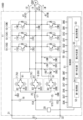
- FIG. 1 is a circuit diagram of a system including a power conversion device according to a first embodiment.
- Fig. 2A is a waveform diagram for explaining the relationship between the load current and the voltage across the regenerative capacitor when the power conversion device is operating normally.
- Fig. 2B is a waveform diagram for explaining the relationship between the load current and the voltage across the regenerative capacitor when the power conversion device is operating abnormally.
- Fig. 3A is a waveform diagram for explaining the relationship between the load current and the voltage across the regenerative capacitor when the U-phase switch in the power conversion device of the above-mentioned embodiment fails.
- Fig. 2A is a waveform diagram for explaining the relationship between the load current and the voltage across the regenerative capacitor when the power conversion device is operating normally.
- Fig. 3A is a waveform diagram for explaining the relationship between the load current and the voltage across the regenerative capacitor when the U-phase switch in the power conversion device of the above-mentioned embodiment fails.
- Fig. 1 is
- FIG. 3B is a waveform diagram for explaining the relationship between the load current and the voltage across the regenerative capacitor when the V-phase switch in the power conversion device of the above-mentioned embodiment fails.
- Fig. 3C is a waveform diagram for explaining the relationship between the load current and the voltage across the regenerative capacitor when the V-phase switch in the power conversion device of the above-mentioned embodiment fails.
- FIG. 4 is a diagram illustrating the operation of the power conversion device when hard switching occurs in the U-phase switching circuit.
- FIG. 5 is a waveform diagram for explaining the relationship between the load current and the voltage across the regenerative capacitor when the V-phase switch and the W-phase switch fail in the power conversion device.
- FIG. 6A is a waveform diagram for explaining the relationship between the load current and the voltage across the regenerative capacitor when the power conversion device is operating normally
- Fig. 6B is a waveform diagram for explaining the relationship between the load current and the voltage across the regenerative capacitor when the switches of the U-phase, V-phase, and W-phase in the power conversion device are faulty.
- FIG. 7 is an explanatory diagram of an operation when the control device in the power conversion device performs a basic operation when the load current is greater than 0 and the resonance capacitor is being charged.
- FIG. 8 is another operation explanatory diagram when the control device in the power conversion device performs a basic operation in the case where the load current is greater than 0 and the resonance capacitor is being charged.
- FIG. 7 is an explanatory diagram of an operation when the control device in the power conversion device performs a basic operation when the load current is greater than 0 and the resonance capacitor is being charged.
- FIG. 8 is another operation explanatory diagram when the control device in the power conversion device performs
- FIG. 9 is a diagram showing a time change in duty and a time change in load current corresponding to voltage commands for each of three phases in an AC load connected to a plurality of AC terminals of the power conversion device according to the above embodiment.
- FIG. 10 is an explanatory diagram of a first current threshold value and a second current threshold value used by a control device in the power conversion device according to the above embodiment.
- FIG. 11 is an explanatory diagram of an operation when the control device in the power conversion device performs a basic operation when the load current is greater than 0 and the resonant capacitor is discharging.
- FIG. 12 is an explanatory diagram of an operation when the control device in the power conversion device performs a basic operation when the load current is less than 0 and the resonant capacitor is discharging.
- FIG. 13 is an explanatory diagram of an operation when the control device in the power conversion device performs a basic operation when the load current is less than 0 and the resonance capacitor is being charged.
- FIG. 14 is a circuit diagram of a system including a power conversion device according to the second embodiment.
- FIG. 15 is a diagram illustrating the operation of the power conversion device.
- FIG. 16 is a diagram illustrating the operation of the power conversion device.
- FIG. 17 is a circuit diagram of a system including a power conversion device according to the third embodiment.
- FIG. 18 is a circuit diagram of a system including a power conversion device according to the fourth embodiment.
- FIG. 19 is a circuit diagram of a system including a power conversion device according to a first modification of the fourth embodiment.
- FIG. 20 is a circuit diagram of a system including a power conversion device according to a second modification of the fourth embodiment.
- FIG. 21 is a circuit diagram of a system including a power conversion device according to a third modification of the fourth embodiment.
- FIG. 22 is a circuit diagram of a system including a power conversion device according to a fourth modification of the fourth embodiment.
- FIG. 23 is a circuit diagram of a system including a power conversion device according to the fifth embodiment.
- the power conversion device 100 includes a first DC terminal 31, a second DC terminal 32, and a plurality of (e.g., three) AC terminals 41.
- a DC power source E1 is connected between the first DC terminal 31 and the second DC terminal 32, and an AC load RA1 is connected to the plurality of AC terminals 41.
- the AC load RA1 is, for example, a three-phase motor.
- the power conversion device 100 converts the DC output from the DC power source E1 into AC power and outputs it to the AC load RA1.
- the DC power source E1 includes, for example, a solar cell or a fuel cell.
- the DC power source E1 may include a DC-DC converter.
- the AC power is, for example, three-phase AC power having a U phase, a V phase, and a W phase.
- the power conversion device 100 includes a power conversion circuit 11, a plurality of (e.g., three) switches 8, a plurality of (e.g., three) resonant capacitors 9, a regenerative capacitor 15, a plurality of (e.g., three) resonant inductors L1, and a control device 50.
- the power conversion device 100 further includes a plurality of (e.g., three) protection circuits 17.
- Each of the plurality of switches 8 is, for example, a bidirectional switch.
- the power conversion circuit 11 has a plurality (e.g., three) of first switching elements 1 and a plurality (e.g., three) of second switching elements 2.
- a plurality (e.g., three) of switching circuits 10 in which a plurality of first switching elements 1 and a plurality of second switching elements 2 are connected in series in a one-to-one relationship, are connected in parallel with each other.
- a plurality of first switching elements 1 are connected to a first DC terminal 31, and a plurality of second switching elements 2 are connected to a second DC terminal 32.
- a plurality of AC terminals 41 correspond one-to-one to the plurality of switching circuits 10.
- Each of the plurality of AC terminals 41 is connected to a connection point 3 of the first switching element 1 and the second switching element 2 in a corresponding one of the plurality of switching circuits 10.
- a plurality of switches 8 correspond one-to-one to the plurality of switching circuits 10.
- Each of the plurality of switches 8 has a first end 81 and a second end 82.
- Each of the multiple switches 8 has a first end 81 connected to a connection point 3 between the first switching element 1 and the second switching element 2 in a corresponding switching circuit 10 among the multiple switching circuits 10.
- the multiple resonance capacitors 9 correspond one-to-one to the multiple switches 8.
- Each of the multiple resonance capacitors 9 is connected between the first end 81 and the second DC terminal 32 of the corresponding switch 8 among the multiple switches 8.
- Each of the multiple resonance inductors L1 has a third end and a fourth end.
- the fourth end is connected to the regenerative capacitor 15.
- the third end is connected to the second end 82 of the corresponding switch 8 among the multiple switches 8.
- the regenerative capacitor 15 has a fifth end 153 and a sixth end 154.
- the fifth end 153 is connected to the second DC terminal 32, and the sixth end 154 is connected to the fourth end of the regenerative inductor L1.
- the control device 50 controls a plurality of first switching elements 1, a plurality of second switching elements 2, and a plurality of switches 8.
- the switching circuits 10 corresponding to the U-phase, V-phase, and W-phase of the multiple switching circuits 10 may be referred to as a switching circuit 10U, a switching circuit 10V, and a switching circuit 10W, respectively.
- the first switching element 1 and the second switching element 2 of the switching circuit 10U may be referred to as a first switching element 1U and a second switching element 2U.
- the first switching element 1 and the second switching element 2 of the switching circuit 10V may be referred to as a first switching element 1V and a second switching element 2V.
- the first switching element 1 and the second switching element 2 of the switching circuit 10W may be referred to as a first switching element 1W and a second switching element 2W.
- the connection point 3 between the first switching element 1U and the second switching element 2U may be referred to as the connection point 3U
- the connection point 3 between the first switching element 1V and the second switching element 2V may be referred to as the connection point 3V
- the connection point 3 between the first switching element 1W and the second switching element 2W may be referred to as the connection point 3W.
- the AC terminal 41 connected to the connection point 3U may be referred to as the AC terminal 41U
- the AC terminal 41 connected to the connection point 3V may be referred to as the AC terminal 41V
- the AC terminal 41 connected to the connection point 3W may be referred to as the AC terminal 41W.
- the resonant capacitor 9 connected in parallel to the second switching element 2U may be referred to as the resonant capacitor 9U
- the resonant capacitor 9 connected in parallel to the second switching element 2V may be referred to as the resonant capacitor 9V
- the resonant capacitor 9 connected in parallel to the second switching element 2W may be referred to as the resonant capacitor 9W.
- switch 8U the switch 8 connected to connection point 3U
- switch 8V the switch 8 connected to connection point 3V
- switch 8W the switch 8 connected to connection point 3W
- the high-potential output terminal (positive electrode) of the DC power supply E1 is connected to the first DC terminal 31, and the low-potential output terminal (negative electrode) of the DC power supply E1 is connected to the second DC terminal 32.
- the U-phase terminal, V-phase terminal, and W-phase terminal of the AC load RA1 are connected to the three AC terminals 41U, 41V, and 41W, respectively.
- each of the multiple (e.g., three) first switching elements 1 and the multiple (e.g., three) second switching elements 2 has a control terminal, a first main terminal, and a second main terminal.
- the control terminals of the multiple first switching elements 1 and the multiple second switching elements 2 are connected to the control device 50.
- the first main terminal of the first switching element 1 is connected to the first DC terminal 31
- the second main terminal of the first switching element 1 is connected to the first main terminal of the second switching element 2
- the second main terminal of the second switching element 2 is connected to the second DC terminal 32.
- the first switching element 1 is a high-side switching element (P-side switching element), and the second switching element 2 is a low-side switching element (N-side switching element).
- Each of the multiple first switching elements 1 and the multiple second switching elements 2 is, for example, an IGBT (Insulated Gate Bipolar Transistor). Therefore, the control terminal, the first main terminal, and the second main terminal of each of the multiple first switching elements 1 and the multiple second switching elements 2 are the gate terminal, the collector terminal, and the emitter terminal, respectively.
- the power conversion circuit 11 further includes a plurality (three) of first diodes 4 connected in anti-parallel to a plurality (three) of first switching elements 1 in a one-to-one relationship, and a plurality (three) of second diodes 5 connected in anti-parallel to a plurality (three) of second switching elements 2 in a one-to-one relationship.
- the anode of the first diode 4 is connected to the second main terminal (emitter terminal) of the first switching element 1 corresponding to the first diode 4
- the cathode of the first diode 4 is connected to the first main terminal (collector terminal) of the first switching element 1 corresponding to the first diode 4.
- the anode of the second diode 5 is connected to the second main terminal (emitter terminal) of the second switching element 2 corresponding to the second diode 5, and the cathode of the second diode 5 is connected to the first main terminal (collector terminal) of the second switching element 2 corresponding to the second diode 5.
- connection point 3U between the first switching element 1U and the second switching element 2U is connected to, for example, the U-phase terminal of the AC load RA1 via the AC terminal 41U.
- connection point 3V between the first switching element 1V and the second switching element 2V is connected to, for example, the V-phase terminal of the AC load RA1 via the AC terminal 41V.
- connection point 3W between the first switching element 1W and the second switching element 2W is connected to, for example, the W-phase terminal of the AC load RA1 via the AC terminal 41W.
- the multiple resonant capacitors 9 correspond one-to-one to the multiple switches 8. Each of the multiple resonant capacitors 9 is connected between the first end 81 and the second DC terminal 32 of a corresponding switch 8 among the multiple switches 8.
- the power conversion device 100 has multiple resonant circuits. Each of the multiple resonant circuits includes a resonant capacitor 9 and a resonant inductor L1.
- Each of the multiple switches 8 has, for example, two first IGBTs 6 and second IGBTs 7 connected in inverse parallel.
- the collector terminal of the first IGBT 6 is connected to the emitter terminal of the second IGBT 7, and the emitter terminal of the first IGBT 6 is connected to the collector terminal of the second IGBT 7.
- the emitter terminal of the first IGBT 6 is connected to the connection point 3 of the switching circuit 10 corresponding to the switch 8 having the first IGBT 6.
- the collector terminal of the second IGBT 7 is connected to the connection point 3 of the switching circuit 10 corresponding to the switch 8 having the second IGBT 7.
- the switch 8U is connected to the connection point 3U of the first switching element 1U and the second switching element 2U.
- the switch 8V is connected to the connection point 3V of the first switching element 1V and the second switching element 2V.
- the switch 8W is connected to a connection point 3W between the first switching element 1W and the second switching element 2W.
- the first IGBT 6 and the second IGBT 7 of the switch 8U are referred to as the first IGBT 6U and the second IGBT 7U, respectively
- the first IGBT 6 and the second IGBT 7 of the switch 8V are referred to as the first IGBT 6V and the second IGBT 7V, respectively
- the first IGBT 6 and the second IGBT 7 of the switch 8W are referred to as the first IGBT 6W and the second IGBT 7W, respectively.
- the multiple switches 8 are controlled by the control device 50.
- the first IGBT 6U, the second IGBT 7U, the first IGBT 6V, the second IGBT 7V, the first IGBT 6W, and the second IGBT 7W are controlled by the control device 50.
- Each of the multiple resonant inductors L1 has a third end and a fourth end.
- the third end of each of the multiple resonant inductors L1 is connected to the second end 82 of a corresponding one of the multiple switches 8.
- the fourth end of each of the multiple resonant inductors L1 is connected to the sixth end 154 of the regenerative capacitor 15.
- the inductances of the multiple resonant inductors L1 are the same as each other. That is, the inductances of the three resonant inductors L1 are the same as each other.
- the regenerative capacitor 15 is connected between the fourth ends of the multiple resonant inductors L1 and the second DC terminal 32.
- the regenerative capacitor 15 is, for example, a film capacitor.
- Each of the multiple protection circuits 17 has a third diode 13 and a fourth diode 14.
- the third diode 13 is connected between the connection point between the resonance inductor L1 and the switch 8 and the first DC terminal 31.
- the anode of the third diode 13 is connected to the connection point between the resonance inductor L1 and the switch 8.
- the cathode of the third diode 13 is connected to the first DC terminal 31.
- the fourth diode 14 is connected between the connection point between the resonance inductor L1 and the switch 8 and the second DC terminal 32.
- the anode of the fourth diode 14 is connected to the second DC terminal 32.
- the cathode of the fourth diode 14 is connected to the connection point between the resonance inductor L1 and the switch 8. Therefore, in each of the multiple protection circuits 17, the fourth diode 14 is connected in series to the third diode 13.
- the control device 50 controls the multiple first switching elements 1, the multiple second switching elements 2, and the multiple switches 8.
- the control device 50 outputs control signals SU1, SV1, SW1 that control the on/off of each of the multiple first switching elements 1U, 1V, 1W.
- Each of the control signals SU1, SV1, SW1 is, for example, a PWM (Pulse Width Modulation) signal whose potential level changes between a first potential level (hereinafter also referred to as a low level) and a second potential level (hereinafter also referred to as a high level) that is higher than the first potential level.
- the first switching elements 1U, 1V, 1W are in an on state when the control signals SU1, SV1, SW1 are at a high level, and in an off state when the control signals are at a low level.
- the control device 50 also outputs control signals SU2, SV2, SW2 that control the on/off of each of the multiple second switching elements 2U, 2V, 2W.
- Each of the control signals SU2, SV2, and SW2 is, for example, a PWM signal whose potential level changes between a first potential level (hereinafter also referred to as a low level) and a second potential level (hereinafter also referred to as a high level) that is higher than the first potential level.
- the second switching elements 2U, 2V, and 2W are turned on when the control signals SU2, SV2, and SW2 are at a high level, and turned off when they are at a low level.
- the control device 50 uses a sawtooth carrier signal (see FIG. 7) to generate control signals SU1, SV1, SW1 corresponding to each of the first switching elements 1U, 1V, 1W, and control signals SU2, SV2, SW2 corresponding to each of the second switching elements 2U, 2V, 2W. More specifically, the control device 50 generates control signals SU1, SU2 to be provided to the first switching element 1U and the second switching element 2U, respectively, based on at least the carrier signal and a voltage command for the U phase. The control device 50 also generates control signals SV1, SV2 to be provided to the first switching element 1V and the second switching element 2V, respectively, based on at least the carrier signal and a voltage command for the V phase.
- a sawtooth carrier signal see FIG. 7
- the control device 50 also generates control signals SW1, SW2 to be provided to the first switching element 1W and the second switching element 2W, respectively, based on at least the carrier signal and a voltage command for the W phase.
- the U-phase voltage command, V-phase voltage command, and W-phase voltage command are, for example, sinusoidal signals with a phase difference of 120°, and the values (voltage command values) change over time.
- the waveform of the carrier signal is not limited to a sawtooth waveform, and may be, for example, a triangular wave or a sawtooth wave obtained by inverting the sawtooth wave shown in FIG. 7.
- the length of one cycle of the U-phase voltage command, V-phase voltage command, and W-phase voltage command is the same.
- the length of one cycle of the U-phase voltage command, V-phase voltage command, and W-phase voltage command is longer than the length of one cycle of the carrier signal.
- the duty of the control signal SU1 is shown as the U-phase duty.
- the control device 50 compares the U-phase voltage command with the carrier signal to generate the control signal SU1 to be provided to the first switching element 1U.
- the control device 50 also inverts the control signal SU1 to be provided to the first switching element 1U to generate the control signal SU2 to be provided to the second switching element 2U.
- the control device 50 also sets a dead time period Td (see FIG. 7) between the high-level period of the control signal SU1 and the high-level period of the control signal SU2 so that the on periods of the first switching element 1U and the second switching element 2U do not overlap.
- the duty of the control signal SV1 is shown as the V-phase duty.
- the control device 50 compares the V-phase voltage command with the carrier signal to generate the control signal SV1 to be provided to the first switching element 1V.
- the control device 50 also inverts the control signal SV1 to be provided to the first switching element 1V to generate the control signal SV2 to be provided to the second switching element 2V.
- the control device 50 also sets a dead time period Td (see FIG. 7) between the high-level period of the control signal SV1 and the high-level period of the control signal SV2 so that the on periods of the first switching element 1V and the second switching element 2V do not overlap.
- the duty of the control signal SW1 is shown as the W phase duty.
- the control device 50 compares the voltage command of the W phase with the carrier signal to generate the control signal SW1 to be provided to the first switching element 1W.
- the control device 50 also inverts the control signal SW1 to be provided to the first switching element 1W to generate the control signal SW2 to be provided to the second switching element 2W.
- the control device 50 also sets a dead time period Td (see FIG. 8) between the high level period of the control signal SW1 and the high level period of the control signal SW2 so that the on periods of the first switching element 1W and the second switching element 2W do not overlap.
- the U-phase voltage command, V-phase voltage command, and W-phase voltage command are, for example, sinusoidal signals whose phases differ by 120°, and whose values change over time. Therefore, the duty of the control signal SU1 (U-phase duty), the duty of the control signal SV1 (V-phase duty), and the duty of the control signal SW1 (W-phase duty) change in sinusoidal forms whose phases differ by 120°, for example, as shown in FIG. 9. Similarly, the duty of the control signal SU2, the duty of the control signal SV2, and the duty of the control signal SW2 change in sinusoidal forms whose phases differ by 120°.
- the control device 50 generates the control signals SU1, SU2, SV1, SV2, SW1, and SW2 based on the carrier signal, the voltage commands, and information about the state of the AC load RA1.
- the information about the state of the AC load RA1 includes, for example, detection values from a plurality of current sensors that detect output currents (hereinafter also referred to as load currents) iU, iV, and iW that flow through the U-phase, V-phase, and W-phase of the AC load RA1, respectively.
- the multiple switches 8, multiple resonant inductors L1, multiple resonant capacitors 9, and regenerative capacitor 15 are provided to perform zero-voltage soft switching of the multiple first switching elements 1 and the multiple second switching elements 2.
- control device 50 controls a plurality of switches 8 in addition to a plurality of first switching elements 1 and second switching elements 2 of the power conversion circuit 11.
- the control device 50 generates control signals SU6, SU7, SV6, SV7, SW6, SW7 that control the on/off of the first IGBT6U, the second IGBT7U, the first IGBT6V, the second IGBT7V, the first IGBT6W, and the second IGBT7W, and outputs them to the gate terminals of the first IGBT6U, the second IGBT7U, the first IGBT6V, the second IGBT7V, the first IGBT6W, and the second IGBT7W.
- the switch 8U can pass a charging current that flows through the path of the regenerative capacitor 15 - resonant inductor L1 - switch 8U - resonant capacitor 9U.
- the charging current is a current that charges the resonant capacitor 9U.
- the switch 8U can pass a discharging current that flows through the path of the resonant capacitor 9U - switch 8U - resonant inductor L1 - regenerative capacitor 15.
- the discharging current is a current that discharges the charge in the resonant capacitor 9U.
- the switch 8V can pass a charging current that flows through the path of the regenerative capacitor 15 - resonant inductor L1 - switch 8V - resonant capacitor 9V.
- the charging current is a current that charges the resonant capacitor 9V.
- the switch 8V can pass a discharging current that flows through the path of the resonant capacitor 9V - switch 8V - resonant inductor L1 - regenerative capacitor 15.
- the discharging current is a current that discharges the charge of the resonant capacitor 9V.
- the switch 8W can pass a charging current that flows through the path of the regenerative capacitor 15 - resonant inductor L1 - switch 8W - resonant capacitor 9W.
- the charging current is a current that charges the resonant capacitor 9W.
- the switch 8W can pass a discharging current that flows through the path of the resonant capacitor 9W - switch 8W - resonant inductor L1 - regenerative capacitor 15.
- the discharging current is a current that discharges the charge of the resonant capacitor 9W.
- the control device 50 has a control unit 51, a first acquisition unit 52, a second acquisition unit 53, a first judgment unit 54, and a second judgment unit 55.
- the control unit 51 has a function of controlling the on/off of each of the multiple first switching elements 1, the multiple second switching elements 2, and the multiple switches 8.
- the control unit 51 has a function of generating each control signal SU1, SU2, SV1, SV2, SW1, SW2 based on the above-mentioned carrier signal, each voltage command, and information regarding the state of the AC load RA1.
- the information regarding the state of the AC load RA1 includes detection values from multiple current sensors that detect load currents iU, iV, iW.
- the first acquisition unit 52 has the function of acquiring the detection value of the voltage sensor 20 that detects the voltage V15 across the regenerative capacitor 15.
- the second acquisition unit 53 has a function of acquiring detection values from the multiple current sensors described above. In other words, the second acquisition unit 53 has a function of acquiring detection values of multiple load currents iU, iV, iW output from the multiple AC terminals 41.
- Each of the multiple load currents iU, iV, iW is, for example, a sinusoidal AC current.
- the multiple load currents iU, iV, iW are, for example, out of phase with each other by 120°.
- the first determination unit 54 determines the switching state in the power conversion circuit 11 based on the ripple voltage included in the voltage V15 across the regenerative capacitor 15 and the multiple load currents iU, iV, iW output from the multiple AC terminals 41.
- the switching state in the power conversion circuit 11 includes at least one of the switching states of the multiple first switching elements 1 and the multiple second switching elements 2.
- "determining the switching state in the power conversion circuit 11” means determining whether or not hard switching occurs in the power conversion circuit 11.
- Hard switching has occurred in the power conversion circuit 11 means that hard switching has occurred in at least one of the multiple first switching elements 1 and the multiple second switching elements 2.
- the second judgment unit 55 judges which of the multiple switching circuits 10 is experiencing hard switching.
- the second judgment unit 55 judges which of the multiple switching circuits 10 is experiencing hard switching based on the polarities of the multiple load currents iU, iV, iW at a specific phase of the ripple voltage contained in the voltage V15 across the regenerative capacitor 15.
- the operation of the second judgment unit 55 will be described in more detail in the section "(3.2) Operation of the first judgment unit and the second judgment unit".
- the executing entity of the control device 50 includes a computer system.
- the computer system has one or more computers.
- the computer system is mainly composed of a processor and a memory as hardware.
- the processor executes a program recorded in the memory of the computer system, thereby realizing the function of the executing entity of the control device 50 in this disclosure.
- the program may be pre-recorded in the memory of the computer system, or may be provided through an electric communication line, or may be recorded and provided on a non-transitory recording medium such as a memory card, an optical disk, or a hard disk drive (magnetic disk) that can be read by the computer system.
- the processor of the computer system is composed of one or more electronic circuits including a semiconductor integrated circuit (IC) or a large-scale integrated circuit (LSI).
- the multiple electronic circuits may be integrated in one chip or distributed across multiple chips.
- the multiple chips may be integrated in one device or distributed across multiple devices.
- the polarity of the current iL1 flowing through the resonant inductor L1 is defined as positive when it flows in the direction of the arrow in Fig. 1, and the polarity of the current flowing in the opposite direction to the direction of the arrow in Fig. 1 is defined as negative.
- the polarity of the load currents iU, iV, and iW flowing through the U-phase, V-phase, and W-phase of the AC load RA1 is defined as positive when it flows in the direction of the arrow in Fig.
- the control device 50 sets a dead time period Td between the high level period of the control signals SU1, SV1, SW1 to the first switching elements 1U, 1V, 1W and the high level period of the control signals SU2, SV2, SW2 to the second switching elements 2U, 2V, 2W for each of the multiple switching circuits 10.
- control device 50 for realizing zero voltage soft switching of each of the multiple first switching elements 1 and the multiple second switching elements 2 will be explained with reference to Figures 1 and 7 to 13, and then the operation of the first determination unit 54 and the second determination unit 55 will be explained with reference to Figures 2A, 2B, 3A, 3B, 3C, 4, 5, 6A, and 6B.
- the basic operation of the control device 50 differs depending on the polarity (positive/negative) of the load current flowing through the AC terminal 41 connected to the target switching element and the operation (charging operation/discharging operation) of the resonant capacitor 9 connected in series or parallel to the target switching element.
- the load currents iU, iV, and iW are positive when they flow from the AC terminal 41 to the AC load RA1, and negative when they flow from the AC load RA1 to the AC terminal 41.
- the resonant capacitor 9 is charging, the voltage across the resonant capacitor 9 increases.
- the resonant capacitor 9 is discharging, the voltage across the resonant capacitor 9 decreases.
- the voltage across each of the multiple second switching elements 2 is the same as the voltage across the resonant capacitor 9 connected in parallel to the second switching element 2.
- the basic operation of the control device 50 is executed by the control unit 51.
- the control device 50 turns on the first IGBT 6 corresponding to the target first switching element 1.
- the control device 50 causes the resonant inductor L1 and the resonant capacitor 9 connected to the target first switching element 1 to resonate, charging the resonant capacitor 9 from the regenerative capacitor 15, and setting the voltage across the target first switching element 1 to zero.
- the power conversion device 100 can realize zero-voltage soft switching of the target first switching element 1.
- FIG. 7 shows the control signals SU1 and SU2 given from the control device 50 to the first switching element 1U and the second switching element 2U of the switching circuit 10U when the target first switching element is the first switching element 1U of the switching circuit 10U. Also shown in Fig. 7 are the control signal SU6 given from the control device 50 to the first IGBT 6U of the switch 8U, the load current iU flowing in the U-phase of the AC load RA1, the current iL1 flowing in the resonant inductor L1, the voltage V1u across the first switching element 1U, and the voltage V2u across the second switching element 2U. Also shown in Fig.
- FIG. 7 are the control signals SV1 and SV2 given from the control device 50 to the first switching element 1V and the second switching element 2V of the switching circuit 10V when the target first switching element is the first switching element 1V of the switching circuit 10V.
- FIG. 7 also illustrates the control signal SV6 provided from the control device 50 to the first IGBT 6V of the switch 8V, the load current iV flowing through the V phase of the AC load RA1, the current iL1 flowing through the resonant inductor L1, the voltage V1v across the first switching element 1V, and the voltage V2v across the second switching element 2V.
- FIG. 7 also illustrates the dead time period Td that is set in the control device 50 to prevent the first switching element 1 and the second switching element 2, which are in phase, from being turned on at the same time.
- FIG. 7 also illustrates the additional time Tau that is set in the control device 50 for the control signal SU6 of the first IGBT 6U of the switch 8U, and the additional time Tav that is set for the control signal SV6 of the first IGBT 6V of the switch 8V.
- the additional time Tau and the additional time Tav will be described later.
- FIG. 8 illustrates control signals SW1 and SW2 provided from the control device 50 to the first switching element 1W and the second switching element 2W of the switching circuit 10W, respectively, when the target first switching element is the first switching element 1W of the switching circuit 10W.
- FIG. 8 illustrates the control signal SW6 provided from the control device 50 to the first IGBT 6W of the switch 8W, and the load current iW flowing through the W phase of the AC load RA1.
- FIG. 8 also illustrates the current iL1 flowing through the resonant inductor L1.
- FIG. 8 also illustrates the voltage V1w across the first switching element 1W and the voltage V2w across the second switching element 2W.
- the voltage value of the DC power source E1 is illustrated as Vd.
- FIG. 8 also illustrates the dead time period Td that is set in the control device 50 to prevent the first switching element 1W and the second switching element 2W from being turned on at the same time.
- FIG. 8 also illustrates the additional time Taw that is set in the control device 50 for the control signal SW6 of the first IGBT 6W of the switch 8W. The additional time Taw will be described later.
- the above-mentioned additional time Tau is a time set to make the high level period of the control signal SU6 longer than the dead time period Td by bringing the time t1 at which the high level period of the control signal SU6 starts earlier than the time t2 at which the dead time period Td starts, as shown in FIG. 7.
- the length of the additional time Tau is set based on the value of the load current iU. In order to start LC resonance from the time t2 at which the dead time period Td starts, it is desirable that the value of the current iL1 matches the value of the load current iU at the time t2 at which the dead time period Td starts.
- the time at which the high level period of the control signal SU6 ends may be the same as the time t3 at which the dead time period Td ends or later.
- FIG. 7 shows an example in which the time at which the high level period of the control signal SU6 ends is set to the same as the time t3 at which the dead time period Td ends.
- the control device 50 sets the length of the high-level period of the control signal SU6 to Tau+Td.
- the voltage V2u across the second switching element 2U becomes Vd at time t3 when the dead-time period Td ends, and the voltage V1u across the first switching element 1U becomes zero at time t3 when the dead-time period Td ends.
- the current iL1 flowing through the resonance inductor L1 starts to flow at time t1 when the high-level period of the control signal SU6 starts, and becomes zero at time t4 when the additional time Tau has elapsed from time t3 when the dead-time period Td ends.
- the current iL1 since iL1 ⁇ iU from time t2 when the dead-time period Td starts, the current iL1 in the shaded area of the current waveform in the fifth row from the top in FIG. 7 flows into the resonance capacitor 9U, and LC resonance occurs. After time t3 when the dead time period Td ends, the current iL1 is regenerated in the power conversion circuit 11 via the third diode 13 that is directly connected to the resonant inductor L1.
- the detection value at the carrier period to which the additional time Tau is added, or at the timing closest to that carrier period is used.
- the estimated value of the load current iU at this time the value estimated from the load current iU at the carrier period to which the additional time Tau is added, is used.
- the resonant half cycle is half the resonant cycle, which is the reciprocal of the resonant frequency of a resonant circuit including one resonant inductor L1 and one resonant capacitor 9.
- the resonant half cycle is set to be equal to or shorter than the length of the dead time period Td, and as an example, is set to be equal to the length of the dead time period Td.
- the above-mentioned additional time Tav is a time set to make the high level period of the control signal SV6 longer than the dead time period Td by bringing the start time t5 of the high level period of the control signal SV6 earlier than the start time t6 of the dead time period Td, as shown in FIG. 7.
- the length of the additional time Tav is set based on the value of the load current iV. In order to start LC resonance from the start time t6 of the dead time period Td, it is desirable that the value of the current iL1 matches the value of the load current iV at the start time t6 of the dead time period Td.
- the time at which the high level period of the control signal SV6 ends may be the same as or later than the time t7 at which the dead time period Td ends.
- FIG. 7 shows an example in which the time at which the high level period of the control signal SV6 ends is set to the same as the time t7 at which the dead time period Td ends.
- the control device 50 sets the length of the high-level period of the control signal SV6 to Tav+Td.
- the voltage V1v across the first switching element 1V becomes zero at time t7 when the dead-time period Td ends.
- the current iL1 flowing through the resonant inductor L1 starts flowing at time t5 when the high-level period of the control signal SV6 starts, and becomes zero at time t8 when the additional time Tav has elapsed from time t7 when the dead-time period Td ends.
- the current iL1 in the shaded area of the current waveform in the 10th row from the top in FIG. 7 flows into the resonant capacitor 9V, and LC resonance occurs.
- the current iL1 is regenerated to the power conversion circuit 11 via the third diode 13 directly connected to the resonant inductor L1.
- the detection value at the carrier period to which the additional time Tav is added, or at the timing closest to that carrier period is used.
- the estimated value of the load current iV at this time the value estimated from the load current iV at the carrier period to which the additional time Tav is added, is used.
- the above-mentioned additional time Taw is a time set to make the high level period of the control signal SW6 longer than the dead time period Td by bringing the start time t9 of the high level period of the control signal SW6 earlier than the start time t10 of the dead time period Td, as shown in FIG. 8.
- the length of the additional time Taw is set based on the value of the load current iW. In order to start LC resonance from the start time t10 of the dead time period Td, it is desirable that the value of the current iL1 matches the value of the load current iW at the start time t10 of the dead time period Td.
- the end time of the high level period of the control signal SW6 may be the same as or later than the end time t11 of the dead time period Td.
- FIG. 8 shows an example in which the end time of the high level period of the control signal SW6 is set to the same as the end time t11 of the dead time period Td.
- the control device 50 sets the length of the high-level period of the control signal SW6 to Taw+Td. The voltage V1w across the first switching element 1W becomes zero at time t11 when the dead-time period Td ends.
- FIG. 8 shows an example in which the end time of the high level period of the control signal SW6 is set to the same as the end time t11 of the dead time period Td.
- the current iL1 flowing through the resonant inductor L1 starts to flow at time t9 when the high-level period of the control signal SW6 starts, and becomes zero at time t12 when the additional time Taw has elapsed from time t11 when the dead-time period Td ends.
- the current iL1 in the shaded area of the current waveform in the fourth row from the top in FIG. 8 flows into the resonant capacitor 9W, and LC resonance occurs.
- the current iL1 is regenerated to the power conversion circuit 11 via the third diode 13 directly connected to the resonant inductor L1.
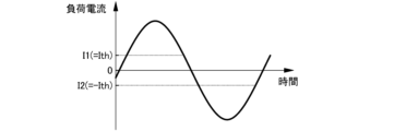
- the control device 50 when the current value of the load current is greater than the first current threshold I1, the control device 50 can discharge the resonance capacitor 9 connected in parallel to the target second switching element 2 by the load current without turning on the switch 8 corresponding to the target second switching element 2. This enables the power conversion device 100 to realize zero voltage soft switching of the target second switching element 2 .
- Figure 11 shows the control signals SU1, SU2, and SU7, the load current iU, the current i9U flowing from the resonant capacitor 9U, and the voltage V2u across the second switching element 2U when the target second switching element 2 is the second switching element 2U of the switching circuit 10U and the current value of the load current iU is greater than the first current threshold I1.
- Figure 11 also shows the dead time period Td and the additional time Tau set in the control device 50 for the control signal SU7 to the second IGBT 7U of the switch 8U.
- the control device 50 When the current value of the load current iU is greater than the first current threshold I1, the control device 50 does not set a high level period for the control signal SU7.
- the current i9U starts to flow from the resonant capacitor 9U at time t22 when the dead time period Td starts, and the current i9U drops to zero before time t23 when the dead time period Td ends, and the voltage V2u across the second switching element 2U becomes zero before time t23 when the dead time period Td ends.
- the control signal SU2 changes from low level to high level at time t23 when the dead time period Td ends, the second switching element 2U is soft-switched to zero voltage.
- the control device 50 When the current value of the load current iU is smaller than the first current threshold I1, the control device 50 provides a high-level period for the control signal SU7, for example, as shown by the two-dot chain line in FIG. 11.
- the start time of the high-level period of the control signal SU7 at this time is, for example, the same as the start time t22 of the dead time period Td.
- the end time of the high-level period of the control signal SU7 is the same as the end time t23 of the dead time period Td.
- the second switching element 2U when the control signal SU2 changes from a low level to a high level at the end time t23 of the dead time period Td, the second switching element 2U is zero-voltage soft-switched.
- the start time of the high-level period of the control signal SU7 may be time t21, which is earlier than the start time t22 of the dead time period Td by an additional time Tau.
- the end point of the high level period of the control signal SU7 may be time t24, which is later than time t23 at which the dead time period Td ends by the additional time Tau. Note that the time before and after the period in which the high level period of the control signal SU7 overlaps with the dead time period Td is not limited to the additional time Tau, and may be another set time.
- control signals SU1, SU2, and SU7 the load current iU, the current iL1 flowing through the resonant inductor L1, and the voltage V2u across the second switching element 2U are shown for the case where the target second switching element 2 is the second switching element 2U of the switching circuit 10U.
- FIG. 12 also illustrates the dead time period Td set in the control device 50 to prevent the first switching element 1 and the second switching element 2 of the same phase from being turned on at the same time.
- FIG. 12 also illustrates the additional time Tau set in the control device 50 for the control signal SU7 of the second IGBT 7U of the switch 8U.
- the end point of the high level period of the control signal SU7 may be the same as the end point t33 of the dead time period Td or later.
- FIG. 12 illustrates an example in which the end point of the high level period of the control signal SU7 is set to the same as the end point t33 of the dead time period Td.
- the control device 50 sets the length of the high level period of the control signal SU7 to Tau+Td.
- the voltage V2u across the second switching element 2U becomes zero at the end point t33 of the dead time period Td.
- the current iL1 flowing through the resonant inductor L1 starts at time t31 when the high-level period of the control signal SU7 starts, and becomes zero at time t34 when the additional time Tau has elapsed from time t33 when the dead-time period Td ends.
- the detection result of the load current iU or its signal processing value is the detection value at the carrier period to which the additional time Tau is added, or at the timing closest to that carrier period.
- the estimated value of the load current iU at this time is, for example, the estimated value of the load current iU in the carrier period to which the additional time Tau is added.
- the power conversion device 100 can charge the resonance capacitor 9 connected in series to the target first switching element 1 with the load current without the control device 50 turning on the switch 8 corresponding to the target first switching element 1. This allows the power conversion device 100 to realize zero-voltage soft switching of the target first switching element 1.
- the target first switching element 1 is the first switching element 1U of the switching circuit 10U, and the control signals SU1, SU2, and SU6, the load current iU, the current i9U flowing from the resonant capacitor 9U, the voltage V1u across the first switching element 1U, and the voltage V2u across the second switching element 2U are shown for the case where the target first switching element 1 is the first switching element 1U of the switching circuit 10U, and the current value of the load current iU is greater than the second current threshold I2 (in other words, the absolute value of the current value of the load current iU is less than the absolute value of the second current threshold I2).
- FIG. 13 also shows the carrier signal and the dead time period Td.
- the control device 50 does not provide a high-level period for the control signal SU6.
- the current i9U starts to flow through the resonant capacitor 9U at time t41 when the dead time period Td starts.
- the resonant capacitor 9U is charged and the voltage V2u across the second switching element 2U increases, the current i9U becomes zero before time t42 when the dead time period Td ends, and the voltage V1u across the first switching element 1U becomes zero before time t42 when the dead time period Td ends.
- the first switching element 1U is zero-voltage soft-switched.
- the control device 50 When the current value of the load current iU is greater than the second current threshold I2 (in other words, when the absolute value of the load current iU is less than the absolute value of the second current threshold I2), the control device 50 provides a high-level period for the control signal SU6, for example as shown by the two-dot chain line in FIG. 13.
- the point at which the high-level period of the control signal SU6 starts is the same as the point at which the dead-time period Td starts, t41.
- the point at which the high-level period of the control signal SU6 ends is the same as the point at which the dead-time period Td ends, t42.
- the voltage V1u across the first switching element 1U becomes zero before the point at which the dead-time period Td ends, t42. Therefore, in the power conversion device 100, when the control signal SU1 changes from low level to high level at the point at which the dead-time period Td ends, the first switching element 1U is zero-voltage soft-switched.
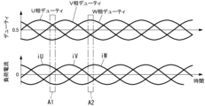
- the load current iU, the load current iV, the load current iW, and the voltage V15 across the regenerative capacitor 15 are shown to explain the operation when the switch 8U of the U phase fails.
- the vertical scale is shown to make it easier to see the maximum value Vmax and the minimum value Vmin of the ripple voltage contained in the voltage V15 across the regenerative capacitor 15.
- the ripple voltage of the voltage V15 across the regenerative capacitor 15 in FIG. 2A is the ripple voltage when all three switches 8U, 8V, and 8W are operating normally.
- the voltage V15 across the regenerative capacitor 15 is approximately Vd/2.
- 2B is the ripple voltage when the switch 8U of the three switches 8U, 8V, and 8W fails and is in an open state (off state).
- the switch 8U fails, the resonant capacitor 9U connected to the switch 8U is no longer charged or discharged, and the first switching element 1U and the second switching element 2U connected to the switch 8U are hard-switched.
- the resonant current of the U phase decreases, and one period of the ripple voltage included in the voltage V15 across the regenerative capacitor 15 becomes longer than one period of the ripple voltage included in the voltage V15 across the regenerative capacitor 15 when the switch 8U does not fail.
- the first determination unit 54 determines the switching state in the power conversion circuit 11 based on the ripple voltage contained in the voltage V15 across the regenerative capacitor 15 and the multiple load currents iU, iV, iW output from the multiple AC terminals 41.
- the switching state in the power conversion circuit 11 includes the switching states of the multiple first switching elements 1 and the multiple second switching elements 2.
- the first judgment unit 54 judges that hard switching is occurring in the power conversion circuit 11 when a predetermined condition (hereinafter also referred to as the first predetermined condition) is satisfied.
- “Hard switching is occurring in the power conversion circuit 11” means that hard switching is occurring in at least one of the multiple first switching elements 1 and the multiple second switching elements 2.
- the first predetermined condition is a condition in which the number of intersections B1 of any two load currents among the multiple load currents iU, iV, iW in a specified period Ts is greater than a specified value (e.g., 2).
- the specified period Ts is the period between the first occurrence timing tg1 of the first peak P1 of the ripple voltage and the second occurrence timing tg2 of the second peak P2 of the ripple voltage.
- the first peak P1 is one maximum peak at which the ripple voltage reaches the maximum value Vmax
- the second peak P2 is one maximum peak at which the ripple voltage reaches the maximum value Vmax after the first peak P1 (after the first peak P1 in the first embodiment).
- the first peak P1 is one of the multiple maximum peaks at which the ripple voltage reaches the maximum value Vmax
- the second peak P2 is the next maximum peak of the multiple maximum peaks after the one maximum peak.
- the length of the specified period Ts is the same as the length of one cycle of the ripple voltage.
- the two load currents have the same polarity and magnitude.
- the number of intersections B1 in the specified period Ts is two, whereas in FIG. 2B, the number of intersections B1 in the specified period Ts is seven, which is greater than two.
- the second peak P2 used in the first predetermined condition in the first judgment unit 54 may be one maximum value peak at which the ripple voltage reaches the maximum value Vmax after the first peak P1, for example, one maximum value peak at which the ripple voltage reaches the maximum value Vmax two times after the first peak P1.
- the length of the specified period Ts is twice the length of one cycle of the ripple voltage
- the specified value used in the first judgment unit 54 may be two times the value when the length of the specified period Ts is one cycle of the ripple voltage, that is, 4 times 2.
- the second peak P2 used in the first predetermined condition in the first judgment unit 54 may be one maximum value peak at which the ripple voltage reaches the maximum value Vmax three times after the first peak P1, for example.
- the length of the specified period Ts is three times the length of one cycle of the ripple voltage
- the specified value used in the first judgment unit 54 may be three times the value when the length of the specified period Ts is one cycle of the ripple voltage, that is, 6 times 2.
- the specified value used by the first judgment unit 54 may be appropriately determined according to the length of the specified period Ts. In other words, if the length of the specified period Ts is n cycles of the ripple voltage (n is a natural number), the specified value may be set to n x 2.
- the first judgment unit 54 uses a moving average as a signal processing value of the detection results of each of the load currents iU, iV, iW and the voltage V15 across the regenerative capacitor 15 in order to determine whether the first predetermined condition is satisfied.
- Each period for calculating the moving average can be set arbitrarily as long as it avoids exactly one cycle of the fluctuation cycle of each of the load currents iU, iV, iW and the voltage V15 across the regenerative capacitor 15. This makes it possible for the first judgment unit 54 to be less susceptible to the influence of noise contained in the detection values of each of the load currents iU, iV, iW and the voltage V15 across the regenerative capacitor 15, thereby improving the judgment accuracy.
- the first judgment unit 54 can improve the detection accuracy of each of the first peak P1, the second peak P2, and each intersection B1, and can improve the judgment accuracy of whether hard switching is occurring in the power conversion circuit 11.
- the first determination unit 54 may determine that each of the first switching elements 1 and the second switching elements 2 is soft-switched when a predetermined condition (hereinafter also referred to as a second predetermined condition) different from the first predetermined condition is satisfied. "Each of the first switching elements 1 and the second switching elements 2 is soft-switched" means, in other words, that "hard switching is not occurring in the power conversion circuit 11."
- the second predetermined condition is a condition that the number of intersections B1 of any two load currents among the multiple load currents iU, iV, and iW during the specified period Ts is equal to or less than a specified value.
- the specified period Ts is the period between the first occurrence timing tg1 of the first peak P1 of the ripple voltage and the second occurrence timing tg2 of the second peak P2 of the ripple voltage.
- the control device 50 stops the operation of the power conversion circuit 11, for example, after making a judgment using the second judgment unit 55.
- the control unit 51 sets each of the control signals SU1, SV1, SW1, SU2, SV2, and SW2 to a low level, or stops outputting the control signals SU1, SV1, SW1, SU2, SV2, and SW2.
- the second determination unit 55 determines which of the multiple switching circuits 10 is experiencing hard switching based on the polarities of the multiple load currents iU, iV, and iW at a specific phase of the ripple voltage.
- the load current iU flows so that the resonant capacitor 9U is discharged
- the load current iV flows so that the resonant capacitor 9V is discharged
- the load current iW flows so that the resonant capacitor 9W is charged.
- the polarity of the load current iU will be negative, the polarity of the load current iV will be positive, and the polarity of the load current iW will be positive, as shown in FIG. 3B.
- the switch 8V fails, the resonant capacitor 9V connected to the switch 8V will no longer be charged or discharged, and the switching of the first switching element 1V and second switching element 2V connected to the switch 8V will become hard switching.
- the specific phase is, for example, the first occurrence timing tg1 of the first peak P1 of the ripple voltage.
- the first peak P1 is a maximum value peak at which the ripple voltage reaches a maximum value Vmax.
- the specific phase is the phase of one of the multiple maximum value peaks of the ripple voltage of the voltage V15 across the regenerative capacitor 15.
- the second determination unit 55 determines that hard switching is occurring in the first switching element 1U and the second switching element 2U of the switching circuit 10U corresponding to the load current iU that is 120° out of phase with the load current iW.
- the second judgment unit 55 judges that hard switching is occurring in the first switching element 1V and the second switching element 2V of the switching circuit 10V corresponding to the load current iV, which is 120° out of phase with the load current iU.
- the second determination unit 55 determines that hard switching is occurring in the first switching element 1W and the second switching element 2W of the switching circuit 10W corresponding to the load current iW that is 120° out of phase with the load current iV.
- the second determination unit 55 can determine that the switching circuit 10V is experiencing hard switching.
- the second determination unit 55 determines that hard switching has occurred in the switching circuit 10 corresponding to the load current that is 120° out of the multiple switching circuits 10 and that is delayed in phase from the one load current, based on the load current that has the larger absolute value among the two load currents.
- the load current iU may not become zero at the first generation timing tg1 and the polarity of the load current iU may become negative.
- the second judgment unit 55 judges that hard switching has occurred in the first switching element 1W and the second switching element 2W of the switching circuit 10W corresponding to the load current iW that is 120° behind the load current iV among the multiple switching circuits 10, based on the load current iV that has the larger absolute value among the two load currents iU and iV.
- the first judgment unit 54 judges that hard switching is occurring in each of the multiple switching circuits 10 when the voltage V15 across the regenerative capacitor 15 is constant (see FIG. 6B).
- the voltage V15 across the regenerative capacitor 15 is constant means, for example, that the voltage V15 across the regenerative capacitor 15 in one cycle of the load current is within a range of 95% to 105% of the average value of the maximum value Vmax and minimum value Vmin of the ripple voltage when the three switches 8U, 8V, and 8W are not malfunctioning.
- the ripple voltage of the voltage V15 across the regenerative capacitor 15 in FIG. 6A is the ripple voltage when all three switches 8U, 8V, and 8W are operating normally.
- the control device 50 has a first determination unit 54 and a second determination unit 55.
- the first determination unit 54 determines the switching state in the power conversion circuit 11 based on the ripple voltage included in the voltage V15 across the regenerative capacitor 15 and the multiple load currents iU, iV, iW output from the multiple AC terminals 41.
- the second determination unit 55 determines which of the multiple switching circuits 10 is experiencing hard switching based on the polarities of the multiple load currents iU, iV, iW in a specific phase of the ripple voltage.
- the power conversion device 100 makes it possible to detect the switching circuit 10 in which hard switching occurs in the power conversion circuit 11.
- the power conversion device 100 can reduce costs by reducing the number of parts compared to a case where six voltage sensors are provided to detect the voltages across each of the three first switching elements 1 and the three second switching elements 2 of the power conversion circuit 11, and can also reduce the number of input ports required for the computer system (processor) that constitutes the control device 50.
- the first determination unit 54 determines that hard switching has occurred in the power conversion circuit 11 when a predetermined condition (first predetermined condition) is satisfied.
- the predetermined condition is that the number of intersections B1 of any two of the load currents iU, iV, and iW in the specified period Ts is greater than a specified value.
- the specified period Ts is the period between the first occurrence timing tg1 of the first peak P1 of the ripple voltage and the second occurrence timing tg2 of the second peak P2 of the ripple voltage. Therefore, the power conversion device 100 according to the first embodiment can detect that hard switching has occurred in the power conversion circuit 11 when hard switching has occurred in at least one of the first switching elements 1 and the second switching elements 2.
- the overall configuration of the power conversion device 100A according to the second embodiment is substantially the same as that of the power conversion device 100 according to the first embodiment (see Fig. 1), and differs from the power conversion device 100 according to the first embodiment in that a second determination unit 55A is provided instead of the second determination unit 55 of the control device 50 in the power conversion device 100.
- a second determination unit 55A is provided instead of the second determination unit 55 of the control device 50 in the power conversion device 100.
- components similar to those of the power conversion device 100 according to the first embodiment are denoted by the same reference numerals and description thereof is omitted.
- the second determination unit 55A determines which of the multiple switching circuits 10 is experiencing hard switching based on the control signals SU6, SU7, SV6, SV7, SW6, and SW7 provided to each of the multiple switches 8 when the first determination unit 54 determines that hard switching is occurring in the power conversion circuit 11.
- Operation of the power conversion device The operation of the power conversion device 100A according to the second embodiment is substantially the same as the operation of the power conversion device 100 according to the first embodiment, and only the operation of the second determination unit 55A is different from the operation of the second determination unit 55. Note that, regarding the operation of the power conversion device 100A, the description of the same operation as that of the power conversion device 100 will be omitted as appropriate.
- FIG. 15 shows the control signals SU1, SU2, SV1, SV2, SW1, SW2, SU6, SU7, SV6, SV7, SW6, and SW7 when none of the three switches 8U, 8V, and 8W have failed
- FIG. 16 shows the control signals SU1, SU2, SV1, SV2, SW1, SW2, SU6, SU7, SV6, SV7, SW6, and SW7 when only the U-phase switch 8U has failed. Note that although FIGS. 15 and 16 are not described in embodiment 1, they are similar in embodiment 1.
- the polarity of the load current iW becomes negative and the resonance capacitor 9W is charged as shown in FIG. 4 just before the W-phase first switching element 1W is turned on, so the high-level period of the control signal SW6 (see FIG. 16) when only the U-phase switch 8U fails is shorter than the high-level period of the control signal SW6 (see FIG. 15) when the U-phase switch 8U is not failed. If only the U-phase switch 8U fails, the high-level period of the control signal SW6 (see FIG. 16) may become zero.
- the high-level period of the control signal SU6 will be shorter than when switch 8V is not at fault.
- the high-level period of the control signal SV6 will be shorter than when the switch 8W is not faulty.
- the second determination unit 55A determines which of the multiple switching circuits 10 is experiencing hard switching based on the control signals provided to each of the multiple switches 8 when the first determination unit 54 determines that hard switching is occurring in the power conversion circuit 11.
- the second determination unit 55A determines which of the multiple switching circuits 10U, 10V, and 10W is the switching circuit 10U in which hard switching is occurring when the high-level period of the control signal SW6 becomes shorter than the normal high-level period.
- the second determination unit 55A determines which of the multiple switching circuits 10U, 10V, and 10W is the switching circuit 10V in which hard switching is occurring.
- the second determination unit 55A determines which of the multiple switching circuits 10U, 10V, and 10W is the switching circuit 10W in which hard switching is occurring.
- the control device 50 has a first determination unit 54 and a second determination unit 55A.
- the first determination unit 54 determines the switching state in the power conversion circuit 11 based on the ripple voltage included in the voltage V15 across the regenerative capacitor 15 and the multiple load currents iU, iV, iW output from the multiple AC terminals 41.
- the second determination unit 55A determines which of the multiple switching circuits 10 is experiencing hard switching based on control signals provided to the multiple switches 8 when the first determination unit 54 determines that hard switching is occurring in the power conversion circuit 11.
- the power conversion device 100A according to the second embodiment makes it possible to detect the switching circuit 10 in which hard switching occurs in the power conversion circuit 11.
- FIG. 3 A power conversion device 100B according to the third embodiment will be described with reference to Fig. 17.
- components similar to those of the power conversion device 100 according to the first embodiment (see Fig. 1) are denoted by the same reference numerals and descriptions thereof will be omitted.
- the power conversion device 100B according to the third embodiment differs from the power conversion device 100 according to the first embodiment in that it further includes a regenerative capacitor 16 (hereinafter also referred to as the second regenerative capacitor 16) connected between the sixth terminal 154 of the regenerative capacitor 15 (hereinafter also referred to as the first regenerative capacitor 15) and the first DC terminal 31.
- a regenerative capacitor 16 hereinafter also referred to as the second regenerative capacitor 16
- the sixth terminal 154 of the regenerative capacitor 15 hereinafter also referred to as the first regenerative capacitor 15
- the second regenerative capacitor 16 is connected in series to the first regenerative capacitor 15. Therefore, in the power conversion device 100B, a series circuit of the second regenerative capacitor 16 and the first regenerative capacitor 15 is connected between the first DC terminal 31 and the second DC terminal 32.
- the capacitance of the second regenerative capacitor 16 is the same as the capacitance of the first regenerative capacitor 15.
- the capacitance of the second regenerative capacitor 16 is the same as the capacitance of the first regenerative capacitor 15" does not necessarily mean that the capacitance of the second regenerative capacitor 16 is completely the same as the capacitance of the first regenerative capacitor 15, but may mean that the capacitance of the second regenerative capacitor 16 is within the range of 95% to 105% of the capacitance of the first regenerative capacitor 15.
- the voltage V15 across the first regenerative capacitor 15 (the potential at the sixth end 154 of the first regenerative capacitor 15) is the voltage Vd of the DC power source E1 divided by the voltage of the second regenerative capacitor 16 and the first regenerative capacitor 15. Therefore, the voltage V15 across the first regenerative capacitor 15 is approximately Vd/2 except when it is changing transiently, but includes ripple voltages due to the resonant currents of the U-phase, V-phase, and W-phase.
- the operation of the control device 50 of the power conversion device 100B according to the third embodiment is similar to the operation of the control device 50 of the power conversion device 100 according to the first embodiment. Therefore, like the power conversion device 100 according to the first embodiment, the power conversion device 100B according to the third embodiment is capable of detecting a switching circuit 10 in which hard switching is occurring in the power conversion circuit 11.
- FIG. 4 A power conversion device 100C according to the fourth embodiment will be described with reference to Fig. 18.
- components similar to those of the power conversion device 100 according to the first embodiment (see Fig. 1) are denoted by the same reference numerals and descriptions thereof will be omitted.
- the power conversion device 100C differs from the power conversion device 100 according to the first embodiment in that the power conversion device 100C includes only one resonant inductor L1.
- the resonant inductor L1 is common to the multiple resonant circuits.
- a third end of the resonant inductor L1 is connected to a common connection point 25.
- Second ends 82 of the multiple switches 8 are commonly connected to the common connection point 25.
- the third end of the resonant inductor L1 is connected to a common connection point 25.
- the second ends 82 of the multiple switches 8 are commonly connected to the common connection point 25.
- the power conversion device 100C also differs from the power conversion device 100 of embodiment 1 in that it has only one protection circuit 17.
- the third diode 13 in the protection circuit 17 is connected between the common connection point 25 and the first DC terminal 31.
- the anode of the third diode 13 is connected to the common connection point 25.
- the cathode of the third diode 13 is connected to the first DC terminal 31.
- the fourth diode 14 in the protection circuit 17 is connected between the common connection point 25 and the second DC terminal 32.
- the anode of the fourth diode 14 is connected to the second DC terminal 32.
- the cathode of the fourth diode 14 is connected to the common connection point 25. Therefore, the fourth diode 14 is connected in series with the third diode 13.
- the control device 50 controls a plurality (e.g., three) of first switching elements 1, a plurality (e.g., three) of second switching elements 2, and a plurality (e.g., three) of switches 8.
- the control device 50 (a control unit 51) performs a basic operation and a shift control operation.
- the basic operation of the control device 50 is the same as the operation of the control device 50 in the power conversion device 100 according to embodiment 1.
- the basic operation is an operation performed when no resonant current flows through two or more of the multiple switches 8 simultaneously through the resonant inductor L1.
- the shift control operation is an operation of the control device 50 when the control device 50 determines that resonant currents flow simultaneously through two or more of the multiple switches 8 .
- control device 50 determines that resonant currents passing through two of the multiple switches 8 flow simultaneously through the resonant inductor L1
- the control device 50 performs shift control to shift the high-level period of the control signal to one of the two switches 8 so that the resonant currents passing through the two switches 8 do not flow simultaneously through the resonant inductor L1.
- shift control to shift the high-level period of the control signal to one of the two switches 8 so that the resonant currents passing through the two switches 8 do not flow simultaneously through the resonant inductor L1.
- the polarity of the resonant current is the same as the polarity of the current iL1, and in area A1, the polarity of the resonant current is positive, and in area A2, the polarity of the resonant current is negative.
- region A1 for example, during one cycle of the carrier signal, the time difference between time t1 (see FIG. 7) at which the high-level period of the control signal SU6 provided to the first IGBT 6U starts and time t5 (see FIG.
- each of the multiple resonant capacitors 9U, 9V, and 9W is Cr
- the resonant frequency of the resonant circuit including the resonant inductor L1 will change compared to when a single-phase current flows through the resonant inductor L1, and zero-voltage soft switching may not be achieved.
- the resonant current of the U phase and the resonant current of the V phase do not overlap, and if the time difference ⁇ Tuv is less than (Tau+Tav+Td), the resonant current of the U phase and the resonant current of the V phase overlap.
- the control device 50 sets a threshold value for the time difference ⁇ Tuv to, for example, (Tau+Tav+Td), and if the time difference ⁇ Tuv is less than the threshold value, it is estimated that resonant currents corresponding to two phases, switching circuit 10U and switching circuit 10V, of the multiple switching circuits 10, will flow simultaneously through the resonant inductor L1.
- the above threshold value setting is an example, and other values may also be considered. For example, it is possible to set the threshold value to a value even greater than (Tau+Tav+Td) in consideration of the error in the additional time Tau and the error in the additional time Tav.
- the method of calculating the time difference ⁇ Tuv used to determine whether the two-phase resonant currents flow simultaneously is not limited to the above example, and other calculation methods may be used as long as they can calculate a time difference equivalent to the time difference ⁇ Tuv.
- the time difference ⁇ Tuv used to determine whether the two-phase resonant currents flow simultaneously may be the time difference between the time t2 at which the high-level period of the control signal SU2 ends and the time t6 at which the high-level period of the control signal SV2 ends.
- the resonant current of the U phase and the resonant current of the W phase do not overlap, and if the time difference is less than (Tau+Taw+Td), the resonant current of the U phase and the resonant current of the W phase overlap.
- the control device 50 sets a threshold value for the time difference to, for example, (Tau+Taw+Td), and if the time difference is less than the threshold value, it estimates that resonant currents corresponding to two phases, switching circuit 10U and switching circuit 10W, of the multiple switching circuits 10, will flow simultaneously through the resonant inductor L1.
- the above threshold setting is one example, and other values may also be considered. For example, it is possible to set the threshold value to a value greater than (Tau+Taw+Td) in consideration of the error in the additional time Tau and the error in the additional time Taw.
- the method of calculating the time difference used to determine whether the two-phase resonant currents flow simultaneously is not limited to the above example, and any other calculation method may be used as long as it can calculate a time difference equivalent to the time difference.
- the time difference used to determine whether the two-phase resonant currents flow simultaneously may be the time difference between time t2 at which the high-level period of the control signal SU2 ends and time t10 at which the high-level period of the control signal SW2 ends.
- the V-phase resonant current and the W-phase resonant current do not overlap, and if the time difference is less than (Tav+Taw+Td), the V-phase resonant current and the W-phase resonant current overlap.
- the control device 50 sets a threshold value for the time difference to, for example, (Tav+Taw+Td), and if the time difference is less than the threshold value, it estimates that resonant currents corresponding to two phases, the switching circuit 10V and the switching circuit 10W, of the multiple switching circuits 10, flow simultaneously through the resonant inductor L1.
- the above threshold value setting is an example, and other values may also be considered. For example, it is possible to set the threshold value to a value even greater than (Tav+Taw+Td) in consideration of the error in the additional time Tav or the additional time Taw.
- the method of calculating the time difference used to determine whether the two-phase resonant currents flow simultaneously is not limited to the above example, and any other calculation method may be used as long as it is possible to calculate a time difference equivalent to the time difference.
- the time difference used to determine whether the two-phase resonant currents flow simultaneously may be the time difference between time t6 at which the high-level period of the control signal SV2 ends and time t10 at which the high-level period of the control signal SW2 ends.
- control device 50 can determine whether two-phase resonant currents flow simultaneously using the same time difference and threshold value as in the case of charging operation of the resonant capacitor 9.
- the control device 50 estimates that the U-phase resonant current and the V-phase resonant current overlap.
- a threshold value e.g., Tau+Tav+Td
- the control device 50 estimates that the U-phase resonant current and the W-phase resonant current overlap.
- a threshold value e.g., Tau+Taw+Td
- the control device 50 estimates that the V-phase resonant current and the W-phase resonant current overlap.
- a threshold value e.g., Tav+Taw+Td
- control device 50 performs shift control to shift the high-level period of the control signal to one of the two switches 8, for example, so that the resonant currents passing through the two switches 8 do not flow simultaneously through the resonant inductor L1.
- the control device 50 shifts the high level period of the control signal to one of the two switches 8 so that the length of the high level period of the control signal provided to each of the first switching element 1 and the second switching element 2 of one switching circuit 10 corresponding to one of the two switches 8 does not change. For example, when shifting the high level period of the control signal SU6 or SU7 provided to the switch 8U, the control device 50 shifts the high level periods of the control signal SU1 and the control signal SU2, but does not change the duties of the control signal SU1 and the control signal SU2 in one period of the carrier signal.
- the control device 50 shifts the high level periods of the control signal SV1 and the control signal SV2, but does not change the duties of the control signal SV1 and the control signal SV2 in one period of the carrier signal. Furthermore, when the control device 50 shifts the high-level period of the control signal SW6 or SW7 provided to the switch 8W, it shifts the high-level period of each of the control signals SW1 and SW2, but does not change the duty of each of the control signals SW1 and SW2 in one period of the carrier signal.
- the control device 50 executes shift control to soft-switch the first switching element 1, for example, the voltages V2u and V2v across the second switching elements 2U and 2V rise to Vd at the point when the control signals SU1 and SV1 change from a low-level period to a high-level period (the end point of the dead time period Td corresponding to the U phase and V phase, respectively).
- the control device 50 executes shift control, charging of the resonance capacitors 9U and 9V ends at the end point of the dead time period Td corresponding to the U phase and V phase, respectively.
- the switching of the first switching elements 1U and 1V becomes zero-voltage soft switching.
- the above example shows an example of shift control when the control device 50 determines in advance that the U-phase resonant current and the V-phase resonant current will flow simultaneously through the resonant inductor L1, but is not limited to this.
- the control device 50 executes shift control even when it determines in advance that the W-phase resonant current and the U-phase resonant current will flow simultaneously through the resonant inductor L1, thereby enabling zero-voltage soft switching.
- the control device 50 executes shift control to soft-switch the second switching element 2, for example, the voltages V1u and V1v across the first switching elements 1U and 1V rise to Vd at the point when the control signals SU2 and SV2 change from a low-level period to a high-level period (the end point of the dead time period Td corresponding to the U phase and V phase, respectively).
- the control device 50 executes shift control, the discharge of the resonance capacitors 9U and 9V ends at the end point of the dead time period Td corresponding to the U phase and V phase, respectively.
- the switching of the second switching elements 2U and 2V becomes zero-voltage soft switching.
- the above example shows an example of shift control when the control device 50 determines in advance that the U-phase resonant current and the V-phase resonant current will flow simultaneously through the resonant inductor L1, but is not limited to this.
- the control device 50 executes shift control even when it determines in advance that the W-phase resonant current and the U-phase resonant current will flow simultaneously through the resonant inductor L1, thereby enabling zero-voltage soft switching.
- the operation of the first determination unit 54 is the same as the operation of the first determination unit 54 in the control device 50 of the power conversion device 100 according to the first embodiment.
- the operation of the second determination unit 55 is the same as the operation of the second determination unit 55 in the control device 50 of the power conversion device 100 according to the first embodiment. Therefore, when the first determination unit 54 determines that hard switching is occurring in the power conversion circuit 11, the second determination unit 55 determines which of the multiple switching circuits 10 is causing hard switching based on the polarities of the multiple load currents iU, iV, and iW in a specific phase of the ripple voltage.
- the power conversion device 100C according to the fourth embodiment has a first determination unit 54 that determines the switching state in the power conversion circuit 11 based on the ripple voltage included in the voltage V15 across the regenerative capacitor 15 and the multiple load currents iU, iV, and iW output from the multiple AC terminals 41. Therefore, the power conversion device 100C according to the fourth embodiment can detect the switching state of the power conversion circuit 11.
- the power conversion device 100C also has a second determination unit 55 that determines which of the multiple switching circuits 10 is experiencing hard switching based on the polarities of the multiple load currents iU, iV, and iW in a specific phase of the ripple voltage when the first determination unit 54 determines that hard switching is occurring in the power conversion circuit 11. Therefore, the power conversion device 100C according to the fourth embodiment can detect which of the multiple switching circuits 10 is experiencing hard switching.
- the power conversion device 100C according to the fourth embodiment has one resonant inductor L1, and the second ends 82 of the multiple switches 8 are commonly connected to the single resonant inductor L1. This makes it possible to reduce the number of parts and the size of the power conversion device 100C according to the fourth embodiment.
- the control device 50 determines that resonant currents passing through two of the multiple switches 8 flow simultaneously through one resonant inductor L1
- the control device 50 performs control to shift the high-level period of the control signal to each of the two switches 8 so that the resonant currents passing through the two switches 8 do not flow simultaneously through one resonant inductor L1. This makes it possible for the power conversion device 100C according to the fourth embodiment to more reliably achieve soft switching.
- the first IGBT 6 and the second IGBT 7 are connected in anti-series in each of the multiple switches 8.
- the collector terminal of the first IGBT 6 and the collector terminal of the second IGBT 7 are connected in each of the multiple switches 8, the emitter terminal of the first IGBT 6 is connected to the connection point 3 of a corresponding one of the multiple switching circuits 10, and the emitter terminal of the second IGBT 7 is connected to the common connection point 25.
- Each of the multiple switches 8 further includes a diode 61 connected in anti-parallel to the first IGBT 6 and a diode 71 connected in anti-parallel to the second IGBT 7.
- each of the first IGBT 6 and the second IGBT 7 may be replaced with a MOSFET or a bipolar transistor.
- the diodes 61 and 71 in FIG. 19 may be replaced with a parasitic diode of the replaced element, or an element built into the chip of the replaced element.
- the diodes 61 and 71 are not limited to being externally attached to the first IGBT 6 and the second IGBT 7, but may also be elements built into the chip.
- control device 50 The operation of the control device 50 is, for example, the same as that of the control device 50 in embodiment 4.
- the first IGBT 6 and the second IGBT 7 are connected in anti-series in each of the multiple switches 8.
- the emitter terminal of the first IGBT 6 and the emitter terminal of the second IGBT 7 are connected in each of the multiple switches 8, the collector terminal of the first IGBT 6 is connected to the common connection point 25, and the collector terminal of the second IGBT 7 is connected to the connection point 3 of the corresponding switching circuit 10 among the multiple switching circuits 10.
- Each of the multiple switches 8 further includes a diode 61 connected in anti-parallel to the first IGBT 6 and a diode 71 connected in anti-parallel to the second IGBT 7.
- each of the first IGBT 6 and the second IGBT 7 may be replaced with a MOSFET or a bipolar transistor.
- the diodes 61 and 71 in FIG. 20 may be replaced with a parasitic diode of the replaced MOSFET or bipolar transistor, or a diode element built into a single chip including a MOSFET or a bipolar transistor.
- the diodes 61 and 71 are not limited to being externally attached to the first IGBT 6 and the second IGBT 7, respectively, and may be elements built into a single chip.
- control device 50 The operation of the control device 50 is, for example, the same as that of the control device 50 in embodiment 4.
- the first MOSFET 6A and the second MOSFET 7A are connected in anti-series in each of the multiple switches 8.
- the drain terminal of the first MOSFET 6A and the drain terminal of the second MOSFET 7A are connected in anti-parallel in each of the multiple switches 8.
- Each of the multiple switches 8 further includes a diode 61 connected in anti-parallel to the first MOSFET 6A and a diode 71 connected in anti-parallel to the second MOSFET 7A.
- the source terminal of the second MOSFET 7A is connected to the common connection point 25.
- the source terminal of the first MOSFET 6A is connected to the connection point 3 of the switching circuit 10 corresponding to the switch 8 having the first MOSFET 6A.
- the first MOSFET 6A and the second MOSFET 7A of the switch 8U are provided with control signals SU6 and SU7 from the control device 50.
- the first MOSFET 6A and the second MOSFET 7A of the switch 8V are provided with control signals SV6 and SV7 from the control device 50.
- the first MOSFET 6A and the second MOSFET 7A of the switch 8W are provided with control signals SW6 and SW7 from the control device 50.
- control device 50 is, for example, similar to the operation of the control device 50 in embodiment 4.
- a diode 63 is connected in series to the first MOSFET 6A, and a diode 73 is connected in series to the second MOSFET 7A.
- a series circuit of the first MOSFET 6A and the diode 63 and a series circuit of the second MOSFET 7A and the diode 73 are connected in anti-parallel.
- control device 50 is, for example, similar to the operation of the control device 50 in embodiment 4.
- FIG. 5 A power conversion device 100D according to the fifth embodiment will be described with reference to Fig. 23.
- components similar to those of the power conversion device 100C according to the fourth embodiment are denoted by the same reference numerals and descriptions thereof will be omitted.
- the power conversion device 100D according to the fifth embodiment differs from the power conversion device 100C according to the fourth embodiment in that it further includes a regenerative capacitor 16 (hereinafter also referred to as the second regenerative capacitor 16) connected between the sixth terminal 154 of the regenerative capacitor 15 (hereinafter also referred to as the first regenerative capacitor 15) and the first DC terminal 31.
- a regenerative capacitor 16 hereinafter also referred to as the second regenerative capacitor 16
- the sixth terminal 154 of the regenerative capacitor 15 hereinafter also referred to as the first regenerative capacitor 15
- the second regenerative capacitor 16 is connected in series to the first regenerative capacitor 15. Therefore, in the power conversion device 100D, the series circuit of the second regenerative capacitor 16 and the first regenerative capacitor 15 is connected between the first DC terminal 31 and the second DC terminal 32.
- the capacitance of the second regenerative capacitor 16 is the same as the capacitance of the first regenerative capacitor 15.
- the capacitance of the second regenerative capacitor 16 is the same as the capacitance of the first regenerative capacitor 15" does not necessarily mean that the capacitance of the second regenerative capacitor 16 is completely the same as the capacitance of the first regenerative capacitor 15, but may mean that the capacitance of the second regenerative capacitor 16 is within the range of 95% to 105% of the capacitance of the first regenerative capacitor 15.
- the voltage V15 across the first regenerative capacitor 15 (the potential at the sixth end 154 of the first regenerative capacitor 15) is the voltage Vd of the DC power source E1 divided by the voltage of the second regenerative capacitor 16 and the first regenerative capacitor 15. Therefore, the voltage V15 across the first regenerative capacitor 15 is approximately Vd/2, but includes a ripple voltage. This ripple voltage occurs in conjunction with the operation of discharging the charge of the first regenerative capacitor 15 to charge the resonant capacitor 9, and the operation of discharging the resonant capacitor 9 to charge the first regenerative capacitor 15.
- the operation of the control device 50 of the power conversion device 100D according to the fifth embodiment is similar to the operation of the control device 50 of the power conversion device 100C according to the fourth embodiment. Therefore, the power conversion device 100D according to the fifth embodiment is capable of detecting the switching state of the power conversion circuit 11, similar to the power conversion device 100C according to the fourth embodiment. Furthermore, the power conversion device 100D according to the fifth embodiment is capable of detecting a switching circuit 10 in which hard switching is occurring in the power conversion circuit 11, similar to the power conversion device 100C according to the fourth embodiment.
- the above-mentioned embodiments 1 to 5 are merely examples of the present disclosure.
- the above-mentioned embodiments 1 to 5 can be modified in various ways depending on the design, etc., as long as the object of the present disclosure can be achieved.
- the operation of "determining that two-phase resonant currents flow simultaneously” is not limited to the operation of "determining that two-phase resonant currents flow simultaneously” when the time difference described in the fourth embodiment is less than the threshold value.
- control device 50 may determine that two-phase resonant currents flow simultaneously when any one of the current difference between the U-phase load current iU and the V-phase load current iV, the current difference between the V-phase load current iV and the W-phase load current iW, and the current difference between the W-phase load current iW and the U-phase load current iU is less than a current difference threshold.
- the power conversion device 100A according to the second embodiment may be configured to have only one resonant inductor L1 instead of three, as in the power conversion device 100C according to the fourth embodiment.
- the control device 50 may also determine that "two-phase resonant currents flow simultaneously" when the electrical angle calculated from sensor information output from a sensor device (e.g., an encoder or resolver) for detecting the rotation speed of the motor, or the estimated electrical angle, is within a first rotation angle range (e.g., 55 degrees or more and 65 degrees or less), a second rotation angle range (e.g., 115 degrees or more and 125 degrees or less), a third rotation angle range (e.g., 175 degrees or more and 185 degrees or less), a fourth rotation angle range (e.g., 235 degrees or more and 245 degrees or less), a fifth rotation angle range (295 degrees or more and 305 degrees or less), or a sixth rotation angle range (e.g., 355 degrees or more and 365 degrees or less).
- a sensor device e.g., an encoder or resolver
- each of the multiple first switching elements 1 and the multiple second switching elements 2 is not limited to an IGBT, and may be a MOSFET.
- each of the multiple first diodes 4 may be substituted with a parasitic diode of a MOSFET constituting the corresponding first switching element 1.
- each of the multiple second diodes 5 may be substituted with a parasitic diode of a MOSFET constituting the corresponding second switching element 2.
- the MOSFET is, for example, a Si-based MOSFET or a SiC-based MOSFET.
- Each of the multiple first switching elements 1 and the multiple second switching elements 2 may be, for example, a bipolar transistor or a GaN-based GIT (Gate Injection Transistor).
- the parasitic capacitance between both ends of the multiple second switching elements 2 may also serve as the multiple resonant capacitors 9.
- the length of the dead time period Td does not necessarily have to be set to be the same as the resonance half cycle, but may be set to a length different from the resonance half cycle.
- the dead time period Td may be set by a dead time generation circuit such as a gate driver IC (Integrated Circuit) provided separately from the control device 50.
- a dead time generation circuit such as a gate driver IC (Integrated Circuit) provided separately from the control device 50.
- the control device 50 may include a gate driver IC, and the dead time generation circuit of the gate driver IC may set the dead time period Td.
- the first peak P1 used in the first judgment unit 54 may be a minimum peak at which the ripple voltage contained in the voltage V15 across the regenerative capacitor 15 reaches a minimum value Vmin, and the second peak P2 used in the first judgment unit 54 may be another minimum peak at which the ripple voltage reaches a minimum value Vmin after the first peak P1.
- the specific phase in the second determination unit 55 may also be the phase of a minimum peak at which the ripple voltage included in the voltage V15 across the regenerative capacitor 15 reaches a minimum value Vmin.
- the second determination unit 55 determines that hard switching has occurred in the switching circuit 10 corresponding to the load current that is 120° behind in phase with the one load current among the multiple switching circuits 10.
- the first peak P1 used in the first judgment unit 54 may be a maximum value peak at which the ripple voltage contained in the voltage V15 across the regenerative capacitor 15 reaches a maximum value Vmax, and the second peak P2 may be a minimum value peak at which the ripple voltage reaches a minimum value Vmin after the first peak P1.
- the specified period Ts is, for example, half the period of the ripple voltage, and the specified value is 1.
- the first peak P1 used in the first judgment unit 54 may be a minimum peak at which the ripple voltage reaches a minimum value Vmin
- the second peak P2 may be a maximum peak at which the ripple voltage reaches a maximum value Vmax after the first peak P1.
- the power conversion devices 100, 100A, 100B, 100C, and 100D are not limited to a configuration that outputs three-phase AC, but may be configured to output three or more phases of polyphase AC.
- the specified value used by the first determination unit 54 may be appropriately determined according to the number of switching circuits 10 in the power conversion circuit 11, which is determined by the number of phases of the polyphase AC.
- the power conversion device (100; 100B; 100C; 100D) includes a first DC terminal (31) and a second DC terminal (32), a power conversion circuit (11), a plurality of AC terminals (41), a plurality of switches (8), a plurality of resonant capacitors (9), at least one resonant inductor (L1), a regenerative capacitor (15), and a control device (50).
- the power conversion circuit (11) has a plurality of first switching elements (1) and a plurality of second switching elements (2).
- a plurality of switching circuits (10) in which a plurality of first switching elements (1) and a plurality of second switching elements (2) are connected in series in a one-to-one relationship are connected in parallel with each other.
- the plurality of first switching elements (1) are connected to the first DC terminal (31), and the plurality of second switching elements (2) are connected to the second DC terminal (32).
- the AC terminals (41) correspond one-to-one to the switching circuits (10).
- Each of the AC terminals (41) is connected to a connection point (3) between a first switching element (1) and a second switching element (2) in a corresponding switching circuit (10) among the switching circuits (10).
- the switches (8) correspond one-to-one to the switching circuits (10).
- Each of the switches (8) has a first end (81) of a first end (81) and a second end (82) connected to a connection point (3) between a first switching element (1) and a second switching element (2) in a corresponding switching circuit (10) among the switching circuits (10).
- the resonance capacitors (9) correspond one-to-one to the switches (8).
- Each of the resonance capacitors (9) is connected between a first end (81) of a corresponding switch (8) among the switches (8) and a second DC terminal (32).
- At least one resonance inductor (L1) has a third end and a fourth end. In at least one resonance inductor (L1), the third end is connected to a second end (82) of a corresponding switch (8) among the multiple switches (8).
- the regenerative capacitor (15) has a fifth end (153) and a sixth end (154). In the regenerative capacitor (15), the fifth end (153) is connected to the second DC terminal (32), and the sixth end (154) is connected to a fourth end of at least one resonance inductor (L1).
- the control device (50) controls the on/off of the multiple first switching elements (1), the multiple second switching elements (2), and the multiple switches (8).
- the control device (50) has a first determination unit (54) and a second determination unit (55).
- the first determination unit (54) determines the switching state in the power conversion circuit (11) based on the ripple voltage included in the voltage (V15) across the regenerative capacitor (15) and the multiple load currents (iU, iV, iW) output from the multiple AC terminals (41).
- the second determination unit (55) determines which of the multiple switching circuits (10) is experiencing hard switching based on the polarity of the multiple load currents (iU, iV, iW) at a specific phase (first occurrence timing tg1) of the ripple voltage.
- the power conversion device (100A) includes a first DC terminal (31) and a second DC terminal (32), a power conversion circuit (11), a plurality of AC terminals (41), a plurality of switches (8), a plurality of resonant capacitors (9), at least one resonant inductor (L1), a regenerative capacitor (15), and a control device (50).
- the power conversion circuit (11) has a plurality of first switching elements (1) and a plurality of second switching elements (2).
- a plurality of switching circuits (10) in which a plurality of first switching elements (1) and a plurality of second switching elements (2) are connected in series in a one-to-one relationship are connected in parallel with each other.
- a plurality of first switching elements (1) are connected to the first DC terminal (31), and a plurality of second switching elements (2) are connected to the second DC terminal (32).
- the AC terminals (41) correspond one-to-one to the switching circuits (10).
- Each of the AC terminals (41) is connected to a connection point (3) between a first switching element (1) and a second switching element (2) in a corresponding switching circuit (10) among the switching circuits (10).
- the switches (8) correspond one-to-one to the switching circuits (10).
- Each of the switches (8) has a first end (81) of a first end (81) and a second end (82) connected to a connection point (3) between a first switching element (1) and a second switching element (2) in a corresponding switching circuit (10) among the switching circuits (10).
- the resonance capacitors (9) correspond one-to-one to the switches (8).
- Each of the resonance capacitors (9) is connected between a first end (81) of a corresponding switch (8) among the switches (8) and a second DC terminal (32).
- At least one resonance inductor (L1) has a third end and a fourth end. In at least one resonance inductor (L1), the third end is connected to a second end (82) of a corresponding switch (8) among the multiple switches (8).
- the regenerative capacitor (15) has a fifth end (153) and a sixth end (154). In the regenerative capacitor (15), the fifth end (153) is connected to the second DC terminal (32), and the sixth end (154) is connected to a fourth end of at least one resonance inductor (L1).
- the control device (50) controls the on/off of the multiple first switching elements (1), the multiple second switching elements (2), and the multiple switches (8).
- the control device (50) has a first judgment unit (54) and a second judgment unit (55A).
- the first determination unit (54) determines the switching state in the power conversion circuit (11) based on the ripple voltage included in the voltage (V15) across the regenerative capacitor (15) and the multiple load currents (iU, iV, iW) output from the multiple AC terminals (41).
- the second determination unit (55A) determines which of the multiple switching circuits (10) is experiencing hard switching based on control signals provided to each of the multiple switches (8) when the first determination unit (54) determines that hard switching is occurring in the power conversion circuit (11).
- the specific phase is the phase of one of the multiple maximum value peaks of the ripple voltage.
- the second determination unit (55) determines that hard switching has occurred in the switching circuit (10) corresponding to the load current that is 120° behind the phase of the one load current among the multiple switching circuits (10).
- the second determination unit (55) determines that hard switching has occurred in a switching circuit (10) among the multiple switching circuits (10) that corresponds to a load current that is 120° out of phase with respect to the one load current among the multiple load currents (iU, iV, iW), based on the one load current that has a larger absolute value among the two load currents.
- a first determination unit (54) determines that hard switching is occurring in each of the multiple switching circuits (10) when the voltage (V15) across the regenerative capacitor (15) is constant.
- the first judgment unit (54) judges that hard switching has occurred in the power conversion circuit (11) when a predetermined condition is satisfied.
- the predetermined condition is that the number of intersections (B1) of any two load currents among a plurality of load currents (iU, iV, iW) in a specified period (Ts) is greater than a specified value.
- the specified period (Ts) is the period between the first occurrence timing (tg1) of the first peak (P1) of the ripple voltage and the second occurrence timing (tg2) of the second peak (P2) of the ripple voltage.
- the first peak (P1) is one maximum value peak at which the ripple voltage reaches a maximum value (Vmax)
- the second peak (P2) is another maximum value peak at which the ripple voltage reaches a maximum value (Vmax) after the first peak (P1).
- At least one resonant inductor (L1) is a single resonant inductor (L1), and the second ends (82) of the multiple switches (8) are commonly connected to the single resonant inductor (L1).
- the number of resonant inductors (L1) can be reduced to one, making it possible to achieve miniaturization.
Landscapes
- Engineering & Computer Science (AREA)
- Power Engineering (AREA)
- Inverter Devices (AREA)
Priority Applications (3)
| Application Number | Priority Date | Filing Date | Title |
|---|---|---|---|
| JP2025525967A JPWO2024252787A1 (https=) | 2023-06-05 | 2024-04-15 | |
| CN202480036072.3A CN121336349A (zh) | 2023-06-05 | 2024-04-15 | 电力转换器 |
| EP24819026.6A EP4723465A1 (en) | 2023-06-05 | 2024-04-15 | Power conversion device |
Applications Claiming Priority (2)
| Application Number | Priority Date | Filing Date | Title |
|---|---|---|---|
| JP2023092590 | 2023-06-05 | ||
| JP2023-092590 | 2023-06-05 |
Publications (1)
| Publication Number | Publication Date |
|---|---|
| WO2024252787A1 true WO2024252787A1 (ja) | 2024-12-12 |
Family
ID=93795383
Family Applications (1)
| Application Number | Title | Priority Date | Filing Date |
|---|---|---|---|
| PCT/JP2024/014915 Ceased WO2024252787A1 (ja) | 2023-06-05 | 2024-04-15 | 電力変換装置 |
Country Status (4)
| Country | Link |
|---|---|
| EP (1) | EP4723465A1 (https=) |
| JP (1) | JPWO2024252787A1 (https=) |
| CN (1) | CN121336349A (https=) |
| WO (1) | WO2024252787A1 (https=) |
Citations (3)
| Publication number | Priority date | Publication date | Assignee | Title |
|---|---|---|---|---|
| JP2000032775A (ja) | 1998-05-08 | 2000-01-28 | Denso Corp | 共振形電力変換装置 |
| JP2010233306A (ja) * | 2009-03-26 | 2010-10-14 | Nissan Motor Co Ltd | 電力変換装置 |
| WO2012026535A1 (ja) * | 2010-08-25 | 2012-03-01 | 富士電機株式会社 | 電力変換装置 |
-
2024
- 2024-04-15 WO PCT/JP2024/014915 patent/WO2024252787A1/ja not_active Ceased
- 2024-04-15 CN CN202480036072.3A patent/CN121336349A/zh active Pending
- 2024-04-15 EP EP24819026.6A patent/EP4723465A1/en active Pending
- 2024-04-15 JP JP2025525967A patent/JPWO2024252787A1/ja active Pending
Patent Citations (3)
| Publication number | Priority date | Publication date | Assignee | Title |
|---|---|---|---|---|
| JP2000032775A (ja) | 1998-05-08 | 2000-01-28 | Denso Corp | 共振形電力変換装置 |
| JP2010233306A (ja) * | 2009-03-26 | 2010-10-14 | Nissan Motor Co Ltd | 電力変換装置 |
| WO2012026535A1 (ja) * | 2010-08-25 | 2012-03-01 | 富士電機株式会社 | 電力変換装置 |
Also Published As
| Publication number | Publication date |
|---|---|
| JPWO2024252787A1 (https=) | 2024-12-12 |
| CN121336349A (zh) | 2026-01-13 |
| EP4723465A1 (en) | 2026-04-08 |
Similar Documents
| Publication | Publication Date | Title |
|---|---|---|
| WO2023074636A1 (ja) | 電力変換装置及び制御方法 | |
| WO2024162204A1 (ja) | 電力変換装置 | |
| WO2024162289A1 (ja) | 電力変換装置 | |
| JP2009509483A (ja) | 分散配置されたエネルギー蓄積を有する多相電力変換器の故障時における冗長性利用のための制御方法 | |
| CN119731926A (zh) | 多电平逆变器 | |
| WO2024043125A1 (ja) | 電力変換装置 | |
| WO2024009827A1 (ja) | 電力変換装置 | |
| WO2022029869A1 (ja) | 電力変換装置 | |
| JP6984727B2 (ja) | 電力変換装置および電動機システム | |
| WO2024043124A1 (ja) | 電力変換装置 | |
| WO2024252787A1 (ja) | 電力変換装置 | |
| WO2024106284A1 (ja) | 電力変換装置 | |
| WO2023149193A1 (ja) | 電力変換装置 | |
| JP2000116137A (ja) | 電力変換装置 | |
| CN113302831A (zh) | 电力变换装置 | |
| WO2024090345A1 (ja) | 電力変換装置 | |
| EP4704321A1 (en) | Electric power conversion apparatus | |
| WO2024106290A1 (ja) | 電力変換装置 | |
| WO2024247827A1 (ja) | 電力変換装置 | |
| WO2025041615A1 (ja) | 電力変換装置 | |
| WO2025023007A1 (ja) | 電力変換装置 | |
| WO2025158857A1 (ja) | 電力変換装置 | |
| WO2025158856A1 (ja) | 電力変換装置 | |
| WO2025150521A1 (ja) | 電力変換装置 | |
| WO2026078952A1 (ja) | 電力変換装置 |
Legal Events
| Date | Code | Title | Description |
|---|---|---|---|
| 121 | Ep: the epo has been informed by wipo that ep was designated in this application |
Ref document number: 24819026 Country of ref document: EP Kind code of ref document: A1 |
|
| ENP | Entry into the national phase |
Ref document number: 2025525967 Country of ref document: JP Kind code of ref document: A |
|
| ENP | Entry into the national phase |
Ref document number: 2024819026 Country of ref document: EP Effective date: 20260105 |
|
| WWE | Wipo information: entry into national phase |
Ref document number: 2024819026 Country of ref document: EP |
|
| NENP | Non-entry into the national phase |
Ref country code: DE |
|
| ENP | Entry into the national phase |
Ref document number: 2024819026 Country of ref document: EP Effective date: 20260105 |
|
| ENP | Entry into the national phase |
Ref document number: 2024819026 Country of ref document: EP Effective date: 20260105 |
|
| ENP | Entry into the national phase |
Ref document number: 2024819026 Country of ref document: EP Effective date: 20260105 |
|
| ENP | Entry into the national phase |
Ref document number: 2024819026 Country of ref document: EP Effective date: 20260105 |
|
| ENP | Entry into the national phase |
Ref document number: 2024819026 Country of ref document: EP Effective date: 20260105 |
|
| WWP | Wipo information: published in national office |
Ref document number: 2024819026 Country of ref document: EP |