WO2024252777A1 - 積層セラミックコンデンサ - Google Patents
積層セラミックコンデンサ Download PDFInfo
- Publication number
- WO2024252777A1 WO2024252777A1 PCT/JP2024/014056 JP2024014056W WO2024252777A1 WO 2024252777 A1 WO2024252777 A1 WO 2024252777A1 JP 2024014056 W JP2024014056 W JP 2024014056W WO 2024252777 A1 WO2024252777 A1 WO 2024252777A1
- Authority
- WO
- WIPO (PCT)
- Prior art keywords
- underlayer
- layer
- laminate
- coverage
- face
- Prior art date
- Legal status (The legal status is an assumption and is not a legal conclusion. Google has not performed a legal analysis and makes no representation as to the accuracy of the status listed.)
- Ceased
Links
Images

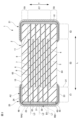

Classifications
-
- H—ELECTRICITY
- H01—ELECTRIC ELEMENTS
- H01G—CAPACITORS; CAPACITORS, RECTIFIERS, DETECTORS, SWITCHING DEVICES, LIGHT-SENSITIVE OR TEMPERATURE-SENSITIVE DEVICES OF THE ELECTROLYTIC TYPE
- H01G4/00—Fixed capacitors; Processes of their manufacture
- H01G4/002—Details
- H01G4/228—Terminals
- H01G4/232—Terminals electrically connecting two or more layers of a stacked or rolled capacitor
- H01G4/2325—Terminals electrically connecting two or more layers of a stacked or rolled capacitor characterised by the material of the terminals
-
- H—ELECTRICITY
- H01—ELECTRIC ELEMENTS
- H01G—CAPACITORS; CAPACITORS, RECTIFIERS, DETECTORS, SWITCHING DEVICES, LIGHT-SENSITIVE OR TEMPERATURE-SENSITIVE DEVICES OF THE ELECTROLYTIC TYPE
- H01G4/00—Fixed capacitors; Processes of their manufacture
- H01G4/002—Details
- H01G4/005—Electrodes
- H01G4/012—Form of non-self-supporting electrodes
-
- H—ELECTRICITY
- H01—ELECTRIC ELEMENTS
- H01G—CAPACITORS; CAPACITORS, RECTIFIERS, DETECTORS, SWITCHING DEVICES, LIGHT-SENSITIVE OR TEMPERATURE-SENSITIVE DEVICES OF THE ELECTROLYTIC TYPE
- H01G4/00—Fixed capacitors; Processes of their manufacture
- H01G4/002—Details
- H01G4/018—Dielectrics
- H01G4/06—Solid dielectrics
- H01G4/08—Inorganic dielectrics
- H01G4/12—Ceramic dielectrics
-
- H—ELECTRICITY
- H01—ELECTRIC ELEMENTS
- H01G—CAPACITORS; CAPACITORS, RECTIFIERS, DETECTORS, SWITCHING DEVICES, LIGHT-SENSITIVE OR TEMPERATURE-SENSITIVE DEVICES OF THE ELECTROLYTIC TYPE
- H01G4/00—Fixed capacitors; Processes of their manufacture
- H01G4/002—Details
- H01G4/228—Terminals
- H01G4/232—Terminals electrically connecting two or more layers of a stacked or rolled capacitor
-
- H—ELECTRICITY
- H01—ELECTRIC ELEMENTS
- H01G—CAPACITORS; CAPACITORS, RECTIFIERS, DETECTORS, SWITCHING DEVICES, LIGHT-SENSITIVE OR TEMPERATURE-SENSITIVE DEVICES OF THE ELECTROLYTIC TYPE
- H01G4/00—Fixed capacitors; Processes of their manufacture
- H01G4/30—Stacked capacitors
Definitions
- the present invention relates to a multilayer ceramic capacitor.
- the external electrodes of conventional multilayer ceramic capacitors are mainly composed of a Cu base electrode layer formed on the ceramic body, a Ni plating layer formed on the Cu base electrode layer, and a Sn plating layer formed on the Ni plating layer.
- the Ni plating layer and Sn plating layer are formed by electrolytic plating.
- the Ni plating layer formed on the Cu base electrode layer serves to prevent the Cu base electrode layer from dissolving into molten solder (solder erosion) when the multilayer ceramic capacitor is solder mounted on a substrate.
- the Cu base electrode layer formed on the ceramic body in the above-mentioned Patent Document 1 is formed by a dip method, a screen printing method, a roller coating method, or the like. Therefore, due to the characteristics of the printing method, the thickness of the Cu base electrode layer formed on the ridge line portion where any two of the main surface, side surface, or end surface of the ceramic body intersect may (possibly) be formed thinner than the surface area other than the ridge line portion.
- the Cu base electrode layer is formed thinly on the ridge line portion, the Cu base electrode layer is difficult to form continuously, and there are cases where a part of the ridge line portion is not covered with the Cu base electrode layer.
- the present invention aims to provide a multilayer ceramic capacitor that can suppress solder erosion that occurs on the ridge line portion of the ceramic body.
- the multilayer ceramic capacitor of the present invention comprises a laminate including a plurality of laminated dielectric layers and a plurality of internal electrode layers, the laminate having a first main surface and a second main surface facing each other in the lamination direction, a first side surface and a second side surface facing each other in a width direction perpendicular to the lamination direction, and a first end surface and a second end surface facing each other in a length direction perpendicular to the lamination direction and the width direction, and an external electrode provided on the first end surface and the second end surface, the external electrode being in contact with a Cu underlayer and covering the Cu underlayer.
- the laminate has a Ni plating layer and a Sn plating layer covering the Ni plating layer, and when the intersection of the two faces of the laminate is the ridgeline, the thickness of the Cu underlayer at the ridgeline of the laminate is smaller than the thickness of the Cu underlayer at the main face, the side face, and the end face, the coverage of the Cu underlayer at the ridgeline is 85% or more, and the difference between the coverage of the Cu underlayer at the ridgeline and the coverage of the Cu underlayer at the main face and the side face is within ⁇ 5%.
- the present invention provides a multilayer ceramic capacitor that can suppress solder erosion of the Cu underlayer.
- 1 is a perspective view of a multilayer ceramic capacitor according to an embodiment of the present invention
- 2 is a cross-sectional view taken along line YY in FIG. 1.
- 2 is a cross-sectional view taken along line XX in FIG. 1.
- Fig. 1 is a perspective view showing the multilayer ceramic capacitor 1 of the present embodiment.
- the multilayer ceramic capacitor 1 includes a laminate 2 and two external electrodes.
- the two external electrodes are a first external electrode 20 and a second external electrode 21.
- the L direction is the length direction L of the multilayer ceramic capacitor 1.
- the W direction is the width direction W of the multilayer ceramic capacitor 1.
- the T direction is the stacking direction T of the multilayer ceramic capacitor 1.
- the cross section shown in FIG. 2 is called an LT cross section.
- the cross section shown in FIG. 3 is called a WT cross section.
- the length direction L, the width direction W, and the stacking direction T do not necessarily have to be perpendicular to each other, but may intersect each other.
- the laminate 2 has a substantially rectangular parallelepiped shape.
- the laminate 2 has two end faces, two side faces, and two main faces.
- the end faces are faces facing the length direction L.
- the side faces are faces facing the width direction W.
- the main faces are faces facing the stacking direction T.
- the two end faces are a first end face 60 and a second end face 61.
- the two side faces are a first side face 62 and a second side face 63.
- the two main faces are a first main face 64 and a second main face 65.
- the first side face 62 and the second main face 65 are shown in FIG. 1.
- a portion where two faces intersect in the laminate 2 is defined as a ridge portion.
- a portion where three faces intersect in the laminate 2 is defined as a corner portion.
- a portion where the first main face 64 and the first side face 62 intersect is defined as a first longitudinal ridge portion 41
- a portion where the first main face 64 and the second side face 63 intersect is defined as a second longitudinal ridge portion 42
- a portion where the second main face 65 and the first side face 62 intersect is defined as a third longitudinal ridge portion 43
- a portion where the second main face 65 and the second side face 63 intersect is defined as a fourth longitudinal ridge portion 44.
- the portion where the first end face 60 and the first main surface 64 intersect is referred to as the first width direction ridge 45, and the portion where the first end face 60 and the second main surface 65 intersect is referred to as the second width direction ridge 46.
- the portion where the first end face 60 and the first side surface 62 intersect is referred to as the first height direction ridge 47, and the portion where the first end face 60 and the second side surface 63 intersect is referred to as the second height direction ridge 48.
- These ridges are not shown in FIG. 1, but are shown in FIG. 2 or FIG. 3.
- the ridges and corners of the laminate 2 are rounded.
- the size of the laminate 2 is not particularly limited.
- Fig. 2 is a cross-sectional view taken along line Y-Y in Fig. 1, showing the LT cross-section of the multilayer ceramic capacitor 1.
- the laminate 2 includes a plurality of dielectric layers and a plurality of internal electrode layers. The plurality of dielectric layers and the plurality of internal electrode layers are stacked on top of each other in the stacking direction T. Before describing the dielectric layers and the internal electrode layers, the divisions of the laminate 2 in the stacking direction T will be described. This is because the arrangement of the dielectric layers and the internal electrode layers differs depending on the division.
- the laminate 2 can be divided into an inner layer portion 57 and two outer layer portions in the stacking direction T.
- the two outer layer portions are a first outer layer portion 58 and a second outer layer portion 59.
- the first outer layer portion 58 and the second outer layer portion 59 are located at positions sandwiching the inner layer portion 57 in the stacking direction T.
- a plurality of dielectric layers and a plurality of internal electrode layers are arranged in the inner layer portion 57. Only dielectric layers are arranged in the first outer layer portion 58 and the second outer layer portion 59.
- the dielectric layer disposed in the inner layer portion 57 is referred to as an inner dielectric layer 4 .
- the internal electrode layers include a first internal electrode layer 6 and a second internal electrode layer 7.
- the first internal electrode layer 6 is an internal electrode layer connected to the first external electrode 20.
- the second internal electrode layer 7 is an internal electrode layer connected to the second external electrode 21.
- the first internal electrode layer 6 extends from a first end face 60 toward a second end face 61.
- the second internal electrode layer 7 extends from the second end face 61 toward the first end face 60.
- the inner layer portion 57 In the inner layer portion 57, the first internal electrode layer 6 and the second internal electrode layer 7 face each other via the inner dielectric layer 4. A capacitance is formed in the inner layer portion 57. Therefore, the inner layer portion 57 is the portion of the laminate 2 that essentially functions as a capacitor. For this reason, the inner layer portion 57 is also called the effective portion.
- the first outer layer portion 58 is the outer layer portion located on the side of the first main surface 64 of the laminate 2. Specifically, the first outer layer portion 58 is a portion between the first internal electrode layer 6 or the second internal electrode layer 7, which is closest to the first main surface 64, and the first main surface 64.
- the second outer layer portion 59 is the outer layer portion of the two outer layers that is located on the side of the second main surface 65 of the laminate 2. Specifically, the second outer layer portion 59 is the portion between the second main surface 65 and the first internal electrode layer 6 or the second internal electrode layer 7 that is closest to the second main surface 65, out of the first internal electrode layer 6 and the second internal electrode layer 7.
- No internal electrode layer is disposed on the first outer layer portion 58 and the second outer layer portion 59. Only a dielectric layer is disposed on the first outer layer portion 58 and the second outer layer portion 59. The dielectric layer disposed on the first outer layer portion 58 or the second outer layer portion 59 is referred to as the outer dielectric layer 5.
- the first outer layer portion 58 and the second outer layer portion 59 function as a protective layer for the inner layer portion 57.
- the total number of inner dielectric layers 4 and outer dielectric layers 5 laminated in the laminate 2 can be, for example, 5 to 2000.
- the material for the inner dielectric layer 4 and the outer dielectric layer 5 may be, for example, a dielectric ceramic composed mainly of BaTiO 3 , CaTiO 3 , SrTiO 3 , CaZrO 3 or the like.
- a material containing a sub-component such as a Mn compound, an Fe compound, a Cr compound, a Co compound, or a Ni compound added to the main component may also be used.
- each of the inner dielectric layer 4 or the outer dielectric layer 5 may be, for example, 0.3 ⁇ m or more and 0.6 ⁇ m or less.
- the first internal electrode layer 6 has a first opposing electrode portion 8 and a first lead electrode portion 10.
- the second internal electrode layer 7 has a second opposing electrode portion 9 and a second lead electrode portion 11.
- the first opposing electrode portion 8 is a portion of the first internal electrode layer 6 that faces the second internal electrode layer 7 in the stacking direction T.
- the second opposing electrode portion 9 is a portion of the second internal electrode layer 7 that faces the first internal electrode layer 6 in the stacking direction T.
- the first extension electrode portion 10 is a portion of the first internal electrode layer 6 that is extended from the first opposing electrode portion 8 to the first end surface 60 of the laminate 2.
- the second extension electrode portion 11 is a portion of the second internal electrode layer 7 that is extended from the second opposing electrode portion 9 to the second end surface 61 of the laminate 2.
- the division of the laminate 2 in the longitudinal direction L will be described.
- the laminate 2 can be divided in the longitudinal direction L into an L electrode opposing portion 50, a first L gap portion 51, and a second L gap portion 52.
- the L electrode opposing portion 50 corresponds to a portion where the first internal electrode layer 6 and the second internal electrode layer 7 oppose each other in the lamination direction T. A capacitance is formed in the L electrode opposing portion 50. For this reason, the L electrode opposing portion 50 is also called an effective portion.
- the first L gap 51 and the second L gap 52 are portions in the longitudinal direction L of the laminate 2 where the first internal electrode layer 6 and the second internal electrode layer 7 do not face each other in the stacking direction T.
- the first L gap 51 is a portion corresponding to between the L electrode opposing portion 50 and the first end face 60.
- the second L gap 52 is a portion corresponding to between the L electrode opposing portion 50 and the second end face 61.
- the first internal electrode layer 6 is arranged in the stacking direction T, but the second internal electrode layer 7 is not arranged.
- the second internal electrode layer 7 is arranged in the stacking direction T, but the first internal electrode layer 6 is not arranged.
- the first L gap 51 functions as an extension to the first end face 60 of the first opposing electrode portion 8.
- the second L gap 52 functions as an extension to the second end face 61 of the second opposing electrode portion 9.
- the length in the longitudinal direction L of each of the first L gap portion 51 and the second L gap portion 52 can be, for example, 10% to 30% of the length in the longitudinal direction L of the laminate 2.
- the length in the longitudinal direction L of each of the first L gap portion 51 and the second L gap portion 52 can be, for example, 5 ⁇ m to 30 ⁇ m.
- the total number of the first internal electrode layers 6 and the second internal electrode layers 7 can be, for example, 10 layers or more and 2000 layers or less.
- each of the first internal electrode layers 6 or the second internal electrode layers 7 can be, for example, 0.1 ⁇ m or more and 5.0 ⁇ m or less, and preferably 0.2 ⁇ m or more and 2.0 ⁇ m or less.
- the material of the first internal electrode layer 6 and the second internal electrode layer 7 can be, for example, metals such as Ni, Cu, Ag, Pd, and Au, alloys of Ni and Cu, alloys of Ag and Pd, etc.
- the material of the first internal electrode layer 6 and the second internal electrode layer 7 may additionally contain dielectric particles of the same composition as the ceramic contained in the inner dielectric layer 4 or the outer dielectric layer 5.
- the laminate 2 is provided with two external electrodes, a first external electrode 20 and a second external electrode 21.
- the first external electrode 20 is an external electrode that is mainly disposed on a first end surface 60 of the laminate 2.
- the first external electrode 20 is electrically connected to the first internal electrode layer 6.
- the second external electrode 21 is an external electrode that is mainly disposed on a second end surface 61 of the laminate 2.
- the second external electrode 21 is electrically connected to the second internal electrode layer 7.
- the first external electrode 20 extends from the first end face 60 to a portion of each of the first main face 64, the second main face 65, the first side face 62, and the second side face 63.
- the second external electrode 21 extends from the second end face 61 to a portion of each of the first main face 64, the second main face 65, the first side face 62, and the second side face 63.
- the first external electrode 20 on the first end face 60 is the first end face external electrode 22
- the first external electrode 20 on the first main face 64 is the first main face external electrode 23
- the first external electrode 20 on the second main face 65 is the second main face external electrode 24
- the first external electrode 20 on the first side face 62 is the first side face external electrode 25
- the first external electrode 20 on the second side face 63 is the second side face external electrode 26.
- FIG. 2 shows the first end face external electrode 22, the first main face external electrode 23, and the second main face external electrode 24.
- the other external electrodes are shown in FIG. 3.
- the second external electrode 21 is also similar to the first external electrode 20. A description of the second external electrode 21 is omitted.
- the layer structure of the external electrodes will be described with reference to Fig. 2.
- the layer structure of the first external electrode 20 is similar to that of the second external electrode 21.
- the layer structure of the external electrodes will be described using the first external electrode 20 as an example.
- the first external electrode 20 includes a Cu underlayer 30, a Ni plating layer 31, and a Sn plating layer 32. These layers are laminated in the order of the Cu underlayer 30, the Ni plating layer 31, and the Sn plating layer 32 from the first end surface 60 of the laminate 2, etc.
- the Cu underlayer 30 is disposed mainly on the first end face 60 of the laminate 2, covering the first end face 60.
- the Cu underlayer 30 extends from the first end face 60 to a part of the first main surface 64, a part of the second main surface 65, a part of the first side surface 62, and a part of the second side surface 63.
- the Cu underlayer 30 is a layer containing metal and glass components.
- the metal includes at least one selected from the group consisting of Cu, Ni, Ag, Pd, Ag-Pd alloy, and Au.
- the glass component includes at least one selected from the group consisting of B, Si, Ba, Mg, Al, and Li.
- the thickness of the Cu underlayer 30 at the ridgeline is smaller than the thickness of the Cu underlayer 30 on the main surface, side surfaces, and end surfaces.
- the thickness of the Cu underlayer 30 is preferably 10 ⁇ m or more, particularly at the ridgeline.
- the Ni plating layer 31 is a plating layer provided so as to cover the Cu underlayer 30.
- the Ni plating layer 31 is also called an inner plating layer.
- solder is used.
- the Ni plating layer 31 can suppress the Cu underlayer 30 from being eroded by solder due to solder eating, which will be described later.
- the Ni plating layer 31 is formed with a substantially uniform thickness relative to the Cu underlayer 30.
- the ratio of the thickness of the Ni plating layer 31 to the thickness of the Cu underlayer 30 at the ridgeline portion i.e., the thickness of the Ni plating layer 31/the thickness of the Cu underlayer 30, is greater than the ratio of the thickness of the Ni plating layer 31 to the thickness of the Cu underlayer 30 at the main surface, side surface, and end surface. This is because the thickness of the Cu underlayer 30 at the ridgeline portion is smaller than the thickness of the Cu underlayer 30 at the main surface, side surface, and end surface.
- the thickness of the Ni plating layer 31 is 2.0 ⁇ m or more, especially at the ridgeline. This ensures that the Ni plating layer 31 is sufficiently thick at the ridgeline, where the thickness of the Cu underlayer 30 is relatively small compared to other surfaces. This further suppresses the occurrence of solder erosion.
- the Sn plating layer 32 is a plating layer provided so as to cover the Ni plating layer 31.
- the Sn plating layer 32 is also called an outer plating layer.
- the Sn plating layer 32 can improve the wettability of the solder when mounting the multilayer ceramic capacitor 1. This can facilitate mounting of the multilayer ceramic capacitor 1.
- the thickness of the Ni plating layer 31 and the Sn plating layer 32 is preferably, for example, 2.0 ⁇ m or more. By making the thickness of the Ni plating layer 2.0 ⁇ m or more, the Cu underlayer 30 can be further prevented from being eroded by the solder.
- Fig. 3 is a WT cross-sectional view of the multilayer ceramic capacitor 1.
- the laminate 2 can be divided in the width direction W into a W electrode opposing portion 54, a first W gap portion 55, and a second W gap portion 56.
- the W electrode opposing portion 54 corresponds to a portion where the first internal electrode layer 6 and the second internal electrode layer 7 oppose each other in the stacking direction T. A capacitance is formed in the W electrode opposing portion 54. For this reason, the W electrode opposing portion 54 is also called an effective portion.
- the first W gap 55 and the second W gap 56 are portions in which neither the first internal electrode layer 6 nor the second internal electrode layer 7 is arranged in the width direction W of the laminate 2.
- the first W gap 55 is a portion between the W electrode opposing portion 54 and the first side surface 62 in the width direction W of the laminate 2.
- the second W gap 56 is a portion between the W electrode opposing portion 54 and the second side surface 63 in the width direction W of the laminate 2.
- the first W gap portion 55 and the second W gap portion 56 are arranged to sandwich the W electrode opposing portion 54.
- the first W gap portion 55 and the second W gap portion 56 function as protective layers for the first internal electrode layer 6 and the second internal electrode layer 7.
- the length in the width direction W of each of the first W gap portion 55 and the second W gap portion 56 can be, for example, 20% to 30% of the length in the width direction W of the laminate 2.
- the length in the width direction W of each of the first W gap portion 55 and the second W gap portion 56 can be, for example, 5 ⁇ m to 50 ⁇ m.
- the size of the multilayer ceramic capacitor 1 is not particularly limited.
- the size of the multilayer ceramic capacitor 1 can be, for example, as follows.
- the dimension in the length direction L of the multilayer ceramic capacitor 1 including the laminate 2 and the external electrodes is defined as the L dimension.
- the L dimension is preferably 0.25 mm or more and 1.0 mm or less.
- the dimension in the stacking direction T of the multilayer ceramic capacitor 1 including the laminate 2 and the external electrodes is defined as the T dimension.
- the T dimension is preferably 0.125 mm or more and 0.5 mm or less.
- the dimension in the width direction W of the multilayer ceramic capacitor 1 including the laminate 2 and the external electrodes is defined as the W dimension.
- the W dimension is preferably 0.125 mm or more and 0.5 mm or less.
- the lengths of each part of the laminate 2 and the external electrodes can be measured with a micrometer or an optical microscope.
- the multilayer ceramic capacitor 1 has been described as a two-terminal multilayer ceramic capacitor as an example.
- the multilayer ceramic capacitor 1 is not limited to being a two-terminal multilayer ceramic capacitor.
- the multilayer ceramic capacitor 1 may also be a multi-terminal multilayer ceramic capacitor having three or more terminals.
- the multilayer ceramic capacitor 1 of this embodiment is characterized by the coverage rate of the Cu underlayer 30. Furthermore, the multilayer ceramic capacitor 1 of this embodiment can suppress solder erosion of the Cu underlayer 30 by simple means.
- solder eaten Solder erosion will now be described.
- the heat generated during soldering can cause Sn contained in the solder to react with Cu contained in an electrode layer containing Cu formed on an end face of the multilayer ceramic capacitor 1, for example, Cu contained in a Cu underlayer, to produce a CuSn compound.
- This reaction between Sn contained in the solder and Cu in the electrode layer containing Cu is called solder erosion.
- solder erosion can impair the reliability of the electrical connection between the internal electrodes of the multilayer ceramic capacitor 1 and the electrode layer containing Cu.
- the inventors have found that when the coverage of the Cu underlayer 30 is poor, the ceramic body is prone to deterioration due to the temperature during solder mounting, and the Cu underlayer 30 is prone to solder erosion. The inventors have also found that the coverage of the Cu underlayer 30 tends to be poorer at the ridges than in other parts of the laminate 2.
- the thickness of the Cu underlayer 30 is small at the ridges and large on the main surfaces and side surfaces.
- the coverage of the Cu underlayer 30 at the ridges is 85% or more.
- the difference between the coverage of the Cu underlayer 30 at the ridges and the coverage of the Cu underlayer 30 on the main surfaces and side surfaces is within ⁇ 5%.
- the region other than the metal region means a region occupied by voids or glass or the like.
- the metal region and the region other than the metal can be determined, for example, by exposing the region by polishing or the like as necessary and observing the cross section with an optical microscope or the like.
- This embodiment is characterized by the coverage of the Cu underlayer 30. Therefore, in the following description, unless otherwise specified, coverage refers to the coverage of the Cu underlayer 30.
- the coverage rates in the following five areas will be explained.
- the five areas are the coverage rate A1 of the longitudinal ridgeline, the coverage rate A2 of the widthwise ridgeline, the coverage rate B1 of the end faces, the coverage rate B2 of the side faces, and the coverage rate B3 of the main faces, as shown in Figure 1.
- the calculation area of the coverage will be described. First, the coverage A1 of the longitudinal ridgeline, the coverage B2 of the side surface, and the coverage B3 of the main surface will be described based on the WT cross-sectional view. In FIG. 3, the calculation area of the coverage A1 of the longitudinal ridgeline, the coverage B2 of the side surface, and the coverage B3 of the main surface are shown in dotted lines. These calculation areas are determined based on the division lines when the laminate 2 is divided into four. In FIG. 3, the division lines when the WT cross-section of the laminate 2 is divided into four in the stacking direction T and the width direction W are shown. The division lines when the laminate 2 is divided into four in the stacking direction T are shown as division lines L1 to L3. Also, the division lines when the laminate 2 is divided into four in the width direction W are shown as division lines L5 to L7.
- the calculation area of the coverage rate A1 of the longitudinal ridgeline portion will be described using the third longitudinal ridgeline portion 43 as an example.
- the calculation area of the coverage rate A1 of the longitudinal ridgeline portion is set as the calculation area RA1.
- the calculation area RA1 is a part including the Cu underlayer 30 included in the area where the third longitudinal ridgeline portion 43 exists among the four areas divided by the division lines L3 and L5. This calculation area RA1 includes the Cu underlayer 30 in the vicinity of the third longitudinal ridgeline portion 43.
- the Cu underlayer 30 near the first longitudinal ridge 41 is the calculation region RA1.
- the Cu underlayer 30 near the second longitudinal ridge 42 is the calculation region RA1.
- the Cu underlayer 30 near the fourth longitudinal ridge 44 is the calculation region RA1.
- the side coverage B2 will be described using the first side 62 as an example.
- the calculation region for the side coverage B2 is set as calculation region RB2.
- Calculation region RB2 is a portion including the Cu underlayer 30 on the first side 62 included in the region divided by division lines L1 and L3. This calculation region RB2 includes the Cu underlayer 30 in the vicinity of the first height direction ridge portion 47 and in the central portion of the first side 62 in the stacking direction T.
- the portion including the Cu underlayer 30 on the second side 63 included in the area divided by the division lines L1 and L3 becomes the calculation region RB2.
- the coverage rate B3 of the main surface will be described using the second main surface 65 as an example.
- the calculation region of the coverage rate B3 of the main surface is defined as calculation region RB3.
- the calculation region RB3 is a portion including the Cu underlayer 30 on the second main surface 65 included in the region divided by the division lines L5 and L7.
- This calculation region RB3 includes the Cu underlayer 30 in the vicinity of the second width direction ridge portion 46 and in the central portion of the second main surface 65 in the width direction W.
- the portion including the Cu underlayer 30 on the first principal surface 64 included in the region divided by the division lines L5 and L7 is the calculation region RB3.
- the coverage rate A1 of the longitudinal ridgeline portion is 85% or more.
- the coverage rate A1 of the longitudinal ridgeline portion is 95% or more.
- the difference between the coverage rate A1 of the longitudinal ridgeline portion and the coverage rate B2 of the side surface is within ⁇ 5% of the coverage rate A1 of the longitudinal ridgeline portion.
- the difference between the coverage rate A1 of the longitudinal ridgeline portion and the coverage rate B3 of the main surface is within ⁇ 5% of the coverage rate A1 of the longitudinal ridgeline portion.
- the side coverage B2 and the main surface coverage B3 are equal or substantially equal to the longitudinal ridge coverage A1.
- substantially equal means, for example, that the difference is within the margin of error and that they perform similar functions.
- the preferred coverage rate explained above can be written as a formula: 85%, preferably 95% ⁇ A1 ⁇ B2, B3.
- Fig. 2 shows the calculation area for the coverage rate A2 of the width direction ridgeline and the coverage rate B1 of the end face.
- These calculation regions are determined based on the dividing lines L1 to L3 when the laminate 2 is divided into four in the stacking direction T, and the boundary line between the L electrode opposing portion 50 and the first L gap portion 51.
- the boundary line between the L electrode opposing portion 50 and the first L gap portion 51 is boundary line L4.
- the dividing lines L1 to L3 are the same as the dividing lines L1 to L3 shown in FIG. 3 above.
- the calculation area of the coverage rate A2 of the width direction ridgeline portion will be described using the second width direction ridgeline portion 46 as an example.
- the calculation area of the coverage rate A2 of the width direction ridgeline portion is set as calculation area RA2.
- the calculation area RA2 is a part including the Cu underlayer 30 included in the area where the second width direction ridgeline portion 46 exists, among the four areas divided by the division line L3 and the boundary line L4.
- This calculation area RA2 includes the Cu underlayer 30 in the vicinity of the second width direction ridgeline portion 46.
- the Cu underlayer 30 near the first width direction ridge portion 45 which is included in the area divided by the division line L1 and the boundary line L4, becomes the calculation area RA2.
- the end face coverage B1 will be described using the first end face 60 as an example.
- the calculation region for the end face coverage B1 is set as calculation region RB1.
- Calculation region RB1 is a portion including the Cu underlayer 30 on the first end face 60 included in the region divided by parting line L1 and parting line L3. This calculation region RB1 includes the Cu underlayer 30 in the center of the first end face 60 in the stacking direction T.
- the portion including the Cu underlayer 30 on the second end face 61 included in the section separated by the division line L1 and the division line L3 becomes the calculation region RB1.
- the coverage rate A2 of the width direction ridgeline is 85% or more.
- the coverage rate A2 of the width direction ridgeline is 95% or more.
- the difference between the coverage rate A2 of the widthwise ridgeline portion and the coverage rate B1 of the end face is within ⁇ 5% of the coverage rate A2 of the widthwise ridgeline portion. Even more preferably, the coverage rate B1 of the end face is equal to or substantially equal to the coverage rate A2 of the widthwise ridgeline portion.
- the coverage rate B1 of the end face is equal to or substantially equal to the coverage rate B3 of the main face.
- the coverage rate of the Cu underlayer 30 is uniform on the first main face 64, the second main face 65, the first end face 60, the first width direction ridge portion 45, and the second width direction ridge portion 46.
- the above-mentioned preferred coverage rate can be written as a formula: 85%, preferably 95% ⁇ A2 ⁇ B1, B3.
- the coverage rate A1 of the longitudinal ridgeline portion, the coverage rate A2 of the widthwise ridgeline portion, the coverage rate B1 of the end faces, the coverage rate B2 of the side faces, and the coverage rate B3 of the main faces are all 85% or more, or even 95% or more.
- the coverage rate A1 of the longitudinal ridgeline portion, the coverage rate A2 of the widthwise ridgeline portion, the coverage rate B1 of the end face, the coverage rate B2 of the side face, and the coverage rate B3 of the main face are equal or substantially equal.
- the above preferred embodiment can be written as a formula: 85% preferably 95% ⁇ A1 ⁇ B1, B2, B3, or 85% preferably 95% ⁇ A2 ⁇ B1, B2, B3.
- the electrode paste is applied to the ceramic green sheets in a desired pattern by, for example, screen printing or gravure printing.
- a predetermined number of ceramic green sheets without a printed pattern of the internal electrode layer are stacked. This creates a portion that corresponds to the outer layer portion.
- ceramic green sheets for the inner layer portion coated with paste are stacked in order. This creates a portion that corresponds to the inner layer portion 57.
- a predetermined number of ceramic green sheets for the other outer layer portion are stacked. This creates a laminated sheet. The laminated sheet is pressed in the stacking direction by means of a hydrostatic press or the like to create a laminated block.
- the laminated block is cut to a predetermined size to cut out laminated chips. At this time, corners and edges of the laminated chips may be rounded by barrel polishing or the like.
- the laminated chip is fired to produce the laminate 2.
- the firing temperature depends on the materials of the dielectric layers and the internal electrode layers, but is preferably 900° C. or higher and 1400° C. or lower.
- the external electrodes include a Cu underlayer 30, a Ni plating layer 31, and a Sn plating layer 32.
- a conductive paste that will become the Cu underlayer 30 is applied to two end faces of the laminate 2 and baked to form the Cu underlayer 30. Specifically, a conductive paste containing a glass component and a metal is applied to the laminate 2 by a method such as dipping. After application, a baking process is performed to form the Cu underlayer 30.
- the baking process temperature is preferably 500° C. or higher and 900° C. or lower.
- the baking process time is preferably 30 minutes or higher and 2 hours or lower.
- the baking process atmosphere is preferably a reducing atmosphere containing, for example, H 2 O or H 2 .
- Method to make the coverage uniform An example of a method for making the coverage of the Cu underlayer 30 at each portion uniform as described above will be described.
- the multilayer ceramic capacitor 1 on which the Cu underlayer 30 is formed and before the Ni plating layer 31 is formed is used as a pre-plating intermediate body.
- the pre-plating intermediate body is placed in a container, the container is rotated, and particles are sprayed into the rotating container. This polishes the Cu underlayer 30, making it possible to make the coverage of the Cu underlayer 30 uniform.
- a specific description will be given below.
- the coverage rate of the Cu underlayer 30 on the ridgeline portion of the pre-plating intermediate body may be smaller than the coverage rate of the Cu underlayer 30 on the other portions of the ridgeline portion. In this case, the coverage rate of the Cu underlayer 30 can be made uniform by improving the coverage rate of the Cu underlayer 30 on the ridgeline portion.
- the container containing the pre-plating intermediate is rotated and sandblasted by spraying fine particles made of materials such as zirconia or alumina. This allows the blasting material, i.e., the fine particles, to collide preferentially with the ridgeline. This collision causes the Cu underlayer 30 on the ridgeline to be stretched by the sandblasting due to its ductility. This improves the coverage of the Cu underlayer 30 on the ridgeline. As a result, the coverage of the Cu underlayer 30 on the ridgeline approaches the coverage of the Cu underlayer 30 outside the ridgeline. In this way, the coverage of the Cu underlayer 30 is made uniform.
- the above process can be described as a Cu underlayer polishing method step by step as follows. That is, the Cu underlayer polishing method includes the steps of putting a pre-plating intermediate body, in which a Cu underlayer 30 as part of an external electrode is formed on the laminate 2, into a container, rotating the container, and spraying particles into the rotating container.
- Ni plating layer 31 is formed on the surface of the Cu underlayer 30.
- the Ni plating layer 31 is formed by, for example, barrel plating.
- the Sn plating layer 32 is formed on the Ni plating layer 31.
- the Sn plating layer 32 is formed by, for example, barrel plating.
- the dimensions and thicknesses of each part can be determined, if necessary, by polishing a cross section of the multilayer ceramic capacitor 1 or the laminate 2 and measuring it using a digital microscope or the like.
- the multilayer ceramic capacitor 1 of this embodiment was mounted on a printed wiring board by solder bonding, and then the presence or absence of solder erosion was evaluated by observing a cross section of the multilayer ceramic capacitor 1. In the multilayer ceramic capacitor 1 of this embodiment, no solder erosion occurred even due to the heat during solder bonding.
Landscapes
- Engineering & Computer Science (AREA)
- Power Engineering (AREA)
- Manufacturing & Machinery (AREA)
- Microelectronics & Electronic Packaging (AREA)
- Chemical & Material Sciences (AREA)
- Ceramic Engineering (AREA)
- Inorganic Chemistry (AREA)
- Fixed Capacitors And Capacitor Manufacturing Machines (AREA)
- Ceramic Capacitors (AREA)
Abstract
Cu下地層の半田食われを抑制することが可能な積層セラミックコンデンサを提供することを提供すること。積層セラミックコンデンサ1は、積層体2と、第1の端面60及び第2の端面61に設けられた外部電極とを備え、外部電極は、Cu下地層30と、Cu下地層30に接触してCu下地層30を覆うNiめっき層31と、Niめっき層31を覆うSnめっき層32を有し、積層体2の2つの面が交わる部分を稜線部としたとき、積層体2の稜線部におけるCu下地層30の厚さは、主面、側面及び端面におけるCu下地層30の厚さよりも小さく、稜線部におけるCu下地層30の被覆率は85%以上であり、稜線部におけるCu下地層30の被覆率と、主面及び側面におけるCu下地層30の被覆率との差は、±5%以内である。
Description
本発明は、積層セラミックコンデンサに関する。
従来の積層セラミックコンデンサの外部電極は、主にセラミック素体の上に形成されたCu下地電極層、Cu下地電極層上に形成されたNiめっき層、Niめっき層の上に形成されたSnめっき層により構成されている。一般的に、Niめっき層、Snめっき層は、電界めっき法(電気めっき法)によって形成される。Cu下地電極層上に形成されたNiめっき層は、積層セラミックコンデンサを基板上に半田実装する際、Cu下地電極層が溶融半田中に溶けだしてしまうこと(はんだ食われ)を防止する役割をもっている。
上記特許文献1におけるセラミック素体の上に形成されたCu下地電極層は、ディップ法またはスクリーン印刷法またはローラ塗布法などにより形成されている。そのため、印刷法の特性上、セラミック素体の主面、側面、端面のいずれか2面が交わる稜線部に形成されるCu下地電極層の厚さは、稜線部以外の面領域よりも薄く形成されることがある(可能性がある)。稜線部では、Cu下地電極層は薄く形成されているとき、Cu下地電極層が連続して形成されにくく、稜線部の一部において、Cu下地電極層で覆われていない箇所が発生する場合があった。Cu下地電極層上に形成されるNiめっき層は、電界めっき法によって形成されるため、稜線部の一部において、金属であるCu下地電極層が形成されていない箇所に、Niめっき層が形成されない。そのため、Cu下地電極層のはんだ食われを防止することができない問題があった。そこで、本発明は、セラミック素体の稜線部で発生するはんだ食われを抑制することが可能な積層セラミックコンデンサを提供することを課題とする。
本発明の積層セラミックコンデンサは、積層された複数の誘電体層と複数の内部電極層とを含み、積層方向に相対する第1の主面及び第2の主面と、積層方向に直交する幅方向に相対する第1の側面及び第2の側面と、積層方向及び幅方向に直交する長さ方向に相対する第1の端面及び第2の端面とを備える積層体と、前記第1の端面及び第2の端面に設けられた外部電極とを備え、前記外部電極は、Cu下地層と、前記Cu下地層に接触して前記Cu下地層を覆うNiめっき層と、前記Niめっき層を覆うSnめっき層を有し、前記積層体の2つの面が交わる部分を稜線部としたとき、前記積層体の前記稜線部における前記Cu下地層の厚さは、前記主面、前記側面及び前記端面における前記Cu下地層の厚さよりも小さく、前記稜線部における前記Cu下地層の被覆率は85%以上であり、前記稜線部における前記Cu下地層の被覆率と、前記主面及び前記側面における前記Cu下地層の被覆率との差は、±5%以内である。
本発明によれば、Cu下地層の半田食われを抑制することが可能な積層セラミックコンデンサを提供することができる。
(積層セラミックコンデンサの外形)
図1に基づいて、積層セラミックコンデンサ1の外観の概要を説明する。図1は、本実施形態の積層セラミックコンデンサ1を示す斜視図である。積層セラミックコンデンサ1は、積層体2及び2つの外部電極を備える。2つの外部電極は、第1の外部電極20及び第2の外部電極21である。
図1に基づいて、積層セラミックコンデンサ1の外観の概要を説明する。図1は、本実施形態の積層セラミックコンデンサ1を示す斜視図である。積層セラミックコンデンサ1は、積層体2及び2つの外部電極を備える。2つの外部電極は、第1の外部電極20及び第2の外部電極21である。
(方向の定義)
図面には、適宜、L方向、W方向及びT方向が示されている。L方向は、積層セラミックコンデンサ1の長さ方向Lである。W方向は、積層セラミックコンデンサ1の幅方向Wである。T方向は、積層セラミックコンデンサ1の積層方向Tである。これにより、図2に示す断面はLT断面という。また、図3に示す断面はWT断面という。長さ方向L、幅方向W及び積層方向Tは、必ずしも互いに直交する関係でなく、互いに交差する関係であればよい。
図面には、適宜、L方向、W方向及びT方向が示されている。L方向は、積層セラミックコンデンサ1の長さ方向Lである。W方向は、積層セラミックコンデンサ1の幅方向Wである。T方向は、積層セラミックコンデンサ1の積層方向Tである。これにより、図2に示す断面はLT断面という。また、図3に示す断面はWT断面という。長さ方向L、幅方向W及び積層方向Tは、必ずしも互いに直交する関係でなく、互いに交差する関係であればよい。
(積層体の外形)
積層体2は、略直方体型の形状を有する。積層体2は、2つの端面、2つの側面及び2つの主面を有する。端面は、長さ方向Lに対向する面である。側面は、幅方向Wに対向する面である。主面は、積層方向Tに対向する面である。2つの端面は、第1の端面60及び第2の端面61である。2つの側面は、第1の側面62及び第2の側面63である。2つの主面は、第1の主面64及び第2の主面65である。図1には第1の側面62及び第2の主面65が示されている。
積層体2は、略直方体型の形状を有する。積層体2は、2つの端面、2つの側面及び2つの主面を有する。端面は、長さ方向Lに対向する面である。側面は、幅方向Wに対向する面である。主面は、積層方向Tに対向する面である。2つの端面は、第1の端面60及び第2の端面61である。2つの側面は、第1の側面62及び第2の側面63である。2つの主面は、第1の主面64及び第2の主面65である。図1には第1の側面62及び第2の主面65が示されている。
(稜線部)
積層体2において2面が交わる部分を稜線部とする。積層体2の3面が交る部分を角部とする。稜線部のうち、第1の主面64と第1の側面62とが交わる部分を第1の長さ方向稜線部41とし、第1の主面64と第2の側面63とが交わる部分を第2の長さ方向稜線部42とし、第2の主面65と第1の側面62とが交わる部分を第3の長さ方向稜線部43とし、第2の主面65と第2の側面63とが交わる部分を第4の長さ方向稜線部44とする。
積層体2において2面が交わる部分を稜線部とする。積層体2の3面が交る部分を角部とする。稜線部のうち、第1の主面64と第1の側面62とが交わる部分を第1の長さ方向稜線部41とし、第1の主面64と第2の側面63とが交わる部分を第2の長さ方向稜線部42とし、第2の主面65と第1の側面62とが交わる部分を第3の長さ方向稜線部43とし、第2の主面65と第2の側面63とが交わる部分を第4の長さ方向稜線部44とする。
さらに、稜線部のうち、第1の端面60と第1の主面64とが交わる部分を第1の幅方向稜線部45とし、第1の端面60と第2の主面65とが交わる部分を第2の幅方向稜線部46とする。また、第1の端面60と第1の側面62とが交わる部分を第1の高さ方向稜線部47とし、第1の端面60と第2の側面63とが交わる部分を第2の高さ方向稜線部48とする。これらの稜線部は図1には示されておらず、図2又は図3に示されている。
また、積層体2の稜線部及び角部には、丸みがつけられていることが好ましい。なお、積層体2の大きさは特には限定されない。
(積層体の内部構造(LT断面))
積層体2の断面図を参照しながら、積層体2の構造を説明する。図2は、図1のY-Y線断面図であり、積層セラミックコンデンサ1のLT断面を示す。積層体2は、複数の誘電体層及び複数の内部電極層を含む。複数の誘電体層及び複数の内部電極層は、互いに積層方向Tに積層されている。誘電体層及び内部電極層を説明する前に、積層体2の積層方向Tにおける区分について説明する。区分によって、誘電体層及び内部電極層の配置が異なるためである。
積層体2の断面図を参照しながら、積層体2の構造を説明する。図2は、図1のY-Y線断面図であり、積層セラミックコンデンサ1のLT断面を示す。積層体2は、複数の誘電体層及び複数の内部電極層を含む。複数の誘電体層及び複数の内部電極層は、互いに積層方向Tに積層されている。誘電体層及び内部電極層を説明する前に、積層体2の積層方向Tにおける区分について説明する。区分によって、誘電体層及び内部電極層の配置が異なるためである。
(内層部と外層部)
積層体2は、積層方向Tにおいて、内層部57及び2つの外層部に区分することができる。2つの外層部は、第1の外層部58及び第2の外層部59である。第1の外層部58及び第2の外層部59は、内層部57を積層方向Tにおいて挟む位置に位置している。内層部57には、複数の誘電体層及び複数の内部電極層が配置されている。第1の外層部58及び第2の外層部59には、誘電体層のみが配置されている。
積層体2は、積層方向Tにおいて、内層部57及び2つの外層部に区分することができる。2つの外層部は、第1の外層部58及び第2の外層部59である。第1の外層部58及び第2の外層部59は、内層部57を積層方向Tにおいて挟む位置に位置している。内層部57には、複数の誘電体層及び複数の内部電極層が配置されている。第1の外層部58及び第2の外層部59には、誘電体層のみが配置されている。
(内層誘電体層)
内層部57に配置されている誘電体層を内層誘電体層4とする。
内層部57に配置されている誘電体層を内層誘電体層4とする。
(内部電極層)
内部電極層は、第1の内部電極層6及び第2の内部電極層7を含む。第1の内部電極層6は、第1の外部電極20に接続された内部電極層である。第2の内部電極層7は、第2の外部電極21に接続された内部電極層である。第1の内部電極層6は、第1の端面60から、第2の端面61に向かって延在する。第2の内部電極層7は、第2の端面61から、第1の端面60に向かって延在する。
内部電極層は、第1の内部電極層6及び第2の内部電極層7を含む。第1の内部電極層6は、第1の外部電極20に接続された内部電極層である。第2の内部電極層7は、第2の外部電極21に接続された内部電極層である。第1の内部電極層6は、第1の端面60から、第2の端面61に向かって延在する。第2の内部電極層7は、第2の端面61から、第1の端面60に向かって延在する。
内層部57では、第1の内部電極層6と第2の内部電極層7とが内層誘電体層4を介して対向している。内層部57には、静電容量が形成される。そのため、内層部57は、積層体2のなかで実質的にコンデンサとして機能する部分である。これより、内層部57は、有効部ともいわれる。
(外層部)
第1の外層部58は、2つの外層部のうちで、積層体2の第1の主面64の側に位置する外層部である。具体的には、第1の外層部58は、第1の内部電極層6及び第2の内部電極層7のうち、第1の主面64に最も近い第1の内部電極層6又は第2の内部電極層7と、第1の主面64との間の部分である。
第1の外層部58は、2つの外層部のうちで、積層体2の第1の主面64の側に位置する外層部である。具体的には、第1の外層部58は、第1の内部電極層6及び第2の内部電極層7のうち、第1の主面64に最も近い第1の内部電極層6又は第2の内部電極層7と、第1の主面64との間の部分である。
第2の外層部59は、2つの外層部のうちで、積層体2の第2の主面65の側に位置する外層部である。具体的には、第2の外層部59は、第1の内部電極層6及び第2の内部電極層7のうち第2の主面65に最も近い第1の内部電極層6又は第2の内部電極層7と、第2の主面65との間の部分である。
第1の外層部58及び第2の外層部59には、内部電極層は配置されていない。第1の外層部58及び第2の外層部59には、誘電体層のみが配置されている。第1の外層部58又は第2の外層部59に配置されている誘電体層を外層誘電体層5とする。第1の外層部58及び第2の外層部59は、内層部57の保護層として機能する。
(誘電体層の層数)
積層体2に積層される内層誘電体層4及び外層誘電体層5の合計の層数は、例えば、5層以上2000層以下とすることができる。
積層体2に積層される内層誘電体層4及び外層誘電体層5の合計の層数は、例えば、5層以上2000層以下とすることができる。
(誘電体層の材料)
内層誘電体層4及び外層誘電体層5の材料としては、例えば、BaTiO3、CaTiO3、SrTiO3、CaZrO3などの主成分からなる誘電体セラミックを用いることができる。また、これらの主成分にMn化合物、Fe化合物、Cr化合物、Co化合物、Ni化合物などの副成分を添加したものを用いてもよい。
内層誘電体層4及び外層誘電体層5の材料としては、例えば、BaTiO3、CaTiO3、SrTiO3、CaZrO3などの主成分からなる誘電体セラミックを用いることができる。また、これらの主成分にMn化合物、Fe化合物、Cr化合物、Co化合物、Ni化合物などの副成分を添加したものを用いてもよい。
(誘電体層の厚さ)
内層誘電体層4又は外層誘電体層5の一層の厚さは、例えば、0.3μm以上0.6μm以下とすることができる。
内層誘電体層4又は外層誘電体層5の一層の厚さは、例えば、0.3μm以上0.6μm以下とすることができる。
(対向部と引き出し部)
第1の内部電極層6は、第1の対向電極部8及び第1の引き出し電極部10を有する。また、第2の内部電極層7は、第2の対向電極部9及び第2の引き出し電極部11を有する。第1の対向電極部8は、第1の内部電極層6のなかで、第2の内部電極層7と積層方向Tにおいて対向する部分である。第2の対向電極部9は、第2の内部電極層7のなかで、第1の内部電極層6と積層方向Tにおいて対向する部分である。
第1の内部電極層6は、第1の対向電極部8及び第1の引き出し電極部10を有する。また、第2の内部電極層7は、第2の対向電極部9及び第2の引き出し電極部11を有する。第1の対向電極部8は、第1の内部電極層6のなかで、第2の内部電極層7と積層方向Tにおいて対向する部分である。第2の対向電極部9は、第2の内部電極層7のなかで、第1の内部電極層6と積層方向Tにおいて対向する部分である。
第1の引き出し電極部10は、第1の内部電極層6のなかで、第1の対向電極部8から、積層体2の第1の端面60まで引き出された部分である。第2の引き出し電極部11は、第2の内部電極層7のなかで、第2の対向電極部9から、積層体2の第2の端面61まで引き出された部分である。
(L電極対向部)
積層体2の長さ方向Lの区分について説明する。積層体2は、長さ方向Lにおいて、L電極対向部50、第1のLギャップ部51及び第2のLギャップ部52に区分することができる。L電極対向部50は、第1の内部電極層6と第2の内部電極層7とが積層方向Tにおいて対向する部分に対応する。L電極対向部50には容量が形成される。これより、L電極対向部50は、有効部ともいわれる。
積層体2の長さ方向Lの区分について説明する。積層体2は、長さ方向Lにおいて、L電極対向部50、第1のLギャップ部51及び第2のLギャップ部52に区分することができる。L電極対向部50は、第1の内部電極層6と第2の内部電極層7とが積層方向Tにおいて対向する部分に対応する。L電極対向部50には容量が形成される。これより、L電極対向部50は、有効部ともいわれる。
(Lギャップ部)
第1のLギャップ部51及び第2のLギャップ部52は、積層体2の長さ方向Lにおいて、第1の内部電極層6と第2の内部電極層7とが積層方向Tに対向しない部分である。第1のLギャップ部51は、L電極対向部50と第1の端面60との間に対応する部分である。第2のLギャップ部52は、L電極対向部50と第2の端面61とのに対応する部分である。
第1のLギャップ部51及び第2のLギャップ部52は、積層体2の長さ方向Lにおいて、第1の内部電極層6と第2の内部電極層7とが積層方向Tに対向しない部分である。第1のLギャップ部51は、L電極対向部50と第1の端面60との間に対応する部分である。第2のLギャップ部52は、L電極対向部50と第2の端面61とのに対応する部分である。
第1のLギャップ部51においては、積層方向Tに、第1の内部電極層6は配置されているが、第2の内部電極層7は配置されていない。第2のLギャップ部52においては、積層方向Tに、第2の内部電極層7は配置されているが、第1の内部電極層6は配置されていない。第1のLギャップ部51は、第1の対向電極部8の第1の端面60への引出部として機能する。第2のLギャップ部52は、第2の対向電極部9の第2の端面61への引出部として機能する。
第1のLギャップ部51及び第2のLギャップ部52のそれぞれの長さ方向Lの長さは、例えば、積層体2の長さ方向Lの長さの10%以上30%以下とすることができる。また、第1のLギャップ部51及び第2のLギャップ部52のそれぞれの長さ方向Lの長さは、例えば、5μm以上30μm以下とすることができる。
(内部電極層の層数)
第1の内部電極層6及び第2の内部電極層7の合計層数は、例えば、10層以上2000層以下とすることができる。
第1の内部電極層6及び第2の内部電極層7の合計層数は、例えば、10層以上2000層以下とすることができる。
(内部電極層の厚さ)
第1の内部電極層6又は第2の内部電極層7の一層の厚さは、例えば、0.1μm以上5.0μm以下、好ましくは、0.2μm以上2.0μm以下とすることができる。
第1の内部電極層6又は第2の内部電極層7の一層の厚さは、例えば、0.1μm以上5.0μm以下、好ましくは、0.2μm以上2.0μm以下とすることができる。
(内部電極層の材料)
第1の内部電極層6及び第2の内部電極層7の材料は、例えば、Ni、Cu、Ag、Pd、及びAuなどの金属や、NiとCuとの合金やAgとPdとの合金などとすることができる。第1の内部電極層6及び第2の内部電極層7の材料は、それに加えて、内層誘電体層4又は外層誘電体層5に含まれるセラミックと同一組成系の誘電体粒子を含んでいてもよい。
第1の内部電極層6及び第2の内部電極層7の材料は、例えば、Ni、Cu、Ag、Pd、及びAuなどの金属や、NiとCuとの合金やAgとPdとの合金などとすることができる。第1の内部電極層6及び第2の内部電極層7の材料は、それに加えて、内層誘電体層4又は外層誘電体層5に含まれるセラミックと同一組成系の誘電体粒子を含んでいてもよい。
(外部電極)
積層体2には、第1の外部電極20及び第2の外部電極21の2つの外部電極が設けられている。第1の外部電極20は、主に積層体2の第1の端面60に配置されている外部電極である。第1の外部電極20は、第1の内部電極層6に電気的に接続されている。第2の外部電極21は、主に積層体2の第2の端面61に配置されている外部電極である。第2の外部電極21は、第2の内部電極層7に電気的に接続されている。
積層体2には、第1の外部電極20及び第2の外部電極21の2つの外部電極が設けられている。第1の外部電極20は、主に積層体2の第1の端面60に配置されている外部電極である。第1の外部電極20は、第1の内部電極層6に電気的に接続されている。第2の外部電極21は、主に積層体2の第2の端面61に配置されている外部電極である。第2の外部電極21は、第2の内部電極層7に電気的に接続されている。
(各面の外部電極)
第1の外部電極20は、第1の端面60から、第1の主面64、第2の主面65、第1の側面62及び第2の側面63のそれぞれの一部まで延在している。同様に、第2の外部電極21は、第2の端面61から、第1の主面64、第2の主面65、第1の側面62及び第2の側面63のそれぞれの一部まで延在している。
第1の外部電極20は、第1の端面60から、第1の主面64、第2の主面65、第1の側面62及び第2の側面63のそれぞれの一部まで延在している。同様に、第2の外部電極21は、第2の端面61から、第1の主面64、第2の主面65、第1の側面62及び第2の側面63のそれぞれの一部まで延在している。
第1の外部電極20について、第1の端面60上の第1の外部電極20を第1の端面外部電極22とし、第1の主面64上の第1の外部電極20を第1の主面外部電極23とし、第2の主面65上の第1の外部電極20を第2の主面外部電極24とし、第1の側面62上の第1の外部電極20を第1の側面外部電極25とし、第2の側面63上の第1の外部電極20を第2の側面外部電極26とする。これらの外部電極のうちで、図2には、第1の端面外部電極22、第1の主面外部電極23及び第2の主面外部電極24が示されている。他の外部電極については、図3に図示する。また、第2の外部電極21についても、第1の外部電極20と同様である。第2の外部電極21についての説明は省略する。
(外部電極の層構成)
外部電極の層構成を、図2に基づいてについて説明する。第1の外部電極20の層構成と第2の外部電極21の層構成とは同様である。ここでは、第1の外部電極20を例にして、外部電極の層構成を説明する。第1の外部電極20は、Cu下地層30、Niめっき層31及びSnめっき層32を含んでいる。これらの層は、積層体2の第1の端面60などから、Cu下地層30、Niめっき層31、Snめっき層32の順に積層されている。
外部電極の層構成を、図2に基づいてについて説明する。第1の外部電極20の層構成と第2の外部電極21の層構成とは同様である。ここでは、第1の外部電極20を例にして、外部電極の層構成を説明する。第1の外部電極20は、Cu下地層30、Niめっき層31及びSnめっき層32を含んでいる。これらの層は、積層体2の第1の端面60などから、Cu下地層30、Niめっき層31、Snめっき層32の順に積層されている。
(Cu下地層)
Cu下地層30は、主に積層体2の第1の端面60上に配置されており、第1の端面60を覆っている。Cu下地層30は、第1の端面60から、第1の主面64の一部、第2の主面65の一部、第1の側面62の一部及び第2の側面63の一部にまで延在している。
Cu下地層30は、主に積層体2の第1の端面60上に配置されており、第1の端面60を覆っている。Cu下地層30は、第1の端面60から、第1の主面64の一部、第2の主面65の一部、第1の側面62の一部及び第2の側面63の一部にまで延在している。
Cu下地層30は、金属及びガラス成分を含む層である。金属としては、例えば、Cu、Ni、Ag、Pd、Ag-Pd合金、Auなどから選ばれる少なくとも1つが含まれている。ガラス成分としては、B、Si、Ba、Mg、Al、Liなどから選ばれる少なくとも1つが含まれている。
Cu下地層30は厚さについて、稜線部におけるCu下地層30の厚さは、主面、側面及び端面におけるCu下地層30の厚さよりも小さくなっている。
また、Cu下地層30の厚さは、特に稜線部において10μm以上であることが好ましい。特にCu下地層30の厚さが小さくなりやすく、半田食われが生じやすい稜線部のCu下地層30の厚さを十分に確保することで、後に説明する半田食われが生じることをより抑制することができる。
(Niめっき層)
Niめっき層31は、Cu下地層30を覆うように設けられためっき層である。Niめっき層31は、内めっき層とも称される。積層セラミックコンデンサ1を基板などに実装する際、半田が用いられる。Niめっき層31は、Cu下地層30が、後に説明する半田食われなどにより、半田によって侵食されることを抑制することができる。
Niめっき層31は、Cu下地層30を覆うように設けられためっき層である。Niめっき層31は、内めっき層とも称される。積層セラミックコンデンサ1を基板などに実装する際、半田が用いられる。Niめっき層31は、Cu下地層30が、後に説明する半田食われなどにより、半田によって侵食されることを抑制することができる。
Niめっき層31は、Cu下地層30に対してほぼ均一な膜厚で形成されている。その結果、稜線部におけるNiめっき層31の厚さとCu下地層30の厚さとの比、すなわち、Niめっき層31の厚さ/Cu下地層30の厚さ、は、主面、側面及び端面におけるNiめっき層31の厚さとCu下地層30の厚さとの比よりも大きくなっている。稜線部におけるCu下地層30の厚さは、主面、側面及び端面におけるCu下地層30の厚さよりも小さいためである。
また、Niめっき層31の厚さは、特に稜線部において2.0μm以上であることが好ましい。これにより、Cu下地層30の厚さが他の面に比べて相対的に小さい稜線部におけるNiめっき層31の厚さを十分に確保することができる。これにより、半田食われの発生をより抑制することができる。
(Snめっき層)
Snめっき層32は、Niめっき層31を覆うように設けられためっき層である。Snめっき層32は、外めっき層とも称される。Snめっき層32は、積層セラミックコンデンサ1を実装する際の半田の濡れ性を向上させることができる。これにより、積層セラミックコンデンサ1の実装を容易にすることができる。
Snめっき層32は、Niめっき層31を覆うように設けられためっき層である。Snめっき層32は、外めっき層とも称される。Snめっき層32は、積層セラミックコンデンサ1を実装する際の半田の濡れ性を向上させることができる。これにより、積層セラミックコンデンサ1の実装を容易にすることができる。
Niめっき層31及びSnめっき層32の厚さは、各々、例えば2.0μm以上であることが好ましい。Niめっき層の厚さを2.0μm以上とすることで、Cu下地層30が、半田によって侵食されることを、より抑制することができる。
(積層体の内部構造(WT断面))
図3に基づいて、長さ方向Lから見た際の積層体2の内部構造を説明する。図3は、積層セラミックコンデンサ1のWT断面図である。積層体2は、幅方向Wにおいて、W電極対向部54、第1のWギャップ部55及び第2のWギャップ部56に区部することができる。
図3に基づいて、長さ方向Lから見た際の積層体2の内部構造を説明する。図3は、積層セラミックコンデンサ1のWT断面図である。積層体2は、幅方向Wにおいて、W電極対向部54、第1のWギャップ部55及び第2のWギャップ部56に区部することができる。
(W電極対向部)
W電極対向部54は、第1の内部電極層6と第2の内部電極層7とが積層方向Tにおいて対向する部分に対応する。W電極対向部54には容量が形成される。これより、W電極対向部54は、有効部ともいわれる。
W電極対向部54は、第1の内部電極層6と第2の内部電極層7とが積層方向Tにおいて対向する部分に対応する。W電極対向部54には容量が形成される。これより、W電極対向部54は、有効部ともいわれる。
(Wギャップ部)
第1のWギャップ部55及び第2のWギャップ部56は、積層体2の幅方向Wにおいて、第1の内部電極層6及び第2の内部電極層7いずれもが配置されていない部分である。第1のWギャップ部55は、積層体2の幅方向Wおける、W電極対向部54と第1の側面62との間の部分である。第2のWギャップ部56は、積層体2の幅方向Wおける、W電極対向部54と第2の側面63との間の部分である。
第1のWギャップ部55及び第2のWギャップ部56は、積層体2の幅方向Wにおいて、第1の内部電極層6及び第2の内部電極層7いずれもが配置されていない部分である。第1のWギャップ部55は、積層体2の幅方向Wおける、W電極対向部54と第1の側面62との間の部分である。第2のWギャップ部56は、積層体2の幅方向Wおける、W電極対向部54と第2の側面63との間の部分である。
第1のWギャップ部55及び第2のWギャップ部56は、W電極対向部54を挟み込むように配置されている。第1のWギャップ部55及び第2のWギャップ部56は、第1の内部電極層6及び第2の内部電極層7の保護層として機能する。
第1のWギャップ部55及び第2のWギャップ部56のそれぞれの幅方向Wの長さは、例えば、積層体2の幅方向Wの長さの20%以上30%以下とすることができる。また、第1のWギャップ部55及び第2のWギャップ部56のそれぞれの幅方向Wの長さは、例えば、5μm以上50μm以下とすることができる。
(積層セラミックコンデンサの大きさ)
積層セラミックコンデンサ1の大きさは特には限定されない。積層セラミックコンデンサ1の大きさは、例えば下記のようにすることができる。積層体2及び外部電極を含む積層セラミックコンデンサ1の長さ方向Lの寸法をL寸法とする。L寸法は、0.25mm以上1.0mm以下であることが好ましい。積層体2及び外部電極を含む積層セラミックコンデンサ1の積層方向Tの寸法をT寸法とする。T寸法は、0.125mm以上0.5mm以下であることが好ましい。積層体2及び外部電極を含む積層セラミックコンデンサ1の幅方向Wの寸法をW寸法とする。W寸法は、0.125mm以上0.5mm以下であることが好ましい。なお、積層体2及び外部電極の各部の長さは、マイクロメータ又は光学顕微鏡で測定することができる。
積層セラミックコンデンサ1の大きさは特には限定されない。積層セラミックコンデンサ1の大きさは、例えば下記のようにすることができる。積層体2及び外部電極を含む積層セラミックコンデンサ1の長さ方向Lの寸法をL寸法とする。L寸法は、0.25mm以上1.0mm以下であることが好ましい。積層体2及び外部電極を含む積層セラミックコンデンサ1の積層方向Tの寸法をT寸法とする。T寸法は、0.125mm以上0.5mm以下であることが好ましい。積層体2及び外部電極を含む積層セラミックコンデンサ1の幅方向Wの寸法をW寸法とする。W寸法は、0.125mm以上0.5mm以下であることが好ましい。なお、積層体2及び外部電極の各部の長さは、マイクロメータ又は光学顕微鏡で測定することができる。
(端子の構成)
本実施形態では、積層セラミックコンデンサ1は、2端子の積層セラミックコンデンサであることを例として説明した。ただし、積層セラミックコンデンサ1は、2端子の積層セラミックコンデンサであることに限定されない。積層セラミックコンデンサ1は、3端子以上の多端子の積層セラミックコンデンサとすることもできる。
本実施形態では、積層セラミックコンデンサ1は、2端子の積層セラミックコンデンサであることを例として説明した。ただし、積層セラミックコンデンサ1は、2端子の積層セラミックコンデンサであることに限定されない。積層セラミックコンデンサ1は、3端子以上の多端子の積層セラミックコンデンサとすることもできる。
本実施形態の積層セラミックコンデンサ1は、Cu下地層30の被覆率などに特徴を有する。そして、本実施形態の積層セラミックコンデンサ1は、簡易な手段でCu下地層30の半田食われを抑制することができる。
(半田食われ)
半田食われについて説明する。積層セラミックコンデンサ1が基板などに実装される場合、半田接合時の熱によって、半田に含まれるSnと、積層セラミックコンデンサ1の端面に形成されたCuを含む電極層に含まれるCu、例えばCu下地層に含まれるCuとが反応してCuSn化合物を生じることがある。このように、半田に含まれるSnと、Cuを含む電極層中のCuとが反応することを半田食われという。このような半田食われは、積層セラミックコンデンサ1の内部電極と、Cuを含む電極層との電気的接続の信頼性を損なう場合がある。
半田食われについて説明する。積層セラミックコンデンサ1が基板などに実装される場合、半田接合時の熱によって、半田に含まれるSnと、積層セラミックコンデンサ1の端面に形成されたCuを含む電極層に含まれるCu、例えばCu下地層に含まれるCuとが反応してCuSn化合物を生じることがある。このように、半田に含まれるSnと、Cuを含む電極層中のCuとが反応することを半田食われという。このような半田食われは、積層セラミックコンデンサ1の内部電極と、Cuを含む電極層との電気的接続の信頼性を損なう場合がある。
発明者は、Cu下地層30の被覆率が悪い場合に、半田実装時の温度によるセラミック素体の劣化、Cu下地層30の半田食われが起こりやすいことを見出した。また、発明者は、稜線部において、積層体2の他の部分に比べて、Cu下地層30の被覆率が悪い傾向があることを見出した。
本実施形態の積層セラミックコンデンサ1では、Cu下地層30の厚さは、稜線部において小さく、主面や側面において大きくなっている。また、稜線部におけるCu下地層30の被覆率は85%以上である。さらに、稜線部におけるCu下地層30の被覆率と、主面及び側面におけるCu下地層30の被覆率との差は、±5%以内になっている。これにより、本実施形態の積層セラミックコンデンサ1では、Cu下地層30の半田食われが抑制されている。
(被覆率)
被覆率について説明する。被覆率とは、例えばCu下地層30において、金属領域と、金属領域以外の領域との割合を意味する。被覆率は、具体的には、被覆率=金属領域/(金属領域+金属以外の領域)、との式から算出される。なお、金属領域以外の領域とは、空隙又はガラスなどによって占められている領域をいう。金属領域及び金属以外の領域は、例えば、必要に応じて研磨などによって露出させて断面を、光学顕微鏡などで観察することにより求めることができる。
被覆率について説明する。被覆率とは、例えばCu下地層30において、金属領域と、金属領域以外の領域との割合を意味する。被覆率は、具体的には、被覆率=金属領域/(金属領域+金属以外の領域)、との式から算出される。なお、金属領域以外の領域とは、空隙又はガラスなどによって占められている領域をいう。金属領域及び金属以外の領域は、例えば、必要に応じて研磨などによって露出させて断面を、光学顕微鏡などで観察することにより求めることができる。
本実施形態では、Cu下地層30の被覆率に特徴がある。そこで、以下の説明において、特段のことわりがない場合には、被覆率はCu下地層30の被覆率を意味する。
被覆率として、次の5つの部位における被覆率について説明する。5つの部位とは、図1に示す、長さ方向稜線部の被覆率A1、幅方向稜線部の被覆率A2、端面の被覆率B1、側面の被覆率B2及び主面の被覆率B3である。
(WT断面における被覆率の計算領域)
被覆率の計算領域について説明する。まず、WT断面図に基づいて、長さ方向稜線部の被覆率A1、側面の被覆率B2及び主面の被覆率B3について説明する。図3に、長さ方向稜線部の被覆率A1、側面の被覆率B2及び主面の被覆率B3の計算領域を点線囲みで示す。これらの計算領域は、積層体2を4分割した場合の分割線を基準にして定められる。図3に、積層体2のWT断面を積層方向T及び幅方向Wに4分割した場合の分割線を示す。積層体2を積層方向Tに4分割した場合の分割線を分割線L1から分割線L3で示す。また、積層体2を幅方向Wに4分割した場合の分割線を分割線L5から分割線L7で示す。
被覆率の計算領域について説明する。まず、WT断面図に基づいて、長さ方向稜線部の被覆率A1、側面の被覆率B2及び主面の被覆率B3について説明する。図3に、長さ方向稜線部の被覆率A1、側面の被覆率B2及び主面の被覆率B3の計算領域を点線囲みで示す。これらの計算領域は、積層体2を4分割した場合の分割線を基準にして定められる。図3に、積層体2のWT断面を積層方向T及び幅方向Wに4分割した場合の分割線を示す。積層体2を積層方向Tに4分割した場合の分割線を分割線L1から分割線L3で示す。また、積層体2を幅方向Wに4分割した場合の分割線を分割線L5から分割線L7で示す。
(長さ方向稜線部の計算領域)
長さ方向稜線部の被覆率A1の計算領域について、第3の長さ方向稜線部43を例にして説明する。長さ方向稜線部の被覆率A1の計算領域を計算領域RA1とする。計算領域RA1は、分割線L3と分割線L5とで区分される4つの領域のうち、第3の長さ方向稜線部43が存在する領域に含まれるCu下地層30を含む部分である。この計算領域RA1には、第3の長さ方向稜線部43近傍にあるCu下地層30が含まれる。
長さ方向稜線部の被覆率A1の計算領域について、第3の長さ方向稜線部43を例にして説明する。長さ方向稜線部の被覆率A1の計算領域を計算領域RA1とする。計算領域RA1は、分割線L3と分割線L5とで区分される4つの領域のうち、第3の長さ方向稜線部43が存在する領域に含まれるCu下地層30を含む部分である。この計算領域RA1には、第3の長さ方向稜線部43近傍にあるCu下地層30が含まれる。
同様に、第1の長さ方向稜線部41の長さ方向稜線部の被覆率A1については、分割線L1と分割線L5とで区分される領域に含まれる、第1の長さ方向稜線部41近傍のCu下地層30が、計算領域RA1となる。また、第2の長さ方向稜線部42の長さ方向稜線部の被覆率A1については、分割線L1と分割線L7とで区分される領域に含まれる、第2の長さ方向稜線部42近傍のCu下地層30が、計算領域RA1となる。また、第4の長さ方向稜線部44の長さ方向稜線部の被覆率A1については、分割線L3と分割線L7とで区分される領域に含まれる、第4の長さ方向稜線部44近傍のCu下地層30が、計算領域RA1となる。
(側面における計算領域)
側面の被覆率B2について、第1の側面62を例にして説明する。側面の被覆率B2の計算領域を計算領域RB2とする。計算領域RB2は、分割線L1と分割線L3とで区分される領域に含まれる第1の側面62上のCu下地層30を含む部分である。この計算領域RB2には、第1の高さ方向稜線部47の近傍であって、第1の側面62における積層方向Tの中央部分にあるCu下地層30が含まれる。
側面の被覆率B2について、第1の側面62を例にして説明する。側面の被覆率B2の計算領域を計算領域RB2とする。計算領域RB2は、分割線L1と分割線L3とで区分される領域に含まれる第1の側面62上のCu下地層30を含む部分である。この計算領域RB2には、第1の高さ方向稜線部47の近傍であって、第1の側面62における積層方向Tの中央部分にあるCu下地層30が含まれる。
同様に、第2の側面63における側面の被覆率B2については、分割線L1と分割線L3とで区分される領域に含まれる第2の側面63上のCu下地層30を含む部分が、計算領域RB2となる。
(主面における計算領域)
主面の被覆率B3について、第2の主面65を例にして説明する。主面の被覆率B3の計算領域を計算領域RB3とする。計算領域RB3は、分割線L5と分割線L7とで区分される領域に含まれる第2の主面65上のCu下地層30を含む部分である。この計算領域RB3には、第2の幅方向稜線部46の近傍であって、第2の主面65における幅方向Wの中央部分にあるCu下地層30が含まれる。
主面の被覆率B3について、第2の主面65を例にして説明する。主面の被覆率B3の計算領域を計算領域RB3とする。計算領域RB3は、分割線L5と分割線L7とで区分される領域に含まれる第2の主面65上のCu下地層30を含む部分である。この計算領域RB3には、第2の幅方向稜線部46の近傍であって、第2の主面65における幅方向Wの中央部分にあるCu下地層30が含まれる。
同様に、第1の主面64における主面の被覆率B3については、分割線L5と分割線L7とで区分される領域に含まれる第1の主面64上のCu下地層30を含む部分が、計算領域RB3となる。
長さ方向稜線部の被覆率A1、側面の被覆率B2及び主面の被覆率B3の値について説明する。本実施形態の積層セラミックコンデンサ1では、長さ方向稜線部の被覆率A1は85%以上である。好ましくは、長さ方向稜線部の被覆率A1は95%以上である。また、長さ方向稜線部の被覆率A1と、側面の被覆率B2との差は、長さ方向稜線部の被覆率A1の±5%以内である。また、長さ方向稜線部の被覆率A1と、主面の被覆率B3との差は、長さ方向稜線部の被覆率A1の±5%以内である。
好ましくは、側面の被覆率B2及び主面の被覆率B3は、長さ方向稜線部の被覆率A1と等しい、又は実質的に等しい。これは、Cu下地層30の被覆率が、第1の側面62、第2の側面63、第1の主面64、第2の主面65、第1の長さ方向稜線部41、第2の長さ方向稜線部42、第3の長さ方向稜線部43及び第4の長さ方向稜線部44で均一であること意味する。なお、実質的に等しいとは、例えば差異が誤差の範囲内であり、互いに同様の機能の果たす場合などを意味する。
以上説明した好ましい被覆率を式として記載すると、85%好ましくは95%≦A1≒B2,B3、となる。
(LT断面における被覆率の計算領域)
つぎに、LT断面に基づいて、幅方向稜線部の被覆率A2及び端面の被覆率B1について説明する。図2に、幅方向稜線部の被覆率A2及び端面の被覆率B1の計算領域を示す。
つぎに、LT断面に基づいて、幅方向稜線部の被覆率A2及び端面の被覆率B1について説明する。図2に、幅方向稜線部の被覆率A2及び端面の被覆率B1の計算領域を示す。
これらの計算領域は、積層体2を積層方向Tに4分割した場合の分割線を分割線L1から分割線L3、及び、L電極対向部50と第1のLギャップ部51との境界線を基準にして定められる。L電極対向部50と第1のLギャップ部51との境界線を境界線L4とする。また、分割線L1から分割線L3は、先に図3に示した分割線L1から分割線L3と同じである。
(幅方向稜線部の計算領域)
幅方向稜線部の被覆率A2の計算領域について、第2の幅方向稜線部46を例にして説明する。幅方向稜線部の被覆率A2の計算領域を計算領域RA2とする。計算領域RA2は、分割線L3と境界線L4とで区分される4つの領域のうち、第2の幅方向稜線部46が存在する領域に含まれるCu下地層30を含む部分である。この計算領域RA2には、第2の幅方向稜線部46近傍にあるCu下地層30が含まれる。
幅方向稜線部の被覆率A2の計算領域について、第2の幅方向稜線部46を例にして説明する。幅方向稜線部の被覆率A2の計算領域を計算領域RA2とする。計算領域RA2は、分割線L3と境界線L4とで区分される4つの領域のうち、第2の幅方向稜線部46が存在する領域に含まれるCu下地層30を含む部分である。この計算領域RA2には、第2の幅方向稜線部46近傍にあるCu下地層30が含まれる。
同様に、第1の幅方向稜線部45の幅方向稜線部の被覆率A2については、分割線L1と境界線L4とで区分される領域に含まれる、第1の幅方向稜線部45近傍のCu下地層30が、計算領域RA2となる。
(端面における計算領域)
端面の被覆率B1について、第1の端面60を例にして説明する。端面の被覆率B1の計算領域を計算領域RB1とする。計算領域RB1は、分割線L1と分割線L3とで区分される領域に含まれる第1の端面60上のCu下地層30を含む部分である。この計算領域RB1には、第1の端面60における積層方向Tの中央部分にあるCu下地層30が含まれる。
端面の被覆率B1について、第1の端面60を例にして説明する。端面の被覆率B1の計算領域を計算領域RB1とする。計算領域RB1は、分割線L1と分割線L3とで区分される領域に含まれる第1の端面60上のCu下地層30を含む部分である。この計算領域RB1には、第1の端面60における積層方向Tの中央部分にあるCu下地層30が含まれる。
同様に、第2の端面61における端面の被覆率B1については、分割線L1と分割線L3とで区切られる区分に含まれる第2の端面61上のCu下地層30を含む部分が、計算領域RB1となる。
幅方向稜線部の被覆率A2及び端面の被覆率B1の値について説明する。本実施形態の積層セラミックコンデンサ1では、幅方向稜線部の被覆率A2は85%以上である。好ましくは、幅方向稜線部の被覆率A2は95%以上である。
また、好ましくは、幅方向稜線部の被覆率A2と、端面の被覆率B1との差は、幅方向稜線部の被覆率A2の±5%以内である。さらに好ましくは、端面の被覆率B1は、幅方向稜線部の被覆率A2と等しい、又は実質的に等しい。
より好ましくは、端面の被覆率B1は、主面の被覆率B3と等しい、又は実質的に等しい。この場合、Cu下地層30の被覆率が、第1の主面64、第2の主面65、第1の端面60、第1の幅方向稜線部45及び第2の幅方向稜線部46が均一となる。
以上説明した好ましい被覆率を式として記載すると、85%好ましくは95%≦A2≒B1,B3となる。
以上の、図2のLT断面に基づく被覆率の計算値、及び図3のWT断面に基づく被覆率の計算値をまとめると、好ましい形態は、長さ方向稜線部の被覆率A1、幅方向稜線部の被覆率A2、端面の被覆率B1、側面の被覆率B2及び主面の被覆率B3は、いずれも85%以上であり、さらには95%以上となる。
また、長さ方向稜線部の被覆率A1、幅方向稜線部の被覆率A2、端面の被覆率B1、側面の被覆率B2及び主面の被覆率B3は、等しい、又は実質的に等しいことが好ましい。
以上の好ましい形態を式として記載すると、85%好ましくは95%≦A1≒B1,B2,B3、又は、85%好ましくは95%≦A2≒B1,B2,B3となる。
(積層セラミックコンデンサの製造方法)
積層セラミックコンデンサ1の製造方法を説明する。
(積層ブロックの作製)
セラミックグリーンシート及び内部電極層用の電極ペーストを用意する。
積層セラミックコンデンサ1の製造方法を説明する。
(積層ブロックの作製)
セラミックグリーンシート及び内部電極層用の電極ペーストを用意する。
(ペーストの塗布)
セラミックグリーンシートに、電極ペーストを所望のパターンで塗布する。セラミックグリーンシートへの各ペーストの塗布は、例えば、スクリーン印刷やグラビア印刷などの方法により行うことができる。
セラミックグリーンシートに、電極ペーストを所望のパターンで塗布する。セラミックグリーンシートへの各ペーストの塗布は、例えば、スクリーン印刷やグラビア印刷などの方法により行うことができる。
(積層)
内部電極層のパターンが印刷されていないセラミックグリーンシートを所定枚数積層する。これにより、外層部に対応する部分を作製する。この上に、ペーストが塗布された内層部用のセラミックグリーンシートを順次積層する。これにより、内層部57に対応する部分が積層される。さらにその上に、もう一方の外層部用のセラミックグリーンシートを所定枚数積層する。これにより、積層シートを作製する。積層シートを静水圧プレスなどの手段により積層方向にプレスし、積層ブロックを作製する。
内部電極層のパターンが印刷されていないセラミックグリーンシートを所定枚数積層する。これにより、外層部に対応する部分を作製する。この上に、ペーストが塗布された内層部用のセラミックグリーンシートを順次積層する。これにより、内層部57に対応する部分が積層される。さらにその上に、もう一方の外層部用のセラミックグリーンシートを所定枚数積層する。これにより、積層シートを作製する。積層シートを静水圧プレスなどの手段により積層方向にプレスし、積層ブロックを作製する。
(積層チップの作製)
積層ブロックを所定のサイズにカットし、積層チップを切り出す。このとき、バレル研磨などにより積層チップの角部及び稜線部に丸みをつけてもよい。
積層ブロックを所定のサイズにカットし、積層チップを切り出す。このとき、バレル研磨などにより積層チップの角部及び稜線部に丸みをつけてもよい。
(焼成)
次に、積層チップを焼成し積層体2を作製する。焼成温度は、誘電体層や内部電極層の材料にもよるが、900℃以上1400℃以下であることが好ましい。
次に、積層チップを焼成し積層体2を作製する。焼成温度は、誘電体層や内部電極層の材料にもよるが、900℃以上1400℃以下であることが好ましい。
(外部電極)
次に、外部電極を形成する。外部電極は、Cu下地層30、Niめっき層31及びSnめっき層32を含む。
(Cu下地層)
積層体2の2つの端面にCu下地層30となる導電性ペーストを塗布し、焼き付けることでCu下地層30を形成する。具体的には、ガラス成分と金属とを含む導電性ペーストをディッピングなどの方法により積層体2に塗布する。塗布の後、焼き付け処理を行い、Cu下地層30を形成する。焼き付け処理の温度は、500℃以上900℃以下が好ましい。また、焼き付け処理の時間は、30分以上2時間以下が好ましい。また、焼き付け処理の雰囲気は、例えば、H2OやH2を入れた還元雰囲気であることが好ましい。
次に、外部電極を形成する。外部電極は、Cu下地層30、Niめっき層31及びSnめっき層32を含む。
(Cu下地層)
積層体2の2つの端面にCu下地層30となる導電性ペーストを塗布し、焼き付けることでCu下地層30を形成する。具体的には、ガラス成分と金属とを含む導電性ペーストをディッピングなどの方法により積層体2に塗布する。塗布の後、焼き付け処理を行い、Cu下地層30を形成する。焼き付け処理の温度は、500℃以上900℃以下が好ましい。また、焼き付け処理の時間は、30分以上2時間以下が好ましい。また、焼き付け処理の雰囲気は、例えば、H2OやH2を入れた還元雰囲気であることが好ましい。
(被覆率を均一にする方法)
各部位のCu下地層30の被覆率を前述のように均一にする方法の例について説明する。Cu下地層30が形成され、Niめっき層31が形成される前の積層セラミックコンデンサ1をめっき前中間体とする。めっき前中間体を容器に投入し、この容器を回転させ、回転する容器内に粒子を吹き付ける。これにより、Cu下地層30が研磨され、Cu下地層30の被覆率を均一にすることができる。以下、具体的に説明する。
各部位のCu下地層30の被覆率を前述のように均一にする方法の例について説明する。Cu下地層30が形成され、Niめっき層31が形成される前の積層セラミックコンデンサ1をめっき前中間体とする。めっき前中間体を容器に投入し、この容器を回転させ、回転する容器内に粒子を吹き付ける。これにより、Cu下地層30が研磨され、Cu下地層30の被覆率を均一にすることができる。以下、具体的に説明する。
めっき前中間体における稜線部のCu下地層30の被覆率は、稜線部以外のCu下地層30の被覆率に比べて小さい場合がある。この場合、稜線部のCu下地層30の被覆率を向上させることで、Cu下地層30の被覆率を均一化させることができる。
稜線部のCu下地層30の被覆率を向上させるために、めっき前中間体を入れた容器を回転させ、例えばジルコニア、アルミナなどを材質とする微粒子吹付によるサンドブラストを行う。これにより、稜線部に優先的にブラスト材、すなわち微粒子を衝突させることができる。この衝突により、稜線部のCu下地層30が、サンドブラストにより延性で引き延ばされる。これにより、稜線部のCu下地層30の被覆率が向上する。その結果、稜線部のCu下地層30の被覆率が、稜線部以外のCu下地層30の被覆率に近づく。このようにして、Cu下地層30の被覆率の均一化が図られる。
以上の処理をCu下地層研磨方法として工程別に記載すると下記のようになる。すなわち、Cu下地層研磨方法は、積層体2に、外部電極の一部としてのCu下地層30が形成されためっき前中間体を容器に投入する工程と、その容器を回転させる工程と、回転する容器内に粒子を吹き付ける工程と、を有する。
(Niめっき層)
次に、Cu下地層30の表面にNiめっき層31を形成する。Niめっき層31は、例えばバレルめっき法により形成される。
次に、Cu下地層30の表面にNiめっき層31を形成する。Niめっき層31は、例えばバレルめっき法により形成される。
(Snめっき層)
Niめっき層31上にSnめっき層32を形成する。Snめっき層32は、例えばバレルめっき法により形成される。
Niめっき層31上にSnめっき層32を形成する。Snめっき層32は、例えばバレルめっき法により形成される。
このようにして、積層セラミックコンデンサが得られる。
(寸法及び厚さの測定方法)
なお、各部の寸法及び厚さは、必要に応じて、積層セラミックコンデンサ1又は積層体2に対して断面研磨を行い、デジタルマイクロスコープなどを用いて測定することで、求めることができる。
なお、各部の寸法及び厚さは、必要に応じて、積層セラミックコンデンサ1又は積層体2に対して断面研磨を行い、デジタルマイクロスコープなどを用いて測定することで、求めることができる。
(半田食われの評価)
本実施形態の積層セラミックコンデンサ1を、半田接合によりプリント配線基板に実装したのち、積層セラミックコンデンサ1の断面観察を行うことで、半田食われの有無を評価した。本実施形態の積層セラミックコンデンサ1では、半田接合時の熱によっても半田食われは生じていなかった。
本実施形態の積層セラミックコンデンサ1を、半田接合によりプリント配線基板に実装したのち、積層セラミックコンデンサ1の断面観察を行うことで、半田食われの有無を評価した。本実施形態の積層セラミックコンデンサ1では、半田接合時の熱によっても半田食われは生じていなかった。
以上本発明の実施形態について説明したが、本発明は前述した実施形態に限定されることなく、種々の変更及び変形が可能である。
1 積層セラミックコンデンサ
2 積層体
4 内層誘電体層
5 外層誘電体層
6 第1の内部電極層
7 第2の内部電極層
41 第1の長さ方向稜線部
42 第2の長さ方向稜線部
43 第3の長さ方向稜線部
44 第4の長さ方向稜線部
45 第1の幅方向稜線部
46 第2の幅方向稜線部
47 第1の高さ方向稜線部
48 第2の高さ方向稜線部
57 内層部
A1 長さ方向稜線部の被覆率
A2 幅方向稜線部の被覆率
B1 端面の被覆率
B2 側面の被覆率
B3 主面の被覆率
2 積層体
4 内層誘電体層
5 外層誘電体層
6 第1の内部電極層
7 第2の内部電極層
41 第1の長さ方向稜線部
42 第2の長さ方向稜線部
43 第3の長さ方向稜線部
44 第4の長さ方向稜線部
45 第1の幅方向稜線部
46 第2の幅方向稜線部
47 第1の高さ方向稜線部
48 第2の高さ方向稜線部
57 内層部
A1 長さ方向稜線部の被覆率
A2 幅方向稜線部の被覆率
B1 端面の被覆率
B2 側面の被覆率
B3 主面の被覆率
Claims (3)
- 積層された複数の誘電体層と複数の内部電極層とを含み、積層方向に相対する第1の主面及び第2の主面と、積層方向に直交する幅方向に相対する第1の側面及び第2の側面と、積層方向及び幅方向に直交する長さ方向に相対する第1の端面及び第2の端面とを備える積層体と、
前記第1の端面及び第2の端面に設けられた外部電極とを備え、
前記外部電極は、Cu下地層と、前記Cu下地層に接触して前記Cu下地層を覆うNiめっき層と、前記Niめっき層を覆うSnめっき層を有し、
前記積層体の2つの面が交わる部分を稜線部としたとき、
前記積層体の前記稜線部における前記Cu下地層の厚さは、前記主面、前記側面及び前記端面における前記Cu下地層の厚さよりも小さく、
前記稜線部における前記Cu下地層の被覆率は85%以上であり、
前記稜線部における前記Cu下地層の被覆率と、前記主面及び前記側面における前記Cu下地層の被覆率との差は、±5%以内である、
積層セラミックコンデンサ。 - 前記稜線部における前記Niめっき層の厚さは、2.0μm以上である、
請求項1に記載の積層セラミックコンデンサ。 - 前記稜線部における前記Cu下地層の厚さは、10μm以上である、
請求項1又は2に記載の積層セラミックコンデンサ。
Priority Applications (3)
| Application Number | Priority Date | Filing Date | Title |
|---|---|---|---|
| JP2025525962A JPWO2024252777A1 (ja) | 2023-06-06 | 2024-04-05 | |
| CN202480036047.5A CN121263864A (zh) | 2023-06-06 | 2024-04-05 | 层叠陶瓷电容器 |
| US19/396,368 US20260081079A1 (en) | 2023-06-06 | 2025-11-21 | Multilayer ceramic capacitor |
Applications Claiming Priority (2)
| Application Number | Priority Date | Filing Date | Title |
|---|---|---|---|
| JP2023-093072 | 2023-06-06 | ||
| JP2023093072 | 2023-06-06 |
Related Child Applications (1)
| Application Number | Title | Priority Date | Filing Date |
|---|---|---|---|
| US19/396,368 Continuation US20260081079A1 (en) | 2023-06-06 | 2025-11-21 | Multilayer ceramic capacitor |
Publications (1)
| Publication Number | Publication Date |
|---|---|
| WO2024252777A1 true WO2024252777A1 (ja) | 2024-12-12 |
Family
ID=93795460
Family Applications (1)
| Application Number | Title | Priority Date | Filing Date |
|---|---|---|---|
| PCT/JP2024/014056 Ceased WO2024252777A1 (ja) | 2023-06-06 | 2024-04-05 | 積層セラミックコンデンサ |
Country Status (4)
| Country | Link |
|---|---|
| US (1) | US20260081079A1 (ja) |
| JP (1) | JPWO2024252777A1 (ja) |
| CN (1) | CN121263864A (ja) |
| WO (1) | WO2024252777A1 (ja) |
Citations (2)
| Publication number | Priority date | Publication date | Assignee | Title |
|---|---|---|---|---|
| JP2006351727A (ja) * | 2005-06-14 | 2006-12-28 | Murata Mfg Co Ltd | 電子部品の製造方法および電子部品の製造装置 |
| JP2019160963A (ja) * | 2018-03-12 | 2019-09-19 | 株式会社村田製作所 | 積層セラミック電子部品の製造方法 |
-
2024
- 2024-04-05 WO PCT/JP2024/014056 patent/WO2024252777A1/ja not_active Ceased
- 2024-04-05 CN CN202480036047.5A patent/CN121263864A/zh active Pending
- 2024-04-05 JP JP2025525962A patent/JPWO2024252777A1/ja active Pending
-
2025
- 2025-11-21 US US19/396,368 patent/US20260081079A1/en active Pending
Patent Citations (2)
| Publication number | Priority date | Publication date | Assignee | Title |
|---|---|---|---|---|
| JP2006351727A (ja) * | 2005-06-14 | 2006-12-28 | Murata Mfg Co Ltd | 電子部品の製造方法および電子部品の製造装置 |
| JP2019160963A (ja) * | 2018-03-12 | 2019-09-19 | 株式会社村田製作所 | 積層セラミック電子部品の製造方法 |
Also Published As
| Publication number | Publication date |
|---|---|
| US20260081079A1 (en) | 2026-03-19 |
| CN121263864A (zh) | 2026-01-02 |
| JPWO2024252777A1 (ja) | 2024-12-12 |
Similar Documents
| Publication | Publication Date | Title |
|---|---|---|
| CN111724991B (zh) | 层叠陶瓷电容器 | |
| CN212257192U (zh) | 电容器组件 | |
| CN212257191U (zh) | 电容器组件 | |
| CN112201475B (zh) | 电容器组件 | |
| JP2022191909A (ja) | 積層セラミック電子部品 | |
| JP7670193B2 (ja) | 積層セラミックコンデンサおよび積層セラミックコンデンサの実装構造 | |
| JP2022008697A (ja) | 積層セラミック電子部品及びその実装基板 | |
| JP2022191911A (ja) | 積層セラミック電子部品 | |
| JP7432470B2 (ja) | 電子部品、回路基板および電子部品の製造方法 | |
| JP2023087534A (ja) | 積層セラミックコンデンサ | |
| JP7585990B2 (ja) | 積層セラミック電子部品 | |
| CN117716457A (zh) | 层叠陶瓷电容器 | |
| US20240387106A1 (en) | Multilayer ceramic capacitor | |
| JP2023050813A (ja) | 積層セラミックコンデンサ | |
| JP2023073705A (ja) | 積層セラミックコンデンサ | |
| US20260081079A1 (en) | Multilayer ceramic capacitor | |
| JP2023044006A (ja) | 電子部品 | |
| US20260088228A1 (en) | Multilayer ceramic component | |
| US20260011493A1 (en) | Multilayer ceramic capacitor | |
| US20250308799A1 (en) | Multilayer ceramic capacitor | |
| US20240249885A1 (en) | Multilayer ceramic electronic component | |
| CN216773071U (zh) | 层叠陶瓷电容器 | |
| US20260128231A1 (en) | Multilayer ceramic capacitor | |
| US20240266110A1 (en) | Multilayer ceramic capacitor | |
| WO2025141994A1 (ja) | 積層セラミックコンデンサ |
Legal Events
| Date | Code | Title | Description |
|---|---|---|---|
| 121 | Ep: the epo has been informed by wipo that ep was designated in this application |
Ref document number: 24819016 Country of ref document: EP Kind code of ref document: A1 |
|
| ENP | Entry into the national phase |
Ref document number: 2025525962 Country of ref document: JP Kind code of ref document: A |
|
| WWE | Wipo information: entry into national phase |
Ref document number: 2025525962 Country of ref document: JP |
|
| NENP | Non-entry into the national phase |
Ref country code: DE |