WO2024252586A1 - 処理方法、半導体装置の製造方法、処理装置、およびプログラム - Google Patents
処理方法、半導体装置の製造方法、処理装置、およびプログラム Download PDFInfo
- Publication number
- WO2024252586A1 WO2024252586A1 PCT/JP2023/021234 JP2023021234W WO2024252586A1 WO 2024252586 A1 WO2024252586 A1 WO 2024252586A1 JP 2023021234 W JP2023021234 W JP 2023021234W WO 2024252586 A1 WO2024252586 A1 WO 2024252586A1
- Authority
- WO
- WIPO (PCT)
- Prior art keywords
- partial structure
- film
- raw material
- substrate
- substructure
- Prior art date
- Legal status (The legal status is an assumption and is not a legal conclusion. Google has not performed a legal analysis and makes no representation as to the accuracy of the status listed.)
- Ceased
Links
Images


Classifications
-
- H—ELECTRICITY
- H10—SEMICONDUCTOR DEVICES; ELECTRIC SOLID-STATE DEVICES NOT OTHERWISE PROVIDED FOR
- H10P—GENERIC PROCESSES OR APPARATUS FOR THE MANUFACTURE OR TREATMENT OF DEVICES COVERED BY CLASS H10
- H10P14/00—Formation of materials, e.g. in the shape of layers or pillars
- H10P14/60—Formation of materials, e.g. in the shape of layers or pillars of insulating materials
- H10P14/65—Formation of materials, e.g. in the shape of layers or pillars of insulating materials characterised by treatments performed before or after the formation of the materials
- H10P14/6516—Formation of materials, e.g. in the shape of layers or pillars of insulating materials characterised by treatments performed before or after the formation of the materials of treatments performed after formation of the materials
- H10P14/6529—Formation of materials, e.g. in the shape of layers or pillars of insulating materials characterised by treatments performed before or after the formation of the materials of treatments performed after formation of the materials by exposure to a gas or vapour
-
- C—CHEMISTRY; METALLURGY
- C23—COATING METALLIC MATERIAL; COATING MATERIAL WITH METALLIC MATERIAL; CHEMICAL SURFACE TREATMENT; DIFFUSION TREATMENT OF METALLIC MATERIAL; COATING BY VACUUM EVAPORATION, BY SPUTTERING, BY ION IMPLANTATION OR BY CHEMICAL VAPOUR DEPOSITION, IN GENERAL; INHIBITING CORROSION OF METALLIC MATERIAL OR INCRUSTATION IN GENERAL
- C23C—COATING METALLIC MATERIAL; COATING MATERIAL WITH METALLIC MATERIAL; SURFACE TREATMENT OF METALLIC MATERIAL BY DIFFUSION INTO THE SURFACE, BY CHEMICAL CONVERSION OR SUBSTITUTION; COATING BY VACUUM EVAPORATION, BY SPUTTERING, BY ION IMPLANTATION OR BY CHEMICAL VAPOUR DEPOSITION, IN GENERAL
- C23C16/00—Chemical coating by decomposition of gaseous compounds, without leaving reaction products of surface material in the coating, i.e. chemical vapour deposition [CVD] processes
- C23C16/22—Chemical coating by decomposition of gaseous compounds, without leaving reaction products of surface material in the coating, i.e. chemical vapour deposition [CVD] processes characterised by the deposition of inorganic material, other than metallic material
- C23C16/30—Deposition of compounds, mixtures or solid solutions, e.g. borides, carbides, nitrides
- C23C16/34—Nitrides
- C23C16/345—Silicon nitride
-
- C—CHEMISTRY; METALLURGY
- C23—COATING METALLIC MATERIAL; COATING MATERIAL WITH METALLIC MATERIAL; CHEMICAL SURFACE TREATMENT; DIFFUSION TREATMENT OF METALLIC MATERIAL; COATING BY VACUUM EVAPORATION, BY SPUTTERING, BY ION IMPLANTATION OR BY CHEMICAL VAPOUR DEPOSITION, IN GENERAL; INHIBITING CORROSION OF METALLIC MATERIAL OR INCRUSTATION IN GENERAL
- C23C—COATING METALLIC MATERIAL; COATING MATERIAL WITH METALLIC MATERIAL; SURFACE TREATMENT OF METALLIC MATERIAL BY DIFFUSION INTO THE SURFACE, BY CHEMICAL CONVERSION OR SUBSTITUTION; COATING BY VACUUM EVAPORATION, BY SPUTTERING, BY ION IMPLANTATION OR BY CHEMICAL VAPOUR DEPOSITION, IN GENERAL
- C23C16/00—Chemical coating by decomposition of gaseous compounds, without leaving reaction products of surface material in the coating, i.e. chemical vapour deposition [CVD] processes
- C23C16/22—Chemical coating by decomposition of gaseous compounds, without leaving reaction products of surface material in the coating, i.e. chemical vapour deposition [CVD] processes characterised by the deposition of inorganic material, other than metallic material
- C23C16/30—Deposition of compounds, mixtures or solid solutions, e.g. borides, carbides, nitrides
- C23C16/40—Oxides
- C23C16/401—Oxides containing silicon
-
- C—CHEMISTRY; METALLURGY
- C23—COATING METALLIC MATERIAL; COATING MATERIAL WITH METALLIC MATERIAL; CHEMICAL SURFACE TREATMENT; DIFFUSION TREATMENT OF METALLIC MATERIAL; COATING BY VACUUM EVAPORATION, BY SPUTTERING, BY ION IMPLANTATION OR BY CHEMICAL VAPOUR DEPOSITION, IN GENERAL; INHIBITING CORROSION OF METALLIC MATERIAL OR INCRUSTATION IN GENERAL
- C23C—COATING METALLIC MATERIAL; COATING MATERIAL WITH METALLIC MATERIAL; SURFACE TREATMENT OF METALLIC MATERIAL BY DIFFUSION INTO THE SURFACE, BY CHEMICAL CONVERSION OR SUBSTITUTION; COATING BY VACUUM EVAPORATION, BY SPUTTERING, BY ION IMPLANTATION OR BY CHEMICAL VAPOUR DEPOSITION, IN GENERAL
- C23C16/00—Chemical coating by decomposition of gaseous compounds, without leaving reaction products of surface material in the coating, i.e. chemical vapour deposition [CVD] processes
- C23C16/44—Chemical coating by decomposition of gaseous compounds, without leaving reaction products of surface material in the coating, i.e. chemical vapour deposition [CVD] processes characterised by the method of coating
- C23C16/455—Chemical coating by decomposition of gaseous compounds, without leaving reaction products of surface material in the coating, i.e. chemical vapour deposition [CVD] processes characterised by the method of coating characterised by the method used for introducing gases into reaction chamber or for modifying gas flows in reaction chamber
- C23C16/45523—Pulsed gas flow or change of composition over time
- C23C16/45525—Atomic layer deposition [ALD]
- C23C16/45527—Atomic layer deposition [ALD] characterized by the ALD cycle, e.g. different flows or temperatures during half-reactions, unusual pulsing sequence, use of precursor mixtures or auxiliary reactants or activations
-
- C—CHEMISTRY; METALLURGY
- C23—COATING METALLIC MATERIAL; COATING MATERIAL WITH METALLIC MATERIAL; CHEMICAL SURFACE TREATMENT; DIFFUSION TREATMENT OF METALLIC MATERIAL; COATING BY VACUUM EVAPORATION, BY SPUTTERING, BY ION IMPLANTATION OR BY CHEMICAL VAPOUR DEPOSITION, IN GENERAL; INHIBITING CORROSION OF METALLIC MATERIAL OR INCRUSTATION IN GENERAL
- C23C—COATING METALLIC MATERIAL; COATING MATERIAL WITH METALLIC MATERIAL; SURFACE TREATMENT OF METALLIC MATERIAL BY DIFFUSION INTO THE SURFACE, BY CHEMICAL CONVERSION OR SUBSTITUTION; COATING BY VACUUM EVAPORATION, BY SPUTTERING, BY ION IMPLANTATION OR BY CHEMICAL VAPOUR DEPOSITION, IN GENERAL
- C23C16/00—Chemical coating by decomposition of gaseous compounds, without leaving reaction products of surface material in the coating, i.e. chemical vapour deposition [CVD] processes
- C23C16/44—Chemical coating by decomposition of gaseous compounds, without leaving reaction products of surface material in the coating, i.e. chemical vapour deposition [CVD] processes characterised by the method of coating
- C23C16/455—Chemical coating by decomposition of gaseous compounds, without leaving reaction products of surface material in the coating, i.e. chemical vapour deposition [CVD] processes characterised by the method of coating characterised by the method used for introducing gases into reaction chamber or for modifying gas flows in reaction chamber
- C23C16/45523—Pulsed gas flow or change of composition over time
- C23C16/45525—Atomic layer deposition [ALD]
- C23C16/45544—Atomic layer deposition [ALD] characterized by the apparatus
-
- C—CHEMISTRY; METALLURGY
- C23—COATING METALLIC MATERIAL; COATING MATERIAL WITH METALLIC MATERIAL; CHEMICAL SURFACE TREATMENT; DIFFUSION TREATMENT OF METALLIC MATERIAL; COATING BY VACUUM EVAPORATION, BY SPUTTERING, BY ION IMPLANTATION OR BY CHEMICAL VAPOUR DEPOSITION, IN GENERAL; INHIBITING CORROSION OF METALLIC MATERIAL OR INCRUSTATION IN GENERAL
- C23C—COATING METALLIC MATERIAL; COATING MATERIAL WITH METALLIC MATERIAL; SURFACE TREATMENT OF METALLIC MATERIAL BY DIFFUSION INTO THE SURFACE, BY CHEMICAL CONVERSION OR SUBSTITUTION; COATING BY VACUUM EVAPORATION, BY SPUTTERING, BY ION IMPLANTATION OR BY CHEMICAL VAPOUR DEPOSITION, IN GENERAL
- C23C16/00—Chemical coating by decomposition of gaseous compounds, without leaving reaction products of surface material in the coating, i.e. chemical vapour deposition [CVD] processes
- C23C16/44—Chemical coating by decomposition of gaseous compounds, without leaving reaction products of surface material in the coating, i.e. chemical vapour deposition [CVD] processes characterised by the method of coating
- C23C16/455—Chemical coating by decomposition of gaseous compounds, without leaving reaction products of surface material in the coating, i.e. chemical vapour deposition [CVD] processes characterised by the method of coating characterised by the method used for introducing gases into reaction chamber or for modifying gas flows in reaction chamber
- C23C16/45523—Pulsed gas flow or change of composition over time
- C23C16/45525—Atomic layer deposition [ALD]
- C23C16/45553—Atomic layer deposition [ALD] characterized by the use of precursors specially adapted for ALD
-
- C—CHEMISTRY; METALLURGY
- C23—COATING METALLIC MATERIAL; COATING MATERIAL WITH METALLIC MATERIAL; CHEMICAL SURFACE TREATMENT; DIFFUSION TREATMENT OF METALLIC MATERIAL; COATING BY VACUUM EVAPORATION, BY SPUTTERING, BY ION IMPLANTATION OR BY CHEMICAL VAPOUR DEPOSITION, IN GENERAL; INHIBITING CORROSION OF METALLIC MATERIAL OR INCRUSTATION IN GENERAL
- C23C—COATING METALLIC MATERIAL; COATING MATERIAL WITH METALLIC MATERIAL; SURFACE TREATMENT OF METALLIC MATERIAL BY DIFFUSION INTO THE SURFACE, BY CHEMICAL CONVERSION OR SUBSTITUTION; COATING BY VACUUM EVAPORATION, BY SPUTTERING, BY ION IMPLANTATION OR BY CHEMICAL VAPOUR DEPOSITION, IN GENERAL
- C23C16/00—Chemical coating by decomposition of gaseous compounds, without leaving reaction products of surface material in the coating, i.e. chemical vapour deposition [CVD] processes
- C23C16/44—Chemical coating by decomposition of gaseous compounds, without leaving reaction products of surface material in the coating, i.e. chemical vapour deposition [CVD] processes characterised by the method of coating
- C23C16/52—Controlling or regulating the coating process
-
- C—CHEMISTRY; METALLURGY
- C23—COATING METALLIC MATERIAL; COATING MATERIAL WITH METALLIC MATERIAL; CHEMICAL SURFACE TREATMENT; DIFFUSION TREATMENT OF METALLIC MATERIAL; COATING BY VACUUM EVAPORATION, BY SPUTTERING, BY ION IMPLANTATION OR BY CHEMICAL VAPOUR DEPOSITION, IN GENERAL; INHIBITING CORROSION OF METALLIC MATERIAL OR INCRUSTATION IN GENERAL
- C23C—COATING METALLIC MATERIAL; COATING MATERIAL WITH METALLIC MATERIAL; SURFACE TREATMENT OF METALLIC MATERIAL BY DIFFUSION INTO THE SURFACE, BY CHEMICAL CONVERSION OR SUBSTITUTION; COATING BY VACUUM EVAPORATION, BY SPUTTERING, BY ION IMPLANTATION OR BY CHEMICAL VAPOUR DEPOSITION, IN GENERAL
- C23C16/00—Chemical coating by decomposition of gaseous compounds, without leaving reaction products of surface material in the coating, i.e. chemical vapour deposition [CVD] processes
- C23C16/56—After-treatment
-
- H—ELECTRICITY
- H10—SEMICONDUCTOR DEVICES; ELECTRIC SOLID-STATE DEVICES NOT OTHERWISE PROVIDED FOR
- H10P—GENERIC PROCESSES OR APPARATUS FOR THE MANUFACTURE OR TREATMENT OF DEVICES COVERED BY CLASS H10
- H10P14/00—Formation of materials, e.g. in the shape of layers or pillars
- H10P14/60—Formation of materials, e.g. in the shape of layers or pillars of insulating materials
- H10P14/63—Formation of materials, e.g. in the shape of layers or pillars of insulating materials characterised by the formation processes
- H10P14/6326—Deposition processes
- H10P14/6328—Deposition from the gas or vapour phase
- H10P14/6334—Deposition from the gas or vapour phase using decomposition or reaction of gaseous or vapour phase compounds, i.e. chemical vapour deposition
- H10P14/6339—Deposition from the gas or vapour phase using decomposition or reaction of gaseous or vapour phase compounds, i.e. chemical vapour deposition deposition by cyclic CVD, e.g. ALD, ALE or pulsed CVD
-
- H—ELECTRICITY
- H10—SEMICONDUCTOR DEVICES; ELECTRIC SOLID-STATE DEVICES NOT OTHERWISE PROVIDED FOR
- H10P—GENERIC PROCESSES OR APPARATUS FOR THE MANUFACTURE OR TREATMENT OF DEVICES COVERED BY CLASS H10
- H10P14/00—Formation of materials, e.g. in the shape of layers or pillars
- H10P14/60—Formation of materials, e.g. in the shape of layers or pillars of insulating materials
- H10P14/66—Formation of materials, e.g. in the shape of layers or pillars of insulating materials characterised by the type of materials
- H10P14/665—Porous materials
-
- H—ELECTRICITY
- H10—SEMICONDUCTOR DEVICES; ELECTRIC SOLID-STATE DEVICES NOT OTHERWISE PROVIDED FOR
- H10P—GENERIC PROCESSES OR APPARATUS FOR THE MANUFACTURE OR TREATMENT OF DEVICES COVERED BY CLASS H10
- H10P14/00—Formation of materials, e.g. in the shape of layers or pillars
- H10P14/60—Formation of materials, e.g. in the shape of layers or pillars of insulating materials
- H10P14/66—Formation of materials, e.g. in the shape of layers or pillars of insulating materials characterised by the type of materials
- H10P14/668—Formation of materials, e.g. in the shape of layers or pillars of insulating materials characterised by the type of materials the materials being characterised by the deposition precursor materials
- H10P14/6681—Formation of materials, e.g. in the shape of layers or pillars of insulating materials characterised by the type of materials the materials being characterised by the deposition precursor materials the precursor containing a compound comprising Si
- H10P14/6684—Formation of materials, e.g. in the shape of layers or pillars of insulating materials characterised by the type of materials the materials being characterised by the deposition precursor materials the precursor containing a compound comprising Si the compound comprising silicon and oxygen
-
- H—ELECTRICITY
- H10—SEMICONDUCTOR DEVICES; ELECTRIC SOLID-STATE DEVICES NOT OTHERWISE PROVIDED FOR
- H10P—GENERIC PROCESSES OR APPARATUS FOR THE MANUFACTURE OR TREATMENT OF DEVICES COVERED BY CLASS H10
- H10P14/00—Formation of materials, e.g. in the shape of layers or pillars
- H10P14/60—Formation of materials, e.g. in the shape of layers or pillars of insulating materials
- H10P14/66—Formation of materials, e.g. in the shape of layers or pillars of insulating materials characterised by the type of materials
- H10P14/668—Formation of materials, e.g. in the shape of layers or pillars of insulating materials characterised by the type of materials the materials being characterised by the deposition precursor materials
- H10P14/6681—Formation of materials, e.g. in the shape of layers or pillars of insulating materials characterised by the type of materials the materials being characterised by the deposition precursor materials the precursor containing a compound comprising Si
- H10P14/6687—Formation of materials, e.g. in the shape of layers or pillars of insulating materials characterised by the type of materials the materials being characterised by the deposition precursor materials the precursor containing a compound comprising Si the compound comprising silicon and nitrogen
-
- H—ELECTRICITY
- H10—SEMICONDUCTOR DEVICES; ELECTRIC SOLID-STATE DEVICES NOT OTHERWISE PROVIDED FOR
- H10P—GENERIC PROCESSES OR APPARATUS FOR THE MANUFACTURE OR TREATMENT OF DEVICES COVERED BY CLASS H10
- H10P14/00—Formation of materials, e.g. in the shape of layers or pillars
- H10P14/60—Formation of materials, e.g. in the shape of layers or pillars of insulating materials
- H10P14/69—Inorganic materials
- H10P14/692—Inorganic materials composed of oxides, glassy oxides or oxide-based glasses
- H10P14/6921—Inorganic materials composed of oxides, glassy oxides or oxide-based glasses containing silicon
- H10P14/69215—Inorganic materials composed of oxides, glassy oxides or oxide-based glasses containing silicon the material being a silicon oxide, e.g. SiO2
-
- H—ELECTRICITY
- H10—SEMICONDUCTOR DEVICES; ELECTRIC SOLID-STATE DEVICES NOT OTHERWISE PROVIDED FOR
- H10P—GENERIC PROCESSES OR APPARATUS FOR THE MANUFACTURE OR TREATMENT OF DEVICES COVERED BY CLASS H10
- H10P14/00—Formation of materials, e.g. in the shape of layers or pillars
- H10P14/60—Formation of materials, e.g. in the shape of layers or pillars of insulating materials
- H10P14/69—Inorganic materials
- H10P14/694—Inorganic materials composed of nitrides
- H10P14/6943—Inorganic materials composed of nitrides containing silicon
- H10P14/69433—Inorganic materials composed of nitrides containing silicon the material being a silicon nitride not containing oxygen, e.g. SixNy or SixByNz
Definitions
- This disclosure relates to a processing method, a method for manufacturing a semiconductor device, a processing device, and a program.
- a process of forming a film on a substrate may be performed (see, for example, Patent Document 1).
- This disclosure provides technology that can improve the processing resistance and reduce the dielectric constant of a film formed on a substrate.
- the present invention provides a technique having the following features:
- This disclosure makes it possible to improve the processing resistance and reduce the dielectric constant of the film formed on the substrate.
- FIG. 1 is a schematic configuration diagram of a vertical processing furnace of a processing apparatus suitably used in one embodiment of the present disclosure, showing a processing furnace 202 portion in vertical cross section.
- FIG. 2 is a schematic diagram of a vertical processing furnace of a processing apparatus suitably used in one embodiment of the present disclosure, and is a cross-sectional view of the processing furnace 202 taken along line AA of FIG.
- FIG. 3 is a schematic configuration diagram of a controller 121 of a processing apparatus preferably used in one embodiment of the present disclosure, and is a block diagram showing a control system of the controller 121.
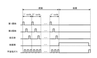
- FIG. 4 is a diagram showing a processing sequence in the first aspect of the present disclosure.
- FIG. 5 is a diagram showing a processing sequence in the second aspect of the present disclosure.
- the processing furnace 202 of the processing apparatus has a heater 207 as a temperature adjustment unit (heating unit).
- the heater 207 is cylindrical and is installed vertically by being supported by a holding plate.
- the heater 207 also functions as an activation mechanism (excitation unit) that activates (excites) the gas by heat.
- a reaction tube 203 is disposed concentrically with the heater 207 inside the heater 207.
- the reaction tube 203 is made of a heat-resistant material such as quartz (SiO 2 ) or silicon carbide (SiC) and is formed in a cylindrical shape with a closed upper end and an open lower end.
- a manifold 209 is disposed concentrically with the reaction tube 203 below the reaction tube 203.
- the manifold 209 is made of a metal material such as stainless steel (SUS) and is formed in a cylindrical shape with an open upper end and a closed lower end. The upper end of the manifold 209 is engaged with the lower end of the reaction tube 203 and is configured to support the reaction tube 203.
- An O-ring 220a is provided between the manifold 209 and the reaction tube 203 as a seal member.
- the reaction tube 203 is installed vertically like the heater 207.
- the reaction tube 203 and the manifold 209 mainly constitute a processing vessel (reaction vessel).
- a processing chamber 201 is formed in a cylindrical hollow portion of the processing vessel.
- the processing chamber 201 is configured to be capable of accommodating a wafer 200 as a substrate. In the processing chamber 201, processing of the wafer 200 is performed.
- Nozzles 249a to 249c serving as first to third supply units are provided within the processing chamber 201, penetrating the sidewall of the manifold 209, respectively. Nozzles 249a to 249c are also referred to as first to third nozzles, respectively. Nozzles 249a to 249c are made of a heat-resistant material such as quartz or SiC. Gas supply pipes 232a to 232c are connected to nozzles 249a to 249c, respectively. Nozzles 249a to 249c are different nozzles, and each of nozzles 249a, 249c is provided adjacent to nozzle 249b.
- Gas supply pipes 232a to 232c are provided with mass flow controllers (MFCs) 241a to 241c, which are flow rate control devices (flow rate control parts), and valves 243a to 243c, which are on-off valves, in order from the upstream side of the gas flow.
- MFCs mass flow controllers
- Gas supply pipes 232d and 232f are connected downstream of valve 243a of gas supply pipe 232a.
- Gas supply pipe 232g is connected downstream of valve 243b of gas supply pipe 232b.
- Gas supply pipes 232e and 232h are connected downstream of valve 243c of gas supply pipe 232c.
- Gas supply pipes 232d to 232h are provided with MFCs 241d to 241h and valves 243d to 243h, in order from the upstream side of the gas flow.
- Gas supply pipes 232a to 232h are made of a metal material, such as SUS.
- the nozzles 249a to 249c are provided in a circular space between the inner wall of the reaction tube 203 and the wafer 200 in a plan view, from the lower part to the upper part of the inner wall of the reaction tube 203, so as to rise upward in the arrangement direction of the wafer 200. That is, the nozzles 249a to 249c are provided in a region horizontally surrounding the wafer arrangement region on the side of the wafer arrangement region in which the wafers 200 are arranged, so as to extend along the wafer arrangement region. In a plan view, the nozzle 249b is arranged to face the exhaust port 231a (described later) in a straight line across the center of the wafer 200 in the processing chamber 201.
- the nozzles 249a and 249c are arranged to sandwich a straight line L passing through the nozzle 249b and the center of the exhaust port 231a from both sides along the inner wall of the reaction tube 203 (the outer periphery of the wafer 200).
- the straight line L is also a straight line passing through the nozzle 249b and the center of the wafer 200.
- nozzle 249c is provided on the opposite side of nozzle 249a across line L.
- Nozzles 249a and 249c are arranged symmetrically with line L as the axis of symmetry.
- Gas supply holes 250a to 250c for supplying gas are provided on the side surfaces of nozzles 249a to 249c, respectively. Each of gas supply holes 250a to 250c opens so as to face exhaust port 231a in plan view, making it possible to supply gas toward wafer 200.
- a plurality of gas supply holes 250a to 250c are provided from the bottom to the top of reaction tube 203.
- raw materials having substructures X and Y are supplied into the processing chamber 201 via the MFC 241a, the valve 243a, and the nozzle 249a.
- the second raw material having partial structure Y is supplied from gas supply pipe 232b into processing chamber 201 via MFC 241b, valve 243b, and nozzle 249b.
- the reactant is supplied from the gas supply pipe 232c into the processing chamber 201 via the MFC 241c, the valve 243c, and the nozzle 249c.
- the first raw material having partial structure X is supplied from gas supply pipe 232d into processing chamber 201 via MFC 241d, valve 243d, gas supply pipe 232a, and nozzle 249a.
- the modifier is supplied from the gas supply pipe 232e into the processing chamber 201 via the MFC 241e, the valve 243e, the gas supply pipe 32c, and the nozzle 249c.
- Inert gas is supplied from gas supply pipes 232f-232h into the processing chamber 201 via MFCs 241f-241h, valves 243f-243h, gas supply pipes 232a-232c, and nozzles 249a-249c.
- the inert gas acts as a purge gas, carrier gas, dilution gas, etc.
- the raw material supply system is mainly composed of gas supply pipe 232a, MFC 241a, and valve 243a.
- the first raw material supply system is mainly composed of gas supply pipe 232d, MFC 241d, and valve 243d.
- the second raw material supply system is mainly composed of gas supply pipe 232b, MFC 241b, and valve 243b.
- the raw material supply system, first raw material supply system, and second raw material supply system may each or all be referred to as the raw material supply system.
- the reactant supply system is mainly composed of gas supply pipe 232c, MFC 241c, and valve 243c.
- the modifier exposure system (modifier supply system) is mainly composed of gas supply pipe 232e, MFC 241e, and valve 243e.
- the inert gas supply system is mainly composed of gas supply pipes 232f-232h, MFCs 241f-241h, and valves 243f-243h.
- any or all of the various supply systems described above may be configured as an integrated supply system 248 in which the valves 243a to 243h and the MFCs 241a to 241h are integrated.
- the integrated supply system 248 is connected to each of the gas supply pipes 232a to 232h, and the supply operation of various substances (various gases) into the gas supply pipes 232a to 232h, i.e., the opening and closing operation of the valves 243a to 243h and the flow rate adjustment operation by the MFCs 241a to 241h, are controlled by a controller 121, which will be described later.
- the integrated supply system 248 is configured as an integrated or separate integrated unit, and can be attached and detached from the gas supply pipes 232a to 232h, etc., in units of integrated units, and is configured so that maintenance, replacement, expansion, etc. of the integrated supply system 248 can be performed in units of integrated units.
- An exhaust port 231a for exhausting the atmosphere in the processing chamber 201 is provided at the bottom of the side wall of the reaction tube 203. As shown in FIG. 2, the exhaust port 231a is provided at a position facing the nozzles 249a to 249c (gas supply holes 250a to 250c) across the wafer 200 in a plan view. The exhaust port 231a may be provided along the side wall of the reaction tube 203 from the bottom to the top, that is, along the wafer arrangement area. An exhaust pipe 231 is connected to the exhaust port 231a.
- a vacuum pump 246 as a vacuum exhaust device is connected to the exhaust pipe 231 via a pressure sensor 245 as a pressure detector (pressure detection unit) that detects the pressure in the processing chamber 201 and an APC (Auto Pressure Controller) valve 244 as a pressure regulator (pressure adjustment unit).
- the APC valve 244 is configured to be able to evacuate and stop the evacuation of the processing chamber 201 by opening and closing the valve while the vacuum pump 246 is operating, and further, to be able to adjust the pressure inside the processing chamber 201 by adjusting the valve opening based on pressure information detected by the pressure sensor 245 while the vacuum pump 246 is operating.
- An exhaust system is mainly configured by the exhaust pipe 231, the APC valve 244, and the pressure sensor 245.
- the vacuum pump 246 may be included in the exhaust system.
- a seal cap 219 is provided as a furnace port cover body capable of airtightly closing the lower end opening of the manifold 209.
- the seal cap 219 is made of a metal material such as SUS and is formed in a disk shape.
- An O-ring 220b is provided on the upper surface of the seal cap 219 as a sealing member that abuts against the lower end of the manifold 209.
- a rotation mechanism 267 is installed to rotate the boat 217 described later.
- the rotation shaft 255 of the rotation mechanism 267 is connected to the boat 217 through the seal cap 219.
- the rotation mechanism 267 is configured to rotate the wafers 200 by rotating the boat 217.
- the seal cap 219 is configured to be raised and lowered vertically by a boat elevator 115 as a lifting mechanism installed outside the reaction tube 203.
- the boat elevator 115 is configured as a transport device (transport mechanism) that transports the wafers 200 in and out of the processing chamber 201 by raising and lowering the seal cap 219.
- a shutter 219s is provided as a furnace port cover that can airtightly close the lower end opening of the manifold 209 when the seal cap 219 is lowered and the boat 217 is removed from the processing chamber 201.
- the shutter 219s is made of a metal material such as SUS and is formed in a disk shape.
- An O-ring 220c is provided on the upper surface of the shutter 219s as a sealing member that abuts against the lower end of the manifold 209.
- the opening and closing operation of the shutter 219s (lifting and lowering operation, rotating operation, etc.) is controlled by a shutter opening and closing mechanism 115s.
- the boat 217 as a substrate support is configured to support multiple wafers 200, for example 25 to 200, in a horizontal position and aligned vertically with their centers aligned, i.e., arranged at intervals, in multiple stages.
- the boat 217 is made of a heat-resistant material such as quartz or SiC.
- insulating plates 218 made of a heat-resistant material such as quartz or SiC are supported in multiple stages.
- a temperature sensor 263 is installed inside the reaction tube 203 as a temperature detector. By adjusting the power supply to the heater 207 based on the temperature information detected by the temperature sensor 263, the temperature inside the processing chamber 201 is distributed as desired.
- the temperature sensor 263 is installed along the inner wall of the reaction tube 203.
- the controller 121 which is a control unit (control means), is configured as a computer equipped with a CPU (Central Processing Unit) 121a, a RAM (Random Access Memory) 121b, a storage device 121c, and an I/O port 121d.
- the RAM 121b, the storage device 121c, and the I/O port 121d are configured to be able to exchange data with the CPU 121a via an internal bus 121e.
- An input/output device 122 configured as, for example, a touch panel is connected to the controller 121.
- an external storage device 123 can be connected to the controller 121.
- the processing device may be configured to have one control unit or multiple control units.
- control for performing the processing sequence described below may be performed using one control unit or multiple control units.
- the multiple control units may be configured as a control system connected to each other via a wired or wireless communication network, and the control for carrying out the processing sequence described below may be performed by the entire control system.
- control unit may include one control unit, multiple control units, or a control system configured by multiple control units.
- the storage device 121c is composed of, for example, a flash memory, a HDD (Hard Disk Drive), an SSD (Solid State Drive), etc.
- a control program for controlling the operation of the processing device, a process recipe describing the procedures and conditions of the substrate processing described later, etc. are recorded and stored in a readable manner.
- the process recipe is a combination of the procedures in the substrate processing described later, which are executed by the controller 121 in the processing device, so that a predetermined result can be obtained, and functions as a program.
- the process recipe, the control program, etc. are collectively referred to simply as a program.
- the process recipe is also simply referred to as a recipe.
- the word program is used in this specification, it may include only a recipe, only a control program, or both.
- the RAM 121b is configured as a memory area (work area) in which the programs and data read by the CPU 121a are temporarily stored.
- the I/O port 121d is connected to the above-mentioned MFCs 241a to 241h, valves 243a to 243h, pressure sensor 245, APC valve 244, vacuum pump 246, temperature sensor 263, heater 207, rotation mechanism 267, boat elevator 115, shutter opening/closing mechanism 115s, etc.
- the CPU 121a is configured to read and execute a control program from the storage device 121c, and to read a recipe from the storage device 121c in response to input of an operation command from the input/output device 122, etc.
- the CPU 121a is configured to control the flow rate adjustment of various substances (various gases) by the MFCs 241a to 241h, the opening and closing of the valves 243a to 243h, the opening and closing of the APC valve 244 and the pressure adjustment by the APC valve 244 based on the pressure sensor 245, the start and stop of the vacuum pump 246, the temperature adjustment of the heater 207 based on the temperature sensor 263, the rotation and rotation speed adjustment of the boat 217 by the rotation mechanism 267, the raising and lowering of the boat 217 by the boat elevator 115, the opening and closing of the shutter 219s by the shutter opening and closing mechanism 115s, etc.
- the controller 121 can be configured by installing the above-mentioned program recorded and stored in the external storage device 123 into a computer.
- the external storage device 123 includes, for example, a magnetic disk such as an HDD, an optical disk such as a CD, a magneto-optical disk such as an MO, and a semiconductor memory such as a USB memory or an SSD.
- the storage device 121c and the external storage device 123 are configured as computer-readable recording media. Hereinafter, these are collectively referred to as recording media.
- recording medium When the term recording medium is used in this specification, it may include only the storage device 121c alone, only the external storage device 123 alone, or both.
- the program may be provided to the computer using a communication means such as the Internet or a dedicated line, without using the external storage device 123.
- processing apparatus is also referred to as a substrate processing apparatus, a film forming processing apparatus, or a film forming apparatus.
- the processing method is also referred to as a substrate processing method, a film forming processing method, or a film forming method.
- a cycle including a step of supplying a raw material having substructures X and Y to wafer 200 (raw material supply step) and a step of supplying a reactant to wafer 200 (reactant supply step) is performed a predetermined number of times (n times, n is an integer of 1 or 2 or more) in the film formation step.
- wafer used in this specification can mean the wafer itself, or a laminate of the wafer and a specified layer or film formed on its surface.
- surface of a wafer used in this specification can mean the surface of the wafer itself, or the surface of a specified layer, etc. formed on the wafer.
- raw material include at least one of gaseous and liquid substances.
- Liquid substances include mist substances.
- each of the raw material, reactant, and modifier may contain a gaseous substance, a liquid substance such as a mist substance, or both.
- the term "layer” includes at least one of a continuous layer and a discontinuous layer.
- the first layer and the second layer may each include a continuous layer, a discontinuous layer, or both.
- the inside of the processing chamber 201 i.e., the space in which the wafer 200 is present, is evacuated (reduced pressure exhaust) by the vacuum pump 246 so that the inside of the processing chamber 201 is at a desired pressure (vacuum level).
- the pressure inside the processing chamber 201 is measured by the pressure sensor 245, and the APC valve 244 is feedback-controlled based on the measured pressure information.
- the wafer 200 inside the processing chamber 201 is heated by the heater 207 so that the wafer 200 is at a desired processing temperature.
- the power supply to the heater 207 is feedback-controlled based on the temperature information detected by the temperature sensor 263 so that the inside of the processing chamber 201 has a desired temperature distribution.
- the rotation mechanism 267 starts rotating the wafer 200. The evacuation inside the processing chamber 201 and the heating and rotation of the wafer 200 are all continued at least until the processing of the wafer 200 is completed.
- a raw material (raw material gas) is supplied to the wafer 200 .
- valve 243a is opened to allow the raw material to flow into gas supply pipe 232a.
- the raw material has its flow rate adjusted by MFC 241a, is supplied into processing chamber 201 via nozzle 249a, and is exhausted from exhaust port 231a.
- the raw material is supplied to wafer 200 from the side of wafer 200 (raw material supply).
- valves 243f to 243h may be opened to supply an inert gas into processing chamber 201 via nozzles 249a to 249c, respectively.
- the processing conditions when supplying the raw material in the raw material supply step are as follows: Treatment temperature: room temperature to 700°C, preferably 60 to 600°C Treatment pressure: 1 to 2666 Pa, preferably 10 to 1333 Pa Raw material supply flow rate: 10 to 10,000 sccm, preferably 100 to 2,000 sccm Raw material supply time: 1 to 240 seconds, preferably 5 to 120 seconds Inert gas supply flow rate (per gas supply pipe): 0 to 20,000 sccm Examples include:
- the process temperature means the temperature of the wafer 200 or the temperature inside the process chamber 201
- the process pressure means the pressure inside the process chamber 201.
- the process time means the time that the process continues.
- the supply flow rate includes 0 sccm
- 0 sccm means that the substance (gas) is not supplied.
- a substance (gas) having partial structure X and partial structure Y can be used as a raw material.
- the partial structure X includes, for example, at least one of Si-CH 2 -Si, Si-CH 2 -CH 2 -Si, Si-R, N(SiR ' 3 ) 3 and CSi 3 H.
- the partial structure Y includes, for example, at least one of Si-OR', Si-NR'-Si, Si-NR' 2 , NR' 3 , Si-Cl, Si-Br, Si-I, B-Cl, B-Br, B-I and Si-H.
- Si stands for silicon
- C stands for carbon
- H stands for hydrogen
- N stands for nitrogen
- O stands for oxygen
- B stands for boron
- Cl stands for chlorine
- Br stands for bromine
- I stands for iodine.
- R represents an alkyl group, and each of the R' groups independently represents a hydrogen atom or an alkyl group.
- the alkyl group is preferably an alkyl group having 1 to 5 carbon atoms, and more preferably an alkyl group having 1 to 4 carbon atoms.
- the alkyl group may be linear or branched. Examples of the alkyl group include a methyl group, an ethyl group, an n-propyl group, an n-butyl group, an isopropyl group, an isobutyl group, a sec-butyl group, and a tert-butyl group.
- OR' represents an alkoxy group.
- the alkoxy group is preferably an alkoxy group having 1 to 5 carbon atoms, and more preferably an alkoxy group having 1 to 4 carbon atoms.
- the alkyl group in the alkoxy group represented by OR' is the same as the alkyl group described above.
- NR'2 represents an amino group.
- the amino group is preferably an amino group having 1 to 5 carbon atoms, and more preferably an amino group having 1 to 4 carbon atoms.
- the alkyl group in the amino group represented by NR'2 is the same as the alkyl group described above.
- the multiple R's may be the same or different.
- a Si-containing substance such as H 3 Si—CH 2 —CH 2 —SiH 2 OR′ gas, N(SiH 3 ) 2 (SiH 2 OR′) gas, N(SiH 3 ) 2 SiH 2 NR′ 2 gas, etc.
- a Si-containing substance such as H 3 Si—CH 2 —CH 2 —SiH 2 OR′ gas, N(SiH 3 ) 2 (SiH 2 OR′) gas, N(SiH 3 ) 2 SiH 2 NR′ 2 gas, etc.
- a Si-containing substance such as H 3 Si—CH 2 —CH 2 —SiH 2 OR′ gas, N(SiH 3 ) 2 (SiH 2 OR′) gas, N(SiH 3 ) 2 SiH 2 NR′ 2 gas, etc.
- one or more of these can be used.
- N2 gas or a rare gas such as argon (Ar) gas, helium (He) gas, neon (Ne) gas, or xenon (Xe) gas can be used.
- Ar argon
- He helium
- Ne neon
- Xe xenon
- the inert gas one or more of these can be used. This also applies to each step described later.
- valve 243a is closed to stop the supply of raw materials into the processing chamber 201. Then, the processing chamber 201 is evacuated to remove gaseous substances remaining in the processing chamber 201 from the processing chamber 201. At this time, valves 243f to 243h are opened to supply an inert gas into the processing chamber 201 through nozzles 249a to 249c. The inert gas supplied from nozzles 249a to 249c acts as a purge gas, thereby purging the processing chamber 201 (purge). It is preferable that the processing temperature when purging in this step is the same as the processing temperature when the raw materials are supplied.
- reactant Supply Step After the raw material supply step is completed, a reactant (reaction gas) is supplied to the wafer 200, that is, the wafer 200 after the first layer is formed on the surface thereof.
- valve 243c is opened to allow reactants to flow into gas supply pipe 232c.
- the reactants are adjusted in flow rate by MFC 241c, supplied into processing chamber 201 via nozzle 249c, and exhausted from exhaust port 231a.
- reactants are supplied to wafer 200 from the side of wafer 200 (reactant supply).
- valves 243f to 243h may be opened to supply an inert gas into processing chamber 201 via nozzles 249a to 249c, respectively.
- the process conditions for supplying the reactants in the reactant supply step are as follows: Treatment pressure: 1 to 13332 Pa, preferably 10 to 1333 Pa Reactant supply flow rate: 10-10000 sccm, preferably 100-2000 sccm Reactant supply time: 1 to 240 seconds, preferably 5 to 120 seconds Other processing conditions may be the same as those in the raw material supply step.
- the reactant may be, for example, an oxygen (O)-containing substance (gas).
- O-containing substance examples include O2 gas, O3 gas, N2O gas, NO2 gas, NO gas, CO2 gas, and CO gas.
- the reactant may be, for example, a nitrogen (N) and hydrogen (H)-containing substance (gas).
- N and H-containing substance include NH3 gas, N2H2 gas , N2H4 gas , and N3H8 gas.
- One or more of these can be used as reactants.
- the valve 243c is closed to stop the supply of reactants into the processing chamber 201. Then, gaseous substances remaining in the processing chamber 201 are removed from the processing chamber 201 (purging) using the same processing procedure and processing conditions as the purging in the raw material supply step. It is preferable that the processing temperature when purging in this step is the same as the processing temperature when supplying the reactants.
- the above-mentioned raw material supply step and reactant supply step are performed asynchronously, i.e., by performing a cycle of n times (n is an integer of 1 or 2 or more) in this order, it is possible to form a first film on the surface of the wafer 200. It is preferable to repeat the above-mentioned cycle multiple times. That is, it is preferable to make the thickness of the second layer formed per cycle thinner than the desired film thickness, and to repeat the above-mentioned cycle multiple times until the film thickness of the first film formed by stacking the second layers reaches the desired film thickness.
- Si-containing material When the above-mentioned Si-containing material is used as a raw material and the above-mentioned O-containing material is used as a reactant, a film containing Si and O, i.e., a silicon oxide film (SiO film), is formed on the surface of the wafer 200.
- SiO film silicon oxide film
- N- and H-containing material When the above-mentioned Si-containing material is used as a raw material and the above-mentioned N- and H-containing material is used as a reactant, a film containing Si and N, i.e., a silicon nitride film (SiN film), is formed on the surface of the wafer 200.
- SiN film silicon nitride film
- the first film will be a film containing at least a portion of partial structure X and partial structure Z derived from partial structure Y.
- the partial structure X includes at least one of, for example, Si-CH 2 -Si, Si-CH 2 -CH 2 -Si, Si-R, N(SiR ' 3 ) 3 and CSi 3 H.
- the first film may include Si-CH 2 -Si itself as at least a part of the partial structure X, or may include a structure in which a specific atom has been removed from the partial structure X, such as Si-CH 2.
- the first film may include Si-CH 2 -CH 2 -Si itself as at least a part of the partial structure X, or may include a structure in which a specific atom has been removed from the partial structure X, such as Si-CH 2 -CH 2 or Si-CH 2 .
- Substructure Z is a structure derived from substructure Y.
- Substructure Z can be said to be a structure generated in the process of a raw material having substructure Y chemically reacting with the surface of the wafer 200, or in other words, a structure generated in the process of a raw material having substructure Y being thermally decomposed.
- Substructure Z may have the same chemical structure as substructure Y. That is, substructure Z may be obtained by incorporating substructure Y directly into the first film.
- Substructure Z may also be generated by altering substructure Y. That is, substructure Z may be generated by changing at least one of the composition and chemical structure of substructure Y. For these reasons, substructure Y can be said to be a structure that is the source of generating substructure Z in the first film.
- the partial structure Y includes at least one of, for example, Si-OR', Si-NR'-Si, Si-NR' 2 , NR' 3 , Si-Cl, Si-Br, Si-I, B-Cl, B-Br, B-I, and Si-H. Therefore, the partial structure Z derived from the partial structure Y includes at least one of, for example, Si-OR', Si-NR'-Si, Si-NR' 2 , Si-Cl, Si-Br, Si-I, B-Cl, B-Br, B-I, and Si-H.
- the first film may include Si-NR'-Si itself as the partial structure Z derived from the partial structure Y, or may include a structure in which Si and R' are replaced, such as Si-NR' 2 .
- the first film may contain Si— NR′2 itself as the partial structure Z derived from the partial structure Y, or may contain a structure in which R′ is replaced by Si, such as Si—NR′-Si.
- Modification step Thereafter, a subsequent modifier exposure step is performed.
- the film formed on the surface of the wafer 200 that is, the first film including at least a part of the substructure X and the substructure Z derived from the substructure Y, is exposed to a modifying agent.
- valve 243e is opened to allow the modifying agent to flow into gas supply pipe 232e.
- the flow rate of the modifying agent is adjusted by MFC 241e, and the modifying agent is supplied into processing chamber 201 via gas supply pipe 232c and nozzle 249c, and exhausted from exhaust port 231a.
- the modifying agent is supplied to wafer 200 from the side of wafer 200, and the first film formed on the surface of wafer 200 is exposed to the modifying agent, causing the first film to react with the modifying agent (modifying agent exposure).
- valves 243f to 243h may be opened to supply an inert gas into processing chamber 201 via nozzles 249a to 249c, respectively.
- This step is preferably carried out under conditions in which the reactivity of the partial structure Z contained in the first film with the modifier is higher than the reactivity of at least a portion of the partial structure X contained in the first film with the modifier.
- this step is preferably performed under conditions that allow at least a portion of the substructure X contained in the first film to be maintained.
- this step is preferably performed under conditions that make it possible to change at least one of the composition and chemical structure of at least a part of the partial structure Z contained in the first film.
- this step is preferably performed under conditions that make it possible to change at least a part of the partial structure Z contained in the first film to a different partial structure V.
- the number of elements constituting the partial structure V may be less than the number of elements constituting the partial structure Z.
- this step is preferably performed under conditions that make it possible to remove at least one of the elements constituting the partial structure Z contained in the first film and/or replace it with another element.
- the case of removing at least one of the elements constituting the partial structure Z contained in the first film includes the case of removing one element, the case of removing multiple elements, and the case of removing all elements, among the elements constituting the partial structure Z.
- the partial structure Z is Si-OR'
- this case includes the case of removing Si, removing R', and removing Si-OR' itself, among the elements constituting the partial structure Z.
- the partial structure Z is Si-NR'-Si
- this case includes the case of removing Si, removing R', and removing Si-NR'-Si itself, among the elements constituting the partial structure Z.
- cases other than the case of removing the partial structure Z itself are examples of changing the composition of at least a part of the partial structure Z, and are also examples of changing the chemical structure of at least a part of the partial structure Z.
- cases other than the case of removing the partial structure Z itself are examples of changing at least a part of the partial structure Z to a different partial structure V, and are also examples in which the number of elements constituting the partial structure V is less than the number of elements constituting the partial structure Z.
- the structure remaining after removing at least one of the elements that make up substructure Z is substructure V.
- the case where at least one of the elements constituting the partial structure Z contained in the first film is replaced with another element includes the case where one element of the elements constituting the partial structure Z is replaced with another element, the case where multiple elements are replaced with other elements, and the case where all elements are replaced with other elements.
- the partial structure Z is Si-OR'
- this case includes the case where, among the elements constituting the partial structure Z, Si is replaced with R', R' is replaced with Si, and Si-OR' itself is replaced with another element.
- the partial structure Z is Si-NR'-Si
- this case includes the case where, among the elements constituting the partial structure Z, Si is replaced with R', R' is replaced with Si, and Si-NR'-Si itself is replaced with another element.
- the processing conditions for supplying the modifier in the modifier exposure step are as follows: Treatment pressure: 1 to 100,000 Pa, preferably 100 to 100,000 Pa Modifier supply flow rate: 10 to 10,000 sccm, preferably 100 to 2,000 sccm Modifier supply time: 1 to 300 minutes, preferably 10 to 240 minutes. Other processing conditions may be the same as those used when supplying the raw material in the raw material supply step.
- H and O 2 gas for example, a hydrogen (H) and oxygen (O) containing substance (gas) can be used.
- H and O containing substance for example, H 2 O gas, H 2 O 2 gas, H 2 gas + O 2 gas, D 2 gas + O 2 gas, H 2 gas + O 3 gas, D 2 gas + O 3 gas, etc.
- D represents deuterium.
- H 2 gas + O 2 gas means a mixed gas of H 2 gas and O 2 gas.
- the two gases When supplying a mixed gas, the two gases may be mixed (premixed) in a supply pipe and then supplied into the processing chamber 201, or the two gases may be supplied separately from different supply pipes into the processing chamber 201 and mixed (postmixed) in the processing chamber 201.
- the modifier one or more of these can be used.
- the first film formed on the surface of the wafer 200 is exposed to the above-mentioned modifier under the above-mentioned processing conditions, thereby making it possible to react the first film with the reactant.
- This makes it possible to modify (change) the first film into a second film that contains at least a part of the partial structure X and has a smaller amount of the partial structure Z than the amount of the partial structure Z contained in the first film.
- This makes it possible to change the first film into a second film having a density lower than that of the first film.
- this step it may be possible to change at least a part of the partial structure Z contained in the first film into a partial structure containing Si-O-Si, i.e., a partial structure containing siloxane, which makes it possible to further reduce the density of the first film.
- the second film becomes a film containing siloxane bonds.
- the valve 243e is closed to stop the supply of the modifier into the processing chamber 201. Then, gaseous substances remaining in the processing chamber 201 are removed from the processing chamber 201 using the same processing procedures and conditions as the purging in the raw material supply step (purging).
- the processing temperature when purging in this step is preferably the same as the processing temperature in the modifier exposure step.
- an inert gas is supplied as a purge gas from each of the nozzles 249a to 249c into the processing chamber 201, and exhausted from the exhaust port 231a. This purges the processing chamber 201, and gases and reaction by-products remaining in the processing chamber 201 are removed from the processing chamber 201 (after-purge). Thereafter, the atmosphere in the processing chamber 201 is replaced with the inert gas (inert gas replacement), and the pressure in the processing chamber 201 is returned to normal pressure (atmospheric pressure return).
- the seal cap 219 is lowered by the boat elevator 115, and the lower end of the manifold 209 is opened. Then, the processed wafers 200 are carried out from the lower end of the manifold 209 to the outside of the reaction tube 203 while being supported by the boat 217 (boat unloading). After the boat unloading, the shutter 219s is moved, and the lower end opening of the manifold 209 is sealed by the shutter 219s via the O-ring 220c (shutter close). After being carried out to the outside of the reaction tube 203, the processed wafers 200 are taken out of the boat 217 (wafer discharge).
- the amount of partial structure Z contained in the second film can be effectively reduced compared to the amount of partial structure Z contained in the first film, and the density of the second film can be effectively reduced and the k value of the second film can be effectively reduced. That is, the low-k nature of the second film can be effectively realized.
- the number of elements constituting the partial structure V may be less than the number of elements constituting the partial structure Z, which makes it possible to more effectively reduce the density of the second film and the k value of the second film. That is, the low-k nature of the second film can be effectively realized.
- the partial structure X includes at least one of Si-CH 2 -Si, Si-CH 2 -CH 2 -Si, Si-R, N(SiR ' 3 ) 3 and CSi 3 H
- the partial structure Y includes at least one of Si-OR', Si-NR'-Si, Si-NR' 2 , NR' 3 , Si-Cl, Si-Br, Si-I, B-Cl, B-Br, B-I and Si-H
- the partial structure Z includes at least one of Si-OR', Si-NR'-Si, Si-NR' 2 , Si-Cl, Si-Br, Si-I, B-Cl, B-Br, B-I and Si-H, thereby making it possible to effectively cause the above-mentioned reaction.
- partial structure Z has the same chemical structure as partial structure Y, i.e., partial structure Z is obtained by incorporating partial structure Y into the first film, it is possible to effectively cause the above-mentioned reaction.
- the partial structure Z is generated by altering the partial structure Y, i.e., the partial structure Z is generated by changing at least one of the composition and chemical structure of the partial structure Y, thereby making it possible to effectively cause the above-mentioned reaction.
- the processing sequence in this embodiment differs from the first embodiment described above in that a first source material having a partial structure X and a second source material having a partial structure Y are supplied in the film formation step. Other points are the same as those in the first embodiment.
- a cycle including a step of supplying a first source having a substructure X to the wafer 200 (first source supply step), a step of supplying a second source having a substructure Y to the wafer 200 (second source supply step), and a step of supplying a reactant to the wafer 200 (reactant supply step) is performed a predetermined number of times (n times, n is an integer of 1 or 2 or more) in the film formation step.
- valve 243d is opened and the first raw material is flowed into gas supply pipe 232d.
- the flow rate of the first raw material is adjusted by MFC 241d, and the first raw material is supplied into processing chamber 201 via gas supply pipe 232a and nozzle 249a, and exhausted from exhaust port 231a.
- the first raw material is supplied to wafer 200 from the side of wafer 200 (first raw material supply).
- valves 243f to 243h may be opened to supply an inert gas into processing chamber 201 via each of nozzles 249a to 249c.
- the processing conditions for supplying the first raw material in the first raw material supplying step are as follows: First raw material supply flow rate: 10 to 10,000 sccm, preferably 100 to 2,000 sccm First raw material supply time: 1 to 240 seconds, preferably 5 to 120 seconds. Other processing conditions can be the same as the processing conditions when the raw material is supplied in the raw material supply step of the first embodiment.
- a substance (gas) having at least one of the partial structures X exemplified in the first embodiment for example, Si-CH 2 -Si, Si-CH 2 -CH 2 -Si, Si-R, N(SiR' 3 ) 3 , and CSi 3 H, can be used.
- the first raw material for example, SiH 3 CH 2 SiH 3 gas, SiH 3 CH 2 CH 2 SiH 3 gas, SiH 2 (CH 3 ) 2 gas, and N(SiH 3 ) 3 gas can be used.
- SiH 3 CH 2 SiH 3 gas SiH 3 CH 2 CH 2 SiH 3 gas
- SiH 2 (CH 3 ) 2 gas, and N(SiH 3 ) 3 gas can be used.
- one or more of these can be used.
- valve 243d is closed to stop the supply of the first raw material into processing chamber 201. Then, gaseous substances remaining in processing chamber 201 are removed from processing chamber 201 (purging) using the same processing procedures and conditions as the purging in the raw material supply step of the first embodiment. It is preferable that the processing temperature when purging in this step is the same as the processing temperature when supplying the first raw material.
- valve 243b is opened to allow the second raw material to flow into gas supply pipe 232b.
- the flow rate of the second raw material is adjusted by MFC 241b, and the second raw material is supplied into processing chamber 201 via nozzle 249b and exhausted from exhaust port 231a.
- the second raw material is supplied to wafer 200 from the side of wafer 200 (second raw material supply).
- valves 243f to 243h may be opened to supply an inert gas into processing chamber 201 via nozzles 249a to 249c, respectively.
- the processing conditions for supplying the second raw material in the second raw material supplying step are as follows: Second raw material supply flow rate: 10 to 10,000 sccm, preferably 100 to 2,000 sccm Second raw material supply time: 1 to 240 seconds, preferably 5 to 120 seconds. Other processing conditions can be the same as the processing conditions when the raw material is supplied in the raw material supply step of the first embodiment.
- a substance (gas) having at least one of the partial structure Y exemplified in the first embodiment for example, Si-OR', Si-NR'-Si, Si- NR'2 , NR'3 , Si-Cl, Si-Br, Si-I, B-Cl, B-Br, B-I, and Si-H
- Si-OR' Si-NR'-Si, Si- NR'2 , NR'3 , Si-Cl, Si-Br, Si-I, B-Cl, B-Br, B-I, and Si-H
- Si-OR' for example, H3Si - CH2 - CH2 -SiH2OR' gas, ( CH3 ) 3SiNHSi ( CH3 ) 3 gas, N ( SiH3 ) 2SiH2NR'2 gas, NH3 gas, and Si3Cl8 gas can be used.
- one or more of these can be used.
- valve 243b is closed to stop the supply of the second raw material into processing chamber 201. Then, gaseous substances remaining in processing chamber 201 are removed from processing chamber 201 (purging) using the same processing procedures and conditions as the purging in the raw material supply step of the first embodiment. It is preferable that the processing temperature when purging in this step is the same as the processing temperature when the second raw material is supplied.
- the process procedure and process conditions in the reactant supply step of the second embodiment can be the same as those in the reactant supply step of the first embodiment.
- Substructure Z derived from substructure Y includes at least one of, for example, Si-OR', Si-NR'-Si, Si-NR' 2 , Si-Cl, Si-Br, Si-I, B-Cl, B-Br, B-I, and Si-H, similar to the first embodiment.
- a modification step is performed, in which the first film formed on the surface of the wafer 200 is exposed to a modifier and reacted with the modifier.
- the processing procedure and processing conditions in the modification step of the second aspect can be the same as those in the modification step of the first aspect.
- the first film it is also possible to modify (change) the first film into a second film that contains at least a part of the partial structure X and has a smaller amount of the partial structure Z than the amount of the partial structure Z contained in the first film.
- This makes it possible to change the first film into a second film having a density lower than that of the first film.
- the second film becomes a porous film.
- the second film becomes a film containing siloxane bonds.
- the same effect as in the first embodiment can be obtained.
- the substrate may be processed according to the processing sequence shown below (n is an integer of 1 or 2 or more).
- n is an integer of 1 or 2 or more.
- the substrate may be processed according to the processing sequence shown below (where m and n are integers of 1 or 2 or more). In these embodiments, the same effects as those in the above embodiment can be obtained.
- a step of supplying a catalyst to the substrate may be performed at the timing of starting each cycle of the film formation step, as shown in the processing sequence shown below (n is an integer of 1 or 2 or more).
- a “catalyst” refers to a substance that does not change itself before and after a chemical reaction, but does change the rate of the reaction.
- the catalyst in the reaction system of this embodiment has a catalytic effect that changes the rate of the reaction, but part of the molecular structure may decompose during the reaction process, and the catalyst itself may change before and after the chemical reaction.
- substances that have a catalytic effect that changes the rate of a reaction including those that do not change before and after a chemical reaction, as well as those that may change before and after a chemical reaction, are referred to as catalysts.
- a boron (B)-containing substance gas
- B boron
- BClH2 gas, BCl2H gas, BCl3 gas, BF3 gas, BBr3 gas, and B2H6 gas can be used.
- F represents fluorine.
- the treatment conditions for supplying the catalyst are as follows: Catalyst supply flow rate: 10 to 10,000 sccm, preferably 100 to 2,000 sccm Catalyst supply time: 1 to 240 seconds, preferably 5 to 120 seconds.
- Other treatment conditions may be the same as those used when supplying the raw material in the raw material supply step of the first embodiment.
- the atmosphere may be introduced into the processing chamber, and the modifier exposure step may be performed in the atmosphere.
- the substrate may be removed from the processing chamber, and the modifier exposure step may be performed in the atmosphere.
- oxygen (O 2 ) or moisture (H 2 O) contained in the atmosphere may be used as the modifier. In these cases, the same effects as those of the above-mentioned aspect can be obtained.
- the recipes used for each process are preferably prepared individually according to the process content, and recorded and stored in the storage device 121c via an electric communication line or external storage device 123. Then, when starting each process, the CPU 121a preferably selects an appropriate recipe according to the process content from among the multiple recipes recorded and stored in the storage device 121c. This makes it possible to reproducibly form films of various film types, composition ratios, film qualities, and film thicknesses in the processing device. It also reduces the burden on the operator, and allows each process to be started quickly while avoiding operating errors.
- the above-mentioned recipes do not necessarily have to be created anew, but may be prepared, for example, by modifying an existing recipe that has already been installed in the processing device.
- the modified recipe may be installed in the processing device via a telecommunications line or a recording medium on which the recipe is recorded.
- an existing recipe that has already been installed in the processing device may be directly modified by operating the input/output device 122 provided in the existing processing device.
- an example of forming a film using a batch-type processing apparatus that processes multiple substrates at a time has been described.
- the present disclosure is not limited to the above-mentioned embodiment, and can be suitably applied, for example, to a case where a film is formed using a single-wafer processing apparatus that processes one or several substrates at a time.
- an example of forming a film using a processing apparatus having a hot-wall type processing furnace has been described.
- the present disclosure is not limited to the above-mentioned embodiment, and can be suitably applied to a case where a film is formed using a processing apparatus having a cold-wall type processing furnace.
- each process can be performed using the same processing procedures and conditions as the above-mentioned aspects and modifications, and the same effects as the above-mentioned aspects and modifications can be obtained.
Landscapes
- Chemical & Material Sciences (AREA)
- General Chemical & Material Sciences (AREA)
- Chemical Kinetics & Catalysis (AREA)
- Engineering & Computer Science (AREA)
- Materials Engineering (AREA)
- Mechanical Engineering (AREA)
- Metallurgy (AREA)
- Organic Chemistry (AREA)
- Inorganic Chemistry (AREA)
- Chemical Vapour Deposition (AREA)
Abstract
(a)基板に対して、部分構造Xと部分構造Yとを有する原料を供給することで、もしくは、前記部分構造Xを有する第1原料と前記部分構造Yを有する第2原料とを供給することで、前記基板の表面上に、前記部分構造Xの少なくとも一部と前記部分構造Yに由来する部分構造Zとを含む第1膜を形成する工程と、(b)前記基板上に形成された前記第1膜を改質剤に曝露させることで、前記第1膜を、前記部分構造Xの少なくとも一部を含み前記部分構造Zの量が前記第1膜に含まれる前記部分構造Zの量よりも少ない第2膜に改質させる工程と、を有する。
Description
本開示は、処理方法、半導体装置の製造方法、処理装置、およびプログラムに関する。
半導体装置の製造工程の一工程として、基板上に膜を形成する処理が行われることがある(例えば特許文献1参照)。
本開示は、基板上に形成される膜の加工耐性の向上および低誘電率化を実現することが可能な技術を提供する。
本開示の一態様によれば、
(a)基板に対して、部分構造Xと部分構造Yとを有する原料を供給することで、もしくは、前記部分構造Xを有する第1原料と前記部分構造Yを有する第2原料とを供給することで、前記基板の表面上に、前記部分構造Xの少なくとも一部と前記部分構造Yに由来する部分構造Zとを含む第1膜を形成する工程と、
(b)前記基板上に形成された前記第1膜を改質剤に曝露させることで、前記第1膜を、前記部分構造Xの少なくとも一部を含み前記部分構造Zの量が前記第1膜に含まれる前記部分構造Zの量よりも少ない第2膜に改質させる工程と、
を有する技術が提供される。
(a)基板に対して、部分構造Xと部分構造Yとを有する原料を供給することで、もしくは、前記部分構造Xを有する第1原料と前記部分構造Yを有する第2原料とを供給することで、前記基板の表面上に、前記部分構造Xの少なくとも一部と前記部分構造Yに由来する部分構造Zとを含む第1膜を形成する工程と、
(b)前記基板上に形成された前記第1膜を改質剤に曝露させることで、前記第1膜を、前記部分構造Xの少なくとも一部を含み前記部分構造Zの量が前記第1膜に含まれる前記部分構造Zの量よりも少ない第2膜に改質させる工程と、
を有する技術が提供される。
本開示によれば、基板上に形成される膜の加工耐性の向上および低誘電率化を実現することが可能となる。
<本開示の第1態様>
以下、本開示の第1態様について、主に、図1~図4を参照しつつ説明する。なお、以下の説明において用いられる図面は、いずれも模式的なものであり、図面に示される、各要素の寸法の関係、各要素の比率等は、現実のものとは必ずしも一致していない。また、複数の図面の相互間においても、各要素の寸法の関係、各要素の比率等は必ずしも一致していない。
以下、本開示の第1態様について、主に、図1~図4を参照しつつ説明する。なお、以下の説明において用いられる図面は、いずれも模式的なものであり、図面に示される、各要素の寸法の関係、各要素の比率等は、現実のものとは必ずしも一致していない。また、複数の図面の相互間においても、各要素の寸法の関係、各要素の比率等は必ずしも一致していない。
(1)処理装置の構成
図1に示すように、処理装置の処理炉202は温度調整部(加熱部)としてのヒータ207を有する。ヒータ207は円筒形状であり、保持板に支持されることにより垂直に据え付けられている。ヒータ207は、ガスを熱で活性化(励起)させる活性化機構(励起部)としても機能する。
図1に示すように、処理装置の処理炉202は温度調整部(加熱部)としてのヒータ207を有する。ヒータ207は円筒形状であり、保持板に支持されることにより垂直に据え付けられている。ヒータ207は、ガスを熱で活性化(励起)させる活性化機構(励起部)としても機能する。
ヒータ207の内側には、ヒータ207と同心円状に反応管203が配設されている。反応管203は、例えば石英(SiO2)または炭化シリコン(SiC)等の耐熱性材料により構成され、上端が閉塞し下端が開口した円筒形状に形成されている。反応管203の下方には、反応管203と同心円状にマニホールド209が配設されている。マニホールド209は、例えばステンレス鋼(SUS)等の金属材料により構成され、上端および下端が開口した円筒形状に形成されている。マニホールド209の上端部は、反応管203の下端部に係合しており、反応管203を支持するように構成されている。マニホールド209と反応管203との間には、シール部材としてのOリング220aが設けられている。反応管203はヒータ207と同様に垂直に据え付けられている。主に、反応管203とマニホールド209とにより処理容器(反応容器)が構成される。処理容器の筒中空部には処理室201が形成される。処理室201は、基板としてのウエハ200を収容可能に構成されている。この処理室201内でウエハ200に対する処理が行われる。
処理室201内には、第1~第3供給部としてのノズル249a~249cが、マニホールド209の側壁を貫通するようにそれぞれ設けられている。ノズル249a~249cを、それぞれ第1~第3ノズルとも称する。ノズル249a~249cは、例えば石英またはSiC等の耐熱性材料により構成されている。ノズル249a~249cには、ガス供給管232a~232cがそれぞれ接続されている。ノズル249a~249cはそれぞれ異なるノズルであり、ノズル249a,249cのそれぞれは、ノズル249bに隣接して設けられている。
ガス供給管232a~232cには、ガス流の上流側から順に、流量制御器(流量制御部)であるマスフローコントローラ(MFC)241a~241cおよび開閉弁であるバルブ243a~243cがそれぞれ設けられている。ガス供給管232aのバルブ243aよりも下流側には、ガス供給管232d,232fが接続されている。ガス供給管232bのバルブ243bよりも下流側には、ガス供給管232gが接続されている。ガス供給管232cのバルブ243cよりも下流側には、ガス供給管232e,232hが接続されている。ガス供給管232d~232hには、ガス流の上流側から順に、MFC241d~241hおよびバルブ243d~243hがそれぞれ設けられている。ガス供給管232a~232hは、例えばSUS等の金属材料により構成されている。
図2に示すように、ノズル249a~249cは、反応管203の内壁とウエハ200との間における平面視において円環状の空間に、反応管203の内壁の下部より上部に沿って、ウエハ200の配列方向上方に向かって立ち上がるようにそれぞれ設けられている。すなわち、ノズル249a~249cは、ウエハ200が配列されるウエハ配列領域の側方の、ウエハ配列領域を水平に取り囲む領域に、ウエハ配列領域に沿うようにそれぞれ設けられている。平面視において、ノズル249bは、処理室201内におけるウエハ200の中心を挟んで後述する排気口231aと一直線上に対向するように配置されている。ノズル249a,249cは、ノズル249bと排気口231aの中心とを通る直線Lを、反応管203の内壁(ウエハ200の外周部)に沿って両側から挟み込むように配置されている。直線Lは、ノズル249bとウエハ200の中心とを通る直線でもある。すなわち、ノズル249cは、直線Lを挟んでノズル249aと反対側に設けられているということもできる。ノズル249a,249cは、直線Lを対称軸として線対称に配置されている。ノズル249a~249cの側面には、ガスを供給するガス供給孔250a~250cがそれぞれ設けられている。ガス供給孔250a~250cは、それぞれが、平面視において排気口231aと対向(対面)するように開口しており、ウエハ200に向けてガスを供給することが可能となっている。ガス供給孔250a~250cは、反応管203の下部から上部にわたって複数設けられている。
ガス供給管232aからは、部分構造Xと部分構造Yとを有する原料が、MFC241a、バルブ243a、ノズル249aを介して処理室201内へ供給される。
ガス供給管232bからは、部分構造Yを有する第2原料が、MFC241b、バルブ243b、ノズル249bを介して処理室201内へ供給される。
ガス供給管232cからは、反応体が、MFC241c、バルブ243c、ノズル249cを介して処理室201内へ供給される。
ガス供給管232dからは、部分構造Xを有する第1原料が、MFC241d、バルブ243d、ガス供給管232a、ノズル249aを介して処理室201内へ供給される。
ガス供給管232eからは、改質剤が、MFC241e、バルブ243e、ガス供給管32c、ノズル249cを介して処理室201内へ供給される。
ガス供給管232f~232hからは、不活性ガスが、それぞれMFC241f~241h、バルブ243f~243h、ガス供給管232a~232c、ノズル249a~249cを介して処理室201内へ供給される。不活性ガスは、パージガス、キャリアガス、希釈ガス等として作用する。
主に、ガス供給管232a、MFC241a、バルブ243aにより、原料供給系が構成される。主に、ガス供給管232d、MFC241d、バルブ243dにより、第1原料供給系が構成される。主に、ガス供給管232b、MFC241b、バルブ243bにより、第2原料供給系が構成される。原料供給系、第1原料供給系、第2原料供給系のそれぞれ或いは全てを原料供給系と称する場合もある。主に、ガス供給管232c、MFC241c、バルブ243cにより、反応体供給系が構成される。主に、ガス供給管232e、MFC241e、バルブ243eにより、改質剤曝露系(改質剤供給系)が構成される。主に、ガス供給管232f~232h、MFC241f~241h、バルブ243f~243hにより、不活性ガス供給系が構成される。
上述の各種供給系のうち、いずれか、或いは、全ての供給系は、バルブ243a~243hやMFC241a~241h等が集積されてなる集積型供給システム248として構成されていてもよい。集積型供給システム248は、ガス供給管232a~232hのそれぞれに対して接続され、ガス供給管232a~232h内への各種物質(各種ガス)の供給動作、すなわち、バルブ243a~243hの開閉動作やMFC241a~241hによる流量調整動作等が、後述するコントローラ121によって制御されるように構成されている。集積型供給システム248は、一体型、或いは、分割型の集積ユニットとして構成されており、ガス供給管232a~232h等に対して集積ユニット単位で着脱を行うことができ、集積型供給システム248のメンテナンス、交換、増設等を、集積ユニット単位で行うことが可能なように構成されている。
反応管203の側壁下方には、処理室201内の雰囲気を排気する排気口231aが設けられている。図2に示すように、排気口231aは、平面視において、ウエハ200を挟んでノズル249a~249c(ガス供給孔250a~250c)と対向(対面)する位置に設けられている。排気口231aは、反応管203の側壁の下部より上部に沿って、すなわち、ウエハ配列領域に沿って設けられていてもよい。排気口231aには排気管231が接続されている。排気管231には、処理室201内の圧力を検出する圧力検出器(圧力検出部)としての圧力センサ245および圧力調整器(圧力調整部)としてのAPC(Auto Pressure Controller)バルブ244を介して、真空排気装置としての真空ポンプ246が接続されている。APCバルブ244は、真空ポンプ246を作動させた状態で弁を開閉することで、処理室201内の真空排気および真空排気停止を行うことができ、さらに、真空ポンプ246を作動させた状態で、圧力センサ245により検出された圧力情報に基づいて弁開度を調節することで、処理室201内の圧力を調整することができるように構成されている。主に、排気管231、APCバルブ244、圧力センサ245により、排気系が構成される。真空ポンプ246を排気系に含めてもよい。
マニホールド209の下方には、マニホールド209の下端開口を気密に閉塞可能な炉口蓋体としてのシールキャップ219が設けられている。シールキャップ219は、例えばSUS等の金属材料により構成され、円盤状に形成されている。シールキャップ219の上面には、マニホールド209の下端と当接するシール部材としてのOリング220bが設けられている。シールキャップ219の下方には、後述するボート217を回転させる回転機構267が設置されている。回転機構267の回転軸255は、シールキャップ219を貫通してボート217に接続されている。回転機構267は、ボート217を回転させることでウエハ200を回転させるように構成されている。シールキャップ219は、反応管203の外部に設置された昇降機構としてのボートエレベータ115によって垂直方向に昇降されるように構成されている。ボートエレベータ115は、シールキャップ219を昇降させることで、ウエハ200を処理室201内外に搬入および搬出(搬送)する搬送装置(搬送機構)として構成されている。
マニホールド209の下方には、シールキャップ219を降下させボート217を処理室201内から搬出した状態で、マニホールド209の下端開口を気密に閉塞可能な炉口蓋体としてのシャッタ219sが設けられている。シャッタ219sは、例えばSUS等の金属材料により構成され、円盤状に形成されている。シャッタ219sの上面には、マニホールド209の下端と当接するシール部材としてのOリング220cが設けられている。シャッタ219sの開閉動作(昇降動作や回動動作等)は、シャッタ開閉機構115sにより制御される。
基板支持具としてのボート217は、複数枚、例えば25~200枚のウエハ200を、水平姿勢で、かつ、互いに中心を揃えた状態で垂直方向に整列させて多段に支持するように、すなわち、間隔を空けて配列させるように構成されている。ボート217は、例えば石英やSiC等の耐熱性材料により構成される。ボート217の下部には、例えば石英やSiC等の耐熱性材料により構成される断熱板218が多段に支持されている。
反応管203内には、温度検出器としての温度センサ263が設置されている。温度センサ263により検出された温度情報に基づきヒータ207への通電具合を調整することで、処理室201内の温度が所望の温度分布となる。温度センサ263は、反応管203の内壁に沿って設けられている。
図3に示すように、制御部(制御手段)であるコントローラ121は、CPU(Central Processing Unit)121a、RAM(Random Access Memory)121b、記憶装置121c、I/Oポート121dを備えたコンピュータとして構成されている。RAM121b、記憶装置121c、I/Oポート121dは、内部バス121eを介して、CPU121aとデータ交換可能なように構成されている。コントローラ121には、例えばタッチパネル等として構成された入出力装置122が接続されている。また、コントローラ121には、外部記憶装置123を接続することが可能となっている。なお、処理装置は、制御部を1つ備えるように構成されていてもよく、複数備えるように構成されていてもよい。すなわち、後述する処理シーケンスを行うための制御を、1つの制御部を用いて行うようにしてもよく、複数の制御部を用いて行うようにしてもよい。また、複数の制御部は、有線または無線の通信ネットワークにより互いに接続された制御系として構成されていてもよく、後述する処理シーケンスを行うための制御を制御系全体により行うようにしてもよい。本明細書において制御部という言葉を用いた場合は、1つの制御部を含む場合の他、複数の制御部を含む場合や、複数の制御部によって構成される制御系を含む場合がある。
記憶装置121cは、例えばフラッシュメモリ、HDD(Hard Disk Drive)、SSD(Solid State Drive)等で構成されている。記憶装置121c内には、処理装置の動作を制御する制御プログラムや、後述する基板処理の手順や条件等が記載されたプロセスレシピ等が、読み出し可能に記録され、格納されている。プロセスレシピは、後述する基板処理における各手順をコントローラ121によって、処理装置に実行させ、所定の結果を得ることができるように組み合わされたものであり、プログラムとして機能する。以下、プロセスレシピや制御プログラム等を総称して、単に、プログラムともいう。また、プロセスレシピを、単に、レシピともいう。本明細書においてプログラムという言葉を用いた場合は、レシピ単体のみを含む場合、制御プログラム単体のみを含む場合、または、それらの両方を含む場合がある。RAM121bは、CPU121aによって読み出されたプログラムやデータ等が一時的に保持されるメモリ領域(ワークエリア)として構成されている。
I/Oポート121dは、上述のMFC241a~241h、バルブ243a~243h、圧力センサ245、APCバルブ244、真空ポンプ246、温度センサ263、ヒータ207、回転機構267、ボートエレベータ115、シャッタ開閉機構115s等に接続されている。
CPU121aは、記憶装置121cから制御プログラムを読み出して実行すると共に、入出力装置122からの操作コマンドの入力等に応じて記憶装置121cからレシピを読み出すことが可能なように構成されている。CPU121aは、読み出したレシピの内容に沿うように、MFC241a~241hによる各種物質(各種ガス)の流量調整動作、バルブ243a~243hの開閉動作、APCバルブ244の開閉動作および圧力センサ245に基づくAPCバルブ244による圧力調整動作、真空ポンプ246の起動および停止、温度センサ263に基づくヒータ207の温度調整動作、回転機構267によるボート217の回転および回転速度調節動作、ボートエレベータ115によるボート217の昇降動作、シャッタ開閉機構115sによるシャッタ219sの開閉動作等を制御することが可能なように構成されている。
コントローラ121は、外部記憶装置123に記録され、格納された上述のプログラムを、コンピュータにインストールすることにより構成することができる。外部記憶装置123は、例えば、HDD等の磁気ディスク、CD等の光ディスク、MO等の光磁気ディスク、USBメモリやSSD等の半導体メモリ等を含む。記憶装置121cや外部記憶装置123は、コンピュータ読み取り可能な記録媒体として構成されている。以下、これらを総称して、単に、記録媒体ともいう。本明細書において記録媒体という言葉を用いた場合は、記憶装置121c単体のみを含む場合、外部記憶装置123単体のみを含む場合、または、それらの両方を含む場合がある。なお、コンピュータへのプログラムの提供は、外部記憶装置123を用いず、インターネットや専用回線等の通信手段を用いて行うようにしてもよい。
(2)処理工程
上述の処理装置を用い、半導体装置の製造工程の一工程として、基板を処理する方法、すなわち、基板としてのウエハ200の表面上に膜を形成する処理シーケンスの例について、主に、図4を用いて説明する。以下の説明において、処理装置を構成する各部の動作はコントローラ121により制御される。なお、本明細書では、処理装置を、基板処理装置、成膜処理装置、または成膜装置とも称する。また、処理方法を、基板処理方法、成膜処理方法、または成膜方法とも称する。
上述の処理装置を用い、半導体装置の製造工程の一工程として、基板を処理する方法、すなわち、基板としてのウエハ200の表面上に膜を形成する処理シーケンスの例について、主に、図4を用いて説明する。以下の説明において、処理装置を構成する各部の動作はコントローラ121により制御される。なお、本明細書では、処理装置を、基板処理装置、成膜処理装置、または成膜装置とも称する。また、処理方法を、基板処理方法、成膜処理方法、または成膜方法とも称する。
本態様における処理シーケンスでは、
(a)ウエハ200に対して、部分構造Xと部分構造Yとを有する原料を供給することで、もしくは、部分構造Xを有する第1原料と部分構造Yを有する第2原料とを供給することで、ウエハ200の表面上に、部分構造Xの少なくとも一部と部分構造Yに由来する部分構造Zとを含む第1膜を形成するステップ(成膜ステップ)と、
(b)ウエハ200上に形成された第1膜を改質剤に曝露させることで、第1膜を、部分構造Xの少なくとも一部を含み部分構造Zの量が第1膜に含まれる部分構造Zの量よりも少ない第2膜に改質させるステップ(改質ステップ)と、
を行う。
(a)ウエハ200に対して、部分構造Xと部分構造Yとを有する原料を供給することで、もしくは、部分構造Xを有する第1原料と部分構造Yを有する第2原料とを供給することで、ウエハ200の表面上に、部分構造Xの少なくとも一部と部分構造Yに由来する部分構造Zとを含む第1膜を形成するステップ(成膜ステップ)と、
(b)ウエハ200上に形成された第1膜を改質剤に曝露させることで、第1膜を、部分構造Xの少なくとも一部を含み部分構造Zの量が第1膜に含まれる部分構造Zの量よりも少ない第2膜に改質させるステップ(改質ステップ)と、
を行う。
なお、本態様における処理シーケンスでは、成膜ステップにおいて、部分構造Xと部分構造Yとを有する原料を供給することで、ウエハ200の表面上に、上述の第1膜を形成する場合について説明する。また、本態様における処理シーケンスでは、成膜ステップにおいて、さらに、ウエハ200に対して反応体を供給する場合について説明する。
図4に示す処理シーケンスでは、代表的な例として、成膜ステップにおいて、ウエハ200に対して部分構造Xと部分構造Yとを有する原料を供給するステップ(原料供給ステップ)と、ウエハ200に対して反応体を供給するステップ(反応体供給ステップ)と、を含むサイクルを所定回数(n回、nは1または2以上の整数)行う場合について説明する。
本明細書では、上述の処理シーケンスを、便宜上、以下のように示すこともある。以下の変形例や他の態様等の説明においても、同様の表記を用いる。
(原料→反応体)×n→改質剤
本明細書において用いる「ウエハ」という用語は、ウエハそのものを意味する場合や、ウエハとその表面に形成された所定の層や膜との積層体を意味する場合がある。本明細書において用いる「ウエハの表面」という言葉は、ウエハそのものの表面を意味する場合や、ウエハ上に形成された所定の層等の表面を意味する場合がある。本明細書において「ウエハ上に所定の層を形成する」と記載した場合は、ウエハそのものの表面上に所定の層を直接形成することを意味する場合や、ウエハ上に形成されている層等の上に所定の層を形成することを意味する場合がある。本明細書において「基板」という言葉を用いた場合も、「ウエハ」という言葉を用いた場合と同義である。
本明細書において用いる「原料」、「反応体」、「改質剤」、「物質」等の用語は、ガス状物質および液体状物質のうち少なくともいずれかを含む。液体状物質はミスト状物質を含む。すなわち、原料、反応体、改質剤のそれぞれは、ガス状物質を含んでいてもよく、ミスト状物質等の液体状物質を含んでいてもよく、それらの両方を含んでいてもよい。
本明細書において用いる「層」という用語は、連続層および不連続層のうち少なくともいずれかを含む。例えば、第1層および第2層は、それぞれ、連続層を含んでいてもよく、不連続層を含んでいてもよく、それらの両方を含んでいてもよい。
(ウエハチャージおよびボートロード)
複数枚のウエハ200がボート217に装填(ウエハチャージ)されると、シャッタ開閉機構115sによりシャッタ219sが移動させられて、マニホールド209の下端開口が開放される(シャッタオープン)。その後、図1に示すように、複数枚のウエハ200を支持したボート217は、ボートエレベータ115によって持ち上げられて処理室201内へ搬入(ボートロード)される。この状態で、シールキャップ219は、Oリング220bを介してマニホールド209の下端をシールした状態となる。このようにして、ウエハ200は、処理室201内に準備(提供)されることとなる。
複数枚のウエハ200がボート217に装填(ウエハチャージ)されると、シャッタ開閉機構115sによりシャッタ219sが移動させられて、マニホールド209の下端開口が開放される(シャッタオープン)。その後、図1に示すように、複数枚のウエハ200を支持したボート217は、ボートエレベータ115によって持ち上げられて処理室201内へ搬入(ボートロード)される。この状態で、シールキャップ219は、Oリング220bを介してマニホールド209の下端をシールした状態となる。このようにして、ウエハ200は、処理室201内に準備(提供)されることとなる。
(圧力調整および温度調整)
ボートロードが終了した後、処理室201内、すなわち、ウエハ200が存在する空間が所望の圧力(真空度)となるように、真空ポンプ246によって真空排気(減圧排気)される。このとき、処理室201内の圧力は圧力センサ245で測定され、この測定された圧力情報に基づきAPCバルブ244がフィードバック制御される。また、処理室201内のウエハ200が所望の処理温度となるように、ヒータ207によって加熱される。このとき、処理室201内が所望の温度分布となるように、温度センサ263が検出した温度情報に基づきヒータ207への通電具合がフィードバック制御される。また、回転機構267によるウエハ200の回転を開始する。処理室201内の排気、ウエハ200の加熱および回転は、いずれも、少なくともウエハ200に対する処理が終了するまでの間は継続して行われる。
ボートロードが終了した後、処理室201内、すなわち、ウエハ200が存在する空間が所望の圧力(真空度)となるように、真空ポンプ246によって真空排気(減圧排気)される。このとき、処理室201内の圧力は圧力センサ245で測定され、この測定された圧力情報に基づきAPCバルブ244がフィードバック制御される。また、処理室201内のウエハ200が所望の処理温度となるように、ヒータ207によって加熱される。このとき、処理室201内が所望の温度分布となるように、温度センサ263が検出した温度情報に基づきヒータ207への通電具合がフィードバック制御される。また、回転機構267によるウエハ200の回転を開始する。処理室201内の排気、ウエハ200の加熱および回転は、いずれも、少なくともウエハ200に対する処理が終了するまでの間は継続して行われる。
(成膜ステップ)
その後、次の原料供給ステップと、反応体供給ステップとを、この順に実行する。
その後、次の原料供給ステップと、反応体供給ステップとを、この順に実行する。
[原料供給ステップ]
本ステップでは、ウエハ200に対して原料(原料ガス)を供給する。
本ステップでは、ウエハ200に対して原料(原料ガス)を供給する。
具体的には、バルブ243aを開き、ガス供給管232a内へ原料を流す。原料は、MFC241aにより流量調整され、ノズル249aを介して処理室201内へ供給され、排気口231aより排気される。このとき、ウエハ200の側方から、ウエハ200に対して原料が供給される(原料供給)。このとき、バルブ243f~243hを開き、ノズル249a~249cのそれぞれを介して処理室201内へ不活性ガスを供給するようにしてもよい。
原料供給ステップにて原料を供給する際における処理条件としては、
処理温度:室温~700℃、好ましくは60~600℃
処理圧力:1~2666Pa、好ましくは10~1333Pa
原料供給流量:10~10000sccm、好ましくは100~2000sccm
原料供給時間:1~240秒、好ましくは5~120秒
不活性ガス供給流量(ガス供給管毎):0~20000sccm
が例示される。
処理温度:室温~700℃、好ましくは60~600℃
処理圧力:1~2666Pa、好ましくは10~1333Pa
原料供給流量:10~10000sccm、好ましくは100~2000sccm
原料供給時間:1~240秒、好ましくは5~120秒
不活性ガス供給流量(ガス供給管毎):0~20000sccm
が例示される。
なお、本明細書における「1~2666Pa」のような数値範囲の表記は、下限値および上限値がその範囲に含まれることを意味する。よって、例えば、「1~2666Pa」とは「1Pa以上2666Pa以下」を意味する。他の数値範囲についても同様である。また、本明細書における処理温度とはウエハ200の温度または処理室201内の温度のことを意味し、処理圧力とは処理室201内の圧力のことを意味する。また、処理時間とは、その処理を継続する時間を意味する。また、供給流量に0sccmが含まれる場合、0sccmとは、その物質(ガス)を供給しないケースを意味する。これらは、以下の説明においても同様である。
原料としては、部分構造Xと部分構造Yとを有する物質(ガス)を用いることができる。
部分構造Xには、例えば、Si-CH2-Si、Si-CH2-CH2-Si、Si-R、N(SiR´3)3、CSi3Hのうち少なくともいずれかが含まれる。また、部分構造Yには、例えば、Si-OR´、Si-NR´-Si、Si-NR´2、NR´3、Si-Cl、Si-Br、Si-I、B-Cl、B-Br、B-I、Si-Hのうち少なくともいずれかが含まれる。
なお、Siはシリコンを、Cは炭素を、Hは水素を、Nは窒素を、Oは酸素を、Bは硼素を、Clは塩素を、Brは臭素を、Iはヨウ素を表している。
また、Rはアルキル基を、R´は、各々独立に、水素原子またはアルキル基を表している。アルキル基は、炭素数1~5のアルキル基が好ましく、炭素数1~4のアルキル基がより好ましい。アルキル基は、直鎖状であってもよいし、分岐状であってもよい。アルキル基としては、例えば、メチル基、エチル基、n-プロピル基、n-ブチル基、イソプロピル基、イソブチル基、sec-ブチル基、tert-ブチル基等が挙げられる。
また、OR´はアルコキシ基を表している。アルコキシ基は、炭素数1~5のアルコキシ基が好ましく、炭素数1~4のアルコキシ基がより好ましい。OR´で表されるアルコキシ基中のアルキル基は、上記アルキル基と同様である。
また、NR´2はアミノ基を表している。アミノ基は、炭素数1~5のアミノ基が好ましく、炭素数1~4のアミノ基がより好ましい。NR´2で表されるアミノ基中のアルキル基は、上記アルキル基と同様である。
なお、一つの構造式中に複数のR´が含まれている場合、複数のR´は、同一であってもよいし、異なっていてもよい。
原料としては、例えば、H3Si-CH2-CH2-SiH2OR′ガス、N(SiH3)2(SiH2OR′)ガス、N(SiH3)2SiH2NR′2ガス等のSi含有物質を用いることができる。原料としては、これらのうち1以上を用いることができる。
不活性ガスとしては、N2ガスや、アルゴン(Ar)ガス、ヘリウム(He)ガス、ネオン(Ne)ガス、キセノン(Xe)ガス等の希ガスを用いることができる。不活性ガスとしては、これらのうち1以上を用いることができる。この点は、後述する各ステップにおいても同様である。
ウエハ200に対して、上述の処理条件下で上述の原料を供給することにより、ウエハ200の表面上に、第1層を形成することが可能となる。
ウエハ200の表面上に第1層を形成した後、バルブ243aを閉じ、処理室201内への原料の供給を停止する。そして、処理室201内を真空排気し、処理室201内に残留するガス状物質等を処理室201内から排除する。このとき、バルブ243f~243hを開き、ノズル249a~249cを介して処理室201内へ不活性ガスを供給する。ノズル249a~249cより供給される不活性ガスは、パージガスとして作用し、これにより、処理室201内がパージされる(パージ)。本ステップにてパージを行う際における処理温度は、原料を供給する際における処理温度と同様の温度とすることが好ましい。
[反応体供給ステップ]
原料供給ステップが終了した後、ウエハ200、すなわち、表面上に第1層を形成した後のウエハ200に対して、反応体(反応ガス)を供給する。
原料供給ステップが終了した後、ウエハ200、すなわち、表面上に第1層を形成した後のウエハ200に対して、反応体(反応ガス)を供給する。
具体的には、バルブ243cを開き、ガス供給管232c内へ反応体を流す。反応体は、MFC241cにより流量調整され、ノズル249cを介して処理室201内へ供給され、排気口231aより排気される。このとき、ウエハ200の側方から、ウエハ200に対して反応体が供給される(反応体供給)。このとき、バルブ243f~243hを開き、ノズル249a~249cのそれぞれを介して処理室201内へ不活性ガスを供給するようにしてもよい。
反応体供給ステップにて反応体を供給する際における処理条件としては、
処理圧力:1~13332Pa、好ましくは10~1333Pa
反応体供給流量:10~10000sccm、好ましくは100~2000sccm
反応体供給時間:1~240秒、好ましくは5~120秒
が例示される。他の処理条件は、原料供給ステップにて原料を供給する際における処理条件と同様とすることができる。
処理圧力:1~13332Pa、好ましくは10~1333Pa
反応体供給流量:10~10000sccm、好ましくは100~2000sccm
反応体供給時間:1~240秒、好ましくは5~120秒
が例示される。他の処理条件は、原料供給ステップにて原料を供給する際における処理条件と同様とすることができる。
反応体としては、例えば、酸素(O)含有物質(ガス)を用いることができる。O含有物質としては、例えば、O2ガス、O3ガス、N2Oガス、NO2ガス、NOガス、CO2ガス、COガスを用いることができる。
また、反応体としては、例えば、窒素(N)及び水素(H)含有物質(ガス)を用いることができる。N及びH含有物質としては、例えば、NH3ガス、N2H2ガス、N2H4ガス、N3H8ガスを用いることができる。
反応体としては、これらのうち1以上を用いることができる。
第1層を形成した後のウエハ200に対して、上述の処理条件下で上述の反応体を供給することにより、第1層の少なくとも一部を反応体と反応させ、第1層を第2層へ改質(変化)させることが可能となる。
ウエハ200の表面に形成された第1層を第2層へ改質させた後、バルブ243cを閉じ、処理室201内への反応体の供給を停止する。そして、原料供給ステップにおけるパージと同様の処理手順、処理条件により、処理室201内に残留するガス状物質等を処理室201内から排除する(パージ)。本ステップにてパージを行う際における処理温度は、反応体を供給する際における処理温度と同様の温度とすることが好ましい。
[所定回数実施]
上述の原料供給ステップ、反応体供給ステップを、非同時に、すなわち、同期させることなくこの順に行うサイクルをn回(nは1または2以上の整数)行うことにより、ウエハ200の表面上に、第1膜を形成することが可能となる。上述のサイクルは、複数回繰り返すことが好ましい。すなわち、1サイクルあたりに形成される第2層の厚さを所望の膜厚よりも薄くし、第2層を積層することで形成される第1膜の膜厚が所望の膜厚になるまで、上述のサイクルを複数回繰り返すことが好ましい。
上述の原料供給ステップ、反応体供給ステップを、非同時に、すなわち、同期させることなくこの順に行うサイクルをn回(nは1または2以上の整数)行うことにより、ウエハ200の表面上に、第1膜を形成することが可能となる。上述のサイクルは、複数回繰り返すことが好ましい。すなわち、1サイクルあたりに形成される第2層の厚さを所望の膜厚よりも薄くし、第2層を積層することで形成される第1膜の膜厚が所望の膜厚になるまで、上述のサイクルを複数回繰り返すことが好ましい。
なお、原料として上述のSi含有物質を用い、反応体として上述のO含有物質を用いる場合、ウエハ200の表面上に、Si及びOを含む膜、すなわち、シリコン酸化膜(SiO膜)が形成される。また、原料として上述のSi含有物質を用い、反応体として上述のN及びH含有物質を用いる場合、ウエハ200の表面上に、Si及びNを含む膜、すなわち、シリコン窒化膜(SiN膜)が形成される。
ここで、原料として、部分構造Xと部分構造Yとを有する上述の物質を用いる場合、第1膜は、部分構造Xの少なくとも一部と部分構造Yに由来する部分構造Zとを含む膜となる。
部分構造Xには、上述のように、例えば、Si-CH2-Si、Si-CH2-CH2-Si、Si-R、N(SiR´3)3、CSi3Hのうち少なくともいずれかが含まれる。例えば、原料が含む部分構造XがSi-CH2-Siである場合、第1膜は、部分構造Xの少なくとも一部として、Si-CH2-Siそのものを含む場合があり、また、Si-CH2等のように部分構造Xから特定の原子が外れた構造を含む場合がある。また例えば、原料が含む部分構造XがSi-CH2-CH2-Siである場合、第1膜は、部分構造Xの少なくとも一部として、Si-CH2-CH2-Siそのものを含む場合があり、また、Si-CH2-CH2やSi-CH2等のように部分構造Xから特定の原子が外れた構造を含む場合がある。
部分構造Zは、部分構造Yに由来する構造である。部分構造Zは、部分構造Yを有する原料がウエハ200の表面と化学反応する過程で生成される構造と言い換えることもでき、また、部分構造Yを有する原料が熱分解する過程で生成される構造と言い換えることもできる。部分構造Zは、部分構造Yと同一の化学構造である場合がある。すなわち、部分構造Zは、部分構造Yを第1膜にそのまま取り込ませることで得られる場合がある。また、部分構造Zは、部分構造Yを変質させることで生成される場合もある。すなわち、部分構造Zは、部分構造Yの組成および化学構造のうち少なくともいずれかを変化させることで生成される場合がある。これらのことから、部分構造Yは、第1膜中に部分構造Zを生成させるための元となる構造と言い換えることもできる。
部分構造Yには、上述のように、例えば、Si-OR´、Si-NR´-Si、Si-NR´2、NR´3、Si-Cl、Si-Br、Si-I、B-Cl、B-Br、B-I、Si-Hのうち少なくともいずれかが含まれる。このことから、部分構造Yに由来する部分構造Zには、例えば、Si-OR´、Si-NR´-Si、Si-NR´2、Si-Cl、Si-Br、Si-I、B-Cl、B-Br、B-I、Si-Hのうち少なくともいずれかが含まれる。例えば、原料が含む部分構造YがSi-NR´-Siである場合、第1膜は、部分構造Yに由来する部分構造Zとして、Si-NR´-Siそのものを含む場合があり、また、Si-NR´2のようにSiとR´とが置き換わった構造を含む場合がある。また例えば、原料が含む部分構造YがSi-NR´2である場合、第1膜は、部分構造Yに由来する部分構造Zとして、Si-NR´2そのものを含む場合があり、また、Si-NR´-SiのようにR´とSiとが置き換わった構造を含む場合がある。
(改質ステップ)
その後、次の改質剤曝露ステップを実行する。
その後、次の改質剤曝露ステップを実行する。
[改質剤曝露ステップ]
本ステップでは、ウエハ200の表面上に形成された膜、すなわち、部分構造Xの少なくとも一部と部分構造Yに由来する部分構造Zとを含む第1膜を、改質剤に曝露させる。
本ステップでは、ウエハ200の表面上に形成された膜、すなわち、部分構造Xの少なくとも一部と部分構造Yに由来する部分構造Zとを含む第1膜を、改質剤に曝露させる。
具体的には、バルブ243eを開き、ガス供給管232e内へ改質剤を流す。改質剤は、MFC241eにより流量調整され、ガス供給管232c、ノズル249cを介して処理室201内へ供給され、排気口231aより排気される。このとき、ウエハ200の側方から、ウエハ200に対して改質剤が供給され、ウエハ200の表面上に形成された第1膜が改質剤に曝露され、第1膜と改質剤とが反応する(改質剤曝露)。このとき、バルブ243f~243hを開き、ノズル249a~249cのそれぞれを介して処理室201内へ不活性ガスを供給するようにしてもよい。
本ステップは、第1膜に含まれる部分構造Zと改質剤との反応性が、第1膜に含まれる部分構造Xの少なくとも一部と改質剤との反応性よりも高くなる条件下で行うことが好ましい。
また、本ステップは、第1膜に含まれる部分構造Xの少なくとも一部を維持することが可能な条件下で行うことが好ましい。
また、本ステップは、第1膜に含まれる部分構造Zの少なくとも一部の組成および化学構造のうち少なくともいずれかを変化させることが可能な条件下で行うことが好ましい。換言すると、本ステップは、第1膜に含まれる部分構造Zの少なくとも一部を、それとは異なる部分構造Vに変化させることが可能な条件下で行うことが好ましい。なお、この条件下では、部分構造Vを構成する元素の数が、部分構造Zを構成する元素の数よりも少なくなる場合がある。さらに換言すると、本ステップは、第1膜に含まれる部分構造Zを構成する元素のうち少なくともいずれかの元素の除去および他の元素との置換のうち少なくともいずれかが可能な条件下で行うことが好ましい。
なお、第1膜に含まれる部分構造Zを構成する元素のうち少なくともいずれかの元素を除去するケースは、部分構造Zを構成する元素のうち、1つの元素を除去する場合の他、複数の元素を除去する場合や、全ての元素を除去する場合等を含む。例えば、部分構造ZがSi-OR´である場合、このケースは、部分構造Zを構成する元素のうち、Siを除去する場合や、R´を除去する場合や、Si-OR´そのものを除去する場合等を含む。また例えば、部分構造ZがSi-NR´-Siである場合、このケースは、部分構造Zを構成する元素のうち、Siを除去する場合や、R´を除去する場合や、Si-NR´-Siそのものを除去する場合等を含む。これらのうち、部分構造Zそのものを除去する場合以外は、部分構造Zの少なくとも一部の組成を変化させる例であり、また、部分構造Zの少なくとも一部の化学構造を変化させる例でもある。また、これらのうち、部分構造Zそのものを除去する場合以外は、部分構造Zの少なくとも一部を、それとは異なる部分構造Vに変化させる例であり、部分構造Vを構成する元素の数が、部分構造Zを構成する元素の数よりも少なくなる例でもある。なお、上述の例では、部分構造Zを構成する元素のうち少なくともいずれかの元素を除去した後に残った構造が、部分構造Vとなる。部分構造Zをこれらのように変化させることで、第1膜を低密度化させることが可能となり、また、第1膜をポーラス化させてさらに低密度化させることも可能となる。
また、第1膜に含まれる部分構造Zを構成する元素のうち少なくともいずれかの元素を他の元素に置換させるケースは、部分構造Zを構成する元素のうち、1つの元素を他の元素に置換させる場合の他、複数の元素を他の元素に置換させる場合や、全ての元素を他の元素に置換させる場合等を含む。例えば、部分構造ZがSi-OR´である場合、このケースは、部分構造Zを構成する元素のうち、SiをR´に置換させる場合や、R´をSiに置換させる場合や、Si-OR´そのものを他の元素に置換させる場合等を含む。また例えば、部分構造ZがSi-NR´-Siである場合、このケースは、部分構造Zを構成する元素のうち、SiをR´に置換させる場合や、R´をSiに置換させる場合やSi-NR´-Siそのものを他の元素に置換させる場合等を含む。これらは、いずれも、部分構造Zの少なくとも一部の組成を変化させる例であり、また、部分構造Zの少なくとも一部の化学構造を変化させる例でもある。また、これらは、いずれも、部分構造Zの少なくとも一部を、それとは異なる部分構造Vに変化させる例である。なお、これらのうちいずれか(例えば、R´をSiに置換させる場合等)は、部分構造Vを構成する元素の数が、部分構造Zを構成する元素の数よりも少なくなる例である。なお、上述の例では、部分構造Zを構成する元素のうち少なくともいずれかの元素を他の元素に置換させた後に残った構造が、部分構造Vとなる。部分構造Zをこれらのように変化させることで、第1膜を低密度化させることが可能となり、また、第1膜をポーラス化させてさらに低密度化させることも可能となる。
改質剤曝露ステップにて改質剤を供給する際における処理条件としては、
処理圧力:1~100000Pa、好ましくは100~100000Pa
改質剤供給流量:10~10000sccm、好ましくは100~2000sccm
改質剤供給時間:1~300分、好ましくは10~240分
が例示される。他の処理条件は、原料供給ステップにて原料を供給する際における処理条件と同様とすることができる。
処理圧力:1~100000Pa、好ましくは100~100000Pa
改質剤供給流量:10~10000sccm、好ましくは100~2000sccm
改質剤供給時間:1~300分、好ましくは10~240分
が例示される。他の処理条件は、原料供給ステップにて原料を供給する際における処理条件と同様とすることができる。
改質剤としては、例えば、水素(H)及び酸素(O)含有物質(ガス)を用いることができる。H及びO含有物質としては、例えば、H2Oガス、H2O2ガス、H2ガス+O2ガス、D2ガス+O2ガス、H2ガス+O3ガス、D2ガス+O3ガス等を用いることができる。ここで、Dは重水素を表している。なお、本明細書における「H2ガス+O2ガス」のような2つのガスの併記記載は、H2ガスとO2ガスとの混合ガスを意味する。混合ガスを供給する場合は、2つのガスを供給管内で混合(プリミックス)させた後、処理室201内へ供給するようにしてもよいし、2つのガスを異なる供給管より別々に処理室201内へ供給し、処理室201内で混合(ポストミックス)させるようにしてもよい。改質剤としては、これらのうち1以上を用いることができる。
本ステップでは、ウエハ200の表面上に形成された第1膜を、上述の処理条件下で上述の改質剤に曝露することにより、第1膜と反応体とを反応させることが可能となる。これにより、第1膜を、部分構造Xの少なくとも一部を含み部分構造Zの量が第1膜に含まれる部分構造Zの量よりも少ない第2膜に改質(変化)させることが可能となる。そしてこれにより、第1膜を、第1膜の密度よりも低い密度を有する第2膜に変化させることが可能となる。また、本ステップでは、第1膜をポーラス化させることも可能となり、これにより、第1膜をさらに低密度化させることも可能となる。この場合、第2膜はポーラス状の膜となる。また、本ステップでは、第1膜に含まれる部分構造Zの少なくとも一部を、Si-O-Siを含む部分構造、すなわち、シロキサンを含む部分構造に変化させることが可能となる場合もあり、これにより、第1膜をさらに低密度化させることも可能となる。この場合、第2膜はシロキサン結合を含む膜となる。
ウエハ200の表面に形成された第1膜を第2膜へ改質させた後、バルブ243eを閉じ、処理室201内への改質剤の供給を停止する。そして、原料供給ステップにおけるパージと同様の処理手順、処理条件により、処理室201内に残留するガス状物質等を処理室201内から排除する(パージ)。本ステップにてパージを行う際における処理温度は、改質剤曝露ステップにおける処理温度と同様の温度とすることが好ましい。
(アフターパージおよび大気圧復帰)
改質ステップが完了した後、ノズル249a~249cのそれぞれからパージガスとしての不活性ガスを処理室201内へ供給し、排気口231aより排気する。これにより、処理室201内がパージされ、処理室201内に残留するガスや反応副生成物等が処理室201内から除去される(アフターパージ)。その後、処理室201内の雰囲気が不活性ガスに置換され(不活性ガス置換)、処理室201内の圧力が常圧に復帰される(大気圧復帰)。
改質ステップが完了した後、ノズル249a~249cのそれぞれからパージガスとしての不活性ガスを処理室201内へ供給し、排気口231aより排気する。これにより、処理室201内がパージされ、処理室201内に残留するガスや反応副生成物等が処理室201内から除去される(アフターパージ)。その後、処理室201内の雰囲気が不活性ガスに置換され(不活性ガス置換)、処理室201内の圧力が常圧に復帰される(大気圧復帰)。
(ボートアンロードおよびウエハディスチャージ)
その後、ボートエレベータ115によりシールキャップ219が下降され、マニホールド209の下端が開口される。そして、処理済のウエハ200が、ボート217に支持された状態でマニホールド209の下端から反応管203の外部に搬出(ボートアンロード)される。ボートアンロードの後は、シャッタ219sが移動させられ、マニホールド209の下端開口がOリング220cを介してシャッタ219sによりシールされる(シャッタクローズ)。処理済のウエハ200は、反応管203の外部に搬出された後、ボート217より取り出される(ウエハディスチャージ)。
その後、ボートエレベータ115によりシールキャップ219が下降され、マニホールド209の下端が開口される。そして、処理済のウエハ200が、ボート217に支持された状態でマニホールド209の下端から反応管203の外部に搬出(ボートアンロード)される。ボートアンロードの後は、シャッタ219sが移動させられ、マニホールド209の下端開口がOリング220cを介してシャッタ219sによりシールされる(シャッタクローズ)。処理済のウエハ200は、反応管203の外部に搬出された後、ボート217より取り出される(ウエハディスチャージ)。
(3)本態様による効果
本態様によれば、以下に示す1つ又は複数の効果が得られる。
本態様によれば、以下に示す1つ又は複数の効果が得られる。
(a)上述の成膜ステップ、改質ステップをこの順に行うことにより、ウエハの表面上に形成されることとなる第2膜に部分構造Xの少なくとも一部を含ませることができ、第2膜のアッシング耐性を向上させることが可能となる。また、第2膜に含まれる部分構造Zの量を第1膜に含まれる部分構造Zの量よりも少なくすることができ、第2膜の密度を低下させ、第2膜のk値(比誘電率)を低下させることが可能となる。すなわち、第2膜の加工耐性を向上させつつLow-k化(低誘電率化)を実現することが可能となる。
(b)改質ステップを、第1膜に含まれる部分構造Zと改質剤との反応性が、第1膜に含まれる部分構造Xの少なくとも一部と改質剤との反応性よりも高くなる条件下で行うことにより、第1膜を改質剤に曝露させる際に、第1膜に含まれる部分構造Xの少なくとも一部を維持しつつ、部分構造Zの量を低減させることを効果的に行うことができる。これにより、第2膜に部分構造Xの少なくとも一部を含ませつつ、第2膜に含まれる部分構造Zの量を第1膜に含まれる部分構造Zの量よりも少なくすることを効果的に行うことが可能となる。
(c)改質ステップを、第1膜に含まれる部分構造Xの少なくとも一部を維持することが可能な条件下で行うことにより、第2膜に部分構造Xの少なくとも一部を含ませることができ、第2膜のアッシング耐性を効果的に向上させることが可能となる。すなわち、第2膜の加工耐性を効果的に向上させることが可能となる。
(d)改質ステップを、第1膜に含まれる部分構造Zの少なくとも一部の組成および化学構造のうち少なくともいずれかを変化させることが可能な条件下で行うことにより、第2膜に含まれる部分構造Zの量を第1膜に含まれる部分構造Zの量よりも効果的に少なくすることができ、第2膜の密度を低下させ、第2膜のk値を低下させることを効果的に行うことが可能となる。すなわち、第2膜のLow-k化を効果的に実現することが可能となる。
(e)改質ステップを、第1膜に含まれる部分構造Zの少なくとも一部を、それとは異なる部分構造Vに変化させることが可能な条件下で行うことにより、第2膜に含まれる部分構造Zの量を第1膜に含まれる部分構造Zの量よりも効果的に少なくすることができ、第2膜の密度を低下させ、第2膜のk値を低下させることを効果的に行うことが可能となる。すなわち、第2膜のLow-k化を効果的に実現することが可能となる。なお、改質ステップを上述の条件下で行うことにより、部分構造Vを構成する元素の数が、部分構造Zを構成する元素の数よりも少なくなる場合があり、これにより、第2膜の密度を低下させ、第2膜のk値を低下させることをより効果的に行うことが可能となる。すなわち、第2膜のLow-k化をより効果的に実現することが可能となる。
(f)改質ステップを、第1膜に含まれる部分構造Zを構成する元素のうち少なくともいずれかの元素の除去および他の元素との置換のうち少なくともいずれかが可能な条件下で行うことにより、第2膜に含まれる部分構造Zの量を第1膜に含まれる部分構造Zの量よりも効果的に少なくすることができ、第2膜の密度を低下させ、第2膜のk値を低下させることを効果的に行うことが可能となる。すなわち、第2膜のLow-k化を効果的に実現することが可能となる。
(g)改質ステップにおいて、第1膜を、第1膜の密度よりも低い密度を有する第2膜に変化させることにより、第2膜のk値を低下させることを効果的に行うことが可能となる。すなわち、第2膜のLow-k化を効果的に実現することが可能となる。また、改質ステップにおいて、第1膜をポーラス化させることにより、第2膜の密度を低下させ、第2膜のk値を低下させることをさらに効果的に行うことが可能となる。すなわち、第2膜のLow-k化をさらに効果的に実現することが可能となる。
(h)部分構造Xが、Si-CH2-Si、Si-CH2-CH2-Si、Si-R、N(SiR´3)3、CSi3Hのうち少なくともいずれかを含み、部分構造Yが、Si-OR´、Si-NR´-Si、Si-NR´2、NR´3、Si-Cl、Si-Br、Si-I、B-Cl、B-Br、B-I、Si-Hのうち少なくともいずれかを含み、部分構造Zが、Si-OR´、Si-NR´-Si、Si-NR´2、Si-Cl、Si-Br、Si-I、B-Cl、B-Br、B-I、Si-Hのうち少なくともいずれかを含むことにより、上述の反応を効果的に生じさせることが可能となる。
(i)改質ステップにおいて、第1膜に含まれる部分構造Zの少なくとも一部を、Si-O-Siを含む部分構造、すなわち、シロキサンを含む部分構造に変化させることにより、第2膜の密度を低下させ、第2膜のk値を低下させることをさらに効果的に行うことが可能となる。すなわち、第2膜のLow-k化をさらに効果的に実現することが可能となる。
(j)改質剤として、H及びO含有物質を用いることにより、上述の反応を効果的に生じさせることが可能となる。中でも特にH2O等の1分子中に少なくとも1つのHと少なくとも1つのOとを含む物質、好ましくは、1分子中に少なくとも2つのHと少なくとも1つのOとを含む物質を用いることにより、上述の反応、すなわち、酸化反応をソフトに生じさせることが可能となり、上述の第1膜の低密度化やポーラス化を伴う改質を、より効果的に行うことが可能となる。
(k)成膜ステップでは、ウエハに対して原料だけでなく反応体を供給することにより、例えば、原料供給ステップと反応体供給ステップとを含むサイクルを所定回数行うことにより、上述の反応を効果的に生じさせることが可能となる。
(l)部分構造Zが、部分構造Yと同一の化学構造であることにより、すなわち、部分構造Zが、部分構造Yを第1膜に取り込ませることで得られることにより、上述の反応を効果的に生じさせることが可能となる。
(m)部分構造Zが、部分構造Yを変質させることで生成されることにより、すなわち、部分構造Zが、部分構造Yの組成および化学構造のうち少なくともいずれかを変化させることで生成されることにより、上述の反応を効果的に生じさせることが可能となる。
(n)上述の効果は、上述の各種原料、各種反応体、各種改質剤、各種不活性ガスから、所定の物質を任意に選択して用いる場合においても同様に得ることができる。
<本開示の第2態様>
続いて、本開示の第2態様について、主に、図5を参照しつつ説明する。
続いて、本開示の第2態様について、主に、図5を参照しつつ説明する。
本態様における処理シーケンスでは、成膜ステップにおいて、部分構造Xを有する第1原料と部分構造Yを有する第2原料とを供給する点が、上述の第1態様と異なる。他の点は、第1態様と同様である。
なお、図5や以下に示す本態様の処理シーケンスでは、代表的な例として、成膜ステップにおいて、ウエハ200に対して部分構造Xを有する第1原料を供給するステップ(第1原料供給ステップ)と、ウエハ200に対して部分構造Yを有する第2原料を供給するステップ(第2原料供給ステップ)と、ウエハ200に対して反応体を供給するステップ(反応体供給ステップ)と、を含むサイクルを所定回数(n回、nは1または2以上の整数)行う場合について説明する。
(第1原料→第2原料→反応体)×n→改質剤
第1原料供給ステップでは、バルブ243dを開き、ガス供給管232d内へ第1原料を流す。第1原料は、MFC241dにより流量調整され、ガス供給管232a、ノズル249aを介して処理室201内へ供給され、排気口231aより排気される。このとき、ウエハ200の側方から、ウエハ200に対して第1原料が供給される(第1原料供給)。このとき、バルブ243f~243hを開き、ノズル249a~249cのそれぞれを介して処理室201内へ不活性ガスを供給するようにしてもよい。
第1原料供給ステップにて第1原料を供給する際における処理条件としては、
第1原料供給流量:10~10000sccm、好ましくは100~2000sccm
第1原料供給時間:1~240秒、好ましくは5~120秒
が例示される。他の処理条件は、第1態様の原料供給ステップにて原料を供給する際における処理条件と同様とすることができる。
第1原料供給流量:10~10000sccm、好ましくは100~2000sccm
第1原料供給時間:1~240秒、好ましくは5~120秒
が例示される。他の処理条件は、第1態様の原料供給ステップにて原料を供給する際における処理条件と同様とすることができる。
第1原料としては、第1態様で例示した部分構造X、例えば、Si-CH2-Si、Si-CH2-CH2-Si、Si-R、N(SiR´3)3、CSi3Hのうち少なくともいずれかの構造を有する物質(ガス)を用いることができる。第1原料としては、例えば、SiH3CH2SiH3ガス、SiH3CH2CH2SiH3ガス、SiH2(CH3)2ガス、N(SiH3)3ガスを用いることができる。第1原料としては、これらのうち1以上を用いることができる。
所定の時間が経過した後、バルブ243dを閉じ、処理室201内への第1原料の供給を停止する。そして、第1態様の原料供給ステップにおけるパージと同様の処理手順、処理条件により、処理室201内に残留するガス状物質等を処理室201内から排除する(パージ)。本ステップにてパージを行う際における処理温度は、第1原料を供給する際における処理温度と同様の温度とすることが好ましい。
第2原料供給ステップでは、バルブ243bを開き、ガス供給管232b内へ第2原料を流す。第2原料は、MFC241bにより流量調整され、ノズル249bを介して処理室201内へ供給され、排気口231aより排気される。このとき、ウエハ200の側方から、ウエハ200に対して第2原料が供給される(第2原料供給)。このとき、バルブ243f~243hを開き、ノズル249a~249cのそれぞれを介して処理室201内へ不活性ガスを供給するようにしてもよい。
第2原料供給ステップにて第2原料を供給する際における処理条件としては、
第2原料供給流量:10~10000sccm、好ましくは100~2000sccm
第2原料供給時間:1~240秒、好ましくは5~120秒
が例示される。他の処理条件は、第1態様の原料供給ステップにて原料を供給する際における処理条件と同様とすることができる。
第2原料供給流量:10~10000sccm、好ましくは100~2000sccm
第2原料供給時間:1~240秒、好ましくは5~120秒
が例示される。他の処理条件は、第1態様の原料供給ステップにて原料を供給する際における処理条件と同様とすることができる。
第2原料としては、第1態様で例示した部分構造Y、例えば、Si-OR´、Si-NR´-Si、Si-NR´2、NR´3、Si-Cl、Si-Br、Si-I、B-Cl、B-Br、B-I、Si-Hのうち少なくともいずれかの構造を有する物質(ガス)を用いることができる。第2原料としては、例えば、H3Si-CH2-CH2-SiH2OR′ガス、(CH3)3SiNHSi(CH3)3ガス、N(SiH3)2SiH2NR′2ガス、NH3ガス、Si3Cl8ガスを用いることができる。第2原料としては、これらのうち1以上を用いることができる。
所定の時間が経過した後、バルブ243bを閉じ、処理室201内への第2原料の供給を停止する。そして、第1態様の原料供給ステップにおけるパージと同様の処理手順、処理条件により、処理室201内に残留するガス状物質等を処理室201内から排除する(パージ)。本ステップにてパージを行う際における処理温度は、第2原料を供給する際における処理温度と同様の温度とすることが好ましい。
第2態様の反応体供給ステップにおける処理手順、処理条件は、第1態様の反応体供給ステップにおけるそれらと同様とすることができる。
上述の第1原料供給ステップ、第2原料供給ステップ、反応体供給ステップを、非同時に、すなわち、同期させることなくこの順に行うサイクルをn回(nは1または2以上の整数)行うことにより、第1態様の成膜ステップと同様に、ウエハ200の表面上に、部分構造Xの少なくとも一部と部分構造Yに由来する部分構造Zとを含む第1膜を形成することが可能となる。部分構造Yに由来する部分構造Zには、第1態様と同様に、例えば、Si-OR´、Si-NR´-Si、Si-NR´2、Si-Cl、Si-Br、Si-I、B-Cl、B-Br、B-I、Si-Hのうち少なくともいずれかが含まれる。
その後、改質ステップを行い、ウエハ200の表面上に形成された第1膜を改質剤に曝露し、第1膜と改質剤とを反応させる。第2態様の改質ステップにおける処理手順、処理条件は、第1態様の改質ステップにおけるそれらと同様とすることができる。
本態様においても、第1膜を、部分構造Xの少なくとも一部を含み部分構造Zの量が第1膜に含まれる部分構造Zの量よりも少ない第2膜に改質(変化)させることが可能となる。そしてこれにより、第1膜を、第1膜の密度よりも低い密度を有する第2膜に変化させることが可能となる。また、本態様においても、第1膜をポーラス化させることも可能となり、これにより、第1膜をさらに低密度化させることも可能となる。この場合、第2膜はポーラス状の膜となる。また、本態様においても、第1膜に含まれる部分構造Zの少なくとも一部を、Si-O-Siを含む部分構造(シロキサンを含む部分構造)に変化させることが可能となる場合もあり、この場合においても、第1膜を低密度化させることも可能となる。この場合、第2膜はシロキサン結合を含む膜となる。本態様においても、第1態様における効果と同様の効果が得られる。
<本開示の他の態様>
以上、本開示の態様を具体的に説明した。しかしながら、本開示は上述の態様に限定されるものではなく、その要旨を逸脱しない範囲で種々変更可能である。以下、本開示の他の態様の例について説明する。なお、特に説明がない限り、以下の他の態様の各ステップにおける処理手順、処理条件は、上述の処理シーケンスの各ステップにおける処理手順、処理条件と同様とすることができる。
以上、本開示の態様を具体的に説明した。しかしながら、本開示は上述の態様に限定されるものではなく、その要旨を逸脱しない範囲で種々変更可能である。以下、本開示の他の態様の例について説明する。なお、特に説明がない限り、以下の他の態様の各ステップにおける処理手順、処理条件は、上述の処理シーケンスの各ステップにおける処理手順、処理条件と同様とすることができる。
例えば、以下に示す処理シーケンスにより、基板に対する処理を行うようにしてもよい(nは1または2以上の整数)。これらの態様においても、上述の態様における効果と同様の効果が得られる。
(第2原料→第1原料→反応体)×n→改質剤
(原料)×n→改質剤
(第1原料→第2原料)×n→改質剤
(第2原料→第1原料)×n→改質剤
(原料)×n→改質剤
(第1原料→第2原料)×n→改質剤
(第2原料→第1原料)×n→改質剤
また例えば、以下に示す処理シーケンスにより、基板に対する処理を行うようにしてもよい(mおよびnは、それぞれ、1または2以上の整数)。これらの態様においても、上述の態様における効果と同様の効果が得られる。
[(原料→反応体)×m→改質剤]×n
[(第1原料→第2原料→反応体)×m→改質剤]×n
[(第2原料→第1原料→反応体)×m→改質剤]×n
[(原料)×m→改質剤]×n
[(第1原料→第2原料)×m→改質剤]×n
[(第2原料→第1原料)×m→改質剤]×n
[(第1原料→第2原料→反応体)×m→改質剤]×n
[(第2原料→第1原料→反応体)×m→改質剤]×n
[(原料)×m→改質剤]×n
[(第1原料→第2原料)×m→改質剤]×n
[(第2原料→第1原料)×m→改質剤]×n
また例えば、以下に示す処理シーケンスのように、成膜ステップの各サイクルを開始するタイミング等において、基板に対して触媒を供給するステップ(触媒供給ステップ)を行うようにしてもよい(nは1または2以上の整数)。
(触媒→原料→反応体)×n→改質剤
(触媒→第1原料→第2原料→反応体)×n→改質剤
(触媒→第2原料→第1原料→反応体)×n→改質剤
(触媒→原料)×n→改質剤
(触媒→第1原料→第2原料)×n→改質剤
(触媒→第2原料→第1原料)×n→改質剤
(触媒→第1原料→第2原料→反応体)×n→改質剤
(触媒→第2原料→第1原料→反応体)×n→改質剤
(触媒→原料)×n→改質剤
(触媒→第1原料→第2原料)×n→改質剤
(触媒→第2原料→第1原料)×n→改質剤
ここで、「触媒」とは、化学反応の前後でそれ自身は変化しないが、反応の速度を変化させる物質のことである。本態様の反応系における触媒は、反応の速度を変化させる触媒的な作用を有するが、反応の過程において分子構造の一部が分解し、それ自身が化学反応の前後で変化する場合がある。本明細書では、化学反応の前後でそれ自身は変化しないものの他、化学反応の前後でそれ自身が変化し得るものも含め、反応の速度を変化させる触媒的な作用を有する物質を、便宜上、触媒と称する。
触媒としては、例えば、硼素(B)含有物質(ガス)を用いることができる。B含有物質としては、例えば、BClH2ガス、BCl2Hガス、BCl3ガス、BF3ガス、BBr3ガス、B2H6ガスを用いることができる。ここで、Fはフッ素を表している。
触媒を供給する際における処理条件としては、
触媒供給流量:10~10000sccm、好ましくは100~2000sccm
触媒供給時間:1~240秒、好ましくは5~120秒
が例示される。他の処理条件は、第1態様の原料供給ステップにて原料を供給する際における処理条件と同様とすることができる。
触媒供給流量:10~10000sccm、好ましくは100~2000sccm
触媒供給時間:1~240秒、好ましくは5~120秒
が例示される。他の処理条件は、第1態様の原料供給ステップにて原料を供給する際における処理条件と同様とすることができる。
これらの態様においても、上述の態様における効果と同様の効果が得られる。また、これらの態様によれば、上述の成膜ステップにおける反応を促進させることができ、1サイクルあたりに形成される第2層の厚さを厚くすることが可能となる。
また例えば、成膜ステップを行った後、処理室内へ大気を導入し、改質剤曝露ステップを大気雰囲気で行うようにしてもよい。また例えば、成膜ステップを行った後、基板を処理室内から搬出し、改質剤曝露ステップを大気雰囲気で行うようにしてもよい。これらの場合、改質剤として大気に含まれる酸素(O2)や水分(H2O)等を用いることとなる。これらの場合においても、上述の態様と同様の効果が得られる。
各処理に用いられるレシピは、処理内容に応じて個別に用意し、電気通信回線や外部記憶装置123を介して記憶装置121c内に記録し、格納しておくことが好ましい。そして、各処理を開始する際、CPU121aが、記憶装置121c内に記録され、格納された複数のレシピの中から、処理内容に応じて適正なレシピを適宜選択することが好ましい。これにより、処理装置で様々な膜種、組成比、膜質、膜厚の膜を、再現性よく形成することができるようになる。また、オペレータの負担を低減でき、操作ミスを回避しつつ、各処理を迅速に開始できるようになる。
上述のレシピは、新たに作成する場合に限らず、例えば、処理装置に既にインストールされていた既存のレシピを変更することで用意するようにしてもよい。レシピを変更する場合は、変更後のレシピを、電気通信回線や当該レシピを記録した記録媒体を介して、処理装置にインストールするようにしてもよい。また、既存の処理装置が備える入出力装置122を操作し、処理装置に既にインストールされていた既存のレシピを直接変更するようにしてもよい。
上述の態様では、一度に複数枚の基板を処理するバッチ式の処理装置を用いて膜を形成する例について説明した。本開示は上述の態様に限定されず、例えば、一度に1枚または数枚の基板を処理する枚葉式の処理装置を用いて膜を形成する場合にも、好適に適用することができる。また、上述の態様では、ホットウォール型の処理炉を有する処理装置を用いて膜を形成する例について説明した。本開示は上述の態様に限定されず、コールドウォール型の処理炉を有する処理装置を用いて膜を形成する場合にも、好適に適用することができる。
また、上述の態様では、上述の処理シーケンスを、同一の処理装置の同一の処理室内で(in-situにて)行う例について説明した。本開示は上述の態様に限定されず、例えば、上述の処理シーケンスのいずれかのステップと他のいずれかのステップとを、それぞれ異なる処理装置の異なる処理室内で(ex-situにて)行うようにしてもよく、それぞれ同一の処理装置の異なる処理室内で行うようにしてもよい。
これらの処理装置を用いる場合においても、上述の態様や変形例と同様な処理手順、処理条件にて各処理を行うことができ、上述の態様や変形例と同様の効果が得られる。
上述の態様や変形例は、適宜組み合わせて用いることができる。このときの処理手順、処理条件は、例えば、上述の態様や変形例の処理手順、処理条件と同様とすることができる。
200 ウエハ(基板)
Claims (22)
- (a)基板に対して、部分構造Xと部分構造Yとを有する原料を供給することで、もしくは、前記部分構造Xを有する第1原料と前記部分構造Yを有する第2原料とを供給することで、前記基板の表面上に、前記部分構造Xの少なくとも一部と前記部分構造Yに由来する部分構造Zとを含む第1膜を形成する工程と、
(b)前記基板上に形成された前記第1膜を改質剤に曝露させることで、前記第1膜を、前記部分構造Xの少なくとも一部を含み前記部分構造Zの量が前記第1膜に含まれる前記部分構造Zの量よりも少ない第2膜に改質させる工程と、
を有する処理方法。 - (b)を、前記第1膜に含まれる前記部分構造Zと前記改質剤との反応性が、前記第1膜に含まれる前記部分構造Xの少なくとも一部と前記改質剤との反応性よりも高くなる条件下で行う請求項1に記載の処理方法。
- (b)を、前記第1膜に含まれる前記部分構造Xの少なくとも一部を維持することが可能な条件下で行う請求項1に記載の処理方法。
- (b)を、前記第1膜に含まれる前記部分構造Zの少なくとも一部の組成および化学構造のうち少なくともいずれかを変化させることが可能な条件下で行う請求項1に記載の処理方法。
- (b)を、前記第1膜に含まれる前記部分構造Zの少なくとも一部を、それとは異なる部分構造Vに変化させることが可能な条件下で行う請求項1に記載の処理方法。
- 前記部分構造Vを構成する元素の数は、前記部分構造Zを構成する元素の数よりも少ない請求項5に記載の処理方法。
- (b)を、前記第1膜に含まれる前記部分構造Zを構成する元素のうち少なくともいずれかの元素の除去および他の元素との置換のうち少なくともいずれかが可能な条件下で行う請求項1に記載の処理方法。
- (b)では、前記第1膜をポーラス化させる請求項1~7のいずれか1項に記載の処理方法。
- (b)では、前記第1膜を、前記第1膜の密度よりも低い密度を有する前記第2膜に変化させる請求項1~7のいずれか1項に記載の処理方法。
- 前記部分構造Xは、Si-CH2-Si、Si-CH2-CH2-Si、Si-R、N(SiR´3)3、CSi3Hのうち少なくともいずれかを含み、
前記部分構造Yは、Si-OR´、Si-NR´-Si、Si-NR´2、NR´3、Si-Cl、Si-Br、Si-I、B-Cl、B-Br、B-I、Si-Hのうち少なくともいずれかを含み、
前記部分構造Zは、Si-OR´、Si-NR´-Si、Si-NR´2、Si-Cl、Si-Br、Si-I、B-Cl、B-Br、B-I、Si-Hのうち少なくともいずれかを含む(Rはアルキル基を表し、R´は、各々独立に、水素原子またはアルキル基を表す。)請求項1~7のいずれか1項に記載の処理方法。 - (b)では、前記第1膜に含まれる前記部分構造Zの少なくとも一部を、Si-O-Siを含む部分構造に変化させる請求項10に記載の処理方法。
- (b)では、前記第1膜に含まれる前記部分構造Zの少なくとも一部を、シロキサンを含む部分構造に変化させる請求項10に記載の処理方法。
- 前記改質剤は、水素および酸素を含む請求項1~7のいずれか1項に記載の処理方法。
- (a)では、さらに、前記基板に対して反応体を供給する請求項1~7のいずれか1項に記載の処理方法。
- (a)では、
前記基板に対して前記原料を供給する工程と、前記基板に対して前記反応体を供給する工程と、を含むサイクルを所定回数行うか、もしくは、
前記基板に対して前記第1原料を供給する工程と、前記基板に対して前記第2原料を供給する工程と、前記基板に対して前記反応体を供給する工程と、を含むサイクルを所定回数行う請求項14に記載の処理方法。 - 前記部分構造Zは、前記部分構造Yと同一の化学構造である請求項1~7のいずれか1項に記載の処理方法。
- 前記部分構造Zは、前記部分構造Yを前記第1膜に取り込ませることで得られる請求項16に記載の処理方法。
- 前記部分構造Zは、前記部分構造Yを変質させることで生成される請求項1~7のいずれか1項に記載の処理方法。
- 前記部分構造Zは、前記部分構造Yの組成および化学構造のうち少なくともいずれかを変化させることで生成される請求項1~7のいずれか1項に記載の処理方法。
- (a)基板に対して、部分構造Xと部分構造Yとを有する原料を供給することで、もしくは、前記部分構造Xを有する第1原料と前記部分構造Yを有する第2原料とを供給することで、前記基板の表面上に、前記部分構造Xの少なくとも一部と前記部分構造Yに由来する部分構造Zとを含む第1膜を形成する工程と、
(b)前記基板上に形成された前記第1膜を改質剤に曝露させることで、前記第1膜を、前記部分構造Xの少なくとも一部を含み前記部分構造Zの量が前記第1膜に含まれる前記部分構造Zの量よりも少ない第2膜に改質させる工程と、
を有する半導体装置の製造方法。 - 基板に対して、部分構造Xと部分構造Yとを有する原料、もしくは、前記部分構造Xを有する第1原料と前記部分構造Yを有する第2原料とを供給する原料供給系と、
基板を改質剤に曝露させる改質剤曝露系と、
(a)基板に対して、前記原料を供給することで、もしくは、前記第1原料と前記第2原料とを供給することで、前記基板の表面上に、前記部分構造Xの少なくとも一部と前記部分構造Yに由来する部分構造Zとを含む第1膜を形成する処理と、
(b)前記基板上に形成された前記第1膜を前記改質剤に曝露させることで、前記第1膜を、前記部分構造Xの少なくとも一部を含み前記部分構造Zの量が前記第1膜に含まれる前記部分構造Zの量よりも少ない第2膜に改質させる処理と、
を行わせるように、前記原料供給系および前記改質剤曝露系を制御することが可能なよう構成される制御部と、
を有する処理装置。 - (a)基板に対して、部分構造Xと部分構造Yとを有する原料を供給することで、もしくは、前記部分構造Xを有する第1原料と前記部分構造Yを有する第2原料とを供給することで、前記基板の表面上に、前記部分構造Xの少なくとも一部と前記部分構造Yに由来する部分構造Zとを含む第1膜を形成する手順と、
(b)前記基板上に形成された前記第1膜を改質剤に曝露させることで、前記第1膜を、前記部分構造Xの少なくとも一部を含み前記部分構造Zの量が前記第1膜に含まれる前記部分構造Zの量よりも少ない第2膜に改質させる手順と、
をコンピュータによって処理装置に実行させるプログラム。
Priority Applications (6)
| Application Number | Priority Date | Filing Date | Title |
|---|---|---|---|
| PCT/JP2023/021234 WO2024252586A1 (ja) | 2023-06-07 | 2023-06-07 | 処理方法、半導体装置の製造方法、処理装置、およびプログラム |
| CN202380094229.3A CN120712642A (zh) | 2023-06-07 | 2023-06-07 | 处理方法、半导体装置的制造方法、处理装置以及程序 |
| JP2025525549A JPWO2024252586A1 (ja) | 2023-06-07 | 2023-06-07 | |
| KR1020257031318A KR20260025074A (ko) | 2023-06-07 | 2023-06-07 | 처리 방법, 반도체 장치의 제조 방법, 처리 장치 및 프로그램 |
| TW113120428A TW202503099A (zh) | 2023-06-07 | 2024-06-03 | 處理方法、半導體裝置之製造方法、處理裝置及程式 |
| US19/332,505 US20260015731A1 (en) | 2023-06-07 | 2025-09-18 | Processing method, method of manufacturing semiconductor device, processing apparatus, and recording medium |
Applications Claiming Priority (1)
| Application Number | Priority Date | Filing Date | Title |
|---|---|---|---|
| PCT/JP2023/021234 WO2024252586A1 (ja) | 2023-06-07 | 2023-06-07 | 処理方法、半導体装置の製造方法、処理装置、およびプログラム |
Related Child Applications (1)
| Application Number | Title | Priority Date | Filing Date |
|---|---|---|---|
| US19/332,505 Continuation US20260015731A1 (en) | 2023-06-07 | 2025-09-18 | Processing method, method of manufacturing semiconductor device, processing apparatus, and recording medium |
Publications (1)
| Publication Number | Publication Date |
|---|---|
| WO2024252586A1 true WO2024252586A1 (ja) | 2024-12-12 |
Family
ID=93795749
Family Applications (1)
| Application Number | Title | Priority Date | Filing Date |
|---|---|---|---|
| PCT/JP2023/021234 Ceased WO2024252586A1 (ja) | 2023-06-07 | 2023-06-07 | 処理方法、半導体装置の製造方法、処理装置、およびプログラム |
Country Status (6)
| Country | Link |
|---|---|
| US (1) | US20260015731A1 (ja) |
| JP (1) | JPWO2024252586A1 (ja) |
| KR (1) | KR20260025074A (ja) |
| CN (1) | CN120712642A (ja) |
| TW (1) | TW202503099A (ja) |
| WO (1) | WO2024252586A1 (ja) |
Citations (6)
| Publication number | Priority date | Publication date | Assignee | Title |
|---|---|---|---|---|
| JP2008091469A (ja) * | 2006-09-29 | 2008-04-17 | Yoshimi Shiotani | 半導体製造装置、半導体製造方法及び電子機器 |
| JP2009111382A (ja) * | 2007-10-22 | 2009-05-21 | Applied Materials Inc | 遠隔プラズマcvdによりジシラン前駆体から高品質シリコン酸化膜を形成する方法 |
| JP2012504867A (ja) * | 2008-10-01 | 2012-02-23 | アプライド マテリアルズ インコーポレイテッド | 窒化ケイ素系膜又は炭化ケイ素系膜を形成する方法 |
| JP2020522133A (ja) * | 2017-05-25 | 2020-07-27 | アプライド マテリアルズ インコーポレイテッドApplied Materials,Incorporated | 窒化ケイ素膜の高圧処理 |
| JP2022529255A (ja) * | 2019-04-16 | 2022-06-20 | アプライド マテリアルズ インコーポレイテッド | トレンチに薄膜を堆積する方法 |
| JP2023504353A (ja) * | 2019-12-09 | 2023-02-03 | アプライド マテリアルズ インコーポレイテッド | 酸素ラジカル支援による誘電体膜の高密度化 |
-
2023
- 2023-06-07 JP JP2025525549A patent/JPWO2024252586A1/ja active Pending
- 2023-06-07 KR KR1020257031318A patent/KR20260025074A/ko active Pending
- 2023-06-07 WO PCT/JP2023/021234 patent/WO2024252586A1/ja not_active Ceased
- 2023-06-07 CN CN202380094229.3A patent/CN120712642A/zh active Pending
-
2024
- 2024-06-03 TW TW113120428A patent/TW202503099A/zh unknown
-
2025
- 2025-09-18 US US19/332,505 patent/US20260015731A1/en active Pending
Patent Citations (6)
| Publication number | Priority date | Publication date | Assignee | Title |
|---|---|---|---|---|
| JP2008091469A (ja) * | 2006-09-29 | 2008-04-17 | Yoshimi Shiotani | 半導体製造装置、半導体製造方法及び電子機器 |
| JP2009111382A (ja) * | 2007-10-22 | 2009-05-21 | Applied Materials Inc | 遠隔プラズマcvdによりジシラン前駆体から高品質シリコン酸化膜を形成する方法 |
| JP2012504867A (ja) * | 2008-10-01 | 2012-02-23 | アプライド マテリアルズ インコーポレイテッド | 窒化ケイ素系膜又は炭化ケイ素系膜を形成する方法 |
| JP2020522133A (ja) * | 2017-05-25 | 2020-07-27 | アプライド マテリアルズ インコーポレイテッドApplied Materials,Incorporated | 窒化ケイ素膜の高圧処理 |
| JP2022529255A (ja) * | 2019-04-16 | 2022-06-20 | アプライド マテリアルズ インコーポレイテッド | トレンチに薄膜を堆積する方法 |
| JP2023504353A (ja) * | 2019-12-09 | 2023-02-03 | アプライド マテリアルズ インコーポレイテッド | 酸素ラジカル支援による誘電体膜の高密度化 |
Also Published As
| Publication number | Publication date |
|---|---|
| JPWO2024252586A1 (ja) | 2024-12-12 |
| TW202503099A (zh) | 2025-01-16 |
| CN120712642A (zh) | 2025-09-26 |
| KR20260025074A (ko) | 2026-02-23 |
| US20260015731A1 (en) | 2026-01-15 |
Similar Documents
| Publication | Publication Date | Title |
|---|---|---|
| JP7303226B2 (ja) | 基板処理方法、半導体装置の製造方法、基板処理装置、およびプログラム | |
| US20190368036A1 (en) | Method of cleaning, method of manufacturing semiconductor device, substrate processing apparatus, and recording medium | |
| JPWO2018055724A1 (ja) | 半導体装置の製造方法、基板処理装置およびプログラム | |
| CN115110058B (zh) | 半导体装置的制造方法、基板处理方法、记录介质和基板处理装置 | |
| JP7274039B2 (ja) | 基板処理方法、半導体装置の製造方法、基板処理装置、およびプログラム | |
| JP7579959B2 (ja) | 基板処理方法、半導体装置の製造方法、基板処理装置、およびプログラム | |
| JP7189914B2 (ja) | クリーニング方法、半導体装置の製造方法、基板処理装置、およびプログラム | |
| JP7662748B2 (ja) | 基板処理方法、基板処理装置、半導体装置の製造方法、およびプログラム | |
| JP7654610B2 (ja) | 基板処理方法、半導体装置の製造方法、プログラム、および基板処理装置 | |
| US11728162B2 (en) | Method of manufacturing semiconductor device, substrate processing apparatus, and recording medium | |
| JP7138130B2 (ja) | 基板処理方法、半導体装置の製造方法、基板処理装置およびプログラム | |
| WO2024038602A1 (ja) | 基板処理方法、半導体装置の製造方法、基板処理装置、およびプログラム | |
| JP2024047208A (ja) | 基板処理方法、半導体装置の製造方法、基板処理システム、およびプログラム | |
| KR20260025074A (ko) | 처리 방법, 반도체 장치의 제조 방법, 처리 장치 및 프로그램 | |
| JP7537003B2 (ja) | 処理方法、半導体装置の製造方法、処理装置、およびプログラム | |
| US20250006490A1 (en) | Substrate processing method, method of manufacturing semiconductor device, non-transitory computer-readable recording medium and substrate processing apparatus | |
| US20250104998A1 (en) | Processing method, method of manufacturing semiconductor device, processing apparatus, and recording medium | |
| EP4484607A1 (en) | Method of processing substrate, method of manufacturing semiconductor device, program, and substrate processing apparatus | |
| WO2024116592A1 (ja) | 処理方法、半導体装置の製造方法、処理装置、およびプログラム | |
| JP2024136417A (ja) | 基板処理方法、半導体装置の製造方法、プログラム、および基板処理装置 | |
| KR20250129630A (ko) | 기판 처리 방법, 반도체 장치의 제조 방법, 기판 처리 시스템 및 프로그램 | |
| WO2025182671A1 (ja) | 処理方法、処理装置、プログラム、および高純度原料組成物 | |
| JP2026064322A (ja) | 処理方法、半導体装置の製造方法、処理装置、およびプログラム | |
| TW202607799A (zh) | 基板處理方法、半導體裝置之製造方法、程式及基板處理裝置 | |
| JP2026010499A (ja) | 処理方法、半導体装置の製造方法、処理装置、およびプログラム |
Legal Events
| Date | Code | Title | Description |
|---|---|---|---|
| 121 | Ep: the epo has been informed by wipo that ep was designated in this application |
Ref document number: 23940687 Country of ref document: EP Kind code of ref document: A1 |
|
| ENP | Entry into the national phase |
Ref document number: 2025525549 Country of ref document: JP Kind code of ref document: A |
|
| WWE | Wipo information: entry into national phase |
Ref document number: 2025525549 Country of ref document: JP |
|
| NENP | Non-entry into the national phase |
Ref country code: DE |