WO2024252561A1 - 半導体装置の製造方法、及び、半導体装置 - Google Patents
半導体装置の製造方法、及び、半導体装置 Download PDFInfo
- Publication number
- WO2024252561A1 WO2024252561A1 PCT/JP2023/021165 JP2023021165W WO2024252561A1 WO 2024252561 A1 WO2024252561 A1 WO 2024252561A1 JP 2023021165 W JP2023021165 W JP 2023021165W WO 2024252561 A1 WO2024252561 A1 WO 2024252561A1
- Authority
- WO
- WIPO (PCT)
- Prior art keywords
- electrode
- semiconductor
- wafer
- insulating layer
- semiconductor substrate
- Prior art date
- Legal status (The legal status is an assumption and is not a legal conclusion. Google has not performed a legal analysis and makes no representation as to the accuracy of the status listed.)
- Ceased
Links
Images



Classifications
-
- H—ELECTRICITY
- H10—SEMICONDUCTOR DEVICES; ELECTRIC SOLID-STATE DEVICES NOT OTHERWISE PROVIDED FOR
- H10W—GENERIC PACKAGES, INTERCONNECTIONS, CONNECTORS OR OTHER CONSTRUCTIONAL DETAILS OF DEVICES COVERED BY CLASS H10
- H10W80/00—Direct bonding of chips, wafers or substrates
- H10W80/301—Bonding techniques, e.g. hybrid bonding
- H10W80/312—Bonding techniques, e.g. hybrid bonding characterised by the direct bonding of electrically conductive pads
-
- H—ELECTRICITY
- H10—SEMICONDUCTOR DEVICES; ELECTRIC SOLID-STATE DEVICES NOT OTHERWISE PROVIDED FOR
- H10W—GENERIC PACKAGES, INTERCONNECTIONS, CONNECTORS OR OTHER CONSTRUCTIONAL DETAILS OF DEVICES COVERED BY CLASS H10
- H10W20/00—Interconnections in chips, wafers or substrates
- H10W20/20—Interconnections within wafers or substrates, e.g. through-silicon vias [TSV]
- H10W20/211—Through-semiconductor vias, e.g. TSVs
- H10W20/213—Cross-sectional shapes or dispositions
- H10W20/2134—TSVs extending from the semiconductor wafer into back-end-of-line layers
-
- H—ELECTRICITY
- H10—SEMICONDUCTOR DEVICES; ELECTRIC SOLID-STATE DEVICES NOT OTHERWISE PROVIDED FOR
- H10W—GENERIC PACKAGES, INTERCONNECTIONS, CONNECTORS OR OTHER CONSTRUCTIONAL DETAILS OF DEVICES COVERED BY CLASS H10
- H10W80/00—Direct bonding of chips, wafers or substrates
- H10W80/011—Manufacture or treatment of pads or other interconnections to be direct bonded
- H10W80/031—Changing or setting shapes of the pads
- H10W80/037—Changing or setting shapes of the pads by mechanical treatment, e.g. by cutting, pressing or stamping
-
- H—ELECTRICITY
- H10—SEMICONDUCTOR DEVICES; ELECTRIC SOLID-STATE DEVICES NOT OTHERWISE PROVIDED FOR
- H10W—GENERIC PACKAGES, INTERCONNECTIONS, CONNECTORS OR OTHER CONSTRUCTIONAL DETAILS OF DEVICES COVERED BY CLASS H10
- H10W80/00—Direct bonding of chips, wafers or substrates
- H10W80/301—Bonding techniques, e.g. hybrid bonding
- H10W80/314—Bonding techniques, e.g. hybrid bonding characterized by direct bonding of pads or other interconnections
-
- H—ELECTRICITY
- H10—SEMICONDUCTOR DEVICES; ELECTRIC SOLID-STATE DEVICES NOT OTHERWISE PROVIDED FOR
- H10W—GENERIC PACKAGES, INTERCONNECTIONS, CONNECTORS OR OTHER CONSTRUCTIONAL DETAILS OF DEVICES COVERED BY CLASS H10
- H10W80/00—Direct bonding of chips, wafers or substrates
- H10W80/301—Bonding techniques, e.g. hybrid bonding
- H10W80/331—Bonding techniques, e.g. hybrid bonding characterised by the application of energy for connecting
- H10W80/333—Compression bonding
- H10W80/334—Thermocompression bonding
-
- H—ELECTRICITY
- H10—SEMICONDUCTOR DEVICES; ELECTRIC SOLID-STATE DEVICES NOT OTHERWISE PROVIDED FOR
- H10W—GENERIC PACKAGES, INTERCONNECTIONS, CONNECTORS OR OTHER CONSTRUCTIONAL DETAILS OF DEVICES COVERED BY CLASS H10
- H10W90/00—Package configurations
Definitions
- This disclosure relates to a method for manufacturing a semiconductor device, and a semiconductor device.
- Non-Patent Documents 1 and 2 disclose a method of bonding semiconductor wafers together (wafer to wafer bonding) and a method of bonding singulated semiconductor chips to a semiconductor wafer (chip to wafer bonding).
- the method of bonding semiconductor wafers together involves stacking wafers on which a large number of semiconductor dies are formed, and has better manufacturing efficiency than a method of bonding singulated semiconductor chips from one semiconductor wafer to the other semiconductor wafer.
- Non-Patent Document 3 discloses a method of sequentially stacking semiconductor wafers one by one as a method of bonding such semiconductor wafers together.
- Non-Patent Document 4 discloses that 176 semiconductor layers are stacked in a stacked memory using a wire bonding method.
- semiconductor wafers are stacked one by one in order, so the time required to produce a stack of semiconductor wafers increases in proportion to the number of layers.
- the time required to produce the stack increases significantly. Therefore, there is a need to develop a method that can shorten the time required to produce a stack of semiconductor wafers.
- the present disclosure aims to provide a method for manufacturing a semiconductor device that can shorten the time required to fabricate a semiconductor wafer stack.
- the present disclosure relates, as one aspect, to a method for manufacturing a semiconductor device.
- the method for manufacturing a semiconductor device includes the steps of: preparing a first semiconductor wafer having a first semiconductor substrate, a first electrode provided on a first surface of the first semiconductor substrate, a second electrode provided on a second surface of the first semiconductor substrate, and wiring including a first through-hole electrode that penetrates the first semiconductor substrate and connects the first electrode and the second electrode to each other; preparing a second semiconductor wafer having a second semiconductor substrate, a third electrode provided on the first surface of the second semiconductor substrate, a fourth electrode provided on the second surface of the second semiconductor substrate, and wiring including a second through-hole electrode that penetrates the second semiconductor substrate and connects the third electrode and the fourth electrode to each other; and preparing a third semiconductor substrate, a fifth electrode provided on the first surface of the third semiconductor substrate, a sixth electrode provided on the second surface of the third semiconductor substrate, and wiring including a third through-hole electrode that penetrates the third semiconductor substrate and connects the fifth electrode and the
- the method includes the steps of: preparing a third semiconductor wafer having a fourth semiconductor substrate, a seventh electrode provided on a first surface of the fourth semiconductor substrate, an eighth electrode provided on a second surface of the fourth semiconductor substrate, and wiring including a fourth through-electrode that penetrates the fourth semiconductor substrate and connects the seventh electrode and the eighth electrode to each other; stacking and integrating the first and second semiconductor wafers and connecting the second and third electrodes to produce a first laminated wafer; stacking and integrating the third and fourth semiconductor wafers and connecting the sixth and seventh electrodes to produce a second laminated wafer; and stacking and integrating the first and second laminated wafers and connecting the fourth and fifth electrodes to produce a third laminated wafer.
- a first semiconductor wafer is stacked with a second semiconductor wafer to produce a first laminated wafer
- a third semiconductor wafer is stacked with a fourth semiconductor wafer to produce a second laminated wafer.
- the first laminated wafer and the second laminated wafer are then further stacked to produce a multi-layered third laminated wafer.
- the number of layers can be multiplied in increments, so the time required to produce a multi-layered semiconductor device can be shortened compared to a method in which layers are stacked one by one in sequence.
- a first insulating layer may be provided on the first surface of the first semiconductor substrate, and a second insulating layer may be provided on the second surface of the first semiconductor substrate, and a third insulating layer may be provided on the first surface of the second semiconductor substrate, and a fourth insulating layer may be provided on the second surface of the second semiconductor substrate.
- at least one of heat and pressure may be applied to bond and integrate the second insulating layer and the third insulating layer, and to bond the second electrode and the third electrode.
- a so-called hybrid bonding method can be used. Therefore, fine electrodes can be bonded to each other, and the height of the laminate can also be reduced.
- the first surface of the third semiconductor substrate may be provided with a fifth insulating layer, and the second surface of the third semiconductor substrate may be provided with a sixth insulating layer, and the first surface of the fourth semiconductor substrate may be provided with a seventh insulating layer, and the second surface of the fourth semiconductor substrate may be provided with an eighth insulating layer.
- the sixth insulating layer and the seventh insulating layer may be bonded and integrated by applying at least one of heat and pressure, and the sixth electrode and the seventh electrode may be bonded
- the fourth insulating layer and the fifth insulating layer may be bonded and integrated by applying at least one of heat and pressure, and the fourth electrode and the fifth electrode may be bonded.
- a so-called hybrid bonding method can be used. This makes it possible to bond fine electrodes together and also to reduce the height of the laminate.
- the first insulating layer, the second insulating layer, the third insulating layer, and the fourth insulating layer may contain at least one of an organic insulating material and an inorganic insulating material.
- each insulating layer contains an organic insulating material, even if unexpected fine particles or debris adhere to the bonding surface during hybrid bonding, it is expected that the organic insulating material will absorb them and reduce bonding defects (see, for example, Non-Patent Document 5).
- each insulating layer contains an inorganic insulating material, it is easy to form fine insulating layers and electrodes by using BEOL (Back end of line) wiring technology for connecting semiconductor transistors.
- the fifth insulating layer, sixth insulating layer, seventh insulating layer, and eighth insulating layer may also contain at least one of an organic insulating material and an inorganic insulating material.
- the organic insulating material preferably contains bismaleimide, polyimide, a polyimide precursor, polyamideimide, benzocyclobutene (BCB), polybenzoxazole (PBO), or a PBO precursor.
- BCB benzocyclobutene
- PBO polybenzoxazole
- the second electrode and the third electrode may be joined by a solder bump.
- the second electrode and the third electrode can be joined more reliably.
- the joining of each electrode may be similarly performed by a solder bump.
- solder bump joining using NCF Non Conductive Film
- Any of the above semiconductor device manufacturing methods [1] to [6] may further include a step of inspecting the first and second stacked wafers before fabricating the third stacked wafer. In this case, defective semiconductor wafers or semiconductor wafers with a high defect rate are removed, and good semiconductor wafers or semiconductor wafers with a high quality rate are advanced to the next step, thereby improving the quality rate of semiconductor devices overall.
- the first laminated wafer includes a plurality of first semiconductor chip regions
- the second laminated wafer includes a plurality of second semiconductor chip regions
- each of the plurality of first semiconductor chip regions is inspected and each of the plurality of second semiconductor chip regions is inspected
- a combination of each of the plurality of first semiconductor chip regions and each of the plurality of second semiconductor chip regions may be selected based on the inspection results in the inspecting step.
- selection may be performed so that the semiconductor chip regions that are determined to be non-defective in the inspection step are overlapped with each other. In this case, the yield rate of the semiconductor device can be further improved.
- any of the above semiconductor device manufacturing methods [1] to [9] may further include a step of fabricating a plurality of third laminated wafers by performing the step of fabricating the third laminated wafer two or more times, and a step of fabricating a fourth laminated wafer by stacking the plurality of third laminated wafers.
- the time required to fabricate a multi-layer semiconductor device can be shortened compared to a method of stacking layers one by one in order.
- the method for manufacturing a semiconductor device may further include a step of singulating the stack including the third stacked wafer into chip-sized pieces to obtain at least one stacked semiconductor chip.
- the present disclosure relates to a semiconductor device.
- the semiconductor device includes at least one stacked semiconductor chip manufactured by the semiconductor device manufacturing method described above in [11], and a substrate on which the stacked semiconductor chip is mounted.
- This disclosure makes it possible to shorten the time required to fabricate a semiconductor wafer stack.
- FIG. 1 is a cross-sectional view showing an example of a cross-sectional configuration of a semiconductor device according to an embodiment of the present invention.
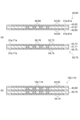
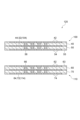
- 2A and 2B are cross-sectional views showing a method for manufacturing the semiconductor device shown in FIG. 3A to 3C are cross-sectional views showing a method for manufacturing the semiconductor device shown in FIG. 1, illustrating a step carried out after the step shown in FIG.
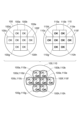
- FIG. 4 is a diagram for explaining a bonding process that reflects the results of the inspection process.
- FIG. 5 is a diagram for explaining a bonding process that reflects the results of the inspection process.
- FIG. 6 is a perspective view for explaining the bonding process of FIG. 4 and FIG.
- the term “layer” includes structures that are formed over the entire surface when viewed in a plan view, as well as structures that are formed on only a portion of the surface.
- the term “process” includes not only independent processes, but also processes that cannot be clearly distinguished from other processes as long as the intended effect of the process is achieved.
- a numerical range indicated using “ ⁇ ” indicates a range that includes the numerical values before and after " ⁇ " as the minimum and maximum values, respectively.
- the upper or lower limit of a numerical range in one stage may be replaced with the upper or lower limit of a numerical range in another stage.
- the upper or lower limit of the numerical range may be replaced with a value shown in the examples.
- the semiconductor device 1 (corresponding to the third laminated wafer 120) is a three-dimensional laminate in which four semiconductor wafers are laminated.
- the semiconductor device 1 has five layers of wiring electrodes 11 to 15, five layers of insulating layers 21 to 25, and semiconductor substrates 31 to 34.
- the wiring electrode 11 is formed in the insulating layer 21, and the wiring electrode 12 is formed in the insulating layer 22.
- the wiring electrode 13 is formed in the insulating layer 23.
- the wiring electrode 14 is formed in the insulating layer 24.
- the wiring electrode 15 is formed in the insulating layer 25.
- Each of the semiconductor substrates 31 to 34 is, for example, a silicon wafer, and corresponds to the semiconductor substrates 41, 51, 61, and 71 described later (see FIG. 2).
- the semiconductor device 1 shown in FIG. 1 shows an example in which, for example, four layers of semiconductor wafers are laminated, but is not limited thereto, and may be a laminate in which a multi-layer semiconductor wafer (for example, eight layers of semiconductor wafers or sixteen layers of semiconductor wafers) is further laminated.
- the semiconductor device 1 is further provided with through electrodes 36-39 that penetrate each semiconductor wafer.
- the through electrode 36 penetrates the semiconductor substrate 31 to connect the wiring electrode 11 and the wiring electrode 12.
- the through electrode 37 penetrates the semiconductor substrate 32 to connect the wiring electrode 12 and the wiring electrode 13.
- the through electrode 38 penetrates the semiconductor substrate 33 to connect the wiring electrode 13 and the wiring electrode 14.
- the through electrode 39 penetrates the semiconductor substrate 34 to connect the wiring electrode 14 and the wiring electrode 15.
- Each of the through electrodes 36-39 is, for example, a through silicon electrode (Through Silicon Via, TSV).
- each of the through electrodes 36-39 may be configured to directly connect the corresponding wiring electrodes, or may be configured to connect the corresponding wiring electrodes as wiring including two or more through electrodes and electrodes connecting them.
- Figures 2(a) and 2(b) are cross-sectional views showing a method for manufacturing the semiconductor device shown in Figure 1.
- Figure 3 is a cross-sectional view showing a method for manufacturing the semiconductor device shown in Figure 1, showing a step carried out after the step shown in Figure 2. This manufacturing method includes the following steps [A] to [G].
- Step A A step of preparing a first semiconductor wafer having a first semiconductor substrate, a first electrode provided on a first surface of the first semiconductor substrate, a second electrode provided on a second surface of the first semiconductor substrate, and wiring including a first through electrode that penetrates the first semiconductor substrate and connects the first electrode and the second electrode to each other.
- Step B A step of preparing a second semiconductor wafer having a second semiconductor substrate, a third electrode provided on a first surface of the second semiconductor substrate, a fourth electrode provided on a second surface of the second semiconductor substrate, and wiring including a second through electrode that penetrates the second semiconductor substrate and connects the third electrode and the fourth electrode to each other.
- Step C A step of preparing a third semiconductor wafer having a third semiconductor substrate, a fifth electrode provided on a first surface of the third semiconductor substrate, a sixth electrode provided on a second surface of the third semiconductor substrate, and wiring including a third through electrode that penetrates the third semiconductor substrate and connects the fifth electrode and the sixth electrode to each other.
- Step D A step of preparing a fourth semiconductor wafer having a fourth semiconductor substrate, a seventh electrode provided on a first surface of the fourth semiconductor substrate, an eighth electrode provided on a second surface of the fourth semiconductor substrate, and wiring including a fourth through electrode that penetrates the fourth semiconductor substrate and connects the seventh electrode and the eighth electrode to each other.
- Step E A step of stacking and integrating the first semiconductor wafer and the second semiconductor wafer, and connecting the second electrode and the third electrode to produce a first laminated wafer.
- Step F A step of stacking and integrating the third semiconductor wafer and the fourth semiconductor wafer, and connecting the sixth electrode and the seventh electrode to produce a second laminated wafer.
- Step G A step of stacking and integrating the first and second laminated wafers together and connecting the fourth electrode and the fifth electrode to produce a third laminated wafer.
- a first semiconductor wafer 40 is prepared.
- the first semiconductor wafer 40 has a semiconductor substrate 41 (first semiconductor substrate), a plurality of electrodes 42 (first electrodes) provided on a first surface 41a of the semiconductor substrate 41, an insulating layer 43 (first insulating layer) provided on the first surface 41a of the semiconductor substrate 41, a plurality of electrodes 44 (second electrodes) provided on a second surface 41b of the semiconductor substrate 41, an insulating layer 45 (second insulating layer) provided on the second surface 41b of the semiconductor substrate 41, and wiring including a through electrode 46 (first through electrode) that penetrates the semiconductor substrate 41 and connects the electrodes 42 and 44 to each other.
- a through electrode 46 first through electrode
- a semiconductor substrate 41 is prepared, which is a silicon substrate on which an integrated circuit consisting of semiconductor elements and wiring connecting the elements is formed.
- the thickness of this semiconductor substrate 41 is, for example, 4 ⁇ m to 775 ⁇ m.
- holes are then provided through the semiconductor substrate 41 by a specified method, and a plurality of through electrodes 46 are formed to fill the holes.
- the through electrodes 46 are so-called TSVs, and a known method such as the Bosch process (Non-Patent Document 6) can be used to form them.
- a plurality of electrodes 42 that will become the wiring electrodes 11 and an insulating layer 43 that will become the insulating layer 21 are formed on the first surface 41a of the semiconductor substrate 41 made of silicon or the like.
- Each electrode 42 can be formed by a method such as providing a resist opening and depositing a conductive material such as copper in the opening by electroplating.
- the insulating layer 43 is formed, for example, from an organic insulating material.
- the insulating layer 43 can be formed by applying liquid polyimide (PI) by spin coating onto the first surface 41a of the semiconductor substrate 41 on which the electrodes 42 are formed, and then curing the liquid.
- the electrodes 42 and the insulating layer 43 may be formed using other methods.
- the thickness of the electrodes 42 and the insulating layer 43 is, for example, 1 ⁇ m or more and 10 ⁇ m or less.
- the organic insulating material used for the insulating layer 43 may be, other than polyimide, a polyimide precursor (e.g., polyimide ester or polyamic acid), polyamideimide, bismaleimide, benzocyclobutene (BCB), polybenzoxazole (PBO), or a PBO precursor.
- a polyimide precursor e.g., polyimide ester or polyamic acid
- polyamideimide e.g., polyamideimide, bismaleimide, benzocyclobutene (BCB), polybenzoxazole (PBO), or a PBO precursor.
- BCB benzocyclobutene
- PBO polybenzoxazole
- PBO polybenzoxazole
- the insulating layer 43 may be formed from an inorganic material such as silicon oxide.
- a plurality of electrodes 44 that will become part of the wiring electrodes 12 and an insulating layer 45 that will become part of the insulating layer 22 are formed on the second surface 41b of the semiconductor substrate 41 made of silicon or the like.
- the method of forming the electrodes 44 and the insulating layer 45 can be the same as the method of forming the electrodes 42 and the insulating layer 43 described above, so a description thereof will be omitted.
- the first semiconductor wafer 40 is formed.
- the electrodes 42 and 44 are directly connected by the through electrodes 46, but the electrodes 42 and 44 may be connected by wiring including a plurality of through electrodes and electrodes connecting them. The same may be true for the other semiconductor wafers described below.
- a second semiconductor wafer 50 is prepared.
- the second semiconductor wafer 50 has a semiconductor substrate 51 (second semiconductor substrate), a plurality of electrodes 52 (third electrodes) provided on the first surface 51a of the semiconductor substrate 51, an insulating layer 53 (third insulating layer) provided on the first surface 51a of the semiconductor substrate 51, a plurality of electrodes 54 (fourth electrodes) provided on the second surface 51b of the semiconductor substrate 51, an insulating layer 55 (fourth insulating layer) provided on the second surface 51b of the semiconductor substrate 51, and wiring including a plurality of through electrodes 56 (second through electrodes) that penetrate the semiconductor substrate 51 and connect the electrodes 52 and 54 to each other.
- step B the materials and forming methods of the electrodes 52 and 54, the insulating layers 53 and 55, and the through electrodes 56 in the second semiconductor wafer 50 are the same as those of the first semiconductor wafer 40, so detailed description will be omitted.
- the insulating layer 53 constitutes a part of the insulating layer 22.
- the electrodes 54 on the second semiconductor wafer 50 constitute a part of the wiring electrodes 13 on the semiconductor device 1 shown in FIG. 1
- the insulating layer 55 constitutes a part of the insulating layer 23.
- a third semiconductor wafer 60 is prepared.
- the third semiconductor wafer 60 has a semiconductor substrate 61 (third semiconductor substrate), a plurality of electrodes 62 (fifth electrodes) provided on the first surface 61a of the semiconductor substrate 61, an insulating layer 63 (fifth insulating layer) provided on the first surface 61a of the semiconductor substrate 61, a plurality of electrodes 64 (sixth electrodes) provided on the second surface 61b of the semiconductor substrate 61, an insulating layer 65 (sixth insulating layer) provided on the second surface 61b of the semiconductor substrate 61, and wiring including a plurality of through electrodes 66 (third through electrodes) that penetrate the semiconductor substrate 61 and connect the electrodes 62 and 64 to each other.
- step C the materials and forming methods of the electrodes 62 and 64, the insulating layers 63 and 65, and the through electrodes 66 in the third semiconductor wafer 60 are the same as those of the first semiconductor wafer 40, etc., so detailed description will be omitted.
- the electrode 62 in the third semiconductor wafer 60 constitutes a part of the wiring electrode 13
- the insulating layer 63 constitutes a part of the insulating layer 23.
- the electrode 64 in the third semiconductor wafer 60 constitutes a part of the wiring electrode 14
- the insulating layer 65 constitutes a part of the insulating layer 24, of the semiconductor device 1 shown in FIG.
- a fourth semiconductor wafer 70 is prepared.
- the fourth semiconductor wafer 70 has a semiconductor substrate 71 (fourth semiconductor substrate), a plurality of electrodes 72 (seventh electrodes) provided on the first surface 71a of the semiconductor substrate 71, an insulating layer 73 (seventh insulating layer) provided on the first surface 71a of the semiconductor substrate 71, a plurality of electrodes 74 (eighth electrodes) provided on the second surface 71b of the semiconductor substrate 71, an insulating layer 75 (eighth insulating layer) provided on the second surface 71b of the semiconductor substrate 71, and wiring including a plurality of through electrodes 76 (fourth through electrodes) that penetrate the semiconductor substrate 71 and connect the electrodes 72 and 74 to each other.
- step D the materials and forming methods of the electrodes 72 and 74, the insulating layers 73 and 75, and the through electrodes 76 in the fourth semiconductor wafer 70 are the same as those of the first semiconductor wafer 40, etc., so detailed description will be omitted.
- the electrode 72 in the fourth semiconductor wafer 70 constitutes a part of the wiring electrode 14
- the insulating layer 73 constitutes a part of the insulating layer 24.
- the electrode 74 in the fourth semiconductor wafer 70 constitutes the wiring electrode 15, and the insulating layer 75 constitutes the insulating layer 25, of the semiconductor device 1 shown in FIG.
- step E As shown in (a) and (b) of FIG. 2, when the preparation of the first semiconductor wafer 40 and the second semiconductor wafer 50 is completed, the first semiconductor wafer 40 and the second semiconductor wafer 50 are stacked and integrated, and each electrode 44 and each electrode 52 are connected to produce the first stacked wafer 100. That is, the first semiconductor wafer 40 and the second semiconductor wafer 50 are heated and pressurized to be integrated by hybrid bonding.
- the heating temperature for the first semiconductor wafer 40 and the second semiconductor wafer 50 is, for example, 150°C to 400°C, and the pressure is 0.04 MPa to 10 MPa.
- the insulating layer 45 of the first semiconductor wafer 40 and the insulating layer 53 of the second semiconductor wafer 50 are firmly bonded (connected), and each electrode 44 of the first semiconductor wafer 40 and each electrode 52 of the second semiconductor wafer are firmly bonded (connected).
- the electrode 44 and the electrode 52 are joined to form an electrode 104 shown in Fig. 2B.
- the electrode 104 is connected to both the through electrodes 46 and 56, and electrically connects the electrode 42 and the electrode 54.
- the electrode 104 corresponds to the wiring electrode 12 shown in Fig. 1.
- step F As shown in (a) and (b) of FIG. 2, when the preparation of the third semiconductor wafer 60 and the fourth semiconductor wafer 70 is completed, the third semiconductor wafer 60 and the fourth semiconductor wafer 70 are stacked and integrated, and the electrodes 64 and the electrodes 72 are connected to each other to produce the second stacked wafer 110. That is, the third semiconductor wafer 60 and the fourth semiconductor wafer 70 are heated and pressurized to be integrated by hybrid bonding.
- the heating temperature for the third semiconductor wafer 60 and the fourth semiconductor wafer 70 is, for example, 150°C to 400°C, and the pressure is 0.04 MPa to 10 MPa.
- the insulating layer 65 of the third semiconductor wafer 60 and the insulating layer 73 of the fourth semiconductor wafer 70 are firmly bonded (connected), and the electrodes 64 of the third semiconductor wafer 60 and the electrodes 72 of the fourth semiconductor wafer 70 are firmly bonded (connected).
- the electrode 64 and the electrode 72 are joined to form an electrode 114 shown in Fig. 2B.
- the electrode 114 is connected to both the through electrodes 66 and 76, and electrically connects the electrode 62 and the electrode 74.
- the electrode 114 corresponds to the wiring electrode 14 shown in Fig. 1.
- step G As shown in FIG. 3, when the preparation of the first laminated wafer 100 and the second laminated wafer 110 is completed, the first laminated wafer 100 and the second laminated wafer 110 are laminated and integrated, and the electrodes 54 and the electrodes 62 are connected to produce the third laminated wafer 120. That is, the first laminated wafer 100 and the second laminated wafer 110 are heated and pressurized to integrate the two by hybrid bonding.
- the heating temperature for the first laminated wafer 100 and the second laminated wafer 110 is, for example, 150° C. to 400° C., and the pressure is 0.04 MPa to 10 MPa.
- the insulating layer 55 of the first laminated wafer 100 and the insulating layer 63 of the second laminated wafer 110 are firmly bonded (connected), and the electrodes 54 of the first laminated wafer 100 and the electrodes 62 of the second laminated wafer 110 are firmly bonded (connected).
- the electrode 54 and the electrode 62 are joined to form the wiring electrode 13 shown in Fig. 1.
- the wiring electrode 13 is connected to both of the through electrodes 56 and 66, and the electrodes 42, 44, 52, 54, 62, 64, 72, and 74 are electrically connected to one another.
- a semiconductor device 1 is formed, which is a laminate in which four semiconductor wafers are stacked (see also FIG. 1).
- the semiconductor device 1 may be singulated to chip size by dicing or the like to obtain a large number of laminated semiconductor chips (at least one laminated semiconductor chip).
- the singulated laminated semiconductor chips can be mounted on another semiconductor substrate or the like to form a semiconductor device.
- the method for manufacturing a semiconductor device first, the first semiconductor wafer 40 and the second semiconductor wafer 50 are stacked together to produce the first laminated wafer 100, and then the third semiconductor wafer 60 and the fourth semiconductor wafer 70 are stacked together to produce the second laminated wafer 110.
- the first laminated wafer 100 and the second laminated wafer 110 are then stacked together to produce the multi-layered third laminated wafer 120.
- the number of layers can be multiplied in increments, and therefore the time required to manufacture a multi-layered semiconductor device can be shortened compared to a method in which layers are stacked one by one in sequence.
- the first surface 41a of the semiconductor substrate 41 is provided with an insulating layer 43
- the second surface 41b of the semiconductor substrate 41 is provided with an insulating layer 45
- the first surface 51a of the semiconductor substrate 51 is provided with an insulating layer 53
- the second surface 51b of the semiconductor substrate 51 is provided with an insulating layer 55.
- the insulating layer 45 and the insulating layer 53 are bonded and integrated, and the electrode 44 and the electrode 52 are bonded by applying heat and pressure.
- This allows the so-called hybrid bonding method to be used when stacking and integrating the first semiconductor wafer 40 and the second semiconductor wafer 50. This allows fine electrodes to be bonded to each other, and also makes it possible to reduce the height of the laminate.
- the first surface 61a of the semiconductor substrate 61 is further provided with an insulating layer 63
- the second surface 61b of the semiconductor substrate 61 is further provided with an insulating layer 65
- the first surface 71a of the semiconductor substrate 71 is further provided with an insulating layer 73
- the second surface 71b of the semiconductor substrate 71 is further provided with an insulating layer 75.
- the insulating layer 65 and the insulating layer 73 are bonded and integrated by applying heat and pressure, and the electrode 64 and the electrode 72 are bonded.
- the insulating layer 55 and the insulating layer 63 are bonded and integrated by applying heat and pressure, and the electrode 54 and the electrode 62 are bonded.
- a so-called hybrid bonding method can be used. This makes it possible to bond fine electrodes together and also to reduce the height of the laminate.
- each of the insulating layers 43, 45, 53, 55, 63, 65, 73, and 75 contains an organic insulating material. This allows the organic insulating material to absorb any debris that adheres to the bonding surface during hybrid bonding, reducing bonding defects. If each of the insulating layers 43, 45, 53, 55, 63, 65, 73, and 75 contains an inorganic insulating material, it becomes easier to form fine insulating layers and electrodes.
- the organic insulating material constituting each of the insulating layers 43, 45, 53, 55, 63, 65, 73, and 75 preferably contains bismaleimide, polyimide, polyimide precursor, polyamideimide, benzocyclobutene (BCB), polybenzoxazole (PBO), or a PBO precursor.
- BCB benzocyclobutene
- PBO polybenzoxazole
- the present invention is not limited to the above-mentioned embodiments, and appropriate modifications may be made within the scope of the present disclosure.
- the stacking and bonding of semiconductor wafers and stacking and bonding of stacked semiconductor wafers are performed by hybrid bonding, but the present invention is not limited to this.
- the electrode 44 and the electrode 52 may be bonded by a solder bump. This method can also reliably bond the electrode 44 and the electrode 52.
- solder bump bonding using NCF Non Conductive Film
- underfill may be injected between the wafers in which the electrodes are bonded to each other to fix them.
- the electrodes may be bonded by a solder bump in the same manner.
- each semiconductor wafer is laminated and bonded as a unit. Therefore, in the manufacturing method of a semiconductor device according to this embodiment, before producing a wafer laminate (for example, before laminating the first laminated wafer 100 and the second laminated wafer 110 as shown in FIG. 6), a continuity test may be performed on the semiconductor chip areas 100a-100h (plurality of first semiconductor chip areas) and the semiconductor chip areas 110a-110h (plurality of second semiconductor chip areas) included in each laminated wafer, as shown in FIG. 4.
- each laminated wafer is a large-sized wafer including a plurality of semiconductor chip areas (areas that become semiconductor chips when each is singulated), and the continuity test is performed by inspecting the continuity and insulation of each semiconductor chip area from both sides of the laminated wafer with a fraying probe or the like. If the result of the continuity test indicates that there is a semiconductor chip area that is determined to be defective (Fail) (see FIG. 5), the overall yield rate (yield) can be improved by not manufacturing the part or not using the substrate. 4 shows a case where all semiconductor chip regions are good (OK), and FIG. 5 shows a case where some wiring parts are defective (Fail). In the example of FIG.
- the semiconductor chip regions judged to be good are selected to be overlapped with each other, and for example, semiconductor chip regions 100d, 110d, semiconductor chip regions 100e, 110e, semiconductor chip regions 100f, 110f, and semiconductor chip regions 100g, 110g are used as subsequent products, while the other semiconductor chip regions are not used in subsequent manufacturing.
- a plurality of first laminated wafers 100 and a plurality of second laminated wafers 110 may be prepared, and combinations of the first laminated wafers 100 and the second laminated wafers 110 may be selected so that the number of combinations in which the semiconductor chip regions are judged to be good products as a whole is increased.
- one first laminated wafer 100 and one second laminated wafer 110 are simply combined, so that the number of semiconductor chip regions that are good products in the combination is limited to four.
- the rate of combinations of good products can be increased, and the overall quality rate of combinations can be increased.
- This selection process may be performed by calculating the quality rate (yield) of all semiconductor wafers and laminated semiconductor wafers combined using a computer, or other processing methods may be used. In this way, by excluding defective semiconductor wafers or semiconductor wafers with a high defect rate and proceeding to the next process with good semiconductor wafers or semiconductor wafers with a high quality rate, the quality rate of semiconductor devices can be improved overall.
- the third laminated wafer 120 thus produced through inspection is to be further laminated, a continuity test may be performed in advance, and the optimal combination may be selected and laminated based on the test results.
- the above-mentioned inspection process and selection process of good products have been described using the example of bonding the first laminated wafer 100 and the second laminated wafer 110, but this is not limited to this, and they may of course also be applied when bonding the first semiconductor wafer 40 and the second semiconductor wafer 50, or when bonding the third semiconductor wafer 60 and the fourth semiconductor wafer 70. By performing such inspection and selection processes, it is possible to reliably improve the rate of good products.
- 1...semiconductor device (third laminated wafer), 40...first semiconductor wafer, 41...semiconductor substrate (first semiconductor substrate), 41a...first surface, 41b...second surface, 42...electrode (first electrode), 43...insulating layer (first insulating layer), 44...electrode (second electrode), 45...insulating layer (second insulating layer), 46...through electrode (first through electrode), 50...second semiconductor wafer, 51...semiconductor substrate (second semiconductor substrate), 51a...first surface, 51b...second surface, 52...electrode (third electrode), 53...insulating layer (third insulating layer), 54...electrode (fourth electrode), 55...insulating layer (fourth insulating layer), 56...through electrode (second through electrode), 60...third semiconductor wafer Eha, 61...semiconductor substrate (third semiconductor substrate), 61a...first surface, 61b...second surface, 62...electrode (fifth electrode), 63...insulating layer (fifth insulating
Landscapes
- Internal Circuitry In Semiconductor Integrated Circuit Devices (AREA)
Abstract
Description
工程B:第2半導体基板と、第2半導体基板の第1面に設けられた第3電極と、第2半導体基板の第2面に設けられた第4電極と、第2半導体基板を貫通し第3電極及び第4電極を互いに接続する、第2貫通電極を含む配線とを有する第2半導体ウエハを準備する工程。
工程C:第3半導体基板と、第3半導体基板の第1面に設けられた第5電極と、第3半導体基板の第2面に設けられた第6電極と、第3半導体基板を貫通し第5電極及び第6電極を互いに接続する、第3貫通電極を含む配線とを有する第3半導体ウエハを準備する工程。
工程D:第4半導体基板と、第4半導体基板の第1面に設けられた第7電極と、第4半導体基板の第2面に設けられた第8電極と、第4半導体基板を貫通し第7電極及び第8電極を互いに接続する、第4貫通電極を含む配線とを有する第4半導体ウエハを準備する工程。
工程E:第1半導体ウエハと第2半導体ウエハとを積層して一体化すると共に、第2電極と第3電極とを接続して第1積層ウエハを作製する工程。
工程F:第3半導体ウエハと第4半導体ウエハとを積層して一体化すると共に、第6電極と第7電極とを接続して第2積層ウエハを作製する工程。
工程G:第1積層ウエハと第2積層ウエハとを積層して一体化すると共に、第4電極と第5電極とを接続して第3積層ウエハを作製する工程。
工程Aでは、図2の(a)に示すように、第1半導体ウエハ40を準備する。第1半導体ウエハ40は、半導体基板41(第1半導体基板)と、半導体基板41の第1面41aに設けられた複数の電極42(第1電極)と、半導体基板41の第1面41aに設けられた絶縁層43(第1絶縁層)と、半導体基板41の第2面41bに設けられた複数の電極44(第2電極)と、半導体基板41の第2面41bに設けられた絶縁層45(第2絶縁層)と、半導体基板41を貫通し、電極42,44を互いに接続する、貫通電極46(第1貫通電極)を含む配線と、を有している。
工程Bでは、第2半導体ウエハ50を準備する。第2半導体ウエハ50は、半導体基板51(第2半導体基板)と、半導体基板51の第1面51aに設けられた複数の電極52(第3電極)と、半導体基板51の第1面51aに設けられた絶縁層53(第3絶縁層)と、半導体基板51の第2面51bに設けられた複数の電極54(第4電極)と、半導体基板51の第2面51bに設けられた絶縁層55(第4絶縁層)と、半導体基板51を貫通し、電極52,54を互いに接続する、複数の貫通電極56(第2貫通電極)を含む配線と、を有している。工程Bにおいて、第2半導体ウエハ50における電極52,54、絶縁層53,55及び貫通電極56の材料及び形成方法は、第1半導体ウエハ40と同様であるため、詳細な説明は省略する。なお、第2半導体ウエハ50における各電極52は、図1に示す半導体装置1の配線電極12の一部を構成し、絶縁層53は、絶縁層22の一部を構成する。また、第2半導体ウエハ50における電極54は、図1に示す半導体装置1の配線電極13の一部を構成し、絶縁層55は、絶縁層23の一部を構成する。
工程Cでは、第3半導体ウエハ60を準備する。第3半導体ウエハ60は、半導体基板61(第3半導体基板)と、半導体基板61の第1面61aに設けられた複数の電極62(第5電極)と、半導体基板61の第1面61aに設けられた絶縁層63(第5絶縁層)と、半導体基板61の第2面61bに設けられた複数の電極64(第6電極)と、半導体基板61の第2面61bに設けられた絶縁層65(第6絶縁層)と、半導体基板61を貫通し、電極62,64を互いに接続する、複数の貫通電極66(第3貫通電極)を含む配線と、を有している。工程Cにおいて、第3半導体ウエハ60における電極62,64、絶縁層63,65及び貫通電極66の材料及び形成方法は、第1半導体ウエハ40等と同様であるため、詳細な説明は省略する。なお、第3半導体ウエハ60における電極62は、図1に示す半導体装置1の配線電極13の一部を構成し、絶縁層63は、絶縁層23の一部を構成する。また、第3半導体ウエハ60における電極64は、図1に示す半導体装置1の配線電極14の一部を構成し、絶縁層65は、絶縁層24の一部を構成する。
工程Dでは、第4半導体ウエハ70を準備する。第4半導体ウエハ70は、半導体基板71(第4半導体基板)と、半導体基板71の第1面71aに設けられた複数の電極72(第7電極)と、半導体基板71の第1面71aに設けられた絶縁層73(第7絶縁層)と、半導体基板71の第2面71bに設けられた複数の電極74(第8電極)と、半導体基板71の第2面71bに設けられた絶縁層75(第8絶縁層)と、半導体基板71を貫通し、電極72,74を互いに接続する、複数の貫通電極76(第4貫通電極)を含む配線と、を有している。工程Dにおいて、第4半導体ウエハ70における電極72,74、絶縁層73,75及び貫通電極76の材料及び形成方法は、第1半導体ウエハ40等と同様であるため、詳細な説明は省略する。なお、第4半導体ウエハ70における電極72は、図1に示す半導体装置1の配線電極14の一部を構成し、絶縁層73は、絶縁層24の一部を構成する。また、第4半導体ウエハ70における電極74は、図1に示す半導体装置1の配線電極15を構成し、絶縁層75は、絶縁層25を構成する。
工程Eでは、図2の(a)及び(b)に示すように、第1半導体ウエハ40及び第2半導体ウエハ50の準備が終了すると、第1半導体ウエハ40と第2半導体ウエハ50とを積層して一体化すると共に、各電極44と各電極52とを接続して第1積層ウエハ100を作製する。即ち、第1半導体ウエハ40と第2半導体ウエハ50とに対して加熱及び加圧を付与して、ハイブリッド接合によって両者を一体化する。第1半導体ウエハ40及び第2半導体ウエハ50に対する加熱温度は、例えば150℃~400℃であり、加圧は、0.04MPa~10MPaである。このような接合によって、第1半導体ウエハ40の絶縁層45と第2半導体ウエハ50の絶縁層53とが強固に接合(接続)されると共に、第1半導体ウエハ40の各電極44と第2半導体ウエハの各電極52とが強固に接合(接続)される。電極44と電極52とが接合されて、図2の(b)に示す電極104が形成される。電極104は、貫通電極46,56の両方に接続され、電極42と電極54とを電気的に接続する。電極104は、図1に示す配線電極12に対応する。
工程Fでは、図2の(a)及び(b)に示すように、第3半導体ウエハ60及び第4半導体ウエハ70の準備が終了すると、第3半導体ウエハ60と第4半導体ウエハ70とを積層して一体化すると共に、各電極64と各電極72とを接続して第2積層ウエハ110を作製する。即ち、第3半導体ウエハ60と第4半導体ウエハ70とに対して加熱及び加圧を付与して、ハイブリッド接合によって両者を一体化する。第3半導体ウエハ60及び第4半導体ウエハ70に対する加熱温度は、例えば150℃~400℃であり、加圧は、0.04MPa~10MPaである。このような接合によって、第3半導体ウエハ60の絶縁層65と第4半導体ウエハ70の絶縁層73とが強固に接合(接続)されると共に、第3半導体ウエハ60の各電極64と第4半導体ウエハ70の各電極72とが強固に接合(接続)される。電極64と電極72とが接合されて、図2の(b)に示す電極114が形成される。電極114は、貫通電極66,76の両方に接続され、電極62と電極74とを電気的に接続する。電極114は、図1に示す配線電極14に対応する。
工程Gでは、図3に示すように、第1積層ウエハ100及び第2積層ウエハ110の準備が終了すると、第1積層ウエハ100と第2積層ウエハ110とを積層して一体化すると共に、各電極54と各電極62とを接続して第3積層ウエハ120を作製する。即ち、第1積層ウエハ100と第2積層ウエハ110とに対して加熱及び加圧を付与して、ハイブリッド接合によって両者を一体化する。第1積層ウエハ100及び第2積層ウエハ110に対する加熱温度は、例えば150℃~400℃であり、加圧は、0.04MPa~10MPaである。このような接合によって、第1積層ウエハ100の絶縁層55と第2積層ウエハ110の絶縁層63とが強固に接合(接続)されると共に、第1積層ウエハ100の各電極54と第2積層ウエハ110の各電極62とが強固に接合(接続)される。電極54と電極62とが接合されて、図1に示す配線電極13が形成される。配線電極13は、貫通電極56,66の両方に接続され、電極42,44,52,54,62,64,72,74が相互に電気的に接続される。
Claims (12)
- 第1半導体基板と、前記第1半導体基板の第1面に設けられた第1電極と、前記第1半導体基板の第2面に設けられた第2電極と、前記第1半導体基板を貫通し前記第1電極及び前記第2電極を互いに接続する、第1貫通電極を含む配線とを有する第1半導体ウエハを準備する工程と、
第2半導体基板と、前記第2半導体基板の第1面に設けられた第3電極と、前記第2半導体基板の第2面に設けられた第4電極と、前記第2半導体基板を貫通し前記第3電極及び前記第4電極を互いに接続する、第2貫通電極を含む配線とを有する第2半導体ウエハを準備する工程と、
第3半導体基板と、前記第3半導体基板の第1面に設けられた第5電極と、前記第3半導体基板の第2面に設けられた第6電極と、前記第3半導体基板を貫通し前記第5電極及び前記第6電極を互いに接続する、第3貫通電極を含む配線とを有する第3半導体ウエハを準備する工程と、
第4半導体基板と、前記第4半導体基板の第1面に設けられた第7電極と、前記第4半導体基板の第2面に設けられた第8電極と、前記第4半導体基板を貫通し前記第7電極及び前記第8電極を互いに接続する、第4貫通電極を含む配線とを有する第4半導体ウエハを準備する工程と、
前記第1半導体ウエハと前記第2半導体ウエハとを積層して一体化すると共に、前記第2電極と前記第3電極とを接続して第1積層ウエハを作製する工程と、
前記第3半導体ウエハと前記第4半導体ウエハとを積層して一体化すると共に、前記第6電極と前記第7電極とを接続して第2積層ウエハを作製する工程と、
前記第1積層ウエハと前記第2積層ウエハとを積層して一体化すると共に、前記第4電極と前記第5電極とを接続して第3積層ウエハを作製する工程と、
を備える、半導体装置の製造方法。 - 前記第1半導体基板の前記第1面には第1絶縁層が設けられると共に、前記第1半導体基板の前記第2面には第2絶縁層が設けられ、
前記第2半導体基板の前記第1面には第3絶縁層が設けられると共に、前記第2半導体基板の前記第2面には第4絶縁層が設けられ、
前記第1積層ウエハを作製する工程では、加熱及び加圧の少なくとも一方を付与することにより、前記第2絶縁層と前記第3絶縁層とを接合して一体化すると共に前記第2電極と前記第3電極とを接合する、
請求項1に記載の半導体装置の製造方法。 - 前記第3半導体基板の前記第1面には第5絶縁層が設けられると共に、前記第3半導体基板の前記第2面には第6絶縁層が設けられ、
前記第4半導体基板の前記第1面には第7絶縁層が設けられると共に、前記第4半導体基板の前記第2面には第8絶縁層が設けられ、
前記第2積層ウエハを作製する工程では、加熱及び加圧の少なくとも一方を付与することにより、前記第6絶縁層と前記第7絶縁層とを接合して一体化すると共に前記第6電極と前記第7電極とを接合し、
前記第3積層ウエハを作製する工程では、加熱及び加圧の少なくとも一方を付与することにより、前記第4絶縁層と前記第5絶縁層とを接合して一体化すると共に前記第4電極と前記第5電極とを接合する、
請求項2に記載の半導体装置の製造方法。 - 前記第1絶縁層、前記第2絶縁層、前記第3絶縁層、及び前記第4絶縁層は、有機絶縁材料及び無機絶縁材料の少なくとも一方を含む、
請求項2又は3に記載の半導体装置の製造方法。 - 前記有機絶縁材料は、ビスマレイミド、ポリイミド、ポリイミド前駆体、ポリアミドイミド、ベンゾシクロブテン(BCB)、ポリベンゾオキサゾール(PBO)、又は、PBO前駆体を含む、
請求項4に記載の半導体装置の製造方法。 - 前記第1積層ウエハを作製する工程では、前記第2電極と前記第3電極とを半田バンプによって接合する、
請求項1に記載の半導体装置の製造方法。 - 前記第1積層ウエハ及び前記第2積層ウエハを、前記第3積層ウエハを作製する前に検査する工程を更に備える、
請求項1~6の何れか一項に記載の半導体装置の製造方法。 - 前記第1積層ウエハは、複数の第1半導体チップ領域を含み、
前記第2積層ウエハは、複数の第2半導体チップ領域を含み、
前記検査する工程では、前記複数の第1半導体チップ領域のそれぞれが検査されると共に、前記複数の第2半導体チップ領域のそれぞれが検査され、
前記第3積層ウエハを作製する工程では、前記検査する工程での検査結果に基づいて前記複数の第1半導体チップ領域それぞれと前記複数の第2半導体チップ領域それぞれとの組み合わせが選択される、
請求項7に記載の半導体装置の製造方法。 - 前記第3積層ウエハを作製する工程では、前記検査する工程で良品と判断された各半導体チップ領域同士が重ね合わされるように選択が行われる、
請求項8に記載の半導体装置の製造方法。 - 前記第3積層ウエハを作製する工程を2回以上行って複数の第3積層ウエハを作製する工程と、
前記複数の第3積層ウエハを積層して第4積層ウエハを作製する工程と、を更に備える、
請求項1~9の何れか一項に記載の半導体装置の製造方法。 - 前記第3積層ウエハを含む積層体をチップサイズに個片化し、少なくとも1つの積層半導体チップを得る工程を更に備える、
請求項1~10の何れか一項に記載の半導体装置の製造方法。 - 請求項11に記載の半導体装置の製造方法によって製造される少なくとも1つの積層半導体チップと、
前記積層半導体チップが実装される基板と、
を備える半導体装置。
Priority Applications (4)
| Application Number | Priority Date | Filing Date | Title |
|---|---|---|---|
| KR1020257043036A KR20260025322A (ko) | 2023-06-07 | 2023-06-07 | 반도체 장치의 제조 방법, 및, 반도체 장치 |
| JP2025525527A JPWO2024252561A1 (ja) | 2023-06-07 | 2023-06-07 | |
| CN202380097616.2A CN121014280A (zh) | 2023-06-07 | 2023-06-07 | 半导体装置的制造方法以及半导体装置 |
| PCT/JP2023/021165 WO2024252561A1 (ja) | 2023-06-07 | 2023-06-07 | 半導体装置の製造方法、及び、半導体装置 |
Applications Claiming Priority (1)
| Application Number | Priority Date | Filing Date | Title |
|---|---|---|---|
| PCT/JP2023/021165 WO2024252561A1 (ja) | 2023-06-07 | 2023-06-07 | 半導体装置の製造方法、及び、半導体装置 |
Publications (1)
| Publication Number | Publication Date |
|---|---|
| WO2024252561A1 true WO2024252561A1 (ja) | 2024-12-12 |
Family
ID=93795416
Family Applications (1)
| Application Number | Title | Priority Date | Filing Date |
|---|---|---|---|
| PCT/JP2023/021165 Ceased WO2024252561A1 (ja) | 2023-06-07 | 2023-06-07 | 半導体装置の製造方法、及び、半導体装置 |
Country Status (4)
| Country | Link |
|---|---|
| JP (1) | JPWO2024252561A1 (ja) |
| KR (1) | KR20260025322A (ja) |
| CN (1) | CN121014280A (ja) |
| WO (1) | WO2024252561A1 (ja) |
Citations (4)
| Publication number | Priority date | Publication date | Assignee | Title |
|---|---|---|---|---|
| JP2007036104A (ja) * | 2005-07-29 | 2007-02-08 | Nec Electronics Corp | 半導体装置およびその製造方法 |
| JP2012204653A (ja) * | 2011-03-25 | 2012-10-22 | Dainippon Printing Co Ltd | 半導体装置、半導体装置の製造方法 |
| US20160155724A1 (en) * | 2014-12-01 | 2016-06-02 | Taeyeong Kim | Semiconductor devices having stacked structures and methods for fabricating the same |
| JP2020068253A (ja) * | 2018-10-23 | 2020-04-30 | 株式会社ダイセル | 半導体装置製造方法 |
-
2023
- 2023-06-07 JP JP2025525527A patent/JPWO2024252561A1/ja active Pending
- 2023-06-07 CN CN202380097616.2A patent/CN121014280A/zh active Pending
- 2023-06-07 WO PCT/JP2023/021165 patent/WO2024252561A1/ja not_active Ceased
- 2023-06-07 KR KR1020257043036A patent/KR20260025322A/ko active Pending
Patent Citations (4)
| Publication number | Priority date | Publication date | Assignee | Title |
|---|---|---|---|---|
| JP2007036104A (ja) * | 2005-07-29 | 2007-02-08 | Nec Electronics Corp | 半導体装置およびその製造方法 |
| JP2012204653A (ja) * | 2011-03-25 | 2012-10-22 | Dainippon Printing Co Ltd | 半導体装置、半導体装置の製造方法 |
| US20160155724A1 (en) * | 2014-12-01 | 2016-06-02 | Taeyeong Kim | Semiconductor devices having stacked structures and methods for fabricating the same |
| JP2020068253A (ja) * | 2018-10-23 | 2020-04-30 | 株式会社ダイセル | 半導体装置製造方法 |
Also Published As
| Publication number | Publication date |
|---|---|
| KR20260025322A (ko) | 2026-02-24 |
| JPWO2024252561A1 (ja) | 2024-12-12 |
| CN121014280A (zh) | 2025-11-25 |
Similar Documents
| Publication | Publication Date | Title |
|---|---|---|
| JP7543712B2 (ja) | 半導体装置の製造方法 | |
| US11488878B2 (en) | Packaging mechanisms for dies with different sizes of connectors | |
| KR102506102B1 (ko) | 반도체 패키지 구조체 및 그 제조 방법 | |
| US7973310B2 (en) | Semiconductor package structure and method for manufacturing the same | |
| US9911725B2 (en) | Packaging mechanisms for dies with different sizes of connectors | |
| CN110620085A (zh) | 层叠封装接合结构及其形成方法 | |
| CN104299920A (zh) | 形成封装结构的机制 | |
| JP7501133B2 (ja) | 半導体装置の製造方法 | |
| US20230163102A1 (en) | Bonding structure and manufacturing method therefor | |
| US8518741B1 (en) | Wafer-to-wafer process for manufacturing a stacked structure | |
| CN114450785A (zh) | 一种多芯片堆叠封装及制作方法 | |
| Kayaba et al. | A new adhesive for CoW Cu-Cu hybrid bonding with high throughput and room temperature pre-bonding | |
| Hu et al. | Embedded glass interposer for heterogeneous multi-chip integration | |
| Derakhshandeh et al. | Low temperature backside damascene processing on temporary carrier wafer targeting 7μm and 5μm pitch microbumps for N equal and greater than 2 die to wafer TCB stacking | |
| WO2022203020A1 (ja) | 半導体装置の製造方法、半導体装置、集積回路要素、及び、集積回路要素の製造方法 | |
| KR20240021122A (ko) | 집적 회로 패키지 및 이의 형성 방법 | |
| TWI895978B (zh) | 半導體裝置與其形成方法 | |
| KR20260025322A (ko) | 반도체 장치의 제조 방법, 및, 반도체 장치 | |
| US12119238B2 (en) | Semiconductor bonding structures and methods | |
| Shen et al. | Process development and material characteristics of TSV-less interconnection technology for FOWLP | |
| JP5853759B2 (ja) | 半導体ベアチップ、半導体ベアチップ接合体、3次元積層半導体装置及びその製造方法 | |
| WO2023007629A1 (ja) | 半導体装置の製造方法、及び、半導体装置 | |
| JPWO2024252561A5 (ja) | ||
| TWI902262B (zh) | 三維半導體封裝元件及其製作方法 | |
| TWI862215B (zh) | 晶片封裝結構及其製作方法 |
Legal Events
| Date | Code | Title | Description |
|---|---|---|---|
| WWE | Wipo information: entry into national phase |
Ref document number: 18859551 Country of ref document: US |
|
| 121 | Ep: the epo has been informed by wipo that ep was designated in this application |
Ref document number: 23940664 Country of ref document: EP Kind code of ref document: A1 |
|
| ENP | Entry into the national phase |
Ref document number: 2025525527 Country of ref document: JP Kind code of ref document: A |
|
| WWE | Wipo information: entry into national phase |
Ref document number: 2025525527 Country of ref document: JP |
|
| NENP | Non-entry into the national phase |
Ref country code: DE |