WO2024252509A1 - 電力変換装置および電動車両 - Google Patents
電力変換装置および電動車両 Download PDFInfo
- Publication number
- WO2024252509A1 WO2024252509A1 PCT/JP2023/020929 JP2023020929W WO2024252509A1 WO 2024252509 A1 WO2024252509 A1 WO 2024252509A1 JP 2023020929 W JP2023020929 W JP 2023020929W WO 2024252509 A1 WO2024252509 A1 WO 2024252509A1
- Authority
- WO
- WIPO (PCT)
- Prior art keywords
- substrate
- power conversion
- conversion device
- core
- conversion element
- Prior art date
- Legal status (The legal status is an assumption and is not a legal conclusion. Google has not performed a legal analysis and makes no representation as to the accuracy of the status listed.)
- Ceased
Links
Images

Classifications
-
- H—ELECTRICITY
- H02—GENERATION; CONVERSION OR DISTRIBUTION OF ELECTRIC POWER
- H02M—APPARATUS FOR CONVERSION BETWEEN AC AND AC, BETWEEN AC AND DC, OR BETWEEN DC AND DC, AND FOR USE WITH MAINS OR SIMILAR POWER SUPPLY SYSTEMS; CONVERSION OF DC OR AC INPUT POWER INTO SURGE OUTPUT POWER; CONTROL OR REGULATION THEREOF
- H02M1/00—Details of apparatus for conversion
- H02M1/0003—Details of control, feedback or regulation circuits
- H02M1/0009—Devices or circuits for detecting current in a converter
-
- H—ELECTRICITY
- H02—GENERATION; CONVERSION OR DISTRIBUTION OF ELECTRIC POWER
- H02M—APPARATUS FOR CONVERSION BETWEEN AC AND AC, BETWEEN AC AND DC, OR BETWEEN DC AND DC, AND FOR USE WITH MAINS OR SIMILAR POWER SUPPLY SYSTEMS; CONVERSION OF DC OR AC INPUT POWER INTO SURGE OUTPUT POWER; CONTROL OR REGULATION THEREOF
- H02M7/00—Conversion of AC power input into DC power output; Conversion of DC power input into AC power output
- H02M7/003—Constructional details, e.g. physical layout, assembly, wiring or busbar connections
Definitions
- This application relates to a power conversion device and an electric vehicle.
- Electric vehicles that use a motor as a drive source are equipped with multiple power conversion devices.
- the power conversion devices are used to drive the motor or to regenerate drive energy to the battery.
- Specific power conversion devices include a charger that converts commercial AC power into DC power and charges the high-voltage battery, a DC/DC converter that converts the DC power of the high-voltage battery to the voltage of the battery for auxiliary equipment (e.g. 12V), and an inverter that converts DC power from the battery into AC power for the motor.
- the current sensor is composed of a bus bar, a C-shaped core made of a magnetic material, and a magnetoelectric conversion element, with the bus bar being placed inside the C-shaped core and the magnetoelectric conversion element being provided in the gap of the C-shaped core.
- the above-mentioned C-shaped core can be formed with a short gap length at the cutout, which enhances the magnetic collection effect on the magnetoelectric conversion element. For this reason, C-shaped cores are often used as magnetic cores that make up current sensors.
- the magnetoelectric conversion element is connected to a substrate and detects the magnetic flux generated in the cutout due to the current flowing through the bus bar.
- the core is equipped with a shielding section to reduce the influence of external magnetic fields on the magnetoelectric conversion element.
- the side portion of the C-shaped core extends opposite the bottom portion of the C-shaped core, and the current sensor and shield portion are integrally formed. This reduces the influence of external magnetic fields on the magnetoelectric conversion element while maintaining the high magnetic collection effect of the C-shaped core, making it possible to miniaturize the power conversion device.
- the present application therefore aims to obtain a power conversion device that can improve the positioning accuracy of the magnetoelectric conversion element relative to the gap portion of the core, thereby improving current detection accuracy, while maintaining the high magnetic collection effect of the core and the compact size of the power conversion device, and can reduce the influence of external magnetic fields on the gap portion of the core.
- the power conversion device disclosed in the present application is A substrate having a through hole; A bus bar connected to the power module and arranged to face the substrate; a core that is a cylinder having a notch and that surrounds the bus bar, the core having a pair of protrusions formed along the notch; a magnetoelectric conversion element disposed on the substrate and converting a detected magnetic field into an electric signal; Equipped with At least one of the pair of protrusions of the core is inserted into the through hole and fixed to the substrate; The magnetoelectric transducer is disposed in a notch portion of the core or in a gap between a pair of protrusions of the core. It is characterized by the above.
- the protruding portion of the core made of a magnetic material is inserted into one or more through holes provided in the substrate, and the magnetoelectric conversion element is disposed in a portion of the substrate adjacent to the through hole, so that the core maintains a high magnetic collection effect while also fulfilling the role of positioning with respect to the substrate. Therefore, it is possible to obtain a power conversion device that can improve the positioning accuracy of the magnetoelectric conversion element with respect to the gap portion of the core, thereby improving the current detection accuracy, and that can reduce the influence of external magnetic fields on the gap portion of the core.
- FIG. 1 is a schematic diagram showing a general configuration of a power conversion device according to a first embodiment; 1 is a perspective view showing a main part of a power conversion device according to a first embodiment. 1 is a front view showing a main part of a power conversion device according to a first embodiment. 2 is a front view for explaining a current sensor of the power conversion device according to the first embodiment. FIG. 2 is a front view for explaining a structure of a current sensor of the power conversion device according to the first embodiment.
- FIG. 11 is a plan view showing a main part of a power conversion device according to a second embodiment. FIG. 11 is a front view showing a main part of a power conversion device according to a second embodiment. FIG. FIG. FIG.
- FIG. 11 is a front view showing a main part of a power conversion device according to a third embodiment.
- FIG. 13 is a front view showing a main part of a power conversion device according to a fourth embodiment.
- FIG. 13 is a front view showing a main part of a power conversion device according to a fifth embodiment.
- Embodiment 1 A power conversion device 100 that converts electric power is mounted on a vehicle such as an electric vehicle or a hybrid vehicle that uses a motor as one of its drive sources.
- a vehicle such as an electric vehicle or a hybrid vehicle that uses a motor as one of its drive sources.
- the configuration of this power conversion device 100 will be outlined below with reference to FIG.
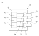
- FIG. 1 is a schematic diagram showing the general configuration of the power conversion device 100. This FIG. 1 also shows the power conversion device 100 as viewed from the underside of the substrate 50, which is a main component.
- bus bars 40a, 40b, 40c are configured to penetrate the inside of cores 10a, 10b, 10c, which have a notch at the top and a convex shape when viewed from the front, and which constitute current sensors 30a, 30b, 30c (these current sensors will be described in detail below) attached to the substrate 50 (the bus bars and convex cores will also be described in detail below), and are connected to power modules 70a, 70b, 70c provided in the power conversion device 100, respectively.
- the power modules 70a, 70b, and 70c have been described as being separate, but they may be integrated. Next, the configuration of the main parts of the power conversion device 100 will be described in detail with reference to Figures 2 to 5.
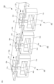
- FIG. 2 is a perspective view showing the main parts of the power conversion device 100 according to the first embodiment
- FIG. 3 is a front view showing the main parts of the power conversion device 100.
- FIG. 2 and FIG. 3 are views of the overall configuration of the power conversion device 100 with the housing surrounding the power conversion device 100 removed.
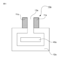
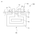
- FIG. 4 is a front view showing the current sensor 30a, which is a main part of the power conversion device 100 in FIG. 2
- FIG. 5 is a front view showing the convex-shaped core 10a, which is a main part of the current sensor 30a in FIG. 4.
- the power conversion device 100 includes three flat bus bars 40a, 40b, and 40c through which each phase of a three-phase current flows.
- a current sensor 30a is provided on the bus bar 40a
- a current sensor 30b is provided on the bus bar 40b
- a current sensor 30c is provided on the bus bar 40c.
- the bus bars 40a, 40b, and 40c have the same shape, and the current sensors 30a, 30b, and 30c have the same configuration, as described below.
- the power conversion device 100 also includes convex-shaped cores 10a, 10b, and 10c that constitute current sensors 30a, 30b, and 30c, and magnetoelectric conversion elements 20a, 20b, and 20c mounted on the surface of a substrate 50.
- each of the cores is a cylinder as a whole, has a notch, and a pair of columns (hereinafter also referred to as a pair of protrusions) are disposed facing each other toward the outside along the notch.
- the three bus bars 40a, 40b, and 40c are conductors through which three-phase currents, u-phase, v-phase, and w-phase, respectively, flow.
- These three bus bars are made of, for example, copper or aluminum.
- the materials are not limited to these, and other materials may be used as long as they allow current to flow.
- the cores 10a, 10b, and 10c which are formed in a convex shape when viewed from the front of the device, are each made of a magnetic material and include cores 12a, 12b, and 12c that are C-shaped when viewed from the front of the device, and a pair of protrusions 11a, 11b, and 11c (hereinafter also referred to as shield parts) that extend from the ends of the C-shaped core in the direction opposite to the positions where the bus bars 40a, 40b, and 40c are installed.
- the substrate 50 is also equipped with passive components such as an integrated circuit (IC), resistors, and capacitors, as well as other necessary electrical components, such as a circuit for controlling the operation of the power module.
- the substrate 50 has the function of detecting the current flowing through each of the bus bars 40a, 40b, and 40c using the magnetoelectric conversion elements 20a, 20b, and 20c.
- the magnetoelectric conversion elements 20a, 20b, and 20c also detect an external magnetic field, which is a magnetic field other than the magnetic field generated by the current flowing through the bus bars 40a, 40b, and 40c being measured. This external magnetic field detected by the magnetoelectric conversion elements 20a, 20b, and 20c results in an error in the current measurement.
- the magnetic field generated due to the current flowing through adjacent busbars 40b and 40c is one type of external magnetic field.
- gap 13b hereinafter also referred to as gap portion 13b
- gap 13c hereinafter also referred to as gap portion 13c
- the efficiency of magnetic collection when the convex core 10a collects the magnetic field generated by the current flowing through the busbar 40a is inversely proportional to the size of the gap in the gap 13a.
- a surface-mount type magnetoelectric conversion element can be used in the power conversion device 100 of the first embodiment.
- the magnetoelectric conversion element is surface-mounted on the substrate 50.
- the mounting form of the magnetoelectric conversion element on the substrate 50 is not limited to the surface mounting type, but by using a surface-mount type magnetoelectric conversion element, the effect of vibration on the magnetoelectric conversion element can be suppressed, and thus the accuracy of current detection of the power conversion device 100 can be improved.
- the multiple convex cores 10a, 10b, and 10c and the multiple bus bars 40a, 40b, and 40c are integrated by resin molding or the like, the multiple components can be treated as a single component. In this way, since a plurality of components can be treated as a single component, the assembly and inspection processes can be simplified, and the productivity of the power conversion device 100 can be improved.
- convex cores 10a, 10b, 10c and the bus bars 40a, 40b, 40c may be combined separately, and then integrated with resin 60 in different combinations (for example, the combination of convex core 10a and bus bar 40a).
- the current sensors 30a, 30b, and 30c are arranged side by side at the edge of the substrate 50 (close to the front), but the arrangement of the current sensors 30a, 30b, and 30c is not limited to this.
- the convex cores 10a, etc. can be arranged in the center of the substrate 50 instead of at the edge.
- the freedom of arrangement of the electrical components and current sensors 30a, 30b, and 30c mounted on the substrate 50 is improved, and the productivity of the power conversion device 100 can be improved.
- the current sensor 30a is composed of a convex-shaped core 10a and a magnetoelectric conversion element 20a
- the current sensor 30b is composed of a convex-shaped core 10b and a magnetoelectric conversion element 20b
- the current sensor 30c is composed of a convex-shaped core 10c and a magnetoelectric conversion element 20c.
- the assembly error of each of the magnetoelectric conversion elements 20a, 20b, and 20c to the gaps 13a, 13b, and 13c can be reduced.
- the pair of protrusions of the core is fixed to the through-holes of the substrate, and the convex core and the substrate are integrated, so that the error factors such as dimensional tolerances can be reduced.
- the convex cores 10a, 10b, and 10c all have the same shape, and a portion of each is attached to the substrate 50.
- the magnetoelectric conversion elements 20a, 20b, and 20c all have the same shape, and are disposed on the surface of the substrate 50 in the same manner. Therefore, in the following, the current sensor 30a will be taken as a representative example, and its configuration will be described in more detail with reference to Figs. 4 and 5 which are front views of the power conversion device.
- the current sensor 30a is composed of a convex core 10a, a magnetoelectric conversion element 20a, and a bus bar 40a.
- the convex core 10a is formed of a C-shaped core 12a and a protruding portion 11a.
- the end of the C-shaped core 12a and the protruding portion 11a are formed in pairs, facing each other symmetrically on the left and right, so that a gap 13a (gap portion 13a) is formed.
- the magnetoelectric conversion element 20a is disposed on the surface of the substrate 50 within the gap portion 13a.
- the power conversion device is shown in a plan view, so in these figures, the core 10a is referred to as a convex core 10a (the same applies below).
- the C-shaped cores 12b and 12c related to the cores 10b and 10c shown in Figs. 2 and 3 were not described in relation to Fig. 4, but these are also similar to the case of the C-shaped core 12a.
- the substrate 50 has two through holes 51a on the left and right of the magnetoelectric conversion element 20a, i.e., the magnetoelectric conversion element 20a is placed on the surface of the substrate 50 between the two through holes 51a, and converts the detected magnetic field into an electrical signal and outputs it.
- the magnetoelectric conversion element 20a is only placed on one surface of the substrate 50 facing the bus bar 40a, not on both the front and back surfaces of the substrate 50.
- the magnetoelectric conversion element 20a when the magnetoelectric conversion element 20a is placed on one side of the substrate 50, by placing the magnetoelectric conversion element 20a on the side of the substrate 50 closer to the bus bar 40a (the bottom side in FIG. 4), the magnetoelectric conversion element 20a is less susceptible to the effects of external magnetic fields. This reduces the effects of external magnetic fields that cause noise, and increases the signal-to-noise ratio (signal/noise ratio), improving the accuracy of current detection by the power conversion device 100.
- a Hall element or an MR (Magneto Resistive) element is used for the magnetoelectric conversion element 20a.
- MR elements include AMR (Anisotropic Magneto Resistive) elements, GMR (Giant Magneto Resistive) elements, and TMR (Tunnel Magneto Resistive) elements, but any element can be used.
- the magnetoelectric conversion element 20a is not limited to these elements, and other elements can be used as long as they have the function of converting the detected magnetic field into an electrical signal and outputting it.
- the location where the magnetoelectric conversion element 20a is mounted is not limited to one side of the substrate 50, and it may be mounted on the other side of the substrate 50. This is because if the magnetoelectric conversion element 20a is placed in the gap portion 13a of the convex core 10a, it is possible to detect the magnetic flux caused by the current flowing through the busbar 40a.
- the convex core 10a is integrally formed from a C-shaped core 12a made of a magnetic material and a protruding portion 11a (also called a shielding portion 11a because it has a shielding function; see the hatched portion in FIG. 5), and a bus bar 40a is installed passing through the convex core 10a.
- a pair of protrusions 11a which are the legs of the convex core 10a, are inserted into two through holes 51a located on the left and right in FIG. 4, respectively, and are arranged on the substrate 50.
- the convex core 10a which is a component of the current sensor 30a, is integrally provided with the substrate 50, and the space of both the convex core 10a and the substrate 50 is shared, so that the power conversion device 100 can be made lower in height in the direction perpendicular to the surface of the substrate 50 compared to a substrate without through holes 51a.
- the protrusions 11a which are the legs of the convex core 10a, are inserted into the through holes 51, the relative positional relationship between the gap portion 13a and the magnetoelectric conversion element 20a does not change when the magnetoelectric conversion element 20a is displaced in the vertical direction due to an external force such as vibration, and the relative positional relationship can be maintained.
- the shield portion 11a is disposed near the magnetoelectric conversion element 20a, the effect of the external magnetic field on the gap portion 13a can be reduced. This means that the current detection accuracy of the power conversion device 100 can be improved.
- the material for the convex core 10a may be, for example, electromagnetic steel sheet, iron, permalloy, or ferrite. These materials may be ferromagnetic materials such as iron, nickel, or cobalt, or materials containing ferromagnetic materials, with soft magnetic materials being particularly suitable.
- the method for manufacturing the convex core 10a may be a wound iron core or a laminated core.
- a magnetic field generated in the gap portion 13a due to the current flowing through the busbar 40a reaches the magnetoelectric conversion element 20a.
- the main direction of magnetism (magnetic line of force vector) of the magnetoelectric conversion element 20a is parallel to the arrangement surface of the substrate 50 on which the magnetoelectric conversion element 20a is arranged.
- the magnetoelectric conversion element 20a then generates a voltage according to the magnitude of the magnetic field it senses, converts the generated voltage into a current, and outputs an electrical signal corresponding to the magnitude of the measured current to a circuit provided on the substrate 50.
- the IC in the magnetoelectric conversion element 20a is equipped with a converter that converts the magnetic field into a current and converts the magnitude of the magnetic field into a current value.
- the converter it is also possible for the converter to be included in a separate IC that is different from the magnetoelectric conversion element 20a, and for this separate IC to be mounted on the substrate 50.
- Embodiment 2 A power conversion device 100a according to the second embodiment will be described below with reference to the drawings.
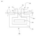
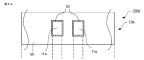
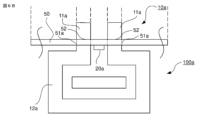
- 6A and 6B are a plan view (upper side) and a front view (lower side), respectively, showing one current sensor 30a constituting a main part of a power conversion device 100a according to the second embodiment.
- the shield portion 11a which is the two legs of the convex core 10a constituting the gap portion 13a, is inserted into two through holes 51a provided in the substrate 50, and adhesive 52 is applied to the boundary portion (the gap) between the two legs of the convex core 10a and the through hole 51a.
- the adhesive 52 is used to fix the shield portion 11a, which is the two legs of the convex core 10a, to the two through holes 51a provided in the substrate 50, thereby reducing the relative displacement between the gap portion 13a and the predetermined position of the magnetoelectric conversion element 20a caused by external forces such as vibration. This improves the accuracy of current detection in the power conversion device 100a.
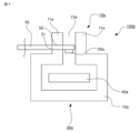
- FIG. 7 is a front view showing one current sensor 30a which is a main part of a power conversion device 100b according to the third embodiment.
- the power conversion device 100b according to the third embodiment differs from the power conversion devices shown in the first and second embodiments in that one of the two legs of the convex core 10a is inserted into one through hole 51a provided in the substrate 50 and is arranged on the substrate 50.
- the left shield part (hereinafter also referred to as the left leg) is inserted into the through hole 51 and disposed on the substrate 50.
- the left leg part of the convex core 10a and the through hole 51 can maintain the relative positional relationship between the position of the gap part 13a and the position of the magneto-electric conversion element 20a against the external force such as vibration, so that the accuracy of current detection of the power conversion device 100 can be improved compared to the case where it is affected by an external force such as vibration.
- the shield portion 11a is disposed in the vicinity of the magnetoelectric conversion element 20a, the influence of an external magnetic field on the magnetoelectric conversion element 20a due to a change in the position of the gap portion 13a can be reduced.
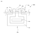
- Embodiment 4 A power conversion device 100c according to the fourth embodiment will be described below with reference to the drawings. 8 is a front view showing one current sensor 30a which is a main part of a power conversion device 100c according to embodiment 4.
- the power conversion device 100c according to embodiment 4 differs from the configurations shown in embodiments 1 and 2 in that the magnetoelectric conversion element is disposed on the upper surface of the substrate 50 on the side farther from the bus bar.
- the gap portion 13a of the convex core 10a is configured to penetrate the substrate 50 on which the magnetoelectric conversion element is arranged, so that the magnetoelectric conversion element 20b can be arranged on either the upper or lower surface of the substrate 50.
- the temperature of the bus bar 40a rises.
- the magnetic field detection accuracy of the magnetoelectric conversion element 20b changes due to the influence of temperature changes, so the influence of temperature changes from the bus bar 40a can be reduced when the magnetoelectric conversion element 20b is arranged on the surface of the substrate 50 farther from the bus bar 40a than when it is arranged on the surface closer to the bus bar 40a.
- the magnetoelectric conversion element 20a is arranged on the surface of the substrate 50 farther from the busbar 40a, as in the power conversion device 100c of the fourth embodiment, the effect of temperature changes from the busbar 40a can be reduced, improving the detection accuracy of the current flowing through the busbar 40a.
- Embodiment 5 A power conversion device 100d according to the fifth embodiment will be described below with reference to the drawings. 9 is a front view showing one current sensor 30a which is a main part of a power conversion device 100d according to embodiment 5.
- the power conversion device 100d according to embodiment 5 differs from the configurations shown in embodiments 1 and 2 in that two magnetoelectric conversion elements 20a, 20b are arranged on both sides of a substrate 50.
- the gap portion 13a of the convex core 10a is inserted into the through hole 51a of the substrate 50, so that the magnetoelectric conversion elements 20a and 20b can be arranged on both sides of the substrate 50.
- the magnetoelectric conversion elements 20a and 20b By arranging the magnetoelectric conversion elements 20a and 20b on the bottom and top surfaces of the substrate 50, respectively, it is possible to provide redundancy to the current detection function of the current sensor 30a.
- the magnetoelectric conversion element 20a arranged on one side of the substrate 50 is the main element and the magnetoelectric conversion element 20b arranged on the other side is the sub element, during normal operation the value obtained from the magnetoelectric conversion element 20a is acquired as the current detection value. If the magnetoelectric conversion element 20a is shorted to the power or ground, or if another fault occurs, it can be determined whether or not a fault has occurred in the magnetoelectric conversion element 20a by comparing the value with that of the sub magnetoelectric conversion element 20b arranged on the other side of the substrate 50. Note that the division of roles between the main and sub magnetoelectric conversion elements described above means that either the magnetoelectric conversion element 20a or 20b can be designated as the main element.
- the various features, aspects, and functions described in one or more embodiments are not limited to application to a particular embodiment, but may be applied to the embodiments alone or in various combinations. Therefore, countless modifications not exemplified are assumed within the scope of the technology disclosed in the present specification, including, for example, modifying, adding, or omitting at least one component, and further, extracting at least one component and combining it with a component of another embodiment.
- the power conversion devices according to the first to fifth embodiments can be mounted and used in various electric vehicles, for example, hybrid vehicles or electric vehicles (EVs).
- the control speed is increased in order to improve the output accuracy.
- the faster the control speed the higher the noise level tends to be. Therefore, the present power conversion device, which can improve the current detection accuracy by reducing the influence of the external magnetic field, is particularly useful.
Landscapes
- Engineering & Computer Science (AREA)
- Power Engineering (AREA)
- Measuring Instrument Details And Bridges, And Automatic Balancing Devices (AREA)
Abstract
電力変換装置(100)において、貫通孔(51a、51b、51c)を有する基板(50)と、パワーモジュールに接続され基板(50)と対向して配置されたバスバー(40a、40b、40c)と、バスバー(40a、40b、40c)を取り囲み、切欠きを有する筒体であって、切欠きに沿って形成された1対の突出部(11a、11b、11c)を有するコア(10a、10b、10c)と、基板(50)に配置された磁電変換素子(20a、20b、20c)と、を備え、コア(10a、10b、10c)の1対の突出部(11a、11b、11c)のうち少なくとも1つは、貫通孔(51a、51b、51c)に挿入されて基板(50)に固定され、磁電変換素子(20a、20b、20c)は、コア(10a、10b、10c)の切欠き部分、またはコア(10a、10b、10c)の1対の突出部(11a、11b、11c)の間隙に配置するようにした。
Description
本願は電力変換装置および電動車両に関するものである。
電気自動車またはハイブリッド自動車の様に、駆動源にモータが用いられている電動車両には、複数の電力変換装置が搭載されている。電力変換装置は、モータの駆動または駆動エネルギーのバッテリへの回生などに用いられる。具体的な電力変換装置としては、商用の交流電源から直流電源に変換して高圧バッテリに充電する充電器、高圧バッテリの直流電源から補助機器用のバッテリの電圧(例えば12V)に変換するDC/DCコンバータ、バッテリから直流電力をモータへの交流電力に変換するインバータなどが挙げられる。
電力変換装置の内部には、大電流をスイッチングする素子及び電力変換機能を制御する演算回路に加えて、バスバーに流れる電流を測定する電流センサなどが設けられる。このように電力変換装置の内部には多くの電気部品が含まれるため、電力変換装置のサイズが大きくなるという課題があった。
電力変換装置の大型化を抑制するために、電流センサを他の部品と一体的に形成した構成が開示されている(例えば、特許文献1参照)。電流センサは、バスバーと、磁性体からなるC字状のコアと、磁電変換素子で構成されており、バスバーはC字状のコアの内側に配置され、磁電変換素子はC字状のコアのギャップ部に設けられている。
上記C字状のコアは切欠き部のギャップ長を短く形成できるため、磁電変換素子への集磁効果を高めることができる。そのため、電流センサを構成する磁性体コアにC字状のコアがよく用いられる。磁電変換素子は基板に接続され、バスバーを流れる電流に起因して切り欠き部に生じた磁束を検知する。コアは、磁電変換素子に対する外部からの磁界影響を低減させるためのシールド部を備える。
上記特許文献1においては、C字状のコアの側面部をC字状のコアの底部と対向に延出させて電流センサとシールド部が一体的に形成されているため、C字状のコアによる高い集磁効果を維持しつつ、磁電変換素子に対する外部からの磁界影響を低減し、電力変換装置を小型化することができる。
しかしながら、振動などの外力により基板上に設けられる磁電変換素子がコアのギャップ部の所定位置から位置ズレすることで、電力変換装置の電流検出精度が低下するという課題があった。また、電力変換装置の小型化に伴い、電気部品ごとの相対距離が小さくなり、コアのギャップ部に対する外部からの磁界影響が大きくなることから、外部の磁界影響を低減するためにはシールド部が大きくなる課題があった。
そこで、本願は、コアによる高い集磁効果および電力変換装置の小型化を維持しつつ、コアのギャップ部に対する磁電変換素子の位置決め精度を向上させ電流検出精度が向上できるとともに、コアのギャップ部に対する外部からの磁界影響を低減させることができる電力変換装置を得ることを目的としている。
本願に開示される電力変換装置は、
貫通孔を有する基板と、
パワーモジュールに接続され、前記基板と対向するように配置されたバスバーと、
前記バスバーを取り囲み、切欠きを有する筒体であって、前記切欠きに沿って形成された1対の突出部を有するコアと、
前記基板に配置され、検知した磁界を電気信号に変換する磁電変換素子と、
を備え、
前記コアの1対の突出部のうち少なくとも1つは、前記貫通孔に挿入されて前記基板に固定されているとともに、
前記磁電変換素子は、前記コアの切欠き部分、または前記コアの1対の突出部の間隙に配置されている、
ことを特徴とするものである。
貫通孔を有する基板と、
パワーモジュールに接続され、前記基板と対向するように配置されたバスバーと、
前記バスバーを取り囲み、切欠きを有する筒体であって、前記切欠きに沿って形成された1対の突出部を有するコアと、
前記基板に配置され、検知した磁界を電気信号に変換する磁電変換素子と、
を備え、
前記コアの1対の突出部のうち少なくとも1つは、前記貫通孔に挿入されて前記基板に固定されているとともに、
前記磁電変換素子は、前記コアの切欠き部分、または前記コアの1対の突出部の間隙に配置されている、
ことを特徴とするものである。
本願に開示される電力変換装置によれば、磁性体からなるコアの突出部が基板に設けられた1つ以上の貫通孔に挿入され、磁電変換素子が貫通孔近傍の基板の部分に配置されているため、コアによる高い集磁効果を維持しつつ、基板に対して位置決めの役割も兼ねている。よって、コアのギャップ部に対する磁電変換素子の位置決め精度を向上させ電流検出精度が向上できるとともに、コアのギャップ部に対する外部からの磁界影響を低減させることができる電力変換装置を得ることができる。
以下、本願の実施の形態による電力変換装置を図に基づいて説明する。なお、各図において同一、または相当部材、部位については同一符号を付して説明する。
実施の形態1.
電力の変換を行う電力変換装置100は、モータを駆動源の一つとする電気自動車、もしくはハイブリット自動車等の車両に搭載されて用いられる。この電力変換装置100について、以下図1を用いてその構成の概要をまず説明する。
電力の変換を行う電力変換装置100は、モータを駆動源の一つとする電気自動車、もしくはハイブリット自動車等の車両に搭載されて用いられる。この電力変換装置100について、以下図1を用いてその構成の概要をまず説明する。
図1は上記電力変換装置100の概略の構成を示す模式図である。この図1は、また、前記電力変換装置100について、主要な構成部品である基板50の下面側から見た場合の図でもある。
図1に示すように、バスバー40a、40b、40cは、それぞれ、上記基板50に取り付けられた電流センサ30a、30b、30c(この電流センサについては、以下で詳しく説明する)を構成する、上部に切欠きを有し正面から見た場合の形状が凸字状のコア10a、10b、10cの内側を貫通するように構成されており(バスバー、凸字状のコアについても以下で詳しく説明する)、電力変換装置100が備えるパワーモジュール70a、70b、70cとそれぞれ接続される。
なお、以上においては、パワーモジュール70a、70b、70cは、別々のものを前提として説明したが、これらは一体化したものでも構わない。そこで、次に、上記電力変換装置100の要部の構成について、以下図2~図5を用いて詳しく説明する。
図2は実施の形態1に係る電力変換装置100の要部を示す斜視図、図3は電力変換装置100の要部を示す正面図である。ここで、図2及び図3は、電力変換装置100の全体の構成から電力変換装置100を取り囲む筐体を取り除いた場合の図となっている。また、図4は図2の電力変換装置100の要部である電流センサ30aを示す正面図、図5は図4の電流センサ30aの要部である凸字状のコア10aを示す正面図である。
<電力変換装置の構成>
電力変換装置100は、図2及び図3に示したように、3相の電流の各相がそれぞれに流れる3本の平板状のバスバー40a、40b、40cを備える。そして、3相の電流のそれぞれの電流値を測定するために、バスバー40aには電流センサ30a、バスバー40bには電流センサ30b、バスバー40cには電流センサ30cが、それぞれ設けられている。
なお、上記バスバー40a、40b、および40cは同様の形状を有している。また、上記電流センサ30a、30b、および30cは以下に説明するように、同様の構成を有している。
電力変換装置100は、図2及び図3に示したように、3相の電流の各相がそれぞれに流れる3本の平板状のバスバー40a、40b、40cを備える。そして、3相の電流のそれぞれの電流値を測定するために、バスバー40aには電流センサ30a、バスバー40bには電流センサ30b、バスバー40cには電流センサ30cが、それぞれ設けられている。
なお、上記バスバー40a、40b、および40cは同様の形状を有している。また、上記電流センサ30a、30b、および30cは以下に説明するように、同様の構成を有している。
また、電力変換装置100は、上述のバスバー40a、40b、40cの他、電流センサ30a、30b、30cを構成する凸字状のコア、10a、10b、10c、及び基板50の表面に搭載された磁電変換素子20a、20b、20cを備える。
ここで上記各コアは、全体として筒体であって、切欠きを有し、当該切欠きに沿って1対の柱状体(以降、1対の突出部とも呼ぶ)が外側に向けて対向して配置されている。
ここで上記各コアは、全体として筒体であって、切欠きを有し、当該切欠きに沿って1対の柱状体(以降、1対の突出部とも呼ぶ)が外側に向けて対向して配置されている。
ここで、上記3本のバスバー40a、40b、40cは、それぞれ、u相、v相、w相の3相の電流の各相が流れる導体である。これら3本のバスバーは、例えば、銅もしくはアルミニウムで作製される。ただし、材料はこれらに限るものではなく、電流が流れる材料であれば他の材料でも構わない。
また、装置の正面から見た場合に凸字状に形成されたコア10a、10b、10cは、図2及び図3に示したように、それぞれ、磁性体からなり、装置の正面から見た場合にC字状を形成したコア12a、12b、12cと、このC字状のコアの端部をバスバー40a、40b、40cの設置された位置とは反対方向に延出させた1対の突出部11a、11b、11c(以下では、シールド部とも呼ぶ)を備えている。
なお、基板50には、上述した磁電変換素子20a、20b、20cに加え、IC(Integrated Circuit)、抵抗、コンデンサ等の受動部品、及び他の必要な電気部品、例えば、前記パワーモジュールの動作を制御する回路が実装される。基板50は、バスバー40a、40b、40cのそれぞれに流れる電流を、磁電変換素子20a、20b、20cにより検出する機能を備える。
また、磁電変換素子20a、20b、20cは、測定対象のバスバー40a、40b、40cにそれぞれ流れる電流に起因して生じた磁界以外の磁界である外部磁界も検出する。磁電変換素子20a、20b、および20cが検出したこの外部磁界は、電流測定の誤差となる。
例えば、測定対象がバスバー40aである場合、隣接するバスバー40b、40cに流れる電流に起因して発生した磁界は外部磁界の1つとなる。精度よく電流を測定するためには、外部磁界の影響を抑制することが重要である。そのため、磁電変換素子20aの感磁部分を一対の突出部11aの内側に構成された隙間13a(以下、ギャップ部13aとも呼ぶ)の所定の位置に配置することが望ましい。なお、隙間13b(以下、ギャップ部13bとも呼ぶ)、および隙間13c(以下、ギャップ部13cとも呼ぶ)についても同様である。
ここで、バスバー40aに流れる電流に起因して生じた磁界を凸字状のコア10aが集磁した場合の集磁の効率は、ギャップ部13aのギャップのサイズに反比例する。ギャップ部13aのサイズを縮めることで、コアで生ずる集磁の効率を向上させることができ、突出部11aが磁電変換素子20aのより近傍に配置されることで、外部磁界の影響を受けにくくなる。
なお、本実施の形態1の電力変換装置100には、表面実装型の磁電変換素子を用いることができる。この場合、磁電変換素子は、基板50に表面実装される。なお、磁電変換素子の基板50への取付け形態は表面実装型に限るものではないが、表面実装型の磁電変換素子を用いることで、磁電変換素子に対する振動の影響が抑制され、ひいては、電力変換装置100の電流検出の精度を向上させることができる。
また、本実施の形態1では、図3に点線の枠で囲んで示したように、凸字状のコア10a、10b、10cのそれぞれ一部とバスバー40a、40b、40cは、樹脂60により一体化されている。
複数の凸字状のコア10a、10b、10cと複数のバスバー40a、40b、40cとを樹脂成型などで一体化した場合、複数の部品を1つの部品として扱うことができる。
このように、複数の部品を1つの部品として扱うことができるため、組み立て及び検査工程を省力化することができ、電力変換装置100の生産性を向上させることができる。
このように、複数の部品を1つの部品として扱うことができるため、組み立て及び検査工程を省力化することができ、電力変換装置100の生産性を向上させることができる。
なお、凸字状のコア10a、10b、10cとバスバー40a、40b、40cとがそれぞれ分かれて組み合わされ、樹脂60により、それぞれ別々の組み合わせ(例えば、凸字状のコア10aとバスバー40aの組み合わせで一体化)で一体化されても構わない。
また、本実施の形態1では、図2に示したように、電流センサ30a、30b、30cを基板50の端(手前側に寄せる形態)に並べて配置したが、電流センサ30a、30b、30cの配置は、これに限るものではない。また、基板50に貫通孔51a、51b、51cが形成されている場合には、凸字状のコア10a等は、基板50の端ではなく、中央にも配置することが可能である。
従って、電力変換装置100においては、基板50に搭載する電気部品及び電流センサ30a、30b、30cの配置の自由度は向上し、電力変換装置100の生産性を向上させることができる。
以上において、上記電流センサ30aは、凸字状のコア10aと磁電変換素子20aから構成され、上記電流センサ30bは、凸字状のコア10bと磁電変換素子20bから構成され、上記電流センサ30cは、凸字状のコア10cと磁電変換素子20cから構成される。
以上、実施の形態1の電力変換装置においては、ギャップ部13a、13b、13cに対する各磁電変換素子20a、20b、20cの組付け誤差を低減できる。具体的には、上記コアの一対の突出部を基板の貫通孔に固定することにより、凸字状のコアと基板とを一体型に構成したため、寸法公差などの誤差要因が小さくできる。
以上、実施の形態1の電力変換装置においては、ギャップ部13a、13b、13cに対する各磁電変換素子20a、20b、20cの組付け誤差を低減できる。具体的には、上記コアの一対の突出部を基板の貫通孔に固定することにより、凸字状のコアと基板とを一体型に構成したため、寸法公差などの誤差要因が小さくできる。
なお、凸字状のコア10a、10b、および10cは、いずれも同様の形状を有しており、各々、その一部が基板50を貫通して取付けられている。また、磁電変換素子20a、20b、および20cは、いずれも同様の形状を有しており、基板50の面上に同様に配置されている。
そこで、以下では、上記電流センサ30aを代表として取り上げ、その構成について、上記電力変換装置を正面からみた正面図である図4および図5を用いてさらに詳しく説明する。
そこで、以下では、上記電流センサ30aを代表として取り上げ、その構成について、上記電力変換装置を正面からみた正面図である図4および図5を用いてさらに詳しく説明する。
<電流センサ>
電流センサ30aは、図4に示すように、凸字状のコア10a、磁電変換素子20a、及びバスバー40aから構成される。この凸字状のコア10aは上述したように、C字状のコア12aと突出部11aとから形成されているが、図4に示したように、C字状のコア12aの端部と突出部11aが、左右対称的に一つずつ対向して一対で形成されているため、隙間13a(ギャップ部13a)が形成される。そして、上記磁電変換素子20aは、このギャップ部13a内で、基板50の面上に配置されている。なお、図4、図5では、電力変換装置は平面的な図であるため、これらの図においては、コア10aを凸字状のコア10aと呼ぶ(以下同様)。なお、以上では、図4との関係で、図2、図3に示したコア10b、10cにそれぞれ関わるC字状のコア12b、12cについては説明しなかったが、これらについても、C字状のコア12aの場合と同様である。
電流センサ30aは、図4に示すように、凸字状のコア10a、磁電変換素子20a、及びバスバー40aから構成される。この凸字状のコア10aは上述したように、C字状のコア12aと突出部11aとから形成されているが、図4に示したように、C字状のコア12aの端部と突出部11aが、左右対称的に一つずつ対向して一対で形成されているため、隙間13a(ギャップ部13a)が形成される。そして、上記磁電変換素子20aは、このギャップ部13a内で、基板50の面上に配置されている。なお、図4、図5では、電力変換装置は平面的な図であるため、これらの図においては、コア10aを凸字状のコア10aと呼ぶ(以下同様)。なお、以上では、図4との関係で、図2、図3に示したコア10b、10cにそれぞれ関わるC字状のコア12b、12cについては説明しなかったが、これらについても、C字状のコア12aの場合と同様である。
ここで、基板50は、磁電変換素子20aの左右に、2つの貫通孔51aを有するため、すなわち、磁電変換素子20aは、2つの貫通孔51aの間の基板50の面上に配置され、検知した磁界を電気信号に変換して出力する。ただし、図4では、磁電変換素子20aは、基板50の表面、裏面の両方の面ではなく、バスバー40aと対向する基板50の一方の面にだけ配置されている。
具体的には、磁電変換素子20aを基板50の一方の面に配置する場合、磁電変換素子20aはバスバー40aに近い側の基板50の面(図4では下面)に配置することで、磁電変換素子20aは、外部磁界の影響を受けにくくなる。従って、ノイズとなる外部磁界の影響が小さくなり、SN比(信号/ノイズの比)を大きくすることができるため、電力変換装置100の電流検出の精度を向上させることができる。
ここで、上記磁電変換素子20aには、例えばホール素子もしくはMR(Magneto Resistive)素子が用いられる。MR素子には、AMR(Anisotropic Magneto Resistive、異方性磁気抵抗)素子、GMR(Giant Magneto Resistive、巨大磁気抵抗)素子、TMR(Tunnel Magneto Resistive、トンネル型磁気抵抗)素子などがあるが、何れの素子であっても構わない。なお、磁電変換素子20aはこれらの素子に限るものではなく、検知した磁界を電気信号に変換して出力する機能を備えていれば他の素子でも構わない。
なお、磁電変換素子20aの実装場所は基板50の一方の面に限るものではなく、基板50の他方の面に実装しても構わない。凸字状のコア10aのギャップ部13aに磁電変換素子20aが配置されていれば、バスバー40aに流れた電流に起因した磁束を検知することができるためである。
一方、図5に示したように、上記凸字状のコア10aは、磁性体からなるC字状のコア12aと突出部11a(シールド機能を有するためシールド部11aとも言う。図5でハッチングを施した部分を参照)から一体的に形成され、凸字状のコア10aを貫通してバスバー40aが設置されている。
この場合においては、図4に示したように、凸字状のコア10aの脚部である1対の突出部11aが、図4で左右に位置する2つの貫通孔51aのそれぞれに挿入されて、基板50に配置されている。つまり、電流センサ30aの構成部品である凸字状のコア10aは、基板50と一体的に設けられており、この凸字状のコア10aと基板50の双方のスペースが共有されているため、電力変換装置100においては、基板50の表面に垂直な方向において、貫通孔51aのない基板と比較して、低背化することができる。
また、凸字状のコア10aの脚部である突出部11aを貫通孔51に挿入しているため、振動等の外力による磁電変換素子20aの鉛直方向の変位に対して、ギャップ部13aと磁電変換素子20aの相対的な位置関係が変化した状態となることなく、相対的な位置関係を維持することができる。
また、磁電変換素子20aの近傍にシールド部11aが配置されるため、ギャップ部13aに対する外部からの磁界の影響を低減することができる。このことから、電力変換装置100の電流検出精度を向上することができることがわかる。
なお、凸字状のコア10aの材料は、例えば電磁鋼板、鉄、パーマロイ、もしくはフェライトが用いられる。これらの材料は、鉄、ニッケル、コバルトといった強磁性材料、もしくは強磁性体材料を含有した材料であればよく、特に軟磁性材料が適している。凸字状のコア10aの製方法は、巻き鉄心でも積層でも構わない。
ここで、バスバー40aに流れた電流に起因して、上記ギャップ部13aに生じた磁界が、磁電変換素子20aに到達する。磁電変換素子20aの感磁(磁力線ベクトル)の主方向は、磁電変換素子20aが配置された基板50の配置面に平行な方向である。そして、磁電変換素子20aは感磁した磁界の大きさに応じた電圧を発生させ、発生した電圧を電流に変換し、測定された電流の大きさに相当する電気信号を基板50に設けられた回路に出力する。
なお、ここでは磁電変換素子20aの有するICが、磁界を電流に変換して、磁界の大きさを電流の値に換算する換算器を備えた構成を仮定して説明するが、磁電変換素子20aとは異なる別体のICが上記換算器を備え、基板50にこの別体のICが搭載されていても構わない。
実施の形態2.
実施の形態2に係る電力変換装置100aについて、以下図を用いて説明する。
図6A、図6Bは、それぞれ実施の形態2に係る電力変換装置100aの要部を構成する一つの電流センサ30aを示す平面図(上側)及び正面図(下側)である。
実施の形態2に係る電力変換装置100aについて、以下図を用いて説明する。
図6A、図6Bは、それぞれ実施の形態2に係る電力変換装置100aの要部を構成する一つの電流センサ30aを示す平面図(上側)及び正面図(下側)である。
本実施の形態2に係る電力変換装置100aは、実施の形態1に示した構成に加えて、ギャップ部13aを構成する凸字状のコア10aの2つの脚部であるシールド部11aが基板50に設けられた2つの貫通孔51aに挿入され、凸字状のコア10aの2つの脚部と貫通孔51aの境界部分(の隙間)には接着剤52が施されている。
図6Aにおいて、接着剤52により、凸字状のコア10aの2つの脚部であるシールド部11aと基板50に設けられる2つの貫通孔51aとが固定されているため、振動等の外力によるギャップ部13aと磁電変換素子20aの所定位置との相対的な変位量を低減できる。よって、電力変換装置100aの電流検出の精度を向上させることができる。
実施の形態3.
実施の形態3に係る電力変換装置100bについて、以下図を用いて説明する。
図7は実施の形態3に係る電力変換装置100bの要部である一つの電流センサ30aを示す正面図である。
実施の形態3に係る電力変換装置100bについて、以下図を用いて説明する。
図7は実施の形態3に係る電力変換装置100bの要部である一つの電流センサ30aを示す正面図である。
本実施の形態3に係る電力変換装置100bは、実施の形態1と実施の形態2に示した電力変換装置の構成とは異なり、凸字状のコア10aの2つの脚部の何れか一方が、基板50に設けられた1つの貫通孔51aに挿入され、基板50に配置された構成になっている。
具体的には、図7において、凸字状のコア10aの2つのシールド部11aのうち、左に位置するシールド部(以下、左の脚部とも呼ぶ)が、貫通孔51に挿入されて基板50に配置されている。凸字状のコア10aの左脚部と貫通孔51により、振動等の外力が発生した場合でも、振動等の外力に対して、ギャップ部13aの位置と磁電変換素子20aの位置との相対的な位置関係を保持することができるため、電力変換装置100の電流検出の精度を、振動等の外力による影響がある場合に比べて、向上させることができる。
また、磁電変換素子20aの近傍に、シールド部11aが配置されるため、ギャップ部13aの位置変化による磁電変換素子20aに対する外部からの磁界の影響を低減することができる。
また、磁電変換素子20aの近傍に、シールド部11aが配置されるため、ギャップ部13aの位置変化による磁電変換素子20aに対する外部からの磁界の影響を低減することができる。
実施の形態4.
実施の形態4に係る電力変換装置100cについて、以下図を用いて説明する。
図8は実施の形態4に係る電力変換装置100cの要部である一つの電流センサ30aを示す正面図である。本実施の形態4に係る電力変換装置100cでは、実施の形態1と実施の形態2に示した構成に比べて、磁電変換素子が、バスバーから遠い側の基板50の上面に配置された構成になっている点が異なる。
実施の形態4に係る電力変換装置100cについて、以下図を用いて説明する。
図8は実施の形態4に係る電力変換装置100cの要部である一つの電流センサ30aを示す正面図である。本実施の形態4に係る電力変換装置100cでは、実施の形態1と実施の形態2に示した構成に比べて、磁電変換素子が、バスバーから遠い側の基板50の上面に配置された構成になっている点が異なる。
図8において、凸字状のコア10aのギャップ部13aは、磁電変換素子が配置される基板50を貫通するように構成されているため、磁電変換素子20bは基板50の上面あるいは下面の何れの面にも配置できる。バスバー40aに電流が通電された場合、バスバー40aの温度が上昇する。この場合において、磁電変換素子20bは、温度変化の影響により、磁界検出精度が変化するため、基板50のバスバー40aに近い側の面に配置された場合よりも、バスバー40aから遠い側の面に配置された場合の方が、バスバー40aからの温度変化の影響を低減できる。
ギャップ部13aに磁電変換素子20b以外の電子部品もしくはパターンがあると、それらが磁界を発生させるため、ギャップ部13aを含めた集磁経路にあるバスバー40aからの磁束を妨げる働きをするため、バスバー40aに流れる電流の検出精度が低下する。よって、ギャップ部13aには、可能な限りにおいて磁電変換素子20b以外の電子部品を配置しないようにする。
本実施の形態4の電力変換装置100cのように、磁電変換素子20aを基板50のバスバー40aから遠い側の面に磁電変換素子20bを配置した場合、バスバー40aからの温度変化の影響を低減できるため、バスバー40aに流れる電流の検出精度を向上できる。
実施の形態5.
実施の形態5に係る電力変換装置100dについて、以下図を用いて説明する。
図9は実施の形態5に係る電力変換装置100dの要部である一つの電流センサ30aを示す正面図である。実施の形態5に係る電力変換装置100dは、実施の形態1と実施の形態2に示した構成に比べて、2つの磁電変換素子20a、20bが基板50の両面に配置された構成になっている点が異なる。
実施の形態5に係る電力変換装置100dについて、以下図を用いて説明する。
図9は実施の形態5に係る電力変換装置100dの要部である一つの電流センサ30aを示す正面図である。実施の形態5に係る電力変換装置100dは、実施の形態1と実施の形態2に示した構成に比べて、2つの磁電変換素子20a、20bが基板50の両面に配置された構成になっている点が異なる。
図9において、凸字状のコア10aのギャップ部13aは、基板50の貫通孔51aに挿入されているため、基板50の両面に磁電変換素子20a、20bを配置できる。磁電変換素子20a、および磁電変換素子20bをそれぞれ、基板50の下面および上面に配置することで、電流センサ30aの電流検出機能に冗長性を持たせることができる。
例えば、基板50の一方の面に配置される磁電変換素子20aがメインとして、もう一方の面に配置される磁電変換素子20bがサブとなった場合、通常動作時は、磁電変換素子20aから得られる値を電流検出値として取得する。磁電変換素子20aが天絡、または地絡、あるいは他の障害が生じた場合、基板50のもう一方の面に配置されたサブの磁電変換素子20bの値と比較することで、磁電変換素子20aに故障が生じているか否かを判断することができる。なお、上記磁電変換素子のメインとサブの役割分担は、磁電変換素子20aと20bのどちらをメインとしても構わない。
また本願は、様々な例示的な実施の形態及び実施例が記載されているが、1つ、または複数の実施の形態に記載された様々な特徴、態様、及び機能は特定の実施の形態の適用に限られるのではなく、単独で、または様々な組み合わせで実施の形態に適用可能である。
従って、例示されていない無数の変形例が、本願明細書に開示される技術の範囲内において想定される。例えば、少なくとも1つの構成要素を変形する場合、追加する場合または省略する場合、さらには、少なくとも1つの構成要素を抽出し、他の実施の形態の構成要素と組み合わせる場合が含まれるものとする。
具体的には、上記実施の形態1から5に係る電力変換装置は、種々の電動車両、例えば、ハイブリッド車両、あるいは電気自動車(EV)に搭載して使用することができる。この場合において、電動車両に搭載される電力変換装置では、出力精度の向上のため、制御が高速化している。しかし、制御が高速になるほど、ノイズレベルが増大する傾向にある。よって、外部磁界の影響を低減することで、電流検出精度を向上できる本電力変換装置が特に有用となる。
従って、例示されていない無数の変形例が、本願明細書に開示される技術の範囲内において想定される。例えば、少なくとも1つの構成要素を変形する場合、追加する場合または省略する場合、さらには、少なくとも1つの構成要素を抽出し、他の実施の形態の構成要素と組み合わせる場合が含まれるものとする。
具体的には、上記実施の形態1から5に係る電力変換装置は、種々の電動車両、例えば、ハイブリッド車両、あるいは電気自動車(EV)に搭載して使用することができる。この場合において、電動車両に搭載される電力変換装置では、出力精度の向上のため、制御が高速化している。しかし、制御が高速になるほど、ノイズレベルが増大する傾向にある。よって、外部磁界の影響を低減することで、電流検出精度を向上できる本電力変換装置が特に有用となる。
10a、10b、10c コア、11a、11b、11c 突出部(シールド部)、12a、12b、12c C字状のコア、13a、13b、13c ギャップ部(隙間)、20a、20b、20c 磁電変換素子、30a、30b、30c 電流センサ、40a、40b、40c バスバー、50 基板、51、51a、51b、51c 貫通孔、52 接着剤、60 樹脂、70a、70b、70c パワーモジュール、100、100a、100b、100c、100d 電力変換装置
Claims (7)
- 貫通孔を有する基板と、
パワーモジュールに接続され、前記基板と対向するように配置されたバスバーと、
前記バスバーを取り囲み、切欠きを有する筒体であって、前記切欠きに沿って形成された1対の突出部を有するコアと、
前記基板に配置され、検知した磁界を電気信号に変換する磁電変換素子と、
を備え、
前記コアの1対の突出部のうち少なくとも1つは、前記貫通孔に挿入されて前記基板に固定されているとともに、
前記磁電変換素子は、前記コアの切欠き部分、または前記コアの1対の突出部の間隙に配置されている、
ことを特徴とする電力変換装置。 - 前記突出部と前記貫通孔とが接着剤で固定されていることを特徴とする請求項1に記載の電力変換装置。
- 前記コアと前記バスバーとが樹脂で一体化されていることを特徴とする請求項1または2に記載の電力変換装置。
- 前記磁電変換素子は、前記バスバーと対向する前記基板の少なくとも一方の面上に配置されていることを特徴とする請求項1または2に記載の電力変換装置。
- 前記磁電変換素子は、前記基板に表面実装されていることを特徴とする請求項1または2に記載の電力変換装置。
- 前記基板は、前記パワーモジュールの動作を制御する回路を有することを特徴とする請求項1から5のいずれか1項に記載の電力変換装置。
- 請求項1から6のいずれか1項に記載の電力変換装置を備えたことを特徴とする電動車両。
Priority Applications (4)
| Application Number | Priority Date | Filing Date | Title |
|---|---|---|---|
| CN202380098801.3A CN121263950A (zh) | 2023-06-06 | 2023-06-06 | 功率转换装置和电动车辆 |
| JP2025525483A JPWO2024252509A1 (ja) | 2023-06-06 | 2023-06-06 | |
| PCT/JP2023/020929 WO2024252509A1 (ja) | 2023-06-06 | 2023-06-06 | 電力変換装置および電動車両 |
| DE112023006465.2T DE112023006465T5 (de) | 2023-06-06 | 2023-06-06 | Leistungsumwandlungsvorrichtung und elektrofahrzeug |
Applications Claiming Priority (1)
| Application Number | Priority Date | Filing Date | Title |
|---|---|---|---|
| PCT/JP2023/020929 WO2024252509A1 (ja) | 2023-06-06 | 2023-06-06 | 電力変換装置および電動車両 |
Publications (1)
| Publication Number | Publication Date |
|---|---|
| WO2024252509A1 true WO2024252509A1 (ja) | 2024-12-12 |
Family
ID=93795319
Family Applications (1)
| Application Number | Title | Priority Date | Filing Date |
|---|---|---|---|
| PCT/JP2023/020929 Ceased WO2024252509A1 (ja) | 2023-06-06 | 2023-06-06 | 電力変換装置および電動車両 |
Country Status (4)
| Country | Link |
|---|---|
| JP (1) | JPWO2024252509A1 (ja) |
| CN (1) | CN121263950A (ja) |
| DE (1) | DE112023006465T5 (ja) |
| WO (1) | WO2024252509A1 (ja) |
Citations (6)
| Publication number | Priority date | Publication date | Assignee | Title |
|---|---|---|---|---|
| JP2011242276A (ja) * | 2010-05-19 | 2011-12-01 | Auto Network Gijutsu Kenkyusho:Kk | 電流センサ |
| JP2012247420A (ja) * | 2011-05-30 | 2012-12-13 | Melexis Technologies Nv | 電線を流れる電流を測定するための装置 |
| JP2014106101A (ja) * | 2012-11-27 | 2014-06-09 | Toyota Industries Corp | 電流センサ |
| JP2021175248A (ja) * | 2020-04-23 | 2021-11-01 | 三菱電機株式会社 | 電力変換装置 |
| JP2022519060A (ja) * | 2019-01-30 | 2022-03-18 | レム・インターナショナル・エスエイ | 磁界検出器モジュールを備えた電流変換器 |
| WO2023090228A1 (ja) * | 2021-11-16 | 2023-05-25 | 株式会社デンソー | 電流センサ |
Family Cites Families (1)
| Publication number | Priority date | Publication date | Assignee | Title |
|---|---|---|---|---|
| JP6372969B2 (ja) | 2012-12-03 | 2018-08-15 | 矢崎総業株式会社 | 電流センサ |
-
2023
- 2023-06-06 CN CN202380098801.3A patent/CN121263950A/zh active Pending
- 2023-06-06 JP JP2025525483A patent/JPWO2024252509A1/ja active Pending
- 2023-06-06 WO PCT/JP2023/020929 patent/WO2024252509A1/ja not_active Ceased
- 2023-06-06 DE DE112023006465.2T patent/DE112023006465T5/de active Pending
Patent Citations (6)
| Publication number | Priority date | Publication date | Assignee | Title |
|---|---|---|---|---|
| JP2011242276A (ja) * | 2010-05-19 | 2011-12-01 | Auto Network Gijutsu Kenkyusho:Kk | 電流センサ |
| JP2012247420A (ja) * | 2011-05-30 | 2012-12-13 | Melexis Technologies Nv | 電線を流れる電流を測定するための装置 |
| JP2014106101A (ja) * | 2012-11-27 | 2014-06-09 | Toyota Industries Corp | 電流センサ |
| JP2022519060A (ja) * | 2019-01-30 | 2022-03-18 | レム・インターナショナル・エスエイ | 磁界検出器モジュールを備えた電流変換器 |
| JP2021175248A (ja) * | 2020-04-23 | 2021-11-01 | 三菱電機株式会社 | 電力変換装置 |
| WO2023090228A1 (ja) * | 2021-11-16 | 2023-05-25 | 株式会社デンソー | 電流センサ |
Also Published As
| Publication number | Publication date |
|---|---|
| JPWO2024252509A1 (ja) | 2024-12-12 |
| CN121263950A (zh) | 2026-01-02 |
| DE112023006465T5 (de) | 2026-03-26 |
Similar Documents
| Publication | Publication Date | Title |
|---|---|---|
| JP6350785B2 (ja) | インバータ装置 | |
| US11105831B2 (en) | Current sensor | |
| CN109313223B (zh) | 电流传感器 | |
| US20130169267A1 (en) | Current sensor | |
| US11041887B2 (en) | Current sensor | |
| JP6504260B2 (ja) | 電流センサおよびこれを備える電力変換装置 | |
| CN114144684B (zh) | 用于交变电流的频率补偿测量的基于磁场的电流传感器 | |
| JP6825023B2 (ja) | 電力変換装置 | |
| JP2007121283A (ja) | 電流測定値用組立体群 | |
| JP2019109126A (ja) | 電流センサ | |
| JP2018096795A (ja) | 電流センサ | |
| JP4766477B2 (ja) | 電流検出装置およびそれを備えた電力変換装置 | |
| US11199563B2 (en) | Electric current sensor | |
| US20220334147A1 (en) | Current sensor | |
| JP6914395B1 (ja) | 電力変換装置 | |
| Kim et al. | Coreless hall current sensor for automotive inverters decoupling cross-coupled field | |
| CN121263950A (zh) | 功率转换装置和电动车辆 | |
| JP2012063285A (ja) | 電流センサ | |
| JP2025022351A (ja) | 電流センサ、及び半導体モジュール | |
| EP4435436A1 (en) | Current sensor | |
| JP2019007935A (ja) | 電流センサ | |
| JP2020183927A (ja) | 電流センサ | |
| JP2020012671A (ja) | 電流センサ | |
| WO2024116410A1 (ja) | 電流検出装置および電力変換装置 | |
| WO2023209967A1 (ja) | 電流センサ装置、電流センサ装置アレイ、及び電力変換装置 |
Legal Events
| Date | Code | Title | Description |
|---|---|---|---|
| 121 | Ep: the epo has been informed by wipo that ep was designated in this application |
Ref document number: 23940615 Country of ref document: EP Kind code of ref document: A1 |
|
| WWE | Wipo information: entry into national phase |
Ref document number: 2025525483 Country of ref document: JP |
|
| WWE | Wipo information: entry into national phase |
Ref document number: 112023006465 Country of ref document: DE |
|
| WWP | Wipo information: published in national office |
Ref document number: 112023006465 Country of ref document: DE |