WO2024252488A1 - Llc共振コンバータ回路の制御回路及び制御方法 - Google Patents
Llc共振コンバータ回路の制御回路及び制御方法 Download PDFInfo
- Publication number
- WO2024252488A1 WO2024252488A1 PCT/JP2023/020860 JP2023020860W WO2024252488A1 WO 2024252488 A1 WO2024252488 A1 WO 2024252488A1 JP 2023020860 W JP2023020860 W JP 2023020860W WO 2024252488 A1 WO2024252488 A1 WO 2024252488A1
- Authority
- WO
- WIPO (PCT)
- Prior art keywords
- voltage
- circuit
- control
- frequency
- duty
- Prior art date
- Legal status (The legal status is an assumption and is not a legal conclusion. Google has not performed a legal analysis and makes no representation as to the accuracy of the status listed.)
- Ceased
Links
Images

Classifications
-
- H—ELECTRICITY
- H02—GENERATION; CONVERSION OR DISTRIBUTION OF ELECTRIC POWER
- H02M—APPARATUS FOR CONVERSION BETWEEN AC AND AC, BETWEEN AC AND DC, OR BETWEEN DC AND DC, AND FOR USE WITH MAINS OR SIMILAR POWER SUPPLY SYSTEMS; CONVERSION OF DC OR AC INPUT POWER INTO SURGE OUTPUT POWER; CONTROL OR REGULATION THEREOF
- H02M3/00—Conversion of DC power input into DC power output
- H02M3/01—Resonant DC/DC converters
-
- H—ELECTRICITY
- H02—GENERATION; CONVERSION OR DISTRIBUTION OF ELECTRIC POWER
- H02M—APPARATUS FOR CONVERSION BETWEEN AC AND AC, BETWEEN AC AND DC, OR BETWEEN DC AND DC, AND FOR USE WITH MAINS OR SIMILAR POWER SUPPLY SYSTEMS; CONVERSION OF DC OR AC INPUT POWER INTO SURGE OUTPUT POWER; CONTROL OR REGULATION THEREOF
- H02M3/00—Conversion of DC power input into DC power output
- H02M3/22—Conversion of DC power input into DC power output with intermediate conversion into AC
- H02M3/24—Conversion of DC power input into DC power output with intermediate conversion into AC by static converters
- H02M3/28—Conversion of DC power input into DC power output with intermediate conversion into AC by static converters using discharge tubes with control electrode or semiconductor devices with control electrode to produce the intermediate AC
- H02M3/325—Conversion of DC power input into DC power output with intermediate conversion into AC by static converters using discharge tubes with control electrode or semiconductor devices with control electrode to produce the intermediate AC using devices of a triode or a transistor type requiring continuous application of a control signal
- H02M3/335—Conversion of DC power input into DC power output with intermediate conversion into AC by static converters using discharge tubes with control electrode or semiconductor devices with control electrode to produce the intermediate AC using devices of a triode or a transistor type requiring continuous application of a control signal using semiconductor devices only
- H02M3/33569—Conversion of DC power input into DC power output with intermediate conversion into AC by static converters using discharge tubes with control electrode or semiconductor devices with control electrode to produce the intermediate AC using devices of a triode or a transistor type requiring continuous application of a control signal using semiconductor devices only having several active switching elements
- H02M3/33571—Half-bridge at primary side of an isolation transformer
-
- Y—GENERAL TAGGING OF NEW TECHNOLOGICAL DEVELOPMENTS; GENERAL TAGGING OF CROSS-SECTIONAL TECHNOLOGIES SPANNING OVER SEVERAL SECTIONS OF THE IPC; TECHNICAL SUBJECTS COVERED BY FORMER USPC CROSS-REFERENCE ART COLLECTIONS [XRACs] AND DIGESTS
- Y02—TECHNOLOGIES OR APPLICATIONS FOR MITIGATION OR ADAPTATION AGAINST CLIMATE CHANGE
- Y02B—CLIMATE CHANGE MITIGATION TECHNOLOGIES RELATED TO BUILDINGS, e.g. HOUSING, HOUSE APPLIANCES OR RELATED END-USER APPLICATIONS
- Y02B70/00—Technologies for an efficient end-user side electric power management and consumption
- Y02B70/10—Technologies improving the efficiency by using switched-mode power supplies [SMPS], i.e. efficient power electronics conversion e.g. power factor correction or reduction of losses in power supplies or efficient standby modes
Definitions
- the present invention relates to an LLC resonant converter circuit.
- Patent Document 1 discloses a current resonant converter device including a DC power source, a converter transformer, a series circuit of first and second switching elements, a series circuit of the primary winding of the converter transformer and a resonant capacitor, a rectifying and smoothing circuit connected to the secondary winding of the converter transformer and rectifying and smoothing the power obtained at the secondary winding and supplying it to a load, a converter control circuit that controls the on/off frequency of the first and second switching elements, an operational amplifier that detects and amplifies the load voltage supplied to the load, and an optical coupling means that detects the change in the output voltage of the operational amplifier and feeds it back to the converter control circuit.
- This device adjusts the gain of the operational amplifier based on the detection output of a load current detection circuit that detects the load current flowing through the load, thereby stabilizing the gain characteristics from light loads to heavy loads and preventing abnormal oscillation due
- the switching frequency (operating frequency) of the switching element is controlled to be above the resonant frequency so that it does not fall below the resonant frequency.
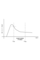
- FIG. 3 is a graph showing the output characteristics of a typical LLC resonant converter circuit.
- the operating frequency is controlled within a frequency range from a lower limit frequency fmin to an upper limit frequency fmax, which is higher than the resonant frequency.
- fmin lower limit frequency
- fmax upper limit frequency
- the present invention was made in consideration of these problems, and provides a control technology for an LLC resonant converter circuit that allows the output voltage to be continuously variable over a wide range.
- an LLC resonant converter circuit including a series resonant circuit, a drive circuit connected to the series resonant circuit and performing switching operations on a plurality of switching elements based on a drive signal, a transformer having a resonant coil constituting the series resonant circuit as a primary winding, and a rectifier circuit that rectifies and smoothes AC power generated in a secondary winding of the transformer, a control circuit for controlling a switching frequency at or above the resonant frequency of the series resonant circuit includes a frequency control terminal and a duty control terminal, and outputs a drive signal to the drive circuit indicating a switching frequency corresponding to the voltage level of the frequency control terminal and a duty ratio corresponding to the voltage level of the duty control terminal, and a control circuit for detecting an output voltage from the LLC resonant converter circuit and setting the output voltage.
- a control circuit for an LLC resonant converter circuit includes a detection circuit that stabilizes the voltage to a constant voltage level, a voltage divider circuit that divides the input voltage from a control power supply terminal and applies the divided voltage to the duty control terminal as a duty control voltage, and an adjustment circuit that is connected to the voltage divider circuit and the detection circuit and is capable of adjusting the duty control voltage and adjusting the frequency control voltage applied to the frequency control terminal based on the input voltage and the output voltage detected by the detection circuit, and the adjustment circuit varies the duty control voltage so that the duty ratio indicated by the drive signal increases and varies the frequency control voltage so that the switching frequency indicated by the drive signal decreases in response to switching from the input of a first instruction signal to the input of a second instruction signal.
- a series resonant circuit a drive circuit connected to the series resonant circuit and performing switching operations on a plurality of switching elements based on a drive signal
- a transformer having a resonant coil constituting the series resonant circuit as a primary winding, a rectifier circuit for rectifying and smoothing AC power generated in a secondary winding of the transformer, a drive control circuit including a frequency control terminal and a duty control terminal, and outputting to the drive circuit a drive signal indicating a switching frequency corresponding to the voltage level of the frequency control terminal and a duty ratio corresponding to the voltage level of the duty control terminal, a detection circuit for detecting an output voltage from the rectifier circuit and stabilizing the output voltage to a set voltage level, and a control power supply terminal for detecting an input power from a control power supply terminal.
- a control method for an LLC resonant converter circuit including a voltage divider circuit that divides a voltage and applies the divided voltage to the duty control terminal as a duty control voltage, and an adjustment circuit that is connected to the voltage divider circuit and the detection circuit and is capable of adjusting the duty control voltage and adjusting the frequency control voltage applied to the frequency control terminal based on the input power and the output voltage detected by the detection circuit, and that varies the duty control voltage so that the duty ratio of the drive signal increases and varies the frequency control voltage so that the switching frequency of the drive signal decreases in response to switching from the input of a first instruction signal to the input of a second instruction signal.
- the above-mentioned aspect provides a control technique for an LLC resonant converter circuit that allows the output voltage to be continuously variable over a wide range.
- FIG. 1 is a circuit diagram of an LLC resonant converter circuit (converter circuit) according to an embodiment.
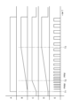
- 11 is a graph conceptually showing the change over time in voltage at points A, B, C, and D in the adjustment circuit, and the drive signal at point E. 1 is a graph showing output characteristics of a typical LLC resonant converter circuit.
- FIG. 1 is a circuit diagram of an LLC resonant converter circuit (hereinafter, sometimes abbreviated as a converter circuit) 1 according to an embodiment.
- the converter circuit 1 includes at least a primary side circuit 10 connected to a DC power source and including a series resonant circuit 11 , a transformer 3 , a secondary side circuit 20 that obtains AC power from the primary side circuit 10 via the transformer 3 , and a control circuit 30 .
- the primary side circuit 10 includes a series resonant circuit 11, switching elements Q11 and Q12, a drive circuit 13, a capacitor C10, an input capacitor C11, and the like.
- the primary side circuit 10 is connected to an external DC power supply via an input terminal (DCVin).
- the series resonant circuit 11 is formed by the primary coil Np of the transformer 3 and the resonant capacitor Cr, which are connected in series. For this reason, the primary coil Np can also be called a resonant coil.
- the switching elements Q11 and Q12 are controlled to perform a switching operation by a drive circuit 13.
- the switching operation of the switching elements Q11 and Q12 switches the direction of a current flowing through a resonant coil (primary coil Np) of the series resonant circuit 11.
- the switching elements Q11 and Q12 are, for example, field effect transistors (FETs), and an N-channel metal oxide semiconductor field effect transistor (MOSFET) is shown as an example in Fig. 1. For this reason, the switching elements Q11 and Q12 may be referred to as transistors Q11 and Q12.
- the drain of the transistor Q11 is connected to the input terminal (DCVin) of a DC power supply, the source of the transistor Q11 and the drain of the transistor Q12 are connected, and the source of the transistor Q12 is connected to a ground line from the ground terminal (GND).
- DCVin input terminal
- GND ground terminal
- the drive circuit 13 is connected to the transistors Q11 and Q12 so as to be able to apply a gate-source voltage (hereinafter, sometimes referred to as a VGS voltage) to the transistors Q11 and Q12.
- the drive circuit 13 alternately applies a VGS voltage exceeding a threshold voltage to the transistor Q11 and the transistor Q12 to alternately switch the on/off states of the transistor Q11 and the transistor Q12 (performs a switching operation).
- the drive circuit 13 switches the on/off states of the transistors Q11 and Q12 in accordance with the pulse period and duty ratio of the drive signals (VCOoutCH1 and VCOoutCH2) from the drive control circuit 50.
- the series resonant circuit 11 is connected to the source of the transistor Q11 and is provided between the drain and source of the transistor Q12.
- a load current can flow between the drain and source of the transistor Q11, the primary coil Np, and the resonant capacitor Cr
- a load current can flow through the resonant capacitor Cr, the primary coil Np, and between the drain and source of the transistor Q12 due to the power stored in the resonant capacitor Cr.
- the direction of the current flowing through the primary coil Np is switched by the switching operations of the transistors Q11 and Q12.
- the capacitor C10 absorbs voltage changes of the DC power supply connected between the input terminal (DCVin) and the ground terminal (GND).
- the input capacitor C11 is connected to the drain of the transistor Q1 and the source of the transistor Q2, that is, connected in parallel to the transistors Q11 and Q12, and smoothes the input voltage.
- the transformer 3 is composed of a primary coil Np and a secondary coil Ns, which are electrically insulated from each other, and a core, and magnetically couples the primary coil Np and the secondary coil Ns.
- Figure 1 does not show the excitation inductance (Lm) and leakage inductance (Lr) of the transformer 3, or parasitic elements such as the output capacitance and parasitic diodes of switching elements Q11 and Q12, which will be described later.
- the secondary circuit 20 includes output terminals (VOUT+) and (VOUT-), and outputs DC power from these output terminals. There are no particular restrictions on how the output DC power can be used. Loads with various characteristics can be connected to the output terminals.
- the secondary circuit 20 further includes a secondary coil Ns, which is the secondary winding of the transformer 3, and a rectifier circuit 21 that is connected to the secondary coil Ns and rectifies and smoothes the AC power generated in the secondary coil Ns.
- the rectifier circuit 21 includes a bridge rectifier circuit composed of rectifier diodes D21, D22, D23, and D24, and a capacitor C20. The AC power generated in the secondary coil Ns is converted to DC power by half-wave rectification by the bridge rectifier circuit and smoothing by the output capacitor C20.
- the control circuit 30 can control the switching frequency of the switching elements Q11 and Q12 to a frequency equal to or higher than the resonant frequency of the series resonant circuit 11, and can control the duty ratio of the switching operation of the switching elements Q11 and Q12. That is, the control circuit 30 can execute PFM (Pulse Frequency Modulation) control and PWM (Pulse Width Modulation) control, thereby making the output voltage from the converter circuit 1 (secondary side circuit 20) continuously variable over a wide range.
- PFM Pulse Frequency Modulation
- PWM Pulse Width Modulation
- wide range refers to a voltage range including a low output range of the converter output that is difficult to achieve by frequency control alone in a band higher than the resonant frequency in an LLC resonant converter circuit, and a high output range that can be achieved by frequency control alone.
- control circuit 30 adjusts the voltage level from a predetermined lower limit voltage level within a predetermined low voltage region and stabilizes it at a set voltage level.
- the set voltage level is set to a level higher than the predetermined low voltage region.
- the predetermined lower limit voltage level is set to zero, and the control circuit 30 adjusts the output voltage from the converter circuit 1 from zero and stabilizes it at the predetermined set voltage level.
- the predetermined lower limit voltage level is not limited to zero, and may be set to any voltage level within the predetermined low voltage region.
- the "predetermined low voltage region” here means a low output region of the converter output that is difficult to realize in an LLC resonant converter circuit only by frequency control in a band higher than the resonant frequency, and refers to a voltage region including zero.
- the predetermined low voltage region is, for example, a range from 0 (V) to 5 (V).
- the control circuit 30 includes a detection circuit 40, a drive control circuit 50, a voltage dividing circuit 60, an adjustment circuit 70, an input terminal block CN, and the like.
- the input terminal block CN includes a control power supply terminal (terminals 1 and 2), an instruction signal terminal (terminal 3), and a ground terminal (terminals 4, 5, and 6).
- the control power supply terminal receives a voltage supplied from a control power supply
- the indication signal terminal receives an off signal (corresponding to a first indication signal) or an on signal (corresponding to a second indication signal)
- the ground terminal is connected to a ground line.
- the drive control circuit 50 includes a frequency control terminal (VCOin terminal), a duty control terminal (DTin terminal), and output terminals for drive signals for two channels (VCOoutCH1 terminal, VCOoutCH2 terminal), and outputs a drive signal indicating a switching frequency corresponding to the voltage level of the frequency control terminal and a duty ratio corresponding to the voltage level of the duty control terminal to the drive circuit 13.
- VCOin terminal a frequency control voltage or VCO voltage
- the voltage applied to the duty control terminal may be referred to as a duty control voltage or DT voltage.
- the drive control circuit 50 is configured to lower the pulse frequency of the drive signal it outputs as the VCO voltage is higher within a specified range, to increase the pulse frequency of the drive signal it outputs as the VCO voltage is lower within that specified range, to increase the duty ratio of the drive signal it outputs as the DT voltage is higher within that specified range, and to decrease the duty ratio of the drive signal it outputs as the DT voltage is lower within that specified range.
- the drive control circuit 50 includes a frequency control terminal (VCOin terminal), a duty control terminal (DTin terminal), and output terminals for drive signals on two or more channels. As long as it is possible to control the pulse frequency and duty ratio of the drive signal as described above, there are no limitations on its specific configuration.
- the voltage divider circuit 60 divides the input voltage from the control power supply terminal of the input terminal block CN and applies the divided voltage to a duty control terminal (DTin terminal) of the drive control circuit 50 as a duty control voltage (DT voltage).
- the voltage dividing circuit 60 is composed of resistor elements R8 and R9 and a variable resistor VR2 connected in series between the control power supply terminal and the ground terminal, and a line leading to the duty control terminal of the drive control circuit 50 is connected between the resistor elements R8 and R9.
- the voltage input from the control power supply terminal is divided by the ratio of the resistance of the resistor element R8 to the combined resistance of the resistor elements R8 and R9 and the variable resistor VR2, and applied to the duty control terminal.
- the upper limit level of the DT voltage applied to the duty control terminal is determined by the resistance values of resistor elements R8 and R9 and variable resistor VR2, and corresponds to the upper limit of the duty ratio (upper limit duty ratio value) controlled by drive control circuit 50.
- voltage divider circuit 60 determines the upper limit level of the DT voltage that corresponds to the upper limit duty ratio value (maximum duty ratio).
- the detection circuit 40 detects the output voltage from the secondary circuit 20 and stabilizes the output voltage to a set voltage level.
- the detection circuit 40 includes capacitors Cd and Cf, resistor elements R41, R42, R43, R44, R45, R46, and R47, a variable resistor VR1, a shunt regulator IC, etc.
- Capacitor Cd and resistor elements R41 and R42 are connected in series between the output terminals (VOUT+) and (VOUT-) of the secondary circuit 20, and the series connection line of resistor element R43, variable resistor VR1, and resistor element R44 and the series connection line of resistor elements R46 and R47 and the shunt regulator IC are each connected in parallel to capacitor Cd.
- a branch line from the connection line between resistor element R47 and the cathode of the shunt regulator IC is connected to the slider terminal of variable resistor VR1 (terminal connected to the slider) via capacitor Cf and resistor element R45, which are connected in series.
- a line extending from the reference terminal of the shunt regulator IC is connected to the connection line between resistor element R45 and the slider terminal of variable resistor VR1.
- the variable resistor VR1 is provided to enable the set voltage level of the output voltage from the secondary circuit 20 (the voltage between the output terminals (VOUT+) (VOUT-)) to be adjusted in a voltage range higher than the specified low voltage range.
- the voltage applied to the slider of the variable resistor VR1 is controlled by the shunt regulator IC to be a reference voltage, so the output voltage is set by the resistance elements R43 and R44 and the resistance ratio of the variable resistor VR1 corresponding to the position of the slider. This allows the output voltage of the converter circuit 1 to be variably set.
- the resistance elements R43 and R44 and the variable resistor VR1 can be described as an output variable circuit that can variably set the voltage level of the output voltage from the converter circuit 1, and the level of the output voltage set by this output variable circuit is described as the set voltage level.
- the output voltage from the secondary side circuit 20 is detected across the capacitor Cd, and the detected output voltage is divided by the resistance elements R43 and R44 and the resistance of the variable resistor VR1 corresponding to the position of the slider and applied to the reference terminal of the shunt regulator IC, and the divided voltage is controlled to a reference voltage (e.g., 2.5 V). Therefore, the circuit including the shunt regulator IC, resistance elements R46 and R47, etc. can be described as a stabilization circuit that stabilizes the output voltage from the converter circuit 1 to a set voltage level by comparing the divided voltage of the detected output voltage with the reference voltage.
- a stabilization circuit that stabilizes the output voltage from the converter circuit 1 to a set voltage level by comparing the divided voltage of the detected output voltage with the reference voltage.
- the adjustment circuit 70 is connected to the voltage divider circuit 60 and the detection circuit 40, and is capable of adjusting the DT voltage applied to the duty control terminal (DTin terminal), and is also capable of adjusting the VCO voltage applied to the frequency control terminal (VCOin terminal) based on the input voltage from the control power supply terminal and the output voltage detected by the detection circuit 40.
- the adjustment circuit 70 includes photocouplers PC1 and PC2, a switching element QS, a rectifier diode D1, a capacitor Cs, resistor elements R1, R2, R3, R4, R5, and R6, and the like.
- the photocouplers are electrically insulated between the primary and secondary sides and are composed of a light emitting diode on the primary side and a phototransistor on the secondary side.
- Photocoupler PC1 is composed of a light emitting diode HD1 on the primary side and a phototransistor PQ1 on the secondary side
- photocoupler PC2 is composed of a light emitting diode HD2 on the primary side and a phototransistor PQ2 on the secondary side.
- the photocouplers PC1 and PC2 are turned on (the light emitting diodes HD1 and HD2 on the primary side are in a light emitting state) by application of an input voltage exceeding the non-light emitting forward voltage, and in the on state, the output impedance of the phototransistors PQ1 and PQ2 on the secondary side can be increased or decreased according to an increase or decrease in the current flowing through the light emitting diodes HD1 and HD2 on the primary side.
- the current flowing through the light emitting diodes on the primary side of the photocoupler may be referred to as the diode current of the photocoupler.
- the light-emitting diode HD1 of the photocoupler PC1 is connected in parallel to the resistor element R47. That is, the anode of the light-emitting diode HD1 is connected to the connection line between the resistor elements R46 and R47, and the cathode is connected to the connection point between the resistor element R47, the cathode of the shunt regulator IC, and the capacitor Cf.
- the phototransistor PQ1 of the photocoupler PC1 has a collector terminal connected to a connection line between the cathode of the rectifier diode D1 and the resistor element R3 (corresponding to the photocoupler output line), and an emitter terminal connected to the ground line.
- the light-emitting diode HD2 and the resistor elements R4 and R5 of the photocoupler PC2 are arranged in series on a line that extends from the control power supply terminal and connects to the ground line.
- the cathode of the light-emitting diode HD2 is connected to the resistor element R4, and the anode is connected to the resistor element R5.
- the light-emitting diode HD2 and the resistor elements R4 and R5 that are connected in series are also connected in parallel with the voltage divider circuit 60.
- the rectifier diode D1 and the resistor element R3 are connected in series to a branch line branched from the output line of the DT voltage from the voltage divider circuit 60 to the duty control terminal, and this branch line is connected to the connection line between the cathode of the light-emitting diode HD2 and the resistor element R4.
- the cathode of the rectifier diode D1 is connected to the resistor element R3, and the cathode of the light-emitting diode HD2 is connected to the connection line between the resistor elements R3 and R4.
- a capacitor Cs is provided between the duty control terminal and the ground line. The function of the capacitor Cs is to realize a soft start of the PFM control and PWM control by the control circuit 30.
- the phototransistor PQ2 and resistive element R6 of the photocoupler PC2 are arranged in series on a line that extends from the frequency control terminal and connects to the ground line.
- the collector terminal of the phototransistor PQ2 is connected to the frequency control terminal via the resistive element R6, and the emitter terminal is connected to the ground line.
- a branch line from the connection line between the collector terminal of the phototransistor PQ2 and the resistive element R6 is connected to the ground line via the resistive element R7.
- the switching element QS is turned on or off in response to an instruction signal input from an instruction signal terminal (terminal 3).
- the collector terminal of the switching element QS is connected to a line (photocoupler output line) extending from the collector terminal of the phototransistor PQ1, and the emitter terminal is connected to the ground line.
- the gate terminal of the switching element QS is connected to the ground line via a resistor R1, and is also connected to the instruction signal terminal (terminal 3) via a resistor R2 and a NOT circuit NT.
- the switching element QS may be, for example, a field effect transistor (FET), and may also be referred to as a transistor QS.
- the “duty ratio lower limit value” refers to a duty ratio value equal to or greater than zero that can bring the output voltage from the converter circuit 1 (secondary side circuit 20) to a predetermined lower limit voltage level, and in this embodiment, an example is shown in which the duty ratio lower limit value is set to zero.
- the control circuit 30 also includes capacitors C1 and C2. Capacitors C1 and C2 are arranged in parallel with each other between the line connected to the control power supply terminals (terminals 1 and 2) and the ground line connected to the ground terminals (terminals 4, 5, and 6), and smooth the input voltage from the control power supply terminals.
- the converter circuit 1 having such a circuit configuration operates as follows.
- the drive circuit 13 switches the on/off states of the transistors Q11 and Q12 in accordance with the pulse period and duty ratio of the drive signal from the drive control circuit 50. Specifically, the drive circuit 13 switches the on/off state of the transistor Q11 based on the drive signal output from the VCOoutCH1 terminal of the drive control circuit 50, and switches the on/off state of the transistor Q12 based on the drive signal output from the VCOoutCH2 terminal of the drive control circuit 50.
- the switching operation of the transistors Q11 and Q12 causes a resonant current to flow in the series resonant circuit 11, and AC power is induced in the secondary coil Ns of the transformer 3.
- the AC power generated in the secondary coil Ns is rectified and smoothed by the rectifier circuit 21, converted into DC power, and output.
- the detection circuit 40 detects the output voltage from the secondary side circuit 20 and stabilizes the output voltage to a set voltage level. Specifically, the output voltage from the secondary side circuit 20 is detected across the capacitor Cd, and the detected output voltage is divided by the resistance elements R43 and R44 and the resistance of the variable resistor VR1 corresponding to the position of the wiper, and applied to the reference terminal of the shunt regulator IC, and the divided voltage is controlled to be a reference voltage (e.g., 2.5 V).
- a reference voltage e.g. 2.5 V
- the diode current of the photocoupler PC1 increases, and when the voltage of the wiper of the variable resistor VR1 attempts to become lower than the reference voltage, the diode current of the photocoupler PC1 decreases.
- the output impedance on the secondary side increases or decreases according to the magnitude of the diode current on the primary side.
- the voltage of the resistive element R3 changes, and the diode current of the photocoupler PC2 changes, resulting in increasing or decreasing the VCO voltage applied to the frequency control terminal (VCOin terminal) of the drive control circuit 50.
- the voltage dividing circuit 60 the input voltage from the control power supply terminal is divided and applied to the duty control terminal (DTin terminal) of the drive control circuit 50 (DT voltage).
- the DT voltage applied to the duty control terminal and the VCO voltage applied to the frequency control terminal are adjusted by the adjustment circuit 70 in response to the on or off signal input from the instruction signal terminal.
- FIG. 2 is a graph conceptually showing the change over time in voltage at points A, B, C, and D in the adjustment circuit 70, and the drive signal at point E.
- the voltage at point C is equal to the voltage at the duty control terminal (DTin terminal)
- the voltage at point D is proportional to the voltage at the frequency control terminal (VCOin terminal).
- an OFF signal is input from the instruction signal terminal until timing T1, at which point the signal input from the instruction signal terminal switches from an OFF signal to an ON signal, and the ON signal continues to be input after timing T1.
- the OFF signal When an OFF signal is input, the OFF signal is inverted by the NOT circuit NT and input to the gate terminal of the transistor QS, turning the transistor QS on.
- the line (photocoupler output line) extending from the collector terminal of the phototransistor PQ1 and the cathode side of the rectifier diode D1 fall to the ground level.
- the voltage at point B becomes the ground level (0 V) and the voltage at point C becomes the lower limit.
- the drive signal output from the drive control circuit 50 shows a duty ratio of zero, and as a result, the output power from the converter circuit 1 becomes zero.
- the lower limit of the voltage at point C is determined by the forward voltage of the rectifier diode D1 and the collector-emitter saturation voltage of the transistor QS in the on-state, and corresponds to the DT voltage indicating the lower limit of the duty ratio (a duty ratio of zero in this embodiment).
- the diode current of photocoupler PC2 is at its maximum and the output impedance on the secondary side is at its minimum, so the voltage at point D is at its lower limit and the VCO voltage is also at its lower limit.
- the switching frequency indicated by the drive signal output from drive control circuit 50 is the upper limit frequency of the specified frequency range.
- the ON signal is inverted by the NOT circuit NT, so that the transistor QS is turned off.
- the transistor QS is turned off, the voltages at points B and C rise, and the DT voltage also rises, so the duty ratio indicated by the output drive signal increases.
- the voltage at point C rises with the time constant of the resistor element R8 and the capacitor Cs, and the voltage at point B also rises through the rectifier diode D1. As a result, the output power from the converter circuit 1 also increases.
- the adjustment circuit 70 in response to the input of an off signal (corresponding to a first instruction signal), sets the DT voltage to a voltage level corresponding to the lower limit of the duty ratio (zero duty ratio in this embodiment) and sets the VCO voltage to a voltage level corresponding to a predetermined high frequency (upper limit frequency) higher than the resonant frequency of the series resonant circuit 11, and in response to switching from the input of an off signal to the input of an on signal (corresponding to a second instruction signal), the adjustment circuit 70 fluctuates the DT voltage so that the duty ratio indicated by the drive signal increases and the VCO voltage so that the switching frequency indicated by the drive signal decreases.
- the duty ratio is set to a lower limit value (zero in this embodiment), so that the output voltage from the converter circuit 1 can be set to a predetermined lower limit voltage level (zero in this embodiment) that is difficult to achieve by frequency control alone in the LLC resonant converter circuit. Furthermore, by gradually increasing the duty ratio from the lower limit value, the output voltage from the converter circuit 1 can be gradually increased from the predetermined lower limit voltage level, and thus the output voltage can be adjusted from the predetermined lower limit voltage level in a low voltage region including zero and stabilized at a set voltage level.
- the C point voltage and DT voltage gradually rise from time T1, and reach their upper limit levels at time T2. As a result, after time T2, the duty ratio indicated by the drive signal also reaches its upper limit (maximum duty ratio).
- the upper limit levels of the C point and DT voltage are determined by the resistance values of the resistive elements R8 and R9 and the variable resistor VR2.
- the rise time of the C point voltage and DT voltage (the time from time T1 to time T2) is determined by the time constant of the resistive element R8 and the capacitor Cs, and this time is the period during which PWM control (duty ratio control) is executed.
- the voltage at point B continues to rise even after the voltage at point C and the DT voltage reach their upper limits.
- the voltage at point D and the VCO voltage continue to rise, and as a result, the switching frequency indicated by the output drive signal is controlled to decrease from the upper limit frequency.
- the duty ratio indicated by the drive signal is at the upper limit, and the output voltage from the converter circuit 1 increases.
- the output voltage detected by the detection circuit 40 rises, and when the voltage of the wiper of the variable resistor VR1 becomes higher than the reference voltage, the diode current of the photocoupler PC1 starts to increase, causing the secondary output impedance to start to decrease, limiting the increase in the voltage at point B. Accordingly, the action of the photocoupler PC2 also limits the increases in the voltage at point D and the VCO voltage, and as a result, the decrease in the switching frequency indicated by the output drive signal is also limited. 2, after which the fluctuation in the switching frequency is stabilized and the output voltage from the converter circuit 1 is stabilized at a predetermined set voltage level. In other words, the time from timing T1 to timing T3 is the period during which PFM control is executed.
- the adjustment circuit 70 suppresses fluctuations in the frequency control voltage (VCO voltage) when the divided voltage (the voltage of the wiper of the variable resistor VR1) becomes higher than the reference voltage. That is, in this embodiment, the output is controlled to a constant set voltage by PFM control in a certain high output range. Therefore, according to this embodiment, the output voltage from the converter circuit 1 can be adjusted from a predetermined lower limit voltage level within the low voltage region, which includes zero, and stabilized at a set voltage level higher than the low voltage region.
- the C point voltage and DT voltage gradually increase from timing T1 and are limited at the upper limit level from timing T2 onwards
- the D point voltage and VCO voltage gradually increase from timing T1 and continue to increase after timing T2 and are limited at timing T3.
- the duty ratio indicated by the drive signal becomes the upper limit value (maximum duty ratio) from timing T2 onwards
- the switching frequency indicated by the drive signal becomes the lower limit value (frequency higher than the resonant frequency) from timing T3 onwards.
- the adjustment circuit 70 is configured so that a first change time of the duty control voltage (DT voltage) accompanying a switch from the input of a first instruction signal (off signal) to the input of a second instruction signal (on signal) is shorter than a second change time of the frequency control voltage (VCO voltage) accompanying the switch, the first change time being the time required to change the duty control voltage (DT voltage) from a voltage level corresponding to the lower limit value of the duty ratio (zero duty ratio in this embodiment) to a voltage level corresponding to the upper limit value of the duty ratio, and the second change time being the time required for the frequency control voltage (VCO voltage) to change from a voltage level corresponding to a predetermined high frequency (upper limit frequency) and be suppressed.
- the timing at which the frequency control voltage (VCO voltage) is suppressed approaches the timing at which the output voltage reaches a predetermined set voltage level.
- FIG. 1 shows an example of a configuration in which switching elements Q11 and Q12 are connected in a half-bridge configuration, but this can also be modified to a configuration in which four switching elements are connected in a full-bridge configuration.
- the drive control circuit 50 may have output terminals for drive signals for four channels, or may have output terminals for drive signals for two channels.
- the drive circuit 13 may control the operation of the switching elements corresponding to each channel in response to the drive signal for that channel.
- the drive circuit 13 may control the operation of the switching element pair corresponding to one channel in response to the drive signal for that channel.
- the above embodiment may be modified so that the switching element QS is turned on by inputting an ON signal, and turned off by inputting an OFF signal.
- the NOT circuit NT is not required.
- the above-described embodiment may be modified so that the drive control circuit 50 outputs a drive signal indicating a lower duty ratio as the DT voltage is higher within a predetermined range, and outputs a drive signal indicating a higher duty ratio as the DT voltage is lower within a predetermined range.
- the drive control circuit 50 may also be configured to output a drive signal indicating a higher switching frequency as the VCO voltage is higher within a predetermined range, and outputs a drive signal indicating a lower switching frequency as the VCO voltage is lower within the predetermined range.
- the adjustment circuit 70 may be configured to lower the DT voltage so that the duty ratio indicated by the drive signal increases and to lower the VCO voltage so that the switching frequency indicated by the drive signal decreases in response to switching from the input of the first instruction signal (off signal) to the input of the second instruction signal (on signal).
- a control circuit for controlling a switching frequency at or above a resonant frequency of the series resonant circuit in an LLC resonant converter circuit including a series resonant circuit, a drive circuit connected to the series resonant circuit and performing switching operations on a plurality of switching elements based on a drive signal, a transformer having a resonant coil constituting the series resonant circuit as a primary winding, and a rectifier circuit rectifying and smoothing AC power generated in a secondary winding of the transformer, comprising: a drive control circuit including a frequency control terminal and a duty control terminal, and outputting to the drive circuit a drive signal indicating a switching frequency corresponding to a voltage level of the frequency control terminal and a duty ratio corresponding to the voltage level of the duty control terminal; a detection circuit for detecting an output voltage from the LLC resonant converter circuit and stabilizing the output voltage to a set voltage level; a voltage dividing circuit which divides an input voltage from a control power supply terminal and applies the
- the adjustment circuit sets the duty control voltage to a voltage level corresponding to a duty ratio lower limit value and sets the frequency control voltage to a voltage level corresponding to a predetermined high frequency higher than the resonant frequency in response to the input of the first instruction signal.
- the detection circuit includes: an output variable circuit capable of variably setting a voltage level of an output voltage from the LLC resonant converter circuit; a stabilization circuit that stabilizes the output voltage from the LLC resonant converter circuit to the set voltage level set by the output variable circuit by comparing a divided voltage of the detected output voltage with a reference voltage; Including, the adjustment circuit suppresses a fluctuation in the frequency control voltage when the divided voltage is about to become higher than the reference voltage in a state in which the second instruction signal is input.
- the adjustment circuit is configured so that a first change time of the duty control voltage accompanying a switch from the input of the first instruction signal to the input of the second instruction signal is shorter than a second change time of the frequency control voltage accompanying the switch;
- the first change time is a time required for changing the duty control voltage from a voltage level corresponding to the duty ratio lower limit value to a voltage level corresponding to the duty ratio upper limit value
- the second change time is a time period during which the frequency control voltage changes from a voltage level corresponding to the predetermined high frequency to be suppressed.
- the adjustment circuit includes: a first light-emitting diode through which a current flows when the divided voltage becomes higher than the reference voltage; a first phototransistor constituting a first photocoupler together with the first light emitting diode; a rectifier diode and a first resistor element provided in series on a branch line that branches off from an output line of the duty control voltage from the voltage dividing circuit to the duty control terminal and is connected to a ground line; a second resistor element and a second light-emitting diode connected in parallel with the voltage divider circuit to a line extending from the control power supply terminal and connected to a ground line; a second phototransistor constituting a second photocoupler together with the second light emitting diode; Including, a line in which the second light-emitting diode and the second resistor element are connected in series is connected to the branch line on the cathode side of the second light-emitting diode; the second phototransistor is provided on a line
- the adjustment circuit further includes a switching element having an emitter terminal connected to a ground line and a collector terminal connected to the photocoupler output line, the switching element being turned on in response to an input of the first instruction signal and turned off in response to an input of the second instruction signal;
- the switching element When the switching element is turned on, the photocoupler output line and the cathode side of the rectifier diode fall to the ground level, so that the duty control voltage applied to the duty control terminal becomes a voltage level corresponding to the duty ratio lower limit value.
- a control circuit according to any one of ⁇ 1> to ⁇ 6>;
- An LLC resonant converter circuit comprising: ⁇ 8> A series resonant circuit; a drive circuit connected to the series resonant circuit and configured to perform switching operations on a plurality of switching elements based on a drive signal; a transformer having a primary winding that is a resonant coil that constitutes the series resonant circuit; a rectifier circuit that rectifies and smoothes the AC power generated in the secondary winding of the transformer; a drive control circuit including a frequency control terminal and a duty control terminal, and outputting to the drive circuit a drive signal indicating a switching frequency corresponding to a voltage level of the frequency control terminal and a duty ratio corresponding to the voltage level of the duty control terminal; a detection circuit that detects an output voltage from the rectifier circuit and stabilizes the output voltage to a set voltage level; a voltage dividing circuit which
- the method for controlling the LLC resonant converter circuit according to ⁇ 8> further comprises: ⁇ 10> the detection circuit includes an output variable circuit capable of variably setting a voltage level of an output voltage from the LLC resonant converter circuit, and a stabilization circuit that stabilizes the output voltage from the LLC resonant converter circuit to the set voltage level set by the output variable circuit by comparing a divided voltage of the detected output voltage with a reference voltage; suppressing a fluctuation in the frequency control voltage when the divided voltage is about to become higher than the reference voltage in a state in which the second instruction signal is input;
Landscapes
- Engineering & Computer Science (AREA)
- Power Engineering (AREA)
- Dc-Dc Converters (AREA)
Abstract
Description
図3の例では、共振周波数よりも高い下限周波数fminから上限周波数fmaxまでの周波数範囲で動作周波数が制御されている。
ところが、一般的なLLC共振コンバータ回路では、図3に示されるように、動作周波数をいくら高くしたとしても、コンバータ出力を或るレベルより低くすることは難しい。
図1は、実施形態に係るLLC共振コンバータ回路(以降、コンバータ回路と略称する場合もある)1の回路図である。
コンバータ回路1は、直流電源に接続され直列共振回路11を含む一次側回路10、トランス3、一次側回路10からトランス3を介して交流電力を得る二次側回路20、及び制御回路30を少なくとも備える。
一次側回路10は、入力端子(DCVin)を介して外部の直流電源と接続されている。
スイッチング素子Q11及びQ12には、例えばFET(Field Effect Transistor)が利用され、図1には、Nチャンネル型のMOSFET(Metal Oxide Semiconductor Field Effect Transistor)が例示されている。このため、スイッチング素子Q11及びQ12はトランジスタQ11及びQ12と表記する場合もある。
このように図1では、ハーフブリッジ方式で接続されるスイッチング素子Q11及びQ12が例示されているが、フルブリッジ方式で接続される2以上のスイッチング素子に置き換えることも可能である。
ドライブ回路13は、トランジスタQ11及びトランジスタQ12に対して交互に閾値電圧を超えるVGS電圧を印加することで、トランジスタQ11及びトランジスタQ12のオンオフ状態を交互にスイッチングさせる(スイッチング動作させる)。このとき、ドライブ回路13は、ドライブ制御回路50からのドライブ信号(VCOoutCH1及びVCOoutCH2)のパルス周期及びデューティー比に合わせてトランジスタQ11及びQ12のオンオフ状態をスイッチングさせる。
このようにトランジスタQ11及びQ12のスイッチング動作により一次側コイルNpに流れる電流の向きが切り替えられる。
入力コンデンサC11は、トランジスタQ1のドレインとトランジスタQ2のソースとに接続、即ちトランジスタQ11及びQ12に対して並列に接続されており、入力電圧を平滑化する。
ここで「広範囲」とは、LLC共振コンバータ回路において共振周波数よりも高い帯域での周波数制御のみでは実現することが難しいコンバータ出力の低出力域、及び当該周波数制御のみで実現可能な高出力域を含む電圧範囲である。
ここでの「所定低電圧領域」とは、LLC共振コンバータ回路において共振周波数よりも高い帯域での周波数制御のみでは実現することが難しいコンバータ出力の低出力域であって、ゼロを含む電圧領域を意味する。効率が著しく悪い或いは回路素子が損失するような非実用的な設計条件ではない通常の設計条件で動作する出力電力500ワット(W)以上のLLC共振コンバータ回路において、当該所定低電圧領域は、例えば、0(V)以上5(V)以下の範囲となる。
図1の例において入力端子台CNは、制御電源端子(1番端子及び2番端子)、指示信号端子(3番端子)及びグランド端子(4番端子、5番端子及び6番端子)を含む。
制御電源端子には制御電源から供給される電圧が入力され、指示信号端子にはオフ信号(第一指示信号に相当)又はオン信号(第二指示信号に相当)が入力され、グランド端子にはグランドラインが接続される。
ドライブ制御回路50は、周波数制御端子(VCOin端子)、デューティー制御端子(DTin端子)並びに2チャンネル以上のドライブ信号の出力端子を含んでおり、上述のようにドライブ信号のパルス周波数及びデューティー比を制御可能であれば、その具体的構成は何ら限定されない。
図1の例では、分圧回路60は、制御電源端子とグランド端子との間に直列に接続された抵抗素子R8及びR9並びに可変抵抗器VR2から構成されており、抵抗素子R8と抵抗素子R9との間にドライブ制御回路50のデューティー制御端子に繋がるラインが接続されている。これにより、制御電源端子から入力される電圧が抵抗素子R8及びR9並びに可変抵抗器VR2の合成抵抗に対する抵抗素子R8の抵抗の比で分圧されてデューティー制御端子に印加される。
図1の例において調整回路70は、フォトカプラPC1及びPC2、スイッチング素子QS、整流ダイオードD1、コンデンサCs、抵抗素子R1、R2、R3、R4、R5及びR6等を含む。
フォトカプラPC1及びPC2はそれぞれ、非発光順電圧を超える入力電圧の印加によってオン状態(一次側の発光ダイオードHD1及びHD2の発光状態)となり、オン状態において一次側の発光ダイオードHD1及びHD2に流れる電流の増減に応じて二次側のフォトトランジスタPQ1及びPQ2の出力インピーダンスを増減させることができる。以降の説明では、フォトカプラの一次側の発光ダイオードに流れる電流をフォトカプラのダイオード電流と表記する場合がある。
フォトカプラPC1のフォトトランジスタPQ1は、コレクタ端子が整流ダイオードD1のカソードと抵抗素子R3との接続ラインに接続されており(フォトカプラ出力ラインに相当)、エミッタ端子がグランドラインに接続されている。
また、デューティー制御端子とグランドラインとの間にコンデンサCsが設けられている。コンデンサCsの作用により制御回路30によるPFM制御及びPWM制御のソフトスタートが実現される。
スイッチング素子QSには、例えばFET(Field Effect Transistor)が利用され、スイッチング素子QSはトランジスタQSと表記する場合もある。
トランジスタQSがオン状態になると、フォトトランジスタPQ1のコレクタ端子から延びるライン(フォトカプラ出力ライン)及び整流ダイオードD1のカソード側がグランドレベルに落ちることになる。結果、後述するように、デューティー制御端子に印加されるDT電圧がデューティー比下限値に対応する電圧レベルとなる。
ここで「デューティー比下限値」とは、コンバータ回路1(二次側回路20)からの出力電圧を所定下限電圧レベルとすることができるデューティー比のゼロ以上の値を示し、本実施形態では、デューティー比下限値がゼロとされる例が示される。
コンデンサC1及びC2は、制御電源端子(1番端子及び2番端子)に繋がるラインとグランド端子(4番端子、5番端子及び6番端子)に繋がるグランドラインとの間に相互に並列に設けられており、制御電源端子からの入力電圧を平滑化する。
このような回路構成を有するコンバータ回路1は次のように動作する。
ドライブ回路13は、ドライブ制御回路50からのドライブ信号のパルス周期及びデューティー比に合わせてトランジスタQ11及びQ12のオンオフ状態をスイッチングさせる。具体的には、ドライブ回路13は、ドライブ制御回路50のVCOoutCH1端子から出力されるドライブ信号に基づいてトランジスタQ11のオンオフ状態をスイッチングさせ、ドライブ制御回路50のVCOoutCH2端子から出力されるドライブ信号に基づいてトランジスタQ12のオンオフ状態をスイッチングさせる。
これにより可変抵抗器VR1の摺動子の電圧が基準電圧よりも高くなろうとすると、フォトカプラPC1のダイオード電流が大きくなり、可変抵抗器VR1の摺動子の電圧が基準電圧よりも低くなろうとすると、フォトカプラPC1のダイオード電流が小さくなる。
一方で、分圧回路60では、制御電源端子からの入力電圧が分圧されてドライブ制御回路50のデューティー制御端子(DTin端子)に印加される(DT電圧)。
トランジスタQSがオン状態では、フォトトランジスタPQ1のコレクタ端子から延びるライン(フォトカプラ出力ライン)及び整流ダイオードD1のカソード側がグランドレベルに落ちる。これにより、B点の電圧はグランドレベル(0V)となり、C点の電圧は下限値となる。そしてドライブ制御回路50から出力されるドライブ信号はデューティー比ゼロを示し、結果、コンバータ回路1からの出力電力はゼロとなる。
ここで、図1の例においてC点の電圧の下限値は、整流ダイオードD1の順方向電圧及びオン状態のトランジスタQSのコレクタエミッタ間飽和電圧によって定まり、デューティー比下限値(本実施形態ではデューティー比ゼロ)を示すDT電圧に対応する。
トランジスタQSがオフ状態となることで、B点及びC点の電圧が上昇し、DT電圧も上昇することから、出力されるドライブ信号が示すデューティー比は増加していく。ここで、C点の電圧は抵抗素子R8及びコンデンサCsの時定数で上昇し、B点の電圧も整流ダイオードD1を通じて上昇する。結果、コンバータ回路1からの出力電力も増加していくことになる。
このときD点の電圧及びVCO電圧もなお上昇していき、結果、出力されるドライブ信号が示すスイッチング周波数についても上限周波数から低下する方向で制御される。このとき、そのドライブ信号が示すデューティー比は上限値となっており、コンバータ回路1からの出力電圧は上昇していく。
このタイミングは、図2のグラフにおいてタイミングT3で示されており、以降、スイッチング周波数の変動が安定化されて、コンバータ回路1からの出力電圧が所定の設定電圧レベルで安定化される。つまり、タイミングT1からタイミングT3までの時間は、PFM制御が実行される期間となる。
従って、本実施形態によれば、コンバータ回路1からの出力電圧をゼロを含む当該低電圧領域内の所定下限電圧レベルから調整し、当該低電圧領域よりも高い設定電圧レベルで安定化させることができる。
なお、周波数制御電圧(VCO電圧)が抑制されるタイミングは、出力電圧が所定の設定電圧レベルに到達したタイミングに近似する。
上述の実施形態の内容は適宜変形可能である。即ち、本実施形態は、図1に例示される回路構成に限定されない。
直列共振回路と、該直列共振回路に接続されておりドライブ信号に基づいて複数のスイッチング素子をスイッチング動作させるドライブ回路と、該直列共振回路を構成する共振コイルを一次巻線とするトランスと、該トランスの二次巻線に生じた交流電力を整流及び平滑化する整流回路とを含むLLC共振コンバータ回路において、該直列共振回路の共振周波数以上でスイッチング周波数を制御する制御回路であって、
周波数制御端子及びデューティー制御端子を含み、該周波数制御端子の電圧レベルに対応するスイッチング周波数及び該デューティー制御端子の電圧レベルに対応するデューティー比を示すドライブ信号を前記ドライブ回路へ出力するドライブ制御回路と、
前記LLC共振コンバータ回路からの出力電圧を検出して該出力電圧が設定電圧レベルとなるように安定化させる検出回路と、
制御電源端子からの入力電圧を分圧してデューティー制御電圧として前記デューティー制御端子に印加する分圧回路と、
前記分圧回路及び前記検出回路に接続されており、前記デューティー制御電圧を調整可能であると共に、前記入力電圧及び前記検出回路で検出される出力電圧に基づいて前記周波数制御端子に印加される周波数制御電圧を調整可能である調整回路と、
を備え、
前記調整回路は、第一指示信号の入力から第二指示信号の入力への切り替えに応じて、前記ドライブ信号が示すデューティー比が上がるように前記デューティー制御電圧を変動させかつ前記ドライブ信号が示すスイッチング周波数が下がるように前記周波数制御電圧を変動させる、
LLC共振コンバータ回路の制御回路。
<2>
前記調整回路は、前記第一指示信号の入力に応じて、前記デューティー制御電圧をデューティー比下限値に対応する電圧レベルにしかつ前記周波数制御電圧を前記共振周波数よりも高い所定高周波数に対応する電圧レベルにする、
<1>に記載のLLC共振コンバータ回路の制御回路。
<3>
前記検出回路は、
前記LLC共振コンバータ回路からの出力電圧の電圧レベルを可変に設定可能な出力可変回路と、
検出された出力電圧の分圧電圧と基準電圧との比較により、前記LLC共振コンバータ回路からの出力電圧を前記出力可変回路により設定された前記設定電圧レベルとなるように安定化させる安定化回路と、
を含み、
前記調整回路は、前記第二指示信号が入力された状態において、前記分圧電圧が前記基準電圧よりも高くなろうとした場合に前記周波数制御電圧の変動を抑制する、
<2>に記載のLLC共振コンバータ回路の制御回路。
<4>
前記調整回路は、前記第一指示信号の入力から第二指示信号の入力への切り替えに伴う前記デューティー制御電圧の第一変動時間が該切り替えに伴う前記周波数制御電圧の第二変動時間よりも短くなるように構成されており、
前記第一変動時間は、前記デューティー制御電圧を前記デューティー比下限値に対応する電圧レベルからデューティー比上限値に対応する電圧レベルまで変動させるのに要する時間であり、
前記第二変動時間は、前記周波数制御電圧が前記所定高周波数に対応する電圧レベルから変動して抑制されるまでの時間である、
<3>に記載のLLC共振コンバータ回路の制御回路。
<5>
前記調整回路は、
前記分圧電圧が前記基準電圧よりも高くなろうとした場合に流れる電流が大きくなる第一発光ダイオードと、
前記第一発光ダイオードと共に第一フォトカプラを構成する第一フォトトランジスタと、
前記分圧回路から前記デューティー制御端子への前記デューティー制御電圧の出力ラインから分岐してグランドラインへ繋がる分岐ラインに直列に設けられた整流ダイオード及び第一抵抗素子と、
前記制御電源端子から延びてグランドラインへと繋がるラインに前記分圧回路と並列に接続される第二抵抗素子及び第二発光ダイオードと、
前記第二発光ダイオードと共に第二フォトカプラを構成する第二フォトトランジスタと、
を含み、
前記第二発光ダイオード及び前記第二抵抗素子が直列に設けられたラインが前記第二発光ダイオードのカソード側で前記分岐ラインと接続されており、
前記周波数制御端子から延びてグランドラインへと繋がるラインに前記第二フォトトランジスタが設けられており、
前記第一フォトトランジスタのエミッタ端子はグランドラインに接続されており、
前記第一フォトトランジスタのコレクタ端子から延びるフォトカプラ出力ラインが前記分岐ラインにおける前記整流ダイオードのカソードと前記第一抵抗素子との間に接続されている、
<3>又は<4>に記載のLLC共振コンバータ回路の制御回路。
<6>
前記調整回路は、エミッタ端子がグランドラインに接続されており、コレクタ端子が前記フォトカプラ出力ラインに接続されており、前記第一指示信号の入力に応じてオン状態となり前記第二指示信号の入力に応じてオフ状態となるスイッチング素子を更に含み、
前記スイッチング素子がオン状態になると、前記フォトカプラ出力ライン及び前記整流ダイオードのカソード側がグランドレベルに落ちることで、前記デューティー制御端子に印加される前記デューティー制御電圧が前記デューティー比下限値に対応する電圧レベルになる、
<5>に記載のLLC共振コンバータ回路の制御回路。
<7>
<1>から<6>のいずれか一つに記載の制御回路と、
前記直列共振回路と、
前記ドライブ回路と、
前記トランスと、
前記整流回路と、
を備えるLLC共振コンバータ回路。
<8>
直列共振回路と、
前記直列共振回路に接続されておりドライブ信号に基づいて複数のスイッチング素子をスイッチング動作させるドライブ回路と、
前記直列共振回路を構成する共振コイルを一次巻線とするトランスと、
前記トランスの二次巻線に生じた交流電力を整流及び平滑化する整流回路と、
周波数制御端子及びデューティー制御端子を含み、該周波数制御端子の電圧レベルに対応するスイッチング周波数及び該デューティー制御端子の電圧レベルに対応するデューティー比を示すドライブ信号を前記ドライブ回路へ出力するドライブ制御回路と、
前記整流回路からの出力電圧を検出して該出力電圧が設定電圧レベルとなるように安定化させる検出回路と、
制御電源端子からの入力電力の電圧を分圧してデューティー制御電圧として前記デューティー制御端子に印加する分圧回路と、
前記分圧回路及び前記検出回路に接続されており、前記デューティー制御電圧を調整可能であると共に、前記入力電力及び前記検出回路で検出される出力電圧に基づいて前記周波数制御端子に印加される周波数制御電圧を調整可能である調整回路と、
を備えるLLC共振コンバータ回路の制御方法であって、
第一指示信号の入力から第二指示信号の入力への切り替えに応じて、前記ドライブ信号の前記デューティー比が上がるように前記デューティー制御電圧を変動させかつ前記ドライブ信号の前記スイッチング周波数が下がるように前記周波数制御電圧を変動させる、
LLC共振コンバータ回路の制御方法。
<9>
前記第一指示信号の入力に応じて、前記デューティー制御電圧をデューティー比下限値に対応する電圧レベルにしかつ前記周波数制御電圧を前記直列共振回路の共振周波数よりも高い所定高周波数に対応する電圧レベルにする、
ことを更に含む<8>に記載のLLC共振コンバータ回路の制御方法。
<10>
前記検出回路は、前記LLC共振コンバータ回路からの出力電圧の電圧レベルを可変に設定可能な出力可変回路と、検出された出力電圧の分圧電圧と基準電圧との比較により、前記LLC共振コンバータ回路からの出力電圧を前記出力可変回路により設定された前記設定電圧レベルとなるように安定化させる安定化回路とを含み、
前記第二指示信号が入力された状態において、前記分圧電圧が前記基準電圧よりも高くなろうとした場合に前記周波数制御電圧の変動を抑制する、
ことを更に含む<9>に記載のLLC共振コンバータ回路の制御方法。
<11>
前記第一指示信号の入力から第二指示信号の入力への切り替えに伴う前記デューティー制御電圧の第一変動時間が該切り替えに伴う前記周波数制御電圧の第二変動時間よりも短く、
前記第一変動時間は、前記デューティー制御電圧を前記デューティー比下限値に対応する電圧レベルからデューティー比上限値に対応する電圧レベルまで変動させるのに要する時間であり、
前記第二変動時間は、前記周波数制御電圧が前記所定高周波数に対応する電圧レベルから変動して抑制されるまでの時間である、
<10>に記載のLLC共振コンバータ回路の制御方法。
3 トランス
10 一次側回路
11 直列共振回路
13 ドライブ回路
20 二次側回路
21 整流回路
30 制御回路
40 検出回路
50 ドライブ制御回路
60 分圧回路
70 調整回路
VR1、VR2 可変抵抗器
IC シャントレギュレータ
PC1、PC2 フォトカプラ
QS、Q11、Q12 スイッチング素子(トランジスタ)
NT NOT回路
HD1、HD2 発光ダイオード
PQ1、PQ2 フォトトランジスタ
Claims (11)
- 直列共振回路と、該直列共振回路に接続されておりドライブ信号に基づいて複数のスイッチング素子をスイッチング動作させるドライブ回路と、該直列共振回路を構成する共振コイルを一次巻線とするトランスと、該トランスの二次巻線に生じた交流電力を整流及び平滑化する整流回路とを含むLLC共振コンバータ回路における、該直列共振回路の共振周波数以上でスイッチング周波数を制御する制御回路であって、
周波数制御端子及びデューティー制御端子を含み、該周波数制御端子の電圧レベルに対応するスイッチング周波数及び該デューティー制御端子の電圧レベルに対応するデューティー比を示すドライブ信号を前記ドライブ回路へ出力するドライブ制御回路と、
前記LLC共振コンバータ回路からの出力電圧を検出して該出力電圧が設定電圧レベルとなるように安定化させる検出回路と、
制御電源端子からの入力電圧を分圧してデューティー制御電圧として前記デューティー制御端子に印加する分圧回路と、
前記分圧回路及び前記検出回路に接続されており、前記デューティー制御電圧を調整可能であると共に、前記入力電圧及び前記検出回路で検出される出力電圧に基づいて前記周波数制御端子に印加される周波数制御電圧を調整可能である調整回路と、
を備え、
前記調整回路は、第一指示信号の入力から第二指示信号の入力への切り替えに応じて、前記ドライブ信号が示すデューティー比が上がるように前記デューティー制御電圧を変動させかつ前記ドライブ信号が示すスイッチング周波数が下がるように前記周波数制御電圧を変動させる、
LLC共振コンバータ回路の制御回路。 - 前記調整回路は、前記第一指示信号の入力に応じて、前記デューティー制御電圧をデューティー比下限値に対応する電圧レベルにしかつ前記周波数制御電圧を前記共振周波数よりも高い所定高周波数に対応する電圧レベルにする、
請求項1に記載のLLC共振コンバータ回路の制御回路。 - 前記検出回路は、
前記LLC共振コンバータ回路からの出力電圧の電圧レベルを可変に設定可能な出力可変回路と、
検出された出力電圧の分圧電圧と基準電圧との比較により、前記LLC共振コンバータ回路からの出力電圧を前記出力可変回路により設定された前記設定電圧レベルとなるように安定化させる安定化回路と、
を含み、
前記調整回路は、前記第二指示信号が入力された状態において、前記分圧電圧が前記基準電圧よりも高くなろうとした場合に前記周波数制御電圧の変動を抑制する、
請求項2に記載のLLC共振コンバータ回路の制御回路。 - 前記調整回路は、前記第一指示信号の入力から第二指示信号の入力への切り替えに伴う前記デューティー制御電圧の第一変動時間が該切り替えに伴う前記周波数制御電圧の第二変動時間よりも短くなるように構成されており、
前記第一変動時間は、前記デューティー制御電圧を前記デューティー比下限値に対応する電圧レベルからデューティー比上限値に対応する電圧レベルまで変動させるのに要する時間であり、
前記第二変動時間は、前記周波数制御電圧が前記所定高周波数に対応する電圧レベルから変動して抑制されるまでの時間である、
請求項3に記載のLLC共振コンバータ回路の制御回路。 - 前記調整回路は、
前記分圧電圧が前記基準電圧よりも高くなろうとした場合に流れる電流が大きくなる第一発光ダイオードと、
前記第一発光ダイオードと共に第一フォトカプラを構成する第一フォトトランジスタと、
前記分圧回路から前記デューティー制御端子への前記デューティー制御電圧の出力ラインから分岐してグランドラインへ繋がる分岐ラインに直列に設けられた整流ダイオード及び第一抵抗素子と、
前記制御電源端子から延びてグランドラインへと繋がるラインに前記分圧回路と並列に接続される第二抵抗素子及び第二発光ダイオードと、
前記第二発光ダイオードと共に第二フォトカプラを構成する第二フォトトランジスタと、
を含み、
前記第二発光ダイオード及び前記第二抵抗素子が直列に設けられたラインが前記第二発光ダイオードのカソード側で前記分岐ラインと接続されており、
前記周波数制御端子から延びてグランドラインへと繋がるラインに前記第二フォトトランジスタが設けられており、
前記第一フォトトランジスタのエミッタ端子はグランドラインに接続されており、
前記第一フォトトランジスタのコレクタ端子から延びるフォトカプラ出力ラインが前記分岐ラインにおける前記整流ダイオードのカソードと前記第一抵抗素子との間に接続されている、
請求項3又は4に記載のLLC共振コンバータ回路の制御回路。 - 前記調整回路は、エミッタ端子がグランドラインに接続されており、コレクタ端子が前記フォトカプラ出力ラインに接続されており、前記第一指示信号の入力に応じてオン状態となり前記第二指示信号の入力に応じてオフ状態となるスイッチング素子を更に含み、
前記スイッチング素子がオン状態になると、前記フォトカプラ出力ライン及び前記整流ダイオードのカソード側がグランドレベルに落ちることで、前記デューティー制御端子に印加される前記デューティー制御電圧が前記デューティー比下限値に対応する電圧レベルになる、
請求項5に記載のLLC共振コンバータ回路の制御回路。 - 請求項1から6のいずれか一項に記載の制御回路と、
前記直列共振回路と、
前記ドライブ回路と、
前記トランスと、
前記整流回路と、
を備えるLLC共振コンバータ回路。 - 直列共振回路と、
前記直列共振回路に接続されておりドライブ信号に基づいて複数のスイッチング素子をスイッチング動作させるドライブ回路と、
前記直列共振回路を構成する共振コイルを一次巻線とするトランスと、
前記トランスの二次巻線に生じた交流電力を整流及び平滑化する整流回路と、
周波数制御端子及びデューティー制御端子を含み、該周波数制御端子の電圧レベルに対応するスイッチング周波数及び該デューティー制御端子の電圧レベルに対応するデューティー比を示すドライブ信号を前記ドライブ回路へ出力するドライブ制御回路と、
前記整流回路からの出力電圧を検出して該出力電圧が設定電圧レベルとなるように安定化させる検出回路と、
制御電源端子からの入力電力の電圧を分圧してデューティー制御電圧として前記デューティー制御端子に印加する分圧回路と、
前記分圧回路及び前記検出回路に接続されており、前記デューティー制御電圧を調整可能であると共に、前記入力電力及び前記検出回路で検出される出力電圧に基づいて前記周波数制御端子に印加される周波数制御電圧を調整可能である調整回路と、
を備えるLLC共振コンバータ回路の制御方法であって、
第一指示信号の入力から第二指示信号の入力への切り替えに応じて、前記ドライブ信号の前記デューティー比が上がるように前記デューティー制御電圧を変動させかつ前記ドライブ信号の前記スイッチング周波数が下がるように前記周波数制御電圧を変動させる、
LLC共振コンバータ回路の制御方法。 - 前記第一指示信号の入力に応じて、前記デューティー制御電圧をデューティー比下限値に対応する電圧レベルにしかつ前記周波数制御電圧を前記直列共振回路の共振周波数よりも高い所定高周波数に対応する電圧レベルにする、
ことを更に含む請求項8に記載のLLC共振コンバータ回路の制御方法。 - 前記検出回路は、前記LLC共振コンバータ回路からの出力電圧の電圧レベルを可変に設定可能な出力可変回路と、検出された出力電圧の分圧電圧と基準電圧との比較により、前記LLC共振コンバータ回路からの出力電圧を前記出力可変回路により設定された前記設定電圧レベルとなるように安定化させる安定化回路とを含み、
前記第二指示信号が入力された状態において、前記分圧電圧が前記基準電圧よりも高くなろうとした場合に前記周波数制御電圧の変動を抑制する、
ことを更に含む請求項9に記載のLLC共振コンバータ回路の制御方法。 - 前記第一指示信号の入力から第二指示信号の入力への切り替えに伴う前記デューティー制御電圧の第一変動時間が該切り替えに伴う前記周波数制御電圧の第二変動時間よりも短く、
前記第一変動時間は、前記デューティー制御電圧を前記デューティー比下限値に対応する電圧レベルからデューティー比上限値に対応する電圧レベルまで変動させるのに要する時間であり、
前記第二変動時間は、前記周波数制御電圧が前記所定高周波数に対応する電圧レベルから変動して抑制されるまでの時間である、
請求項10に記載のLLC共振コンバータ回路の制御方法。
Priority Applications (4)
| Application Number | Priority Date | Filing Date | Title |
|---|---|---|---|
| PCT/JP2023/020860 WO2024252488A1 (ja) | 2023-06-05 | 2023-06-05 | Llc共振コンバータ回路の制御回路及び制御方法 |
| CN202380097626.6A CN121014160A (zh) | 2023-06-05 | 2023-06-05 | Llc谐振转换器电路的控制电路和控制方法 |
| DE112023006450.4T DE112023006450T5 (de) | 2023-06-05 | 2023-06-05 | Regelungsschaltung und regelungsverfahren für llc-resonanzwandlerschaltung |
| JP2025525464A JPWO2024252488A1 (ja) | 2023-06-05 | 2023-06-05 |
Applications Claiming Priority (1)
| Application Number | Priority Date | Filing Date | Title |
|---|---|---|---|
| PCT/JP2023/020860 WO2024252488A1 (ja) | 2023-06-05 | 2023-06-05 | Llc共振コンバータ回路の制御回路及び制御方法 |
Publications (1)
| Publication Number | Publication Date |
|---|---|
| WO2024252488A1 true WO2024252488A1 (ja) | 2024-12-12 |
Family
ID=93795133
Family Applications (1)
| Application Number | Title | Priority Date | Filing Date |
|---|---|---|---|
| PCT/JP2023/020860 Ceased WO2024252488A1 (ja) | 2023-06-05 | 2023-06-05 | Llc共振コンバータ回路の制御回路及び制御方法 |
Country Status (4)
| Country | Link |
|---|---|
| JP (1) | JPWO2024252488A1 (ja) |
| CN (1) | CN121014160A (ja) |
| DE (1) | DE112023006450T5 (ja) |
| WO (1) | WO2024252488A1 (ja) |
Citations (5)
| Publication number | Priority date | Publication date | Assignee | Title |
|---|---|---|---|---|
| JP2006314189A (ja) * | 2005-04-06 | 2006-11-16 | Matsushita Electric Ind Co Ltd | 電源レギュレーション回路、および半導体装置 |
| JP2012050264A (ja) * | 2010-08-27 | 2012-03-08 | Minebea Co Ltd | 負荷駆動装置 |
| JP2012249415A (ja) * | 2011-05-27 | 2012-12-13 | Minebea Co Ltd | スイッチング電源装置の制御方法 |
| JP2019030122A (ja) * | 2017-07-28 | 2019-02-21 | 株式会社日立産機システム | 共振形電源装置 |
| JP2019154177A (ja) * | 2018-03-05 | 2019-09-12 | 新電元工業株式会社 | コンバータの制御装置 |
Family Cites Families (1)
| Publication number | Priority date | Publication date | Assignee | Title |
|---|---|---|---|---|
| JP2005039975A (ja) | 2003-07-18 | 2005-02-10 | Sony Corp | 電流共振型コンバータ装置 |
-
2023
- 2023-06-05 CN CN202380097626.6A patent/CN121014160A/zh active Pending
- 2023-06-05 JP JP2025525464A patent/JPWO2024252488A1/ja active Pending
- 2023-06-05 WO PCT/JP2023/020860 patent/WO2024252488A1/ja not_active Ceased
- 2023-06-05 DE DE112023006450.4T patent/DE112023006450T5/de active Pending
Patent Citations (5)
| Publication number | Priority date | Publication date | Assignee | Title |
|---|---|---|---|---|
| JP2006314189A (ja) * | 2005-04-06 | 2006-11-16 | Matsushita Electric Ind Co Ltd | 電源レギュレーション回路、および半導体装置 |
| JP2012050264A (ja) * | 2010-08-27 | 2012-03-08 | Minebea Co Ltd | 負荷駆動装置 |
| JP2012249415A (ja) * | 2011-05-27 | 2012-12-13 | Minebea Co Ltd | スイッチング電源装置の制御方法 |
| JP2019030122A (ja) * | 2017-07-28 | 2019-02-21 | 株式会社日立産機システム | 共振形電源装置 |
| JP2019154177A (ja) * | 2018-03-05 | 2019-09-12 | 新電元工業株式会社 | コンバータの制御装置 |
Also Published As
| Publication number | Publication date |
|---|---|
| CN121014160A (zh) | 2025-11-25 |
| DE112023006450T5 (de) | 2026-03-26 |
| JPWO2024252488A1 (ja) | 2024-12-12 |
Similar Documents
| Publication | Publication Date | Title |
|---|---|---|
| JP4608519B2 (ja) | スイッチング電源装置 | |
| US10574146B2 (en) | Converter and driving method thereof | |
| US6721192B1 (en) | PWM controller regulating output voltage and output current in primary side | |
| KR100718828B1 (ko) | Llc 컨버터 및 llc 컨버터를 제어하기 위한 방법 | |
| US8711579B2 (en) | Switching power supply apparatus with overcurrent limiting and prolonged holding time | |
| US6690586B2 (en) | Switching power source device | |
| US11716010B2 (en) | Driving control circuit, method and device for gallium nitride (GaN) transistor, and medium | |
| US8488343B2 (en) | Switching mode power supply apparatus having passive clamp circuit | |
| KR100583670B1 (ko) | 스위칭 전원 장치 | |
| KR101803539B1 (ko) | 스위치 제어 회로, 이를 포함하는 커플드 인덕터 부스트 컨버터, 및 그 구동 방법 | |
| US6778412B2 (en) | Synchronous converter with reverse current protection through variable inductance | |
| KR20050076619A (ko) | 공진형 스위칭전원장치 | |
| US11757365B2 (en) | Dynamic transient control in resonant converters | |
| US6532159B2 (en) | Switching power supply unit | |
| JP6908849B2 (ja) | 同期整流回路及びスイッチング電源装置 | |
| US20070176808A1 (en) | Switching power source device of multi-output type | |
| WO2024252488A1 (ja) | Llc共振コンバータ回路の制御回路及び制御方法 | |
| KR101052426B1 (ko) | 스위칭 전원 | |
| JP2002300777A (ja) | スイッチング電源装置 | |
| WO2024224510A1 (ja) | Llc共振コンバータ回路 | |
| JP2015195677A (ja) | スイッチング電源装置 | |
| JP2004096967A (ja) | スイッチング電源装置 | |
| JP7546616B2 (ja) | 力率補償電源装置 | |
| JP7619840B2 (ja) | 半導体駆動回路及び電力変換装置 | |
| JP7548013B2 (ja) | 電源装置 |
Legal Events
| Date | Code | Title | Description |
|---|---|---|---|
| 121 | Ep: the epo has been informed by wipo that ep was designated in this application |
Ref document number: 23940595 Country of ref document: EP Kind code of ref document: A1 |
|
| ENP | Entry into the national phase |
Ref document number: 2025525464 Country of ref document: JP Kind code of ref document: A |
|
| WWE | Wipo information: entry into national phase |
Ref document number: 2025525464 Country of ref document: JP |
|
| WWE | Wipo information: entry into national phase |
Ref document number: CN2023800976266 Country of ref document: CN |
|
| WWE | Wipo information: entry into national phase |
Ref document number: 112023006450 Country of ref document: DE |
|
| WWP | Wipo information: published in national office |
Ref document number: 112023006450 Country of ref document: DE |