WO2024252249A1 - 半導体装置、半導体装置の作製方法、及び電子機器 - Google Patents
半導体装置、半導体装置の作製方法、及び電子機器 Download PDFInfo
- Publication number
- WO2024252249A1 WO2024252249A1 PCT/IB2024/055387 IB2024055387W WO2024252249A1 WO 2024252249 A1 WO2024252249 A1 WO 2024252249A1 IB 2024055387 W IB2024055387 W IB 2024055387W WO 2024252249 A1 WO2024252249 A1 WO 2024252249A1
- Authority
- WO
- WIPO (PCT)
- Prior art keywords
- conductive layer
- layer
- insulating layer
- conductive
- opening
- Prior art date
- Legal status (The legal status is an assumption and is not a legal conclusion. Google has not performed a legal analysis and makes no representation as to the accuracy of the status listed.)
- Ceased
Links
Images


Classifications
-
- H—ELECTRICITY
- H10—SEMICONDUCTOR DEVICES; ELECTRIC SOLID-STATE DEVICES NOT OTHERWISE PROVIDED FOR
- H10D—INORGANIC ELECTRIC SEMICONDUCTOR DEVICES
- H10D86/00—Integrated devices formed in or on insulating or conducting substrates, e.g. formed in silicon-on-insulator [SOI] substrates or on stainless steel or glass substrates
- H10D86/40—Integrated devices formed in or on insulating or conducting substrates, e.g. formed in silicon-on-insulator [SOI] substrates or on stainless steel or glass substrates characterised by multiple TFTs
- H10D86/60—Integrated devices formed in or on insulating or conducting substrates, e.g. formed in silicon-on-insulator [SOI] substrates or on stainless steel or glass substrates characterised by multiple TFTs wherein the TFTs are in active matrices
-
- G—PHYSICS
- G02—OPTICS
- G02F—OPTICAL DEVICES OR ARRANGEMENTS FOR THE CONTROL OF LIGHT BY MODIFICATION OF THE OPTICAL PROPERTIES OF THE MEDIA OF THE ELEMENTS INVOLVED THEREIN; NON-LINEAR OPTICS; FREQUENCY-CHANGING OF LIGHT; OPTICAL LOGIC ELEMENTS; OPTICAL ANALOGUE/DIGITAL CONVERTERS
- G02F1/00—Devices or arrangements for the control of the intensity, colour, phase, polarisation or direction of light arriving from an independent light source, e.g. switching, gating or modulating; Non-linear optics
- G02F1/01—Devices or arrangements for the control of the intensity, colour, phase, polarisation or direction of light arriving from an independent light source, e.g. switching, gating or modulating; Non-linear optics for the control of the intensity, phase, polarisation or colour
- G02F1/13—Devices or arrangements for the control of the intensity, colour, phase, polarisation or direction of light arriving from an independent light source, e.g. switching, gating or modulating; Non-linear optics for the control of the intensity, phase, polarisation or colour based on liquid crystals, e.g. single liquid crystal display cells
- G02F1/133—Constructional arrangements; Operation of liquid crystal cells; Circuit arrangements
- G02F1/136—Liquid crystal cells structurally associated with a semi-conducting layer or substrate, e.g. cells forming part of an integrated circuit
- G02F1/1362—Active matrix addressed cells
- G02F1/1368—Active matrix addressed cells in which the switching element is a three-electrode device
-
- H—ELECTRICITY
- H10—SEMICONDUCTOR DEVICES; ELECTRIC SOLID-STATE DEVICES NOT OTHERWISE PROVIDED FOR
- H10B—ELECTRONIC MEMORY DEVICES
- H10B12/00—Dynamic random access memory [DRAM] devices
-
- H—ELECTRICITY
- H10—SEMICONDUCTOR DEVICES; ELECTRIC SOLID-STATE DEVICES NOT OTHERWISE PROVIDED FOR
- H10B—ELECTRONIC MEMORY DEVICES
- H10B53/00—Ferroelectric RAM [FeRAM] devices comprising ferroelectric memory capacitors
- H10B53/30—Ferroelectric RAM [FeRAM] devices comprising ferroelectric memory capacitors characterised by the memory core region
-
- H—ELECTRICITY
- H10—SEMICONDUCTOR DEVICES; ELECTRIC SOLID-STATE DEVICES NOT OTHERWISE PROVIDED FOR
- H10D—INORGANIC ELECTRIC SEMICONDUCTOR DEVICES
- H10D30/00—Field-effect transistors [FET]
- H10D30/01—Manufacture or treatment
- H10D30/021—Manufacture or treatment of FETs having insulated gates [IGFET]
- H10D30/031—Manufacture or treatment of FETs having insulated gates [IGFET] of thin-film transistors [TFT]
-
- H—ELECTRICITY
- H10—SEMICONDUCTOR DEVICES; ELECTRIC SOLID-STATE DEVICES NOT OTHERWISE PROVIDED FOR
- H10D—INORGANIC ELECTRIC SEMICONDUCTOR DEVICES
- H10D30/00—Field-effect transistors [FET]
- H10D30/60—Insulated-gate field-effect transistors [IGFET]
- H10D30/67—Thin-film transistors [TFT]
-
- H—ELECTRICITY
- H10—SEMICONDUCTOR DEVICES; ELECTRIC SOLID-STATE DEVICES NOT OTHERWISE PROVIDED FOR
- H10D—INORGANIC ELECTRIC SEMICONDUCTOR DEVICES
- H10D30/00—Field-effect transistors [FET]
- H10D30/60—Insulated-gate field-effect transistors [IGFET]
- H10D30/67—Thin-film transistors [TFT]
- H10D30/6729—Thin-film transistors [TFT] characterised by the electrodes
- H10D30/673—Thin-film transistors [TFT] characterised by the electrodes characterised by the shapes, relative sizes or dispositions of the gate electrodes
- H10D30/6736—Thin-film transistors [TFT] characterised by the electrodes characterised by the shapes, relative sizes or dispositions of the gate electrodes characterised by the shape of gate insulators
-
- H—ELECTRICITY
- H10—SEMICONDUCTOR DEVICES; ELECTRIC SOLID-STATE DEVICES NOT OTHERWISE PROVIDED FOR
- H10D—INORGANIC ELECTRIC SEMICONDUCTOR DEVICES
- H10D84/00—Integrated devices formed in or on semiconductor substrates that comprise only semiconducting layers, e.g. on Si wafers or on GaAs-on-Si wafers
- H10D84/01—Manufacture or treatment
- H10D84/0123—Integrating together multiple components covered by H10D12/00 or H10D30/00, e.g. integrating multiple IGBTs
- H10D84/0126—Integrating together multiple components covered by H10D12/00 or H10D30/00, e.g. integrating multiple IGBTs the components including insulated gates, e.g. IGFETs
-
- H—ELECTRICITY
- H10—SEMICONDUCTOR DEVICES; ELECTRIC SOLID-STATE DEVICES NOT OTHERWISE PROVIDED FOR
- H10D—INORGANIC ELECTRIC SEMICONDUCTOR DEVICES
- H10D84/00—Integrated devices formed in or on semiconductor substrates that comprise only semiconducting layers, e.g. on Si wafers or on GaAs-on-Si wafers
- H10D84/01—Manufacture or treatment
- H10D84/02—Manufacture or treatment characterised by using material-based technologies
- H10D84/03—Manufacture or treatment characterised by using material-based technologies using Group IV technology, e.g. silicon technology or silicon-carbide [SiC] technology
- H10D84/038—Manufacture or treatment characterised by using material-based technologies using Group IV technology, e.g. silicon technology or silicon-carbide [SiC] technology using silicon technology, e.g. SiGe
-
- H—ELECTRICITY
- H10—SEMICONDUCTOR DEVICES; ELECTRIC SOLID-STATE DEVICES NOT OTHERWISE PROVIDED FOR
- H10D—INORGANIC ELECTRIC SEMICONDUCTOR DEVICES
- H10D84/00—Integrated devices formed in or on semiconductor substrates that comprise only semiconducting layers, e.g. on Si wafers or on GaAs-on-Si wafers
- H10D84/80—Integrated devices formed in or on semiconductor substrates that comprise only semiconducting layers, e.g. on Si wafers or on GaAs-on-Si wafers characterised by the integration of at least one component covered by groups H10D12/00 or H10D30/00, e.g. integration of IGFETs
- H10D84/82—Integrated devices formed in or on semiconductor substrates that comprise only semiconducting layers, e.g. on Si wafers or on GaAs-on-Si wafers characterised by the integration of at least one component covered by groups H10D12/00 or H10D30/00, e.g. integration of IGFETs of only field-effect components
- H10D84/83—Integrated devices formed in or on semiconductor substrates that comprise only semiconducting layers, e.g. on Si wafers or on GaAs-on-Si wafers characterised by the integration of at least one component covered by groups H10D12/00 or H10D30/00, e.g. integration of IGFETs of only field-effect components of only insulated-gate FETs [IGFET]
- H10D84/834—Integrated devices formed in or on semiconductor substrates that comprise only semiconducting layers, e.g. on Si wafers or on GaAs-on-Si wafers characterised by the integration of at least one component covered by groups H10D12/00 or H10D30/00, e.g. integration of IGFETs of only field-effect components of only insulated-gate FETs [IGFET] comprising FinFETs
-
- H—ELECTRICITY
- H10—SEMICONDUCTOR DEVICES; ELECTRIC SOLID-STATE DEVICES NOT OTHERWISE PROVIDED FOR
- H10D—INORGANIC ELECTRIC SEMICONDUCTOR DEVICES
- H10D86/00—Integrated devices formed in or on insulating or conducting substrates, e.g. formed in silicon-on-insulator [SOI] substrates or on stainless steel or glass substrates
- H10D86/40—Integrated devices formed in or on insulating or conducting substrates, e.g. formed in silicon-on-insulator [SOI] substrates or on stainless steel or glass substrates characterised by multiple TFTs
- H10D86/421—Integrated devices formed in or on insulating or conducting substrates, e.g. formed in silicon-on-insulator [SOI] substrates or on stainless steel or glass substrates characterised by multiple TFTs having a particular composition, shape or crystalline structure of the active layer
-
- H—ELECTRICITY
- H10—SEMICONDUCTOR DEVICES; ELECTRIC SOLID-STATE DEVICES NOT OTHERWISE PROVIDED FOR
- H10D—INORGANIC ELECTRIC SEMICONDUCTOR DEVICES
- H10D86/00—Integrated devices formed in or on insulating or conducting substrates, e.g. formed in silicon-on-insulator [SOI] substrates or on stainless steel or glass substrates
- H10D86/40—Integrated devices formed in or on insulating or conducting substrates, e.g. formed in silicon-on-insulator [SOI] substrates or on stainless steel or glass substrates characterised by multiple TFTs
- H10D86/441—Interconnections, e.g. scanning lines
-
- H—ELECTRICITY
- H10—SEMICONDUCTOR DEVICES; ELECTRIC SOLID-STATE DEVICES NOT OTHERWISE PROVIDED FOR
- H10D—INORGANIC ELECTRIC SEMICONDUCTOR DEVICES
- H10D86/00—Integrated devices formed in or on insulating or conducting substrates, e.g. formed in silicon-on-insulator [SOI] substrates or on stainless steel or glass substrates
- H10D86/40—Integrated devices formed in or on insulating or conducting substrates, e.g. formed in silicon-on-insulator [SOI] substrates or on stainless steel or glass substrates characterised by multiple TFTs
- H10D86/451—Integrated devices formed in or on insulating or conducting substrates, e.g. formed in silicon-on-insulator [SOI] substrates or on stainless steel or glass substrates characterised by multiple TFTs characterised by the compositions or shapes of the interlayer dielectrics
-
- H—ELECTRICITY
- H10—SEMICONDUCTOR DEVICES; ELECTRIC SOLID-STATE DEVICES NOT OTHERWISE PROVIDED FOR
- H10H—INORGANIC LIGHT-EMITTING SEMICONDUCTOR DEVICES HAVING POTENTIAL BARRIERS
- H10H29/00—Integrated devices, or assemblies of multiple devices, comprising at least one light-emitting semiconductor element covered by group H10H20/00
- H10H29/30—Active-matrix LED displays
-
- H—ELECTRICITY
- H10—SEMICONDUCTOR DEVICES; ELECTRIC SOLID-STATE DEVICES NOT OTHERWISE PROVIDED FOR
- H10K—ORGANIC ELECTRIC SOLID-STATE DEVICES
- H10K50/00—Organic light-emitting devices
-
- H—ELECTRICITY
- H10—SEMICONDUCTOR DEVICES; ELECTRIC SOLID-STATE DEVICES NOT OTHERWISE PROVIDED FOR
- H10K—ORGANIC ELECTRIC SOLID-STATE DEVICES
- H10K59/00—Integrated devices, or assemblies of multiple devices, comprising at least one organic light-emitting element covered by group H10K50/00
- H10K59/10—OLED displays
- H10K59/12—Active-matrix OLED [AMOLED] displays
- H10K59/123—Connection of the pixel electrodes to the thin film transistors [TFT]
Definitions
- One aspect of the present invention relates to a semiconductor device and a method for manufacturing the semiconductor device. Another aspect of the present invention relates to a memory device and a method for manufacturing the memory device. Another aspect of the present invention relates to a transistor and a method for manufacturing the transistor. Another aspect of the present invention relates to a capacitor and a method for manufacturing the capacitor. Another aspect of the present invention relates to an electronic device.
- one embodiment of the present invention is not limited to the above technical field.
- Examples of technical fields of one embodiment of the present invention include semiconductor devices, display devices, light-emitting devices, power storage devices, memory devices, electronic devices, lighting devices, input devices (e.g., touch sensors), input/output devices (e.g., touch panels), driving methods thereof, and manufacturing methods thereof.
- a semiconductor device is a device that utilizes semiconductor characteristics, and refers to a circuit including a semiconductor element (transistor, diode, photodiode, etc.) and a device having the same circuit. It also refers to any device that can function by utilizing semiconductor characteristics.
- an integrated circuit, a chip including an integrated circuit, and an electronic component that houses a chip in a package are examples of semiconductor devices.
- memory devices, display devices, light-emitting devices, lighting devices, and electronic devices may themselves be semiconductor devices and each may have a semiconductor device.
- IC chips Semiconductor circuits (IC chips) such as CPUs and memories are mounted on circuit boards, such as printed wiring boards, and are used as components in a variety of electronic devices.
- transistors are widely used in electronic devices such as integrated circuits (ICs) and display devices.
- ICs integrated circuits
- Silicon-based semiconductor materials are widely known as semiconductor thin films that can be used in transistors, but oxide semiconductors are also attracting attention as other materials.
- Patent Document 1 discloses a low-power consumption CPU that utilizes the property of low leakage current of transistors using oxide semiconductors.
- Patent Document 2 discloses a memory device that can retain stored contents for a long period of time by utilizing the property of low leakage current of transistors using oxide semiconductors.
- Patent Document 3 and Non-Patent Document 1 disclose a technique for increasing the density of integrated circuits by stacking a first transistor using an oxide semiconductor film and a second transistor using an oxide semiconductor film to provide multiple overlapping memory cells.
- Patent Document 4 discloses a vertical transistor in which the side surface of the oxide semiconductor is covered by a gate electrode via a gate insulating layer.
- memory cells each having a transistor and a capacitance are arranged in a matrix.
- the area occupied by the transistor and capacitance increases, the area occupied by each memory cell also increases.
- An object of one embodiment of the present invention is to provide a semiconductor device, memory device, or transistor that can be miniaturized or highly integrated. Another object of one embodiment of the present invention is to provide a highly reliable semiconductor device, memory device, or transistor. Another object of one embodiment of the present invention is to provide a semiconductor device or memory device with high read accuracy. Another object of one embodiment of the present invention is to provide a transistor with high on-state current. Another object of one embodiment of the present invention is to provide a transistor with good electrical characteristics. Another object of one embodiment of the present invention is to provide a low-cost semiconductor device or memory device. Another object of one embodiment of the present invention is to provide a semiconductor device or memory device with low power consumption. Another object of one embodiment of the present invention is to provide a semiconductor device or memory device with high operating speed. Another object of one embodiment of the present invention is to provide a novel semiconductor device, memory device, or transistor.
- An object of one embodiment of the present invention is to provide a method for manufacturing a semiconductor device, memory device, or transistor that can be miniaturized or highly integrated.
- An object of one embodiment of the present invention is to provide a method for manufacturing a highly reliable semiconductor device, memory device, or transistor.
- An object of one embodiment of the present invention is to provide a method for manufacturing a semiconductor device or memory device with high read accuracy.
- An object of one embodiment of the present invention is to provide a method for manufacturing a transistor with high on-state current.
- An object of one embodiment of the present invention is to provide a method for manufacturing a transistor with good electrical characteristics.
- An object of one embodiment of the present invention is to provide a method for manufacturing a semiconductor device or memory device with high yield.
- An object of one embodiment of the present invention is to provide a method for manufacturing a semiconductor device or memory device with low power consumption.
- An object of one embodiment of the present invention is to provide a method for manufacturing a semiconductor device or memory device with high operating speed.
- An object of one embodiment of the present invention is to provide a method for manufacturing a novel semiconductor device, memory device, or transistor.
- the semiconductor device may have a second transistor, the second transistor may be provided under the capacitance, and the first conductive layer may be electrically connected to the gate electrode of the second transistor.
- the semiconductor device has a second transistor, a sixth insulating layer, and a seventh insulating layer
- the second transistor has a seventh conductive layer, an eighth conductive layer, a ninth conductive layer, a tenth conductive layer, a second semiconductor layer, an eighth insulating layer, and a ninth insulating layer
- the sixth insulating layer is provided on the seventh conductive layer
- the eighth conductive layer is provided on the sixth insulating layer
- the seventh insulating layer is provided on the eighth conductive layer
- the ninth conductive layer is provided on the seventh insulating layer
- the sixth insulating layer, the eighth conductive layer, the seventh insulating layer, and the ninth conductive layer have a second opening reaching the seventh conductive layer
- the layer has a region in contact with the seventh conductive layer and a region in contact with the ninth conductive layer, and has a region located inside the second opening
- the eighth insulating layer has a region located between the eighth conductive layer and the second semiconductor layer inside
- An electronic device having a semiconductor device according to one embodiment of the present invention and a camera is also one embodiment of the present invention.
- one aspect of the present invention includes a process for forming a first conductive film, a process for processing a portion of the first conductive film to form a first conductive layer having a first opening, a process for forming a first insulating layer having an area inside the first opening that contacts a side of the first conductive layer and covers the bottom of the first opening, a process for forming a second opening in the first insulating layer having an area overlapping with the first opening, and a process for forming a second conductive layer inside the second opening to form the first conductive layer and the second insulating layer.
- a capacitor having a second conductive layer and a first insulating layer; forming a third conductive layer so as to have a region in contact with an upper surface of the second conductive layer; forming a second insulating layer on the third conductive layer; forming a fourth conductive layer on the second insulating layer; forming a third insulating layer on the fourth conductive layer; forming a second conductive film on the third insulating layer; and forming a third opening, which reaches the third conductive layer, in the second conductive film, the third insulating layer, the fourth conductive layer, and the second insulating layer.
- forming a portion of the second conductive film processing a portion of the second conductive film to form a fifth conductive layer, forming a first insulating film so as to cover the third opening, forming a fourth insulating layer inside the third opening by performing anisotropic etching on the first insulating film until an upper surface of the third conductive layer and at least a portion of an upper surface of the fifth conductive layer are exposed, and forming a fourth insulating layer inside the third opening, the fourth insulating layer having a region in contact with the third conductive layer and a region in contact with the fifth conductive layer and configured to cover the fourth insulating layer inside the third opening.
- This is a method for manufacturing a semiconductor device which includes a step of forming a first semiconductor layer, a step of forming a fifth insulating layer on the first semiconductor layer and on the fifth conductive layer, and a step of forming a sixth conductive layer that has an area located inside the third opening and sandwiches the fourth insulating layer, the first semiconductor layer, and the fifth insulating layer between the fourth conductive layer, thereby forming a first transistor that has the third to sixth conductive layers, the fourth insulating layer, the first semiconductor layer, and the fifth insulating layer.
- a step of forming a second transistor may be included before forming the first conductive film, and the second conductive layer may be formed so as to be electrically connected to the gate electrode of the second transistor.
- the method may include forming a semiconductor layer of the seventh to tenth conductive layers, forming a ninth insulating layer on the second semiconductor layer and the ninth conductive layer, forming a tenth conductive layer having a region located inside the fourth opening and sandwiching the eighth insulating layer, the second semiconductor layer, and the ninth insulating layer between the eighth conductive layer, forming a tenth insulating layer on the tenth conductive layer, forming a first conductive film on the tenth insulating layer, processing a portion of the first conductive film to form a first conductive layer on the tenth insulating layer having a first opening overlapping at least a portion of the tenth conductive layer, forming a second opening in the tenth insulating layer after the formation of the first insulating layer, and forming a second conductive layer so as to have a region in contact with the tenth conductive layer.
- the method may include a step of forming a third insulating film on the first conductive film, and a step of processing a portion of the third insulating film to form an eleventh insulating layer having a first opening, and the first insulating layer may be formed so as to cover a portion of the eleventh insulating layer.
- a semiconductor device, memory device, or transistor that can be miniaturized or highly integrated can be provided.
- a highly reliable semiconductor device, memory device, or transistor can be provided.
- a semiconductor device or memory device with high read accuracy can be provided.
- a transistor with high on-state current can be provided.
- a transistor with good electrical characteristics can be provided.
- a low-cost semiconductor device or memory device can be provided.
- a semiconductor device or memory device with low power consumption can be provided.
- a semiconductor device or memory device with high operating speed can be provided.
- a novel semiconductor device, memory device, or transistor can be provided.
- one embodiment of the present invention can provide a method for manufacturing a semiconductor device, memory device, or transistor that can be miniaturized or highly integrated.
- one embodiment of the present invention can provide a method for manufacturing a highly reliable semiconductor device, memory device, or transistor.
- one embodiment of the present invention can provide a method for manufacturing a semiconductor device or memory device with high read accuracy.
- one embodiment of the present invention can provide a method for manufacturing a transistor with high on-state current.
- one embodiment of the present invention can provide a method for manufacturing a transistor with good electrical characteristics.
- one embodiment of the present invention can provide a method for manufacturing a semiconductor device or memory device with high yield.
- one embodiment of the present invention can provide a method for manufacturing a semiconductor device or memory device with low power consumption.
- one embodiment of the present invention can provide a method for manufacturing a semiconductor device or memory device with high operating speed.
- one embodiment of the present invention can provide a method for manufacturing a novel semiconductor device, memory device, or transistor.
- Fig. 1A is a block diagram showing a configuration example of a semiconductor device
- Fig. 1B1 and Fig. 1B2 are circuit diagrams showing a configuration example of a memory cell.
- Fig. 2A is a plan view showing a configuration example of a semiconductor device
- Fig. 2B and Fig. 2C are cross-sectional views showing the configuration example of the semiconductor device.
- 3A1, 3A2, 3B1, 3B2, 3C1, and 3C2 are plan views showing configuration examples of semiconductor devices.
- 4A and 4B are cross-sectional views showing a configuration example of a semiconductor device.
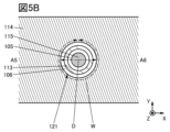
- 5A and 5B are plan views showing a configuration example of a semiconductor device.
- 6A and 6B are cross-sectional views showing a configuration example of a semiconductor device.
- FIG. 9A is a plan view showing a configuration example of a semiconductor device
- Fig. 9B and Fig. 9C are cross-sectional views showing the configuration example of a semiconductor device
- 10A to 10C are plan views showing configuration examples of a semiconductor device.
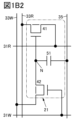
- Fig. 11A is a block diagram showing a configuration example of a semiconductor device
- Fig. 11B is a circuit diagram showing a configuration example of a memory cell.
- Fig. 12A is a plan view showing a configuration example of a semiconductor device, and Fig.
- FIG. 12B and Fig. 12C are cross-sectional views showing the configuration example of a semiconductor device.
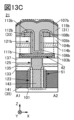
- Fig. 13A is a circuit diagram showing a configuration example of a memory cell
- Fig. 13B is a plan view showing a configuration example of a semiconductor device
- Fig. 13C and Fig. 13D are cross-sectional views showing the configuration example of a semiconductor device.
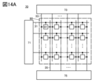
- Fig. 14A is a block diagram showing an example of the configuration of a display device
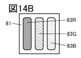
- Fig. 14B is a plan view showing an example of the configuration of a pixel
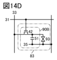
- Fig. 14C and Fig. 14D are circuit diagrams showing an example of the configuration of a sub-pixel.
- Fig. 15A is a plan view showing a configuration example of a semiconductor device
- Fig. 15A is a plan view showing a configuration example of a semiconductor device
- Fig. 15A is a plan view showing a configuration example of a semiconductor device
- Fig. 15A is a plan view showing
- FIG. 15B and Fig. 15C are cross-sectional views showing the configuration example of a semiconductor device.
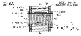
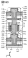
- Fig. 16A is a plan view showing a configuration example of a semiconductor device
- Fig. 16B and Fig. 16C are cross-sectional views showing the configuration example of a semiconductor device.
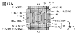
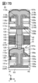
- Fig. 17A is a plan view showing a configuration example of a semiconductor device
- Fig. 17B and Fig. 17C are cross-sectional views showing the configuration example of a semiconductor device.
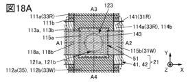
- Fig. 18A is a plan view showing a configuration example of a semiconductor device
- Fig. 18B and Fig. 18C are cross-sectional views showing the configuration example of a semiconductor device.
- Fig. 18A is a plan view showing a configuration example of a semiconductor device
- Fig. 18B and Fig. 18C are cross-sectional views showing the configuration example of a semiconductor device.
- Fig. 18A is a plan view showing a configuration example of a semiconductor device
- FIG. 19A is a plan view showing a configuration example of a semiconductor device
- Fig. 19B and Fig. 19C are cross-sectional views showing the configuration example of a semiconductor device.
- Fig. 20A is a plan view showing a configuration example of a semiconductor device
- Fig. 20B and Fig. 20C are cross-sectional views showing the configuration example of a semiconductor device.
- 21A and 21B are cross-sectional views showing a configuration example of a semiconductor device.
- 22A and 22B are cross-sectional views showing a configuration example of a semiconductor device.
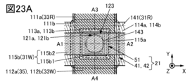
- Fig. 23A is a plan view showing a configuration example of a semiconductor device
- Fig. 23B and Fig. 23C are cross-sectional views showing the configuration example of a semiconductor device.
- Fig. 23A is a plan view showing a configuration example of a semiconductor device
- Fig. 23B and Fig. 23C are cross-sectional views showing the configuration example of a semiconductor device.
- FIG. 24A is a plan view showing a configuration example of a semiconductor device
- Fig. 24B and Fig. 24C are cross-sectional views showing the configuration example of a semiconductor device.
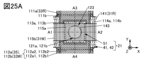
- Fig. 25A is a plan view showing a configuration example of a semiconductor device
- Fig. 25B and Fig. 25C are cross-sectional views showing the configuration example of a semiconductor device.
- Fig. 26A is a plan view showing a configuration example of a semiconductor device
- Fig. 26B and Fig. 26C are cross-sectional views showing the configuration example of a semiconductor device.
- Fig. 27A is a plan view showing a configuration example of a semiconductor device
- FIG. 27C are cross-sectional views showing the configuration example of a semiconductor device.
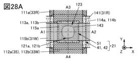
- Fig. 28A is a plan view showing a configuration example of a semiconductor device
- Fig. 28B and Fig. 28C are cross-sectional views showing the configuration example of a semiconductor device.
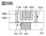
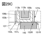
- 29A to 29D are cross-sectional views showing configuration examples of a semiconductor device.
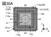
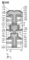
- Fig. 30A is a plan view showing a configuration example of a semiconductor device
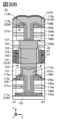
- Fig. 30B and Fig. 30C are cross-sectional views showing the configuration example of a semiconductor device.
- 31A and 31B are cross-sectional views showing a configuration example of a semiconductor device.
- 32A and 32B are cross-sectional views showing a configuration example of a semiconductor device.
- 33A and 33B are cross-sectional views showing a configuration example of a semiconductor device.
- 34A and 34B are plan views and sectional views showing an example of the configuration of a semiconductor device, respectively.
- 35A and 35B are cross-sectional views showing a configuration example of a semiconductor device.
- Fig. 36A is a plan view showing a configuration example of a semiconductor device
- Fig. 36B and Fig. 36C are cross-sectional views showing the configuration example of a semiconductor device.
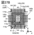
- 37A and 37B are plan views and cross-sectional views showing an example of the configuration of a semiconductor device, respectively.
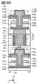
- Fig. 38A is a plan view showing a configuration example of a semiconductor device
- Fig. 39A is a plan view showing a configuration example of a semiconductor device
- Fig. 39B and Fig. 39C are cross-sectional views showing the configuration example of a semiconductor device.
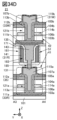
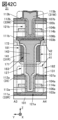
- Fig. 40A is a plan view showing a configuration example of a semiconductor device
- Fig. 40B and Fig. 40C are cross-sectional views showing the configuration example of a semiconductor device.
- Fig. 41A is a plan view showing a configuration example of a semiconductor device
- Fig. 41B and Fig. 41C are cross-sectional views showing the configuration example of a semiconductor device.
- Fig. 42A is a plan view showing a configuration example of a semiconductor device
- Fig. 42A is a plan view showing a configuration example of a semiconductor device
- Fig. 42A is a plan view showing a configuration example of a semiconductor device
- Fig. 42A is a plan view showing a configuration example of a semiconductor device
- Fig. 42A is a plan view showing a
- FIG. 42B and Fig. 42C are cross-sectional views showing the configuration example of a semiconductor device.
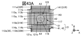
- Fig. 43A is a plan view showing a configuration example of a semiconductor device
- Fig. 43B and Fig. 43C are cross-sectional views showing the configuration example of a semiconductor device.
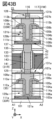
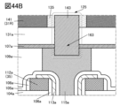
- 44A and 44B are cross-sectional views showing a configuration example of a semiconductor device.
- Fig. 45A is a plan view showing a configuration example of a semiconductor device
- Fig. 45B and Fig. 45C are cross-sectional views showing the configuration example of a semiconductor device.
- Fig. 46A is a plan view showing a configuration example of a semiconductor device
- FIG. 46C are cross-sectional views showing the configuration example of a semiconductor device.
- Fig. 47A is a plan view showing a configuration example of a semiconductor device
- Fig. 47B and Fig. 47C are cross-sectional views showing the configuration example of a semiconductor device.
- Fig. 48A is a plan view showing a configuration example of a semiconductor device
- Fig. 48B and Fig. 48C are cross-sectional views showing the configuration example of a semiconductor device.
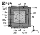
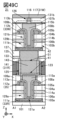
- 49A and 49B are plan views and 49C and 49D are cross-sectional views showing an example of the configuration of a semiconductor device.
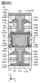
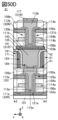
- 50A and 50B are plan views and 50C and 50D are cross-sectional views showing an example of the configuration of a semiconductor device.
- 51A is a plan view showing a configuration example of a semiconductor device
- Fig. 51B and Fig. 51C are cross-sectional views showing the configuration example of a semiconductor device.
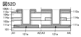
- 52A to 52D are cross-sectional views showing an example of a method for manufacturing a semiconductor device.
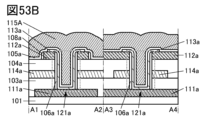
- 53A to 53C are cross-sectional views showing an example of a method for manufacturing a semiconductor device.
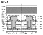
- 54A and 54B are cross-sectional views showing an example of a method for manufacturing a semiconductor device.
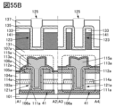
- 55A and 55B are cross-sectional views illustrating an example of a method for manufacturing a semiconductor device.
- 56A and 56B are cross-sectional views illustrating an example of a method for manufacturing a semiconductor device.
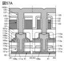
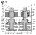
- 57A and 57B are cross-sectional views illustrating an example of a method for manufacturing a semiconductor device.
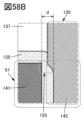
- 58A to 58C are cross-sectional views showing configuration examples of a semiconductor device.
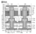
- 59A and 59B are cross-sectional views illustrating an example of a method for manufacturing a semiconductor device.
- FIG. 60 is a cross-sectional view showing an example of a method for manufacturing a semiconductor device.
- 61A and 61B are cross-sectional views showing an example of a method for manufacturing a semiconductor device.
- 62A and 62B are cross-sectional views showing an example of a method for manufacturing a semiconductor device.
- 63A and 63B are cross-sectional views showing an example of a method for manufacturing a semiconductor device.
- 64A and 64B are cross-sectional views showing an example of a method for manufacturing a semiconductor device.
- 65A and 65B are cross-sectional views showing an example of a method for manufacturing a semiconductor device.
- 66A and 66B are cross-sectional views showing an example of a method for manufacturing a semiconductor device.
- 67A and 67B are cross-sectional views showing an example of a method for manufacturing a semiconductor device.
- 68A and 68B are cross-sectional views showing an example of a method for manufacturing a semiconductor device.
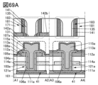
- 69A and 69B are cross-sectional views showing an example of a method for manufacturing a semiconductor device.
- 70A and 70B are cross-sectional views illustrating an example of a method for manufacturing a semiconductor device.
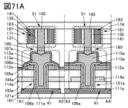
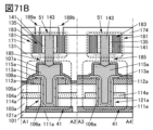
- 71A and 71B are cross-sectional views showing an example of a method for manufacturing a semiconductor device.
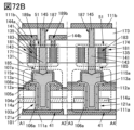
- 72A and 72B are cross-sectional views illustrating an example of a method for manufacturing a semiconductor device.
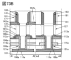
- 73A and 73B are cross-sectional views showing an example of a method for manufacturing a semiconductor device.
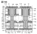
- 74A and 74B are cross-sectional views showing an example of a method for manufacturing a semiconductor device.
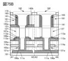
- 75A and 75B are cross-sectional views illustrating an example of a method for manufacturing a semiconductor device.
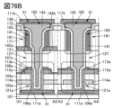
- 76A and 76B are cross-sectional views showing an example of a method for manufacturing a semiconductor device.
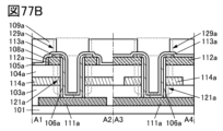
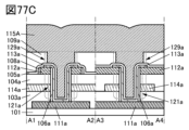
- 77A to 77C are cross-sectional views showing an example of a method for manufacturing a semiconductor device.
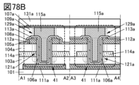
- FIG. 78A to 78C are cross-sectional views showing an example of a method for manufacturing a semiconductor device.
- FIG. 79 is a cross-sectional view showing an example of a method for manufacturing a semiconductor device.
- 80A and 80B are cross-sectional views illustrating an example of a method for manufacturing a semiconductor device.
- 81A and 81B are cross-sectional views showing an example of a method for manufacturing a semiconductor device.
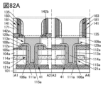
- 82A and 82B are cross-sectional views showing an example of a method for manufacturing a semiconductor device.
- FIG. 83 is a perspective view showing a configuration example of a semiconductor device.
- FIG. 84 is a cross-sectional view showing a configuration example of a semiconductor device.
- FIG. 85 is a cross-sectional view showing a configuration example of a semiconductor device.
- 86A and 86B are diagrams showing an example of an electronic component.
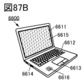
- 87A and 87B are diagrams showing an example of an electronic device, and
- Fig. 87C to Fig. 87E are diagrams showing an example of a mainframe computer.
- FIG. 88 is a diagram showing an example of space equipment.
- FIG. 89 is a diagram illustrating an example of a storage system applicable to a data center.
- the position, size, range, etc. of each component shown in the drawings may not represent the actual position, size, range, etc.
- the disclosed invention is not necessarily limited to the position, size, range, etc. disclosed in the drawings.
- a layer or resist mask may be unintentionally reduced by a process such as etching, but this may not be reflected in the drawings for ease of understanding.
- ordinal numbers “first” and “second” are used for convenience and do not limit the number of components or the order of the components (e.g., the order of processes or the order of stacking).
- an ordinal number attached to a component in one place in this specification may not match an ordinal number attached to the same component in another place in this specification or in the claims.
- a transistor is a type of semiconductor element that can perform functions such as amplifying current or voltage and switching operations that control conduction or non-conduction.
- transistor includes an IGFET (Insulated Gate Field Effect Transistor) and a thin film transistor (TFT).
- a transistor is an element having at least three terminals including a gate, a drain, and a source.
- a region also called a channel formation region in which a channel is formed between the drain (drain terminal, drain region, or drain electrode) and the source (source terminal, source region, or source electrode) is included, and a current can flow between the source and drain through the channel formation region.
- a channel formation region refers to a region through which a current mainly flows.
- source and drain may be interchanged when transistors of different polarity are used, or when the direction of current changes during circuit operation. For this reason, in this specification, the terms “source” and “drain” may be used interchangeably.
- the impurity of a semiconductor refers to, for example, anything other than the main component constituting the semiconductor.
- an element with a concentration of less than 0.1 atomic % can be said to be an impurity.
- the defect state density of the semiconductor may be increased or the crystallinity may be reduced.
- the semiconductor is an oxide semiconductor
- examples of the impurity that changes the characteristics of the semiconductor include, for example, Group 1 elements, Group 2 elements, Group 13 elements, Group 14 elements, Group 15 elements, and transition metals other than the main components of the oxide semiconductor.
- Specific examples of the impurity include, for example, hydrogen, lithium, sodium, silicon, boron, phosphorus, carbon, and nitrogen.
- water may also function as an impurity.
- oxygen vacancies also referred to as V O
- V O oxygen vacancies
- an oxynitride refers to a material whose composition contains more oxygen than nitrogen.
- An oxynitride refers to a material whose composition contains more nitrogen than oxygen.
- SIMS secondary ion mass spectrometry
- XPS X-ray photoelectron spectroscopy
- parallel refers to a state in which two straight lines are arranged at an angle of -10 degrees or more and 10 degrees or less. Therefore, it also includes cases where the angle is -5 degrees or more and 5 degrees or less.
- approximately parallel refers to a state in which two straight lines are arranged at an angle of -30 degrees or more and 30 degrees or less.
- Perfect refers to a state in which two straight lines are arranged at an angle of 80 degrees or more and 100 degrees or less. Therefore, it also includes cases where the angle is 85 degrees or more and 95 degrees or less.
- approximately perpendicular refers to a state in which two straight lines are arranged at an angle of 60 degrees or more and 120 degrees or less.
- electrically connected includes a connection via "something that has some kind of electrical action.”
- something that has some kind of electrical action is not particularly limited as long as it allows the transmission and reception of electrical signals between the connected objects.
- something that has some kind of electrical action includes electrodes or wiring, as well as switching elements such as transistors, resistive elements, coils, capacitance, and other elements with various functions.
- a tapered shape refers to a shape in which at least a portion of the side of the structure is inclined with respect to the substrate surface or the surface to be formed.
- the side of the structure, the substrate surface, and the surface to be formed do not necessarily need to be completely flat, and may be approximately planar with a slight curvature, or approximately planar with fine irregularities.
- A covers B
- at least a part of A covers B. Therefore, for example, it can be rephrased as saying that A has an area that covers B.
- One aspect of the present invention relates to a memory device having a memory section in which memory cells are arranged in a matrix.
- the memory cell has a first transistor, a second transistor, and a capacitor.
- the first transistor may be a transistor in which a semiconductor layer is provided inside an opening formed in an interlayer insulating layer on a substrate.
- a lower electrode provided under the opening is used as one of the source electrode and drain electrode of the first transistor.
- an interlayer insulating layer is provided on the lower electrode, and an opening is provided in the interlayer insulating layer so as to reach the lower electrode.
- a semiconductor layer is provided so as to have a region in contact with the lower electrode inside the opening.
- an upper electrode provided on the interlayer insulating layer is used as the other of the source electrode and drain electrode of the first transistor.
- the upper electrode may have an opening that overlaps with the above opening.
- the channel length direction of the first transistor can be set to the direction along the side surface of the interlayer insulating layer in the opening. Therefore, the channel length is not affected by the performance of the exposure device used to manufacture the first transistor. Therefore, the channel length can be made smaller than the limit resolution of the exposure device.
- the transistor having the above configuration can occupy a smaller area in a planar view than, for example, a planar transistor. Therefore, the memory cell can be miniaturized and highly integrated. Therefore, one aspect of the present invention can provide a memory device that can be miniaturized and highly integrated.
- the second transistor is provided on the first transistor.
- the second transistor can have the same configuration as the first transistor.
- a first conductive layer is provided between a gate electrode of a first transistor and a lower electrode of a second transistor.
- the gate electrode of the first transistor and the lower electrode of the second transistor are electrically connected by the first conductive layer.
- a dielectric layer is provided so as to have a region in contact with a side surface of the first conductive layer
- a second conductive layer is provided so as to cover at least a part of the side surface of the first conductive layer via the dielectric layer.
- the second conductive layer is provided so as to have a region in contact with a side surface of the dielectric layer opposite to the side surface in contact with the first conductive layer.
- a capacitance having the first conductive layer, the dielectric layer, and the second conductive layer can be provided between the first transistor and the second transistor.
- the first transistor, the capacitor, and the second transistor are stacked in this order.
- the first and second transistors are transistors in which a semiconductor layer, a gate insulating layer, and a gate electrode are provided inside an opening formed in an interlayer insulating layer.
- the first and second transistors are transistors in which one of a source electrode and a drain electrode is provided under the opening and the other of a source electrode and a drain electrode is provided on the interlayer insulating layer.
- a planar view refers to a view from the normal direction of the surface on which the component is formed or the surface of the support (e.g., substrate) on which the component is formed.
- a planar view can sometimes be rephrased as a top view or a bottom view.
- the first transistor and the second transistor each have a backgate electrode.
- the upper and lower surfaces of the backgate electrode are covered with an interlayer insulating layer, and the backgate electrode has an opening.
- the opening overlaps with the opening of the interlayer insulating layer.
- the interlayer insulating layer can cover the upper and lower surfaces of the backgate electrode, as well as the side surface of the backgate electrode opposite the opening. Note that one of the first transistor and the second transistor does not necessarily have a backgate electrode.
- a gate insulating layer different from the above gate insulating layer is provided between the back gate electrode and the semiconductor layer.
- This gate insulating layer is called a back gate insulating layer.
- the back gate insulating layer has a region located inside the opening of the back gate electrode. For example, after forming an interlayer insulating layer having an opening, a back gate electrode, and an upper electrode, an insulating film is formed to cover the opening. Then, anisotropic etching is performed on the insulating film until at least a part of the upper surface of the lower electrode and the upper surface of the upper electrode are exposed, thereby forming a back gate insulating layer inside the opening.
- the semiconductor layer is provided so as to cover the back gate insulating layer.
- the back gate electrode and the semiconductor layer have regions that face each other with the back gate insulating layer sandwiched between them inside the opening of the back gate electrode.
- a gate insulating layer is provided on the semiconductor layer, and a gate electrode is provided on the gate insulating layer.
- the gate electrode and the back gate electrode have regions that face each other with the gate insulating layer, the semiconductor layer, and the back gate insulating layer sandwiched between them, the region being located inside the opening of the back gate electrode.
- the threshold voltage of the transistor can be changed.
- the variation in electrical characteristics that may occur between multiple transistors can be reduced. As a result, for example, a highly reliable semiconductor device can be provided.
- ⁇ Configuration Example 1 of Semiconductor Device> 1A is a block diagram showing a configuration example of a semiconductor device 10.
- the semiconductor device 10 can be a memory device.
- the semiconductor device 10 has a memory unit 20, a word line driving circuit 11, a bit line driving circuit 13, and a power supply circuit 15.
- the memory unit 20 has a plurality of memory cells 21 arranged in a matrix.
- the power supply circuit 15 may be provided outside the semiconductor device 10.
- the word line driving circuit 11 is electrically connected to the memory cells 21 via the wiring 31.
- the wiring 31 extends, for example, in the row direction of the matrix.
- the wiring 31 functions as a word line.
- the wiring 31 includes wiring 31W and wiring 31R.
- the bit line driving circuit 13 is electrically connected to the memory cells 21 via the wiring 33.
- the wiring 33 extends, for example, in the column direction of the matrix.
- the wiring 33 functions as a bit line.
- the wiring 33 includes wiring 33W and wiring 33R.
- the direction in which the wiring 31 functioning as the word line extends is the X direction
- the direction in which the wiring 33 functioning as the bit line extends is the Y direction.
- the wiring 31 extends in the row direction of the matrix
- the wiring 33 extends in the column direction of the matrix. Therefore, the X direction can be the row direction
- the Y direction can be the column direction.
- the X direction and the Y direction can be directions that intersect with each other, specifically, directions that are perpendicular to each other.
- the direction that intersects with both the X direction and the Y direction specifically, the direction that is perpendicular to both the X direction and the Y direction, can be the Z direction.
- the definitions of the X direction, the Y direction, and the Z direction are shown on the coordinate axis, but the definitions may be the same as those in FIG. 1A, or may be different. Also, in FIG. 1A, the X direction, the Y direction, and the Z direction are shown by arrows, but the forward direction and the reverse direction are not distinguished unless explicitly stated. This is also true in the following drawings.
- the power supply circuit 15 is electrically connected to the memory cells 21 via wiring 35.
- FIG. 1A shows an example in which the wiring 35 extends in the column direction of the matrix.
- the wiring 35 functions as a power supply line.
- wiring 31, wiring 33, and wiring 35 are shown as straight lines, but one straight line is not necessarily one wiring, and multiple wirings may be represented by one straight line. In the block diagrams and circuit diagrams that follow, multiple wirings may also be represented by one straight line. Furthermore, multiple wirings other than wiring 31, wiring 33, and wiring 35 may also be represented by one straight line.
- the word line driver circuit 11 has a function of selecting the memory cell 21 to which data is written, for each row.
- the word line driver circuit 11 also has a function of selecting the memory cell 21 from which data is read, specifically the memory cell 21 that outputs data to the wiring 33, for each row.
- the word line driver circuit 11 has a function of selecting the memory cell 21 to which data is written or the memory cell 21 from which data is read, by supplying a signal to the wiring 31.
- the word line driver circuit 11 has a function of selecting the memory cell 21 to which data is written, by supplying a signal to the wiring 31W.
- a pulse signal refers to a signal whose potential changes over time.
- the bit line driver circuit 13 has a function of writing data to the memory cell 21 selected by the word line driver circuit 11 via the wiring 33.
- the bit line driver circuit 13 also has a function of amplifying the data output by the memory cell 21 to the wiring 33 and outputting it, for example, to the outside of the semiconductor device 10, thereby reading out the data held in the memory cell 21. Furthermore, the bit line driver circuit 13 has a function of precharging the wiring 33 before reading out the data from the memory cell 21.
- the bit line driver circuit 13 has a function of writing data via the wiring 33W to the memory cell 21 selected by the word line driver circuit 11 using a write signal.
- the bit line driver circuit 13 also has a function of reading the data held in the memory cell 21 by amplifying the data output by the memory cell 21 to the wiring 33R and outputting it, for example, to the outside of the semiconductor device 10.
- the bit line driver circuit 13 has a function of precharging the wiring 33R before reading data from the memory cell 21.
- the wiring 33W is also called the write bit line
- the wiring 33R is also called the read bit line.
- the bit line driving circuit 13 has a function of writing data to the memory cell 21 via the wiring 33W.
- the bit line driving circuit 13 also has a function of reading the data via the wiring 33R.
- the power supply circuit 15 has a function of supplying a power supply potential to the wiring 35, specifically, a function of supplying a constant potential to the wiring 35.
- the power supply circuit 15 has a function of generating, for example, a high potential or a low potential and supplying it to the wiring 35. Note that the power supply circuit 15 may have a function of supplying a power supply potential to one or both of the word line driver circuit 11 and the bit line driver circuit 13.
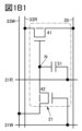
- FIG. 1B1 is a circuit diagram showing an example configuration of a memory cell 21.
- the memory cell 21 has a transistor 41, a transistor 42, and a capacitor 51.
- One of the source and drain of transistor 41 is electrically connected to wiring 33R.
- the other of the source and drain of transistor 41 is electrically connected to wiring 35.
- the gate of transistor 41 is electrically connected to one of the source and drain of transistor 42.
- One of the source and drain of transistor 42 is electrically connected to one electrode of capacitance 51.
- the other of the source and drain of transistor 42 is electrically connected to wiring 33W.
- the gate of transistor 42 is electrically connected to wiring 31W.
- the other electrode of capacitance 51 is electrically connected to wiring 31R.
- node N a node to which the gate of transistor 41, one of the source and drain of transistor 42, and one electrode of capacitance 51 are electrically connected.
- Transistor 41 and transistor 42 each have a back gate in addition to a gate.
- the gate can be referred to as a first gate
- the back gate can be referred to as a second gate.
- the first gate can also be referred to as a front gate.
- gate and backgate can be used interchangeably. Therefore, in this specification, the terms “gate” and “backgate” can be used interchangeably. Note that the gate and backgate of a transistor can be appropriately rephrased as a gate electrode and a backgate electrode, etc., depending on the situation.
- the transistor 42 has a function as a switch.
- the transistor 42 when the transistor 42 is an n-channel transistor, the transistor 42 can be turned on by setting the potential of the wiring 31W to a high potential.
- the transistor 42 can be turned off by setting the potential of the wiring 31W to a low potential.
- the transistor 42 has a function of controlling the conductive state and non-conductive state between the wiring 33W and the node N based on the potential of the wiring 31W. By setting the transistor 42 to an on state, data is written to the memory cell 21 through the wiring 33W, and the written data is held by setting the transistor 42 to an off state.
- the transistor 42 by setting the transistor 42 to an on state, charge corresponding to the data is accumulated in the node N, and the charge of the node N is held by setting the transistor 42 to an off state.
- the potential of the wiring 31R is set to, for example, a low potential.
- transistors 41 and 42 are described as n-channel transistors, but the following description can be applied even if one or both of transistors 41 and 42 are p-channel transistors by appropriately reversing the magnitude relationship of the potentials.
- the transistor 41 has a function of controlling the reading of data stored in the memory cell 21. Below, a method of reading data stored in the memory cell 21 will be described.
- the memory cell 21 stores binary data having a value of "0" or “1” as the potential of the node N, and "1" is represented by a potential higher than "0".
- wiring 33R is precharged to a high potential. Also, the potential of wiring 35 is set to a low potential. Furthermore, the potential of wiring 31R is set to a low potential. In this state, regardless of whether the data stored in memory cell 21 is "0" or "1", the difference between the gate potential and source potential of transistor 41, specifically the difference between the potential of node N and wiring 35, is set to be lower than the threshold voltage of transistor 41, for example.
- the potential of the wiring 31R is set to a high potential. This causes the potential of the node N to rise due to capacitive coupling.
- the difference between the gate potential and the source potential of the transistor 41 is assumed to be lower than the threshold voltage of the transistor 41.
- the difference between the gate potential and the source potential of the transistor 41 is assumed to exceed the threshold voltage of the transistor 41 by setting the potential of the wiring 31R to a high potential.
- the bit line driving circuit 13 can read out the data held in the memory cell 21 from the current flowing through the wiring 33R or the potential of the wiring 33R.
- the potential of the wiring 31R is high, the difference between the gate potential and the source potential of the transistor 41 may exceed the threshold voltage of the transistor 41, regardless of whether the data stored in the memory cell 21 is "0" or "1.” Even in this case, the bit line driving circuit 13 can read the data stored in the memory cell 21, for example, by reading the magnitude of the current flowing through the wiring 33R.
- OS transistors for transistor 41 and transistor 42.
- metal oxides contained in the channel formation region of an OS transistor include indium oxide, gallium oxide, and zinc oxide.
- the configuration of the memory cell 21 in which the transistors 41 and 42 are OS transistors is also called NOSRAM (registered trademark) (Nonvolatile Oxide Semiconductor Random Access Memory).
- Transistors other than OS transistors may be used as transistors 41 and 42.
- transistors having silicon in the channel formation region also called Si transistors
- silicon for example, single crystal silicon, amorphous silicon (sometimes called hydrogenated amorphous silicon), microcrystalline silicon, or polycrystalline silicon (including low-temperature polycrystalline silicon) can be used.
- OS transistors have a significantly small leakage current between the source and drain in an off state (also referred to as off-state current). Therefore, by using an OS transistor as the transistor 42, the charge stored in the node N can be held for a long period of time. Since data written to the memory cell 21 can be held for a long period of time, the frequency of refresh operations (rewriting data to the memory cell 21) can be reduced. Therefore, the power consumption of the semiconductor device 10 can be reduced.
- Si transistors may have a larger on-state current than OS transistors. In this case, by using a Si transistor as transistor 41, data stored in memory cell 21 can be read at high speed.
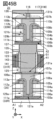
- Figure 2A is a plan view showing a configuration example of a portion of a semiconductor device 10, which is a semiconductor device according to one embodiment of the present invention.
- Figure 2A includes a configuration example of a memory cell 21 shown in Figure 1B1.
- Figure 2A some elements such as an insulating layer are omitted for clarity. Some elements are also omitted in the plan views shown below.
- Figure 2B is a cross-sectional view taken along dashed line A1-A2 in Figure 2A.
- Figure 2C is a cross-sectional view taken along dashed line A3-A4 in Figure 2A.
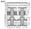
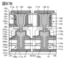
- a semiconductor device has an insulating layer 101 on a substrate (not shown) and a memory cell 21 on the insulating layer 101.
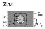
- the memory cell 21 has a transistor 41, a capacitance 51 on the transistor 41, and a transistor 42 on the capacitance 51.
- the memory cell 21 has a transistor 42, a capacitance 51 below the transistor 42, and a transistor 41 below the capacitance 51.
- a semiconductor device of one embodiment of the present invention has an insulating layer 103a on insulating layer 101, an insulating layer 104a on insulating layer 103a, an insulating layer 107a on transistor 41 and on insulating layer 104a, an insulating layer 131 on insulating layer 107a, a capacitor 51 on transistor 41 and on insulating layer 131, an insulating layer 133 on capacitor 51 and on insulating layer 131, an insulating layer 137 on insulating layer 131 and on insulating layer 133, a transistor 42 on capacitor 51 and on insulating layer 137, an insulating layer 103b, an insulating layer 104b on insulating layer 103b, and an insulating layer 107b on transistor 42 and on insulating layer 104b.
- insulating layer 101, insulating layer 103a, insulating layer 104a, insulating layer 131, insulating layer 137, insulating layer 103b, and insulating layer 104b function as interlayer insulating layers. It is preferable that the layers that function as interlayer insulating layers, including these insulating layers, are planarized. Note that the layers that function as interlayer insulating layers do not have to be planarized.
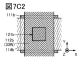
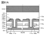
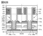
- Transistor 41 has conductive layer 111a, conductive layer 114a, conductive layer 112a, insulating layer 106a, semiconductor layer 113a, insulating layer 105a, and conductive layer 115a.
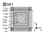
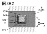
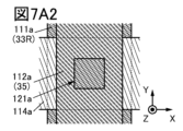
- FIG. 3A1 shows a plan view of transistor 41 excerpted from FIG. 2A.
- FIG. 3A2 shows a plan view of FIG. 3A1 with conductive layer 115a and semiconductor layer 113a omitted.
- At least a part of the conductive layer 111a functions as one of the source electrode and drain electrode of the transistor 41. At least a part of the conductive layer 111a functions as the wiring 33R. At least a part of the conductive layer 112a functions as the other of the source electrode and drain electrode of the transistor 41. At least a part of the conductive layer 112a functions as the wiring 35. At least a part of the insulating layer 105a functions as the first gate insulating layer of the transistor 41. At least a part of the conductive layer 115a functions as the first gate electrode (also called the front gate electrode) of the transistor 41. At least a part of the insulating layer 106a functions as the second gate insulating layer of the transistor 41.
- At least a part of the conductive layer 114a functions as the second gate electrode (also called the back gate electrode) of the transistor 41.
- Figures 2A and 2B show an example in which the conductive layer 114a has a region extending in the X direction.
- Figures 2A and 2C, etc. an example is shown in which conductive layer 111a, at least a portion of which functions as wiring 33R, and conductive layer 112a, at least a portion of which functions as wiring 35, have regions that extend in the Y direction.
- a conductive layer 111a is provided on the insulating layer 101, an insulating layer 103a is provided on the insulating layer 101 and on the conductive layer 111a, a conductive layer 114a is provided on the insulating layer 103a, an insulating layer 104a is provided on the insulating layer 103a and on the conductive layer 114a, and a conductive layer 112a is provided on the insulating layer 104a. That is, the conductive layer 111a, the insulating layer 103a, the conductive layer 114a, the insulating layer 104a, and the conductive layer 112a are provided in different layers.
- the insulating layer 103a covers at least a portion of the upper surface and side surface of the conductive layer 111a.
- the insulating layer 104a covers at least a portion of the upper surface and side surface of the conductive layer 114a.
- the conductive layer 111a and the conductive layer 114a can have an overlapping region with the insulating layer 103a interposed therebetween.
- the conductive layer 114a and the conductive layer 112a can have an overlapping region with the insulating layer 104a interposed therebetween.
- the insulating layer 103a, the conductive layer 114a, and the insulating layer 104a are provided on the conductive layer 111a.
- the conductive layer 112a is provided on the insulating layer 103a, the conductive layer 114a, and the insulating layer 104a.
- the conductive layer 111a having a region located under the insulating layer 103a can be referred to as the lower electrode of the transistor 41.
- the conductive layer 112a having a region located on the insulating layer 104a can be referred to as the upper electrode of the transistor 41.
- the insulating layer 103a, the conductive layer 114a, the insulating layer 104a, and the conductive layer 112a have an opening 121a that reaches the conductive layer 111a.
- Figures 2A, 3A1, and 3A2 show an example in which the shape of the opening 121a is circular in a planar view. By making the shape of the opening 121a circular in a planar view, the processing accuracy when forming the opening 121a can be improved, and the opening 121a can be formed with a fine size. Note that in this specification, a circle is not limited to a perfect circle. Furthermore, the shape of the opening 121a in a planar view may be, for example, an ellipse.
- the bottom of the opening 121a includes the top surface of the conductive layer 111a.
- the sidewalls of the opening 121a include the side surface of the insulating layer 103a, the side surface of the conductive layer 114a, the side surface of the insulating layer 104a, and the side surface of the conductive layer 112a.
- the opening 121a includes an opening in the insulating layer 103a, an opening in the conductive layer 114a, an opening in the insulating layer 104a, and an opening in the conductive layer 112a.
- the openings in the insulating layer 103a, the openings in the conductive layer 114a, the openings in the insulating layer 104a, and the openings in the conductive layer 112a that are provided in the area overlapping with the conductive layer 111a are each part of the opening 121a.
- the shape and size of the opening 121a in a planar view may differ depending on each layer.
- the shape of the opening 121a is circular in plan view, the openings in each layer may or may not be concentric.
- insulating layer 103a and insulating layer 104a function as interlayer insulating layers. Therefore, as shown in FIG. 2C, the upper surface, lower surface, and side surface opposite opening 121a of conductive layer 114a can be said to be covered with an interlayer insulating layer.
- FIGS. 2A and 2B show an example in which the side end of the conductive layer 111a is located outside the side end of the conductive layer 112a opposite the opening 121a in the X direction, i.e., the side end of the conductive layer 112a opposite the opening 121a overlaps with the conductive layer 111a, and the side end of the conductive layer 111a does not overlap with the conductive layer 112a, but this is not a limitation of one embodiment of the present invention.
- the side end of the conductive layer 111a may be located inside the side end of the conductive layer 112a opposite the opening 121a.
- the semiconductor layer 113a covers the opening 121a and has a region located inside the opening 121a.
- the semiconductor layer 113a has a recess at a position overlapping the opening 121a.
- the semiconductor layer 113a can have a region in contact with the upper surface of the conductive layer 112a and a region in contact with the upper surface of the conductive layer 111a. Note that the conductive layer 112a does not need to have an opening 121a formed as long as it has a region in contact with the semiconductor layer 113a.
- FIG. 2A to 2C show an example in which the side end of the semiconductor layer 113a is located inside the side end of the conductive layer 112a opposite the opening 121a, i.e., the entire semiconductor layer 113a overlaps with either the conductive layer 112a or the opening 121a. Also, FIG. 2A to 2C show an example in which the side end of the semiconductor layer 113a is located inside the side end of the conductive layer 111a, i.e., the entire semiconductor layer 113a overlaps with the conductive layer 111a.
- the semiconductor layer 113a is shown to have a single-layer structure in FIG. 2B and FIG. 2C, one embodiment of the present invention is not limited to this.
- the semiconductor layer 113a may have a stacked structure of two or more layers.
- the insulating layer 106a has a region located at least between the conductive layer 114a and the semiconductor layer 113a inside the opening 121a.
- the conductive layer 114a and the semiconductor layer 113a have regions that face each other across the insulating layer 106a located inside the opening 121a.
- 2B and 2C show an example in which the insulating layer 106a has, inside the opening 121a, a region located between the insulating layer 103a and the semiconductor layer 113a, a region located between the conductive layer 114a and the semiconductor layer 113a, a region located between the insulating layer 104a and the semiconductor layer 113a, and a region located between the conductive layer 112a and the semiconductor layer 113a.
- 2B and 2C show an example in which the insulating layer 106a has a region in contact with the upper surface of the conductive layer 111a, the side of the insulating layer 103a, the side of the conductive layer 114a, the side of the insulating layer 104a, the side of the conductive layer 112a, and the recess side of the semiconductor layer 113a.
- FIG. 2B and 2C show an example in which a curved portion is provided between the upper surface and the side surface of the insulating layer 106a. Also, FIG. 2B and FIG. 2C show an example in which the height of the top of the insulating layer 106a coincides with or approximately coincides with the height of the upper surface of the conductive layer 112a.
- the curved portion in an element in which a curved portion is provided between an upper surface and a side surface, the curved portion may be included in the upper surface. Also, the curved portion may be included in the side surface.
- the top of a layer refers to the part of the layer that is the highest above a reference surface.
- the reference surface is preferably a flat surface.
- the reference surface can be, for example, the substrate surface or the top surface of the insulating layer 101.
- the same height refers to a configuration in which the heights from a reference plane are equal when viewed in cross section.
- the insulating layer 106a can be formed by forming an insulating film to cover the opening 121a, and then performing anisotropic etching on the insulating film until the upper surface of the conductive layer 111a and at least a part of the upper surface of the conductive layer 112a are exposed.
- the top of the insulating layer 106a can be aligned or approximately aligned with the upper surface of the conductive layer 112a. Alternatively, the top of the insulating layer 106a can be lower than the upper surface of the conductive layer 112a.
- the insulating layer 106a When the insulating layer 106a is formed using anisotropic etching, the insulating layer 106a can be formed without performing pattern formation using, for example, a lithography method. Therefore, the insulating layer 106a can be formed without considering the accuracy of mask alignment. Therefore, even if the opening 121a is miniaturized, it is possible to prevent the insulating layer 106a from not being formed inside the opening 121a. Therefore, since the opening 121a can be miniaturized, the memory cell 21 can be a memory cell that occupies a small area in a planar view. Therefore, the memory cell 21 can be a miniaturized and highly integrated memory cell. As described above, a semiconductor device that can be miniaturized and highly integrated can be provided.
- the insulating layer 106a may be formed using a lithography method.
- the insulating layer 108a may be provided so as to contact at least a portion of the side of the conductive layer 112a, specifically the side opposite the opening 121a.
- the insulating layer 108a may be formed due to the formation process of the insulating layer 106a.
- the insulating layer 108a is formed as a residue when the insulating layer 106a is formed.
- Figures 2B and 2C show an example in which a curved portion is provided between the upper surface and the side of the insulating layer 108a.
- Figures 2B and 2C show an example in which the height of the top of the insulating layer 108a matches or roughly matches the height of the upper surface of the conductive layer 112a.
- one or both of a part of the conductive layer 111a and a part of the conductive layer 112a may be processed.
- a recess may be formed in the conductive layer 111a in the region overlapping with the opening 121a.
- the thickness of the conductive layer 112a may be reduced. Specifically, the thickness of the conductive layer 112a after the insulating layer 106a is formed may be thinner than the thickness of the conductive layer 112a before the insulating layer 106a is formed.
- the insulating layer 105a at least a portion of which functions as the first gate insulating layer of the transistor 41, is provided to cover the semiconductor layer 113a, the conductive layer 112a, and the insulating layer 108a.
- the insulating layer 105a has a region located inside the opening 121a.
- the insulating layer 105a is provided on the semiconductor layer 113a, the conductive layer 112a, the insulating layer 108a, and the insulating layer 104a.
- the insulating layer 105a can have a shape that follows the shapes of the upper and side surfaces of the semiconductor layer 113a, the upper surface of the conductive layer 112a, the upper and side surfaces of the insulating layer 108a, and the upper surface of the insulating layer 104a. As a result, the insulating layer 105a has a recess at a position that overlaps with the opening 121a.
- the insulating layer 105a can have a region in contact with the top surface of the semiconductor layer 113a, a region in contact with the side surface of the semiconductor layer 113a, a region in contact with the top surface of the conductive layer 112a, a region in contact with the insulating layer 108a, and a region in contact with the top surface of the insulating layer 104a.
- the conductive layer 115a at least a portion of which functions as the first gate electrode of the transistor 41, is provided on the insulating layer 105a and can have a region in contact with the upper surface of the insulating layer 105a and the side surface of the recess.
- the conductive layer 115a also has a region located inside the opening 121a.
- the conductive layer 115a and the semiconductor layer 113a have a region that faces each other inside the opening 121a with the insulating layer 105a sandwiched between them.
- the conductive layer 114a and the conductive layer 115a have a region that faces each other with the insulating layer 106a, the semiconductor layer 113a, and the insulating layer 105a sandwiched between them, which are located inside the opening 121a.
- the semiconductor layer 113a can be configured to cover the side and bottom surface of the conductive layer 115a via the insulating layer 105a.
- the insulating layer 105a can have a region in contact with the side surface of the semiconductor layer 113a, a region in contact with the upper surface of the recess of the semiconductor layer 113a, a region in contact with the side surface of the conductive layer 115a, and a region in contact with the bottom surface of the conductive layer 115a.
- the transistor 41 shown in FIG. 2B and FIG. 2C is a transistor in which a semiconductor layer, a first gate insulating layer, and a first gate electrode are provided inside an opening formed in an interlayer insulating layer.
- 3A1 show an example in which the entire opening 121a has an area overlapping with the conductive layer 111a, the semiconductor layer 113a, and the conductive layer 115a, but a part of the opening 121a does not have to overlap with at least one of the conductive layer 111a, the semiconductor layer 113a, and the conductive layer 115a.
- the source electrode and the drain electrode are located at different heights. Therefore, the current flowing through the semiconductor layer flows in the height direction. In other words, it can be said that the channel length direction has a height (vertical) component. Therefore, the transistor can be called a VFET (Vertical Field Effect Transistor), a vertical transistor, or a vertical channel transistor.
- VFET Vertical Field Effect Transistor
- the transistor 41 shown in FIG. 2B and FIG. 2C is a transistor in which a conductive layer 114a, at least a part of which functions as a second gate electrode, is provided between an insulating layer 103a and an insulating layer 104a, which function as interlayer insulating layers.
- the first gate electrode and the second gate electrode are provided to sandwich at least a part of the channel formation region of the transistor 41.
- a potential to the conductive layer 114a it is possible to control, for example, the threshold voltage of the transistor 41.
- the conductive layer 115a and the conductive layer 114a have a function of preventing an electric field generated outside the transistor 41 from acting on the channel formation region of the semiconductor layer 113a, for example, an electric field shielding function against static electricity. This can reduce the variation in electrical characteristics that may occur between multiple transistors 41. In addition, deterioration of the electrical characteristics of the transistor 41 due to a GBTS (Gate Bias Temperature Stress) test is suppressed. For example, since the transistor 41 has the conductive layer 114a, it is possible to suppress the variation in the threshold voltage before and after the GBTS test. As a result, a highly reliable semiconductor device can be provided.
- GBTS Gate Bias Temperature Stress
- GBTS testing is a type of accelerated testing that can quickly evaluate changes in transistor characteristics (aging) that occur over a long period of use.
- the amount of change in the threshold voltage of a transistor before and after GBTS testing is an important indicator for investigating reliability. The smaller the amount of change in threshold voltage before and after GBTS testing, the more reliable the transistor is.
- GBTS testing includes PBTS (Positive Bias Temperature Stress) testing, which applies a positive potential (positive bias) to the gate relative to the source potential and drain potential and holds the gate at high temperature.
- GBTS testing also includes NBTS (Negative Bias Temperature Stress) testing, which applies a negative potential (negative bias) to the gate and holds the gate at high temperature.
- the distance between the conductive layer 115a and the conductive layer 112a outside the opening 121a is shorter than the distance between the conductive layer 115a and the conductive layer 111a outside the opening 121a. Therefore, the parasitic capacitance formed by the conductive layer 115a and the conductive layer 112a is larger than the parasitic capacitance formed by the conductive layer 115a and the conductive layer 111a. Also, in the memory cell 21 shown in FIG. 1B1, the potential of the wiring 33R fluctuates, while a constant potential is supplied to the wiring 35.
- the noise caused by the parasitic capacitance to the node N shown in FIG. 1B1 can be reduced more than when at least a part of the conductive layer 112a is made to function as the wiring 33R and at least a part of the conductive layer 111a is made to function as the wiring 35.
- This makes it possible to suppress, for example, the data held in the memory cell 21 from being read out correctly. This makes it possible to provide memory cells and semiconductor devices with high read accuracy.
- Transistor 41 is a so-called top-gate type transistor that has a gate electrode above semiconductor layer 113a. Furthermore, since the lower surface of semiconductor layer 113a has an area in contact with the source electrode and the drain electrode, it can be said to be a TGBC (Top Gate Bottom Contact) type transistor.
- TGBC Top Gate Bottom Contact
- a portion of the insulating layer 105a is located outside the opening 121a, that is, on the conductive layer 112a, the insulating layer 108a, and the insulating layer 104a. At this time, it is preferable that the insulating layer 105a covers the side end portion of the semiconductor layer 113a. This can prevent the conductive layer 115a and the semiconductor layer 113a from shorting out.
- a part of the conductive layer 115a is located outside the opening 121a, that is, on the conductive layer 112a and the insulating layer 104a.
- the side end of the conductive layer 115a is located inside the side end of the semiconductor layer 113a. This makes it possible to prevent, for example, the conductive layer 115a and the conductive layer 112a from shorting out.
- An insulating layer 107a is provided on the conductive layer 115a and on the insulating layer 105a.
- the insulating layer 107a can be provided so as to cover the top and side surfaces of the conductive layer 115a.
- an insulating layer 131 is provided on the insulating layer 107a.
- the insulating layer 107a has the function of preventing impurities from penetrating into the transistor 41, for example, into the semiconductor layer 113a. As described above, the insulating layer 131 functions as an interlayer insulating layer.
- Capacitor 51 has conductive layer 141, conductive layer 143, and insulating layer 135.
- FIG. 3B1 shows a plan view of capacitor 51 excerpted from FIG. 2A.
- FIG. 3B2 shows a plan view of capacitor 51 viewed from the opposite side in the Z direction to FIG. 3B1.
- FIG. 3B2 shows conductive layer 141, conductive layer 143, and insulating layer 135. Note that, for example, when FIG. 3B1 is referred to as a top view, FIG. 3B2 can be referred to as a bottom view.
- At least a portion of the conductive layer 143 functions as one electrode of the capacitor 51. At least a portion of the conductive layer 141 functions as the other electrode of the capacitor 51. At least a portion of the conductive layer 141 functions as the wiring 31R. At least a portion of the insulating layer 135 functions as the dielectric layer of the capacitor 51.
- the conductive layer 141, at least a portion of which functions as the wiring 31R, has a region extending in the X direction.
- the conductive layer 141 has an opening 123, and the insulating layer 135 and the conductive layer 143 are provided so as to have a region located inside the opening 123. Specifically, inside the opening 123, the insulating layer 135 is provided so as to cover the side of the conductive layer 141, and the conductive layer 143 is provided inside the insulating layer 135, for example, so as to fill the opening 123. As a result, the conductive layer 141 is provided so as to cover at least a part of the side of the conductive layer 143 via the insulating layer 135.
- the insulating layer 135 has, for example, a region in contact with the side of the conductive layer 141 and a region in contact with the side of the conductive layer 143.
- the conductive layer 141 can have a region in contact with the side of the insulating layer 135 opposite to the side with which the conductive layer 143 is in contact.
- An insulating layer 133 is provided on the conductive layer 141.
- the conductive layer 141 and the insulating layer 133 can have the same shape in a planar view, and each has an opening 123.
- the opening in the conductive layer 141 and the opening in the insulating layer 133 are each part of the opening 123.
- the shape and size of the opening 123 in a planar view may differ depending on each layer.
- the shape of the opening 123 in a planar view is circular, the openings in each layer may or may not be concentric.
- a conductive film that will become the conductive layer 141 and an insulating film that will become the insulating layer 133 are first formed in this order.
- a pattern is formed by photolithography.
- the insulating film and the conductive film are processed by etching based on the pattern. In this manner, the insulating layer 133 and the conductive layer 141 having the opening 123 can be formed.
- FIG. 2A, 3B1, and 3B2 show an example in which the shape of the opening 123 is a rectangle in a plan view.
- FIG. 3B2 shows an example in which the shape of the opening 125 is a rectangle in a plan view.
- the shape of the opening 123 is a square in a plan view
- the shape of the opening 125 is a square in a plan view, but the shapes of the opening 123 and the opening 125 are not limited thereto.
- the shapes of the opening 123 and the opening 125 may be, for example, a rectangle, a rhombus, or a parallelogram in a plan view.
- the shapes of the opening 123 and the opening 125 may be, for example, a triangle, or a polygon with pentagons or more in a plan view, or may be a star shape in a plan view.
- the shape of the conductive layer 143 in a plan view is a rectangle like the opening 123, but the conductive layer 143 can have the same shape as the opening 123 in a plan view.
- the type of shape of the opening 123 in a plan view and the type of shape of the conductive layer 143 in a plan view may be different.
- the shape of the opening 125 in a plan view may be different from the shape of the opening 123 in a plan view.
- An insulating layer 135 is provided on the insulating layer 133. Specifically, the insulating layer 135 is provided so as to cover the upper surface and side surfaces of the insulating layer 133. An insulating layer 137 is provided on the insulating layer 135.
- Openings 125 are provided in insulating layers 107a, 131, 135, and 137. Openings 125 have an area that overlaps with openings 123 and are provided to reach conductive layer 115a.
- the bottom of the opening 125 includes the upper surface of the conductive layer 115a.
- the sidewalls of the opening 125 include the side surfaces of the insulating layer 107a, the insulating layer 131, the insulating layer 135, and the insulating layer 137.
- the opening 125 includes the opening of the insulating layer 107a, the opening of the insulating layer 131, the opening of the insulating layer 135, and the opening of the insulating layer 137.
- the opening of the insulating layer 107a, the opening of the insulating layer 131, the opening of the insulating layer 135, and the opening of the insulating layer 137 provided in the area overlapping with the conductive layer 115a are each part of the opening 125.
- the shape and size of the opening 125 in a plan view may differ depending on each layer. Also, when the shape of the opening 125 in a plan view is circular, the openings of each layer may be concentric or not concentric.
- the conductive layer 143 is provided so as to have a region located inside the opening 123 and the opening 125.
- the conductive layer 143 is provided so as to fill the opening 125.
- the upper surface of the conductive layer 115a can be in contact with the lower surface of the conductive layer 143. This allows electrical connection between the conductive layer 115a, at least a part of which functions as the gate electrode of the transistor 41, and the conductive layer 143, at least a part of which functions as one electrode of the capacitor 51.
- a region where the insulating layer 135 is thin may be formed between the conductive layer 141 and the conductive layer 143. That is, a region where the distance between the conductive layer 141 and the conductive layer 143 is short may be formed. In this case, the conductive layer 141 and the conductive layer 143 may be short-circuited, for example. Therefore, by providing the insulating layer 133 on the conductive layer 141, it is possible to suppress the formation of a region where the distance between the conductive layer 141 and the conductive layer 143 is short.
- the manufacturing yield of the semiconductor device can be improved, and a low-cost semiconductor device can be provided. Note that, for example, if a short circuit does not occur between the conductive layer 141 and the conductive layer 143, the insulating layer 133 does not need to be provided. In this case, the manufacturing process of the semiconductor device can be simplified, and a low-cost semiconductor device can be provided.
- Transistor 42 has conductive layer 111b, conductive layer 114b, conductive layer 112b, insulating layer 106b, semiconductor layer 113b, insulating layer 105b, and conductive layer 115b.
- FIG. 3C1 shows a plan view of transistor 42 excerpted from FIG. 2A.
- FIG. 3C2 shows a plan view of FIG. 3C1 with conductive layer 115b and semiconductor layer 113b omitted.
- At least a part of the conductive layer 111b functions as one of the source electrode and drain electrode of the transistor 42. At least a part of the conductive layer 112b functions as the other of the source electrode and drain electrode of the transistor 42. At least a part of the conductive layer 1121b functions as a wiring 33W. At least a part of the insulating layer 105b functions as a first gate insulating layer of the transistor 42. At least a part of the conductive layer 115b functions as a first gate electrode of the transistor 42. At least a part of the conductive layer 115b functions as a wiring 31W. At least a part of the insulating layer 106b functions as a second gate insulating layer of the transistor 42.
- At least a part of the conductive layer 114b functions as a second gate electrode of the transistor 42.
- Figures 2A and 2B show an example in which the conductive layer 114b and the conductive layer 115b, at least a part of which functions as the wiring 31W, have regions extending in the X direction.
- Figures 2A and 2C show an example in which the conductive layer 112b, at least a portion of which functions as wiring 33W, has an area that extends in the Y direction.
- the conductive layer 111b is provided on the conductive layer 143 and on the insulating layer 137, the insulating layer 103b is provided on the insulating layer 137 and on the conductive layer 111b, the conductive layer 114b is provided on the insulating layer 103b, the insulating layer 104b is provided on the insulating layer 103b and on the conductive layer 114b, and the conductive layer 112b is provided on the insulating layer 104b. That is, the conductive layer 111b, the insulating layer 103b, the conductive layer 114b, the insulating layer 104b, and the conductive layer 112b are provided in different layers.
- the insulating layer 103b covers at least a part of the upper surface and side surface of the conductive layer 111b.
- the insulating layer 104b covers at least a part of the upper surface and side surface of the conductive layer 114b.
- the conductive layer 111b and the conductive layer 114b can have a region where they overlap with each other through the insulating layer 103b.
- the conductive layer 114b and the conductive layer 112b can have a region where they overlap with each other through the insulating layer 104b.
- the insulating layer 103b, the conductive layer 114b, and the insulating layer 104b are provided on the conductive layer 111b.
- the conductive layer 112b is provided on the insulating layer 103b, the conductive layer 114b, and the insulating layer 104b.
- the conductive layer 111b having a region located under the insulating layer 103b can be referred to as the lower electrode of the transistor 42.
- the conductive layer 112b having a region located on the insulating layer 104b can be referred to as the upper electrode of the transistor 42.
- the insulating layer 103b, the conductive layer 114b, the insulating layer 104b, and the conductive layer 112b have an opening 121b that reaches the conductive layer 111b.
- an example is shown in which the shape of the opening 121b is circular in a plan view. Note that the opening 121b can have the same shape as the opening 121a.
- the transistor 42 can have the same configuration as the transistor 41 described above.
- the description of the configuration of the transistor 42 can be made by referring to the description of the configuration of the transistor 41, by replacing the transistor 41, insulating layer 103a, insulating layer 104a, insulating layer 105a, insulating layer 106a, insulating layer 108a, conductive layer 111a, conductive layer 112a, semiconductor layer 113a, conductive layer 114a, conductive layer 115a, and opening 121a with the transistor 42, insulating layer 103b, insulating layer 104b, insulating layer 105b, insulating layer 106b, insulating layer 108b, conductive layer 111b, conductive layer 112b, semiconductor layer 113b, conductive layer 114a, conductive layer 115b, and opening 121b, respectively, and making appropriate necessary changes.
- insulating layer 103a and insulating layer 103b are collectively referred to as insulating layer 103
- insulating layer 104a and insulating layer 104b are collectively referred to as insulating layer 104
- insulating layer 105a and insulating layer 105b are collectively referred to as insulating layer 105
- insulating layer 106a and insulating layer 106b are collectively referred to as insulating layer 106
- insulating layer 107a and insulating layer 107b are collectively referred to as insulating layer 107
- insulating layer 108a and insulating layer 108b are collectively referred to as insulating layer 108.
- the conductive layers 111a and 111b are collectively referred to as the conductive layer 111, the conductive layers 112a and 112b are collectively referred to as the conductive layer 112, the semiconductor layers 113a and 113b are collectively referred to as the semiconductor layer 113, the conductive layers 114a and 114b are collectively referred to as the conductive layer 114, the conductive layers 115a and 115b are collectively referred to as the conductive layer 115, and the openings 121a and 121b are collectively referred to as the openings 121.
- the conductive layer 111b can have a region in contact with the conductive layer 143.
- the bottom surface of the conductive layer 111b can have a region in contact with the top surface of the conductive layer 143.
- the conductive layer 143 is electrically connected to the conductive layer 115a, at least a part of which functions as the gate electrode of the transistor 41.
- the gate electrode of the transistor 41, one of the source electrode and drain electrode of the transistor 42, and one electrode of the capacitor 51 can be electrically connected to each other.
- An insulating layer 107b is provided on the conductive layer 115b and on the insulating layer 105b.
- the insulating layer 107b can be provided so as to cover the top and side surfaces of the conductive layer 115b.
- the insulating layer 107b has a function of preventing impurities from entering the transistor 42, for example, a function of preventing impurities from entering the semiconductor layer 113b.
- the transistor 41, the capacitor 51, and the transistor 42 are stacked in this order.
- the transistor 41 and the transistor 42 are transistors in which a semiconductor layer, a first gate insulating layer, and a second gate electrode are provided inside an opening formed in an interlayer insulating layer, one of a source electrode and a drain electrode is provided under the opening, and the other of a source electrode and a drain electrode is provided on the interlayer insulating layer.
- the area occupied by the memory cell 21 in a planar view can be reduced compared to a case in which the transistor 41, the capacitor 51, and the transistor 42 are not stacked but are provided in the same layer, and the transistors 41 and 42 are planar transistors.
- the memory cell 21 can be a memory cell that is miniaturized and highly integrated. Therefore, according to one embodiment of the present invention, a semiconductor device that can be miniaturized and highly integrated can be provided.
- the transistors 41 and 42 may be planar transistors.
- the transistor 41 may be a planar transistor.
- the transistor 41 and the transistor 42 are provided with a conductive layer 114, at least a part of which functions as a second gate electrode.
- the first gate electrode and the second gate electrode are provided to sandwich at least a part of the channel formation region. This makes it possible to control, for example, the threshold voltages of the transistors 41 and 42.
- the transistor 41 is a planar transistor as described above, the transistor 41 can be a top-gate transistor.
- the transistor 41 can be, for example, a top-gate transistor that does not have a second gate electrode and a second gate insulating layer.
- each layer may not be clearly visible.
- the boundaries of two insulating layers that are in contact with each other may not be clearly visible.
- the boundaries of two conductive layers that are in contact with each other may not be clearly visible.
- the boundaries of two semiconductor layers that are in contact with each other may not be clearly visible.
- FIG. 4A and FIG. 4B show an example in which the insulating layers 103a and 104a shown in FIG. 2B and FIG.
- the insulating layers 105a and 108a are the insulating layers 195a
- the insulating layers 107a and 131 are the insulating layers 130
- the insulating layers 133, 135, and 137 are the insulating layers 134
- the insulating layers 103b and 104b are the insulating layers 193b
- the insulating layers 105b and 108b are the insulating layers 195b. Note that the insulating layer 107b is not shown in Figures 4A and 4B.
- Figure 5A is an enlarged view of transistor 42 shown in Figure 2C and its vicinity.
- Figure 5B shows a cross-sectional view of the transistor shown in Figure 5A taken along dashed line A5-A6.
- Figure 5B can be considered a cross-sectional view of the XY plane, and can also be considered a plan view.
- the configurations shown in Figures 5A and 5B can be applied not only to transistor 42, but also to transistor 41.
- the semiconductor layer 113 has a region 113i and regions 113na and 113nb arranged to sandwich the region 113i.
- Region 113na is a region in contact with conductive layer 111 of semiconductor layer 113. At least a portion of region 113na functions as one of the source region and drain region of the transistor.
- Region 113nb is a region in contact with conductive layer 112 of semiconductor layer 113. At least a portion of region 113nb functions as the other of the source region and drain region of the transistor.
- Region 113i is a region between region 113na and region 113nb of the semiconductor layer 113. At least a part of region 113i functions as a channel formation region of the transistor.
- the channel formation region of the transistor can be located in a region of the semiconductor layer 113 that is in contact with the insulating layer 106 or in a region nearby the region.
- the channel length of a transistor is the distance between the source region and the drain region.
- the semiconductor layer 113 has a region in contact with the upper surface of the conductive layer 112, so that a region 113nb is formed in the semiconductor layer 113. From the above, it can be said that the channel length of a transistor is determined by the film thicknesses of the insulating layer 103, the conductive layer 114, the insulating layer 104, and the conductive layer 112 on the conductive layer 111.
- FIG. 5A shows the channel length L of a transistor with a dashed double arrow.
- the channel length L is the distance between the end of the region where the semiconductor layer 113 and the conductive layer 111 contact each other and the end of the region where the semiconductor layer 113 and the conductive layer 112 contact each other in a cross-sectional view.
- the channel length L corresponds to the total length of the side, curved portion, and upper surface of the insulating layer 106 in a cross-sectional view.
- the channel length is set by the exposure limit of photolithography, but in the present invention, the channel length can be set by the film thicknesses of the insulating layer 103, the conductive layer 114, the insulating layer 104, and the conductive layer 112. Therefore, the channel length of the transistor can be made into a very fine structure below the exposure limit of photolithography (for example, 1 nm to 60 nm, 1 nm to 50 nm, 1 nm to 40 nm, 5 nm to 30 nm, 5 nm to 20 nm, or 5 nm to 10 nm). This increases the on-current of the transistor, and improves the frequency characteristics. Therefore, the read speed and write speed of the memory cell can be improved, and a semiconductor device with high operating speed can be provided.
- the exposure limit of photolithography for example, 1 nm to 60 nm, 1 nm to 50 nm, 1 nm to 40 nm, 5 nm to 30 nm, 5 n
- OS transistors have higher resistance to short-channel effects than Si transistors.
- a transistor having the structure shown in FIG. 5A can have a shorter channel length than a planar transistor. For this reason, when a transistor has the structure shown in FIG. 5A, for example, it is preferable to use a metal oxide for the semiconductor layer 113. Note that a material other than a metal oxide, such as silicon, may be used for the semiconductor layer 113.
- a conductive layer 111 functioning as one of the source electrode and drain electrode, a semiconductor layer 113, and a conductive layer 112 functioning as the other of the source electrode and drain electrode can be provided in an overlapping manner. Therefore, in the transistor shown in FIG. 5A, the source electrode and the drain electrode do not overlap, and the occupied area can be made smaller than that of a planar transistor in which the semiconductor layer is arranged in a planar shape. Therefore, the memory cell can be miniaturized and highly integrated. Therefore, a semiconductor device that can be miniaturized and highly integrated can be provided.
- the insulating layer 106, the semiconductor layer 113, the insulating layer 105, and the conductive layer 115 are arranged concentrically. Therefore, the side of the conductive layer 115 arranged at the center faces the side of the semiconductor layer 113 through the insulating layer 105. That is, in a plan view, the entire outer periphery of the semiconductor layer 113 becomes the channel formation region. At this time, for example, the channel width of the transistor is determined by the length of the outer periphery of the semiconductor layer 113.
- the channel width of the transistor is determined by the size of the maximum width of the opening 121 (the diameter when the opening 121 is circular in a plan view).
- the maximum width D of the opening 121 is indicated by a double-headed arrow of a two-dot chain line.
- the channel width W of the transistor is indicated by a double-dot chain line of a one-dot chain line.
- the maximum width D of the opening 121 is preferably, for example, 5 nm to 100 nm, 5 nm to 60 nm, 10 nm to 50 nm, 20 nm to 40 nm, or 20 nm to 30 nm.
- the maximum width D of the opening 121 corresponds to the diameter of the opening 121, and the channel width W can be calculated as "D x ⁇ ".
- the conductive layer 114 has an opening 121, and the semiconductor layer 113 is provided so as to have a region located inside the opening 121. This allows the channel formation region of the semiconductor layer 113 to be surrounded by the conductive layer 114.
- the channel length L of the transistor is preferably smaller than at least the channel width W of the transistor.
- the channel length L of the transistor according to one embodiment of the present invention is 0.1 to 0.99 times, preferably 0.5 to 0.8 times, the channel width W of the transistor. With such a configuration, a transistor having good electrical characteristics and high reliability can be realized.
- the distance between the conductive layer 115 and the semiconductor layer 113 becomes approximately uniform. Therefore, the electric field of the conductive layer 115 (also called the gate electric field) can be applied approximately uniformly to the semiconductor layer 113.
- the conductive layer 114 is provided to surround the insulating layer 106, the semiconductor layer 113, the insulating layer 105, and the conductive layer 115, which are provided concentrically in a plan view.
- the distance between the conductive layer 114 and the semiconductor layer 113 becomes approximately uniform. Therefore, the electric field of the conductive layer 114 (also called the backgate electric field) can be applied approximately uniformly to the semiconductor layer 113.
- the sidewalls of the opening 121 are preferably perpendicular to the top surface of the conductive layer 111, for example. By adopting such a configuration, it is possible to miniaturize or highly integrate the semiconductor device.
- the sidewalls of the opening 121 may be tapered.
- a metal oxide described in the section [Metal oxide] below can be used as a single layer or a stacked layer for the semiconductor layer 113.
- a material such as silicon described in the section [Other semiconductor materials] below can be used as a single layer or a stacked layer for the semiconductor layer 113.
- the composition in the vicinity includes a range of ⁇ 30% of the desired atomic ratio.
- the above atomic ratio is not limited to the atomic ratio of the formed metal oxide film, but may be the atomic ratio of the sputtering target used to form the metal oxide film.
- energy dispersive X-ray spectrometry EDX
- XPS XPS
- ICP-MS inductively coupled plasma mass spectrometry
- ICP-AES inductively coupled plasma-atomic emission spectrometry
- the analysis may be performed by combining a plurality of these techniques. Note that for elements with low content, the actual content may differ from the content obtained by analysis due to the influence of analytical accuracy. For example, if the content of element M is low, the content of element M obtained by analysis may be lower than the actual content.
- the atomic layer deposition (ALD) method can be suitably used to form metal oxides.
- the metal oxide may be formed by sputtering or chemical vapor deposition (CVD).
- the composition of the formed metal oxide may differ from the composition of the sputtering target.
- the zinc content in the formed metal oxide may decrease to about 50% compared to the sputtering target.
- the metal oxide used for the semiconductor layer 113 is preferably crystalline.
- crystalline oxide semiconductors include CAAC-OS (c-axis aligned crystalline oxide semiconductor), nc-OS (nanocrystalline oxide semiconductor), polycrystalline oxide semiconductor, and single crystal oxide semiconductor. It is preferable to use CAAC-OS or nc-OS as the semiconductor layer 113, and it is particularly preferable to use CAAC-OS.
- CAAC-OS preferably has multiple layered crystal regions with the c-axis oriented in the normal direction to the surface on which it is formed.
- the semiconductor layer 113 preferably has layered crystals that are approximately parallel to the side surface of the insulating layer 106. With this structure, the layered crystals of the semiconductor layer 113 are formed approximately parallel to the channel length direction of the transistor, thereby increasing the on-state current of the transistor.
- CAAC-OS is a metal oxide that has a highly crystalline and dense structure and has few impurities and defects (e.g., oxygen vacancies, etc.).
- a temperature e.g. 400° C. or higher and 600° C. or lower
- the CAAC-OS can be made to have a more crystalline and dense structure. In this way, the density of the CAAC-OS can be further increased, thereby further reducing the diffusion of impurities or oxygen in the CAAC-OS.
- the semiconductor layer 113 by using a crystalline oxide such as CAAC-OS as the semiconductor layer 113, it is possible to suppress the extraction of oxygen from the semiconductor layer 113 by the source electrode or drain electrode. As a result, even when heat treatment is performed, oxygen can be suppressed from being extracted from the semiconductor layer 113, so that the transistor is stable against high temperatures (so-called thermal budget) in the manufacturing process.
- a crystalline oxide such as CAAC-OS
- the crystallinity of the semiconductor layer 113 can be analyzed, for example, by X-ray diffraction (XRD), a transmission electron microscope (TEM), or electron diffraction (ED). Alternatively, the analysis may be performed by combining a plurality of these techniques.
- XRD X-ray diffraction
- TEM transmission electron microscope
- ED electron diffraction
- the thickness of the semiconductor layer 113 is preferably 1 nm or more and 20 nm or less, 1 nm or more and 15 nm or less, 3 nm or more and 12 nm or less, or 5 nm or more and 10 nm or less.
- the insulators described in the section [Insulators] below can be used in a single layer or a stacked layer.
- silicon oxide or silicon oxynitride can be used as the insulating layer 105 and the insulating layer 106. Silicon oxide and silicon oxynitride are preferable because they are stable to heat.
- the concentrations of impurities such as water and hydrogen in the insulating layer 105 and the insulating layer 106 are reduced. This makes it possible to suppress the intrusion of impurities such as water and hydrogen into the channel formation region of the semiconductor layer 113.
- the insulating layer 105 and the insulating layer 106 are shown as single layers, but the present invention is not limited to this.
- the insulating layer 105 and the insulating layer 106 may have a laminated structure.
- insulating layer 108 is formed as a residue when insulating layer 106 is formed. Therefore, insulating layer 108 can have the same material as insulating layer 106.
- the conductive layer 115 at least a part of which functions as a gate electrode, and the conductive layer 114 can be formed of a single layer or a stack of conductors described in the section [Conductor] below.
- the conductive layer 115 and the conductive layer 114 can be formed of a conductive material having high conductivity, such as tungsten, aluminum, or copper.
- a conductive material that is difficult to oxidize or a conductive material that has a function of suppressing the diffusion of oxygen examples include a conductive material containing nitrogen (e.g., titanium nitride or tantalum nitride, etc.) and a conductive material containing oxygen (e.g., ruthenium oxide, etc.). This can suppress a decrease in the conductivity of the conductive layer 115.
- a semiconductor with high electrical conductivity typified by polycrystalline silicon containing an impurity element such as phosphorus, or a silicide such as nickel silicide may be used as the conductive layer 115 and the conductive layer 114.
- the conductive layer 115 and the conductive layer 114 are shown as single layers in FIG. 2B, FIG. 2C, FIG. 5A, etc., the present invention is not limited to this.
- the conductive layer 115 and the conductive layer 114 may have a laminated structure.
- the conductive layer 111 can be a single layer or a stack of conductors described in the section [Conductor] described later. It is preferable to use a conductive material that is difficult to oxidize or a conductive material that has a function of suppressing oxygen diffusion as the conductive layer 111.
- a conductive material that is difficult to oxidize or a conductive material that has a function of suppressing oxygen diffusion as the conductive layer 111.
- titanium nitride or tantalum nitride can be used.
- a structure in which tantalum nitride is stacked on titanium nitride may be used. In this case, titanium nitride is in contact with the insulating layer 101, and tantalum nitride is in contact with the semiconductor layer 113.
- the conductive layer 111 may be a structure in which tungsten is stacked on titanium nitride, for example.
- the conductive layer 111 has a region in contact with the semiconductor layer 113, it is preferable to use a conductive material containing oxygen described in the section on [Conductor] described later.
- a conductive material containing oxygen as the conductive layer 111, the conductive layer 111 can maintain conductivity even if it absorbs oxygen.
- the conductive layer 111 for example, indium tin oxide (also referred to as ITO), indium tin oxide with added silicon (also referred to as ITSO), indium zinc oxide (also referred to as IZO (registered trademark)), or the like can be used in a single layer or a stacked layer.
- 2B, 2C, 5A, etc. show a configuration in which the upper surface of the conductive layer 111 is flat, but the present invention is not limited to this.
- a configuration in which a recess overlapping the opening 121 is formed on the upper surface of the conductive layer 111 may be used.
- the conductive layer 112 can be a single layer or a stack of conductors described in the section [Conductor] below.
- the conductive layer 112 can be a conductive material with high conductivity, such as tungsten, aluminum, or copper.
- the conductive layer 112 may preferably be made of a conductive material that is not easily oxidized or a conductive material that has a function of suppressing the diffusion of oxygen.
- a conductive material that is not easily oxidized titanium nitride or tantalum nitride may be used. With such a structure, the conductive layer 112 may be prevented from being excessively oxidized by the semiconductor layer 113.
- the conductive layer 112 may be made of a semiconductor having high electrical conductivity, typified by polycrystalline silicon containing an impurity element such as phosphorus, or a silicide such as nickel silicide.
- a structure in which tungsten is laminated on titanium nitride may be used.
- the conductivity of the conductive layer 112 can be improved.
- the first conductive layer may be formed using a conductive material with high conductivity
- the second conductive layer may be formed using a conductive material containing oxygen.
- a conductive material containing oxygen as the second conductive layer having a region in contact with the insulating layer 105, it is possible to suppress the diffusion of oxygen in the insulating layer 105 to the first conductive layer of the conductive layer 112.
- the insulating layers 101, 103, 104, 131, and 137 that function as interlayer insulating layers preferably have a low dielectric constant.
- a material with a low dielectric constant as the interlayer insulating layer, the parasitic capacitance that occurs between wirings can be reduced.
- insulators containing materials with a low dielectric constant as described in the [Insulator] section below, can be used in a single layer or a stacked layer.
- silicon oxide and silicon oxynitride are preferred because they are thermally stable.
- the concentrations of impurities such as water and hydrogen in the insulating layers 101, 103, 104, 131, and 137 are reduced. This can suppress the intrusion of impurities such as water and hydrogen into the channel formation region of the semiconductor layer 113.
- the insulating layer 103 and the insulating layer 104 disposed in the vicinity of the channel formation region of the semiconductor layer 113 preferably contain oxygen (hereinafter, sometimes referred to as excess oxygen) that is released by heating.
- oxygen By performing heat treatment on the insulating layer 103 and the insulating layer 104 containing excess oxygen, oxygen can be supplied from the insulating layer 103 and the insulating layer 104 to the channel formation region of the semiconductor layer 113, and oxygen vacancies and defects in which hydrogen enters the oxygen vacancies (hereinafter, also referred to as VOH ) can be reduced.
- VOH oxygen vacancies and defects in which hydrogen enters the oxygen vacancies
- Insulators having a function of trapping or fixing hydrogen may be used as the insulating layers 103 and 104. With such a structure, hydrogen in the semiconductor layer 113 can be trapped or fixed, and the hydrogen concentration in the semiconductor layer 113 can be reduced.
- Magnesium oxide, aluminum oxide, or the like can be used as the insulating layers 103 and 104.
- the insulating layer 103 and the insulating layer 104 are shown as single layers, but the present invention is not limited to this.
- the insulating layer 103 and the insulating layer 104 may have a laminated structure.
- the insulating layer 107 it is preferable to use an insulator having barrier properties against hydrogen, as described in the [Insulator] section below. This can prevent hydrogen from diffusing from the outside of the transistor to the semiconductor layer 113 through the insulating layer 105. Silicon nitride films and silicon nitride oxide films each have the characteristics of releasing little impurities (e.g., water and hydrogen) from themselves and being difficult for oxygen and hydrogen to permeate, and therefore can be suitably used for the insulating layer 107.
- impurities e.g., water and hydrogen
- an insulator having a function of capturing hydrogen or fixing hydrogen as described in the section [Insulator] below, as the insulating layer 107.
- an insulator having a function of capturing hydrogen or fixing hydrogen as described in the section [Insulator] below.
- Magnesium oxide, aluminum oxide, hafnium oxide, or the like can be used as the insulating layer 107.
- a stacked film of aluminum oxide and silicon nitride on the aluminum oxide may be used as the insulating layer 107.
- the configuration in which the insulating layer 107 is formed on the upper surface of the transistor is illustrated, but the present invention is not limited to this.
- the insulating layer 107 or an insulating layer having a similar function or material to the insulating layer 107 may be formed on the side and bottom surfaces of the transistor, and the transistor may be surrounded by the insulating layer 107.
- the insulating layer 107 may be formed on the upper, side, and bottom surfaces of the transistor 41, the transistor 42, and the capacitor 51, and the transistor 41, the transistor 42, and the capacitor 51 may be surrounded by the insulating layer 107.
- impurities e.g., water, hydrogen, etc.
- a single layer or a stack of conductors described in the section [Conductor] below can be used for the conductive layer 141 and the conductive layer 143.
- a conductive material having high conductivity such as tungsten, aluminum, or copper, can be used for the conductive layer 141 and the conductive layer 143.
- the conductivity of the conductive layer 141 and the conductive layer 143 can be improved.
- the conductive layer 141 and the conductive layer 143 are preferably made of a conductive material that is not easily oxidized or a conductive material that has a function of suppressing the diffusion of oxygen, and are preferably used in a single layer or a stacked layer.
- a conductive material that is not easily oxidized or a conductive material that has a function of suppressing the diffusion of oxygen may be used in a single layer or a stacked layer.
- titanium nitride or indium tin oxide to which silicon is added may be used.
- a structure in which titanium nitride is stacked on tungsten may be used.
- a structure in which tungsten is stacked on a first titanium nitride and a second titanium nitride is stacked on the tungsten may be used.
- the insulating layer 135 can suppress the conductive layer 141 and the conductive layer 143 from being oxidized.
- the insulating layer 133 can suppress the conductive layer 141 from being oxidized.
- a semiconductor having high electrical conductivity typified by polycrystalline silicon containing an impurity element such as phosphorus, or a silicide such as nickel silicide may be used.
- the insulating layer 1335 it is preferable to use a material with a high relative dielectric constant, so-called high-k material, as described in the [Insulator] section below.
- high-k material a material with a high relative dielectric constant
- the insulating layer 135 can be made thick enough to suppress leakage current, and the capacitance of the capacitor 51 can be sufficiently ensured.
- the insulating layer 135 is preferably made of a laminated insulator made of a high-k material, and preferably has a laminated structure of a material with a high dielectric constant (high-k) and a material with a higher dielectric strength than the high-k material.
- the insulating layer 135 may be made of an insulating film laminated in the order of zirconium oxide, aluminum oxide, and zirconium oxide.
- the insulating film may be made of an insulating film laminated in the order of zirconium oxide, aluminum oxide, zirconium oxide, and aluminum oxide.
- the insulating film may be made of an insulating film laminated in the order of hafnium zirconium oxide, aluminum oxide, hafnium zirconium oxide, and aluminum oxide.
- an insulator with a relatively high dielectric strength, such as aluminum oxide in a laminated manner, the dielectric strength is improved and electrostatic breakdown of the capacitor 51 can be suppressed.
- a material that can have ferroelectricity may be used as the insulating layer 135.
- materials that can have ferroelectricity include metal oxides such as hafnium oxide, zirconium oxide, and HfZrO x (where X is a real number greater than 0).
- materials that can have ferroelectricity include a material in which an element J1 (here, the element J1 is one or more selected from zirconium, silicon, aluminum, gadolinium, yttrium, lanthanum, strontium, etc.) is added to hafnium oxide.
- the ratio of the number of atoms of hafnium atoms to the number of atoms of element J1 can be set appropriately, and for example, the ratio of the number of atoms of hafnium atoms to the number of atoms of element J1 is set to 1:1 or close thereto.
- materials that can have ferroelectricity include a material in which an element J2 (here, the element J2 is one or more selected from hafnium, silicon, aluminum, gadolinium, yttrium, lanthanum, strontium, etc.) is added to zirconium oxide.
- the ratio of the number of zirconium atoms to the number of atoms of element J2 can be appropriately set, for example, the ratio of the number of zirconium atoms to the number of atoms of element J2 is set to 1: 1 or close to that.
- piezoelectric ceramics having a perovskite structure such as lead titanate (PbTiO x ), barium strontium titanate (BST), strontium titanate, lead zirconate titanate (PZT), strontium bismuthate tantalate (SBT), bismuth ferrite (BFO), or barium titanate, may be used.
- examples of materials that may have ferroelectricity include metal nitrides having element M1, element M2, and nitrogen.
- element M1 is one or more selected from aluminum, gallium, and indium.
- element M2 is one or more selected from boron, scandium, yttrium, lanthanum, cerium, neodymium, europium, titanium, zirconium, hafnium, vanadium, niobium, tantalum, and chromium.
- the ratio of the number of atoms of element M1 to the number of atoms of element M2 can be set appropriately.
- metal oxides having element M1 and nitrogen may have ferroelectricity even if they do not contain element M2.
- examples of materials that may have ferroelectricity include materials in which element M3 is added to the above metal nitride.
- element M3 is one or more selected from magnesium, calcium, strontium, zinc, and cadmium.
- the ratio of the number of atoms of element M1, the number of atoms of element M2, and the number of atoms of element M3 can be set appropriately.
- examples of materials that may have ferroelectric properties include perovskite-type oxynitrides such as SrTaO 2 N and BaTaO 2 N, and GaFeO 3 having a ⁇ -alumina structure.
- metal oxides and metal nitrides are given as examples, but the present invention is not limited to these.
- metal oxynitrides in which nitrogen is added to the above-mentioned metal oxides, or metal oxynitrides in which oxygen is added to the above-mentioned metal nitrides, etc. may be used.
- the insulating layer 135 can have a laminated structure made of multiple materials selected from the materials listed above.
- the crystal structure (characteristics) of the materials listed above may change depending not only on the film formation conditions but also on various processes. Therefore, in this specification, not only materials that exhibit ferroelectricity are called ferroelectrics, but also materials that can have ferroelectricity.
- Metal oxides containing one or both of hafnium and zirconium are preferable because they can have ferroelectricity even when processed into a thin film of a few nm.
- the film thickness of the insulating layer 135 can be 100 nm or less, preferably 50 nm or less, more preferably 20 nm or less, and even more preferably 10 nm or less (typically 2 nm to 9 nm). For example, it is preferable to set the film thickness to 8 nm or more and 12 nm or less.
- the capacitor 51 can be combined with a semiconductor element such as a miniaturized transistor to form a semiconductor device.
- a layer of a material that can have ferroelectricity may be referred to as a ferroelectric layer, a metal oxide film, or a metal nitride film.
- a device having such a ferroelectric layer, a metal oxide film, or a metal nitride film may be referred to as a ferroelectric device in this specification, etc.
- metal oxides containing one or both of hafnium and zirconium are preferable because they can have ferroelectricity even in a small area.
- the area (occupied area) of the ferroelectric layer in a plan view is 100 ⁇ m 2 or less, 10 ⁇ m 2 or less, 1 ⁇ m 2 or less, or 0.1 ⁇ m 2 or less, the ferroelectricity can be maintained. Also, even if the area is 10,000 nm 2 or less, or 1,000 nm 2 or less, the ferroelectricity may be maintained. By making the ferroelectric layer small in area, the occupied area of the capacitor 51 can be reduced.
- a ferroelectric material is an insulator that is polarized when an electric field is applied from the outside, and the polarization remains even when the electric field is reduced to zero.
- a nonvolatile memory element can be formed using a capacitor (hereinafter sometimes referred to as a ferroelectric capacitor) that uses this material as a dielectric.
- a nonvolatile memory element using a ferroelectric capacitor is sometimes called a FeRAM (Ferroelectric Random Access Memory) or a ferroelectric memory.
- a ferroelectric memory has a transistor and a ferroelectric capacitor, and one of the source and drain of the transistor is electrically connected to one terminal of the ferroelectric capacitor. Therefore, when a ferroelectric capacitor is used as the capacitor 51, the semiconductor device shown in this embodiment functions as a ferroelectric memory.
- Ferroelectricity is believed to be expressed by the displacement of oxygen or nitrogen in the crystals contained in the ferroelectric layer due to an external electric field. It is also presumed that the expression of ferroelectricity depends on the crystal structure of the crystals contained in the ferroelectric layer. Therefore, in order for the insulating layer 135 to exhibit ferroelectricity, the insulating layer 135 must contain crystals. In particular, it is preferable for the insulating layer 135 to contain crystals having an orthorhombic crystal structure, since ferroelectricity is expressed.
- the crystal structure of the crystals contained in the insulating layer 135 may be one or more selected from the cubic, tetragonal, orthorhombic, monoclinic, and hexagonal crystal systems.
- the insulating layer 135 may have an amorphous structure. In this case, the insulating layer 135 may be a composite structure having an amorphous structure and a crystalline structure.
- the insulating layer 133 preferably has a low dielectric constant. This reduces the parasitic capacitance that occurs between wiring lines.
- a single layer or a multilayer of an insulator containing a material with a low dielectric constant, as described in the [Insulator] section below, can be used.
- silicon oxide and silicon oxynitride are preferable because they are thermally stable.
- the insulating layer 133 is shown as a single layer in FIG. 2B and FIG. 2C, the present invention is not limited to this.
- the insulating layer 133 may have a laminated structure.
- FIG. 6A is a cross-sectional view showing an example in which the top of the insulating layer 106 and the top of the insulating layer 108 shown in FIG. 5A are located between the upper and lower surfaces of the conductive layer 112.
- the top of the insulating layer 106 is located between the top end and the bottom end of the conductive layer 112 on the opening 121 side.
- the top of the insulating layer 108 is located between the top end and the bottom end of the conductive layer 112 on the opposite side to the opening 121.
- the XY plane including the top of the insulating layer 106 and the top of the insulating layer 108 is shown by a dashed line.
- the dashed line can be said to be a straight line showing the plane as viewed from the X direction.
- the semiconductor layer 113 has an area that contacts not only the top surface of the conductive layer 112 but also part of the side surface. Therefore, for example, if the film thicknesses of the insulating layer 103, the conductive layer 114, the insulating layer 104, and the conductive layer 112 on the conductive layer 111 are the same in the example shown in FIG. 5A and the example shown in FIG. 6A, the channel length L shown in FIG. 6A can be shorter than the channel length L shown in FIG. 5A.
- Figure 6B is a cross-sectional view showing an example in which the top of the insulating layer 106 shown in Figure 6A is located between the top and bottom surfaces of the insulating layer 104.
- the top of the insulating layer 106 is located between the top end and bottom end of the insulating layer 104 on the opening 121 side.
- the channel length L can be the sum of the film thicknesses of the insulating layer 103, the conductive layer 114, and the insulating layer 104 on the conductive layer 111. In other words, in the example shown in FIG. 6B, the channel length L can be independent of the film thickness of the conductive layer 112. Also, in the example shown in FIG. 6B, the channel length L can be longer than the sum of the lengths of the side, curved portion, and top surface of the insulating layer 106 in a cross-sectional view.
- the channel length L shown in FIG. 6B can be shorter than the channel length L shown in FIG. 6A.
- the insulating layer 108 may not be provided. Note that even when the top of the insulating layer 106 is located between the upper and lower surfaces of the insulating layer 104, the insulating layer 108 may be provided. Also, even when the top of the insulating layer 106 is located above the upper surface of the insulating layer 104, the insulating layer 108 may not be provided.
- the semiconductor layer 113 can have a region in contact with not only the top surface of the conductive layer 112 but also the side surface on the opening 121 side.
- the contact area between the semiconductor layer 113 and the conductive layer 112 can be made larger than when the transistor included in the semiconductor device of one embodiment of the present invention has the structure shown in FIG. 5A, for example. Therefore, the contact resistance between the semiconductor layer 113 and the conductive layer 112 can be reduced. Therefore, the occurrence of defects such as poor contact in the transistor included in the semiconductor device of one embodiment of the present invention can be suppressed.
- the transistor included in the semiconductor device of one embodiment of the present invention as shown in FIG. 5A, for example, it is easier to prevent the semiconductor layer 113 and the conductive layer 114 from coming into contact with each other and becoming short-circuited than when the transistor has the structure shown in FIG. 6A or FIG. 6B.
- Figures 7A1, 7A2, 7B1, 7B2, 7C1, and 7C2 are modified examples of the configurations shown in Figures 3A1, 3A2, 3B1, 3B2, 3C1, and 3C2, respectively.
- Figures 7A1 and 7A2 show an example in which the opening 121a is rectangular in plan view
- Figures 7C1 and 7C2 show an example in which the opening 121b is rectangular in plan view.
- the side of the insulating layer 103, the side of the conductive layer 114, the side of the insulating layer 104, and the side of the conductive layer 112 in the opening 121 have areas that are flat instead of curved. This may improve the coverage of the insulating layer 106, the semiconductor layer 113, the insulating layer 105, and the conductive layer 115 inside the opening 121.
- the shape of the opening 121 is a square in a planar view, but the shape of the opening 121 is not limited to this and may be, for example, a rectangle, a rhombus, or a parallelogram in a planar view.
- the shape of the opening 121 may also be, for example, a triangle, a polygon with pentagons or more, or a star in a planar view.
- FIGS. 7B1 and 7B2 show an example in which the opening 123 and the conductive layer 143 are circular in plan view.
- FIG. 7B2 shows an example in which the opening 125 is circular in plan view. Note that the shape of the opening 123 in plan view and the shape of the opening 125 in plan view may be, for example, elliptical.
- Figures 8A1, 8A2, 8B1, 8B2, 8C1, and 8C2 are modified examples of the configurations shown in Figures 3A1, 3A2, 3B1, 3B2, 3C1, and 3C2, respectively.
- Figures 8A1 and 8A2 show an example in which the opening 121a is a rectangle with curved corners in a planar view.
- Figures 8B1 and 8B2 show an example in which the opening 123 and the conductive layer 143 are a rectangle with curved corners in a planar view.
- Figure 8B2 shows an example in which the opening 125 is a rectangle with curved corners in a planar view.
- Figures 8C1 and 8C2 show an example in which the opening 121b is a rectangle with curved corners in a planar view.
- the shapes of the openings 121, 123, and 125, and the conductive layer 143 are squares with curved corners in a planar view, but the shapes of the openings 121, 123, and the conductive layer 143 are not limited to this and may be, for example, a rectangle with curved corners, a triangle with curved corners, or a polygon with pentagons or more sides with curved corners in a planar view, or a star shape with curved corners.
- Figures 9A, 9B, 9C, 10A, 10B, and 10C are modified versions of the configurations shown in Figures 2A, 2B, 2C, 3B1, 7B1, and 8B1, respectively, and show an example in which the memory cell 21 has the configuration shown in Figure 1B2.
- At least a portion of the conductive layer 112a functions as wiring 31R and has an area extending in the X direction. At least a portion of the conductive layer 141 functions as wiring 35 and is provided in a planar shape. Specifically, a conductive layer 141 having an opening 123 is provided over the entire plane shown in Figure 9A and Figures 10A to 10C. In other words, the conductive layer 141 is provided over the entire area of the plane shown in Figure 9A and Figures 10A to 10C other than the area where the opening 123 is provided.
- the parasitic capacitance formed by the conductive layer 115a and the conductive layer 112a is larger than the parasitic capacitance formed by the conductive layer 115a and the conductive layer 111a, as in the example shown in FIG. 2B and FIG. 2C.
- the frequency of the fluctuation of the potential of the wiring 31R is smaller than the frequency of the fluctuation of the potential of the wiring 33R.
- FIG. 11A shows a modified example of the configuration shown in FIG. 1A, in which the memory cell 21 is not electrically connected to the power supply circuit 15. Note that although FIG. 11A does not show the power supply circuit 15, in practice, a power supply circuit having the function of supplying a power supply potential to the word line driver circuit 11 and the bit line driver circuit 13 can be provided inside or outside the semiconductor device 10.
- FIG. 11B is a circuit diagram showing an example of the configuration of a memory cell 21 included in the semiconductor device 10 shown in FIG. 11A.
- FIG. 11B is a modified example of the configuration shown in FIG. 1B2, and differs from the configuration shown in FIG. 1B2 in that a capacitance 51 is not provided. If the capacitance of node N can be sufficiently secured by parasitic capacitance such as the gate capacitance of transistor 41, it is not necessary to provide capacitance 51 in memory cell 21 as shown in FIG. 11B.
- Figure 12A is a plan view showing a configuration example of a portion of the semiconductor device 10 shown in Figure 11A.
- Figure 12A includes a configuration example of the memory cell 21 shown in Figure 11B.
- Figure 12B is a cross-sectional view of the dashed dotted line A1-A2 shown in Figure 12A.
- Figure 12C is a cross-sectional view of the dashed dotted line A3-A4 shown in Figure 12A.
- the configurations shown in Figures 12A, 12B, and 12C differ from the configurations shown in Figures 9A, 9B, and 9C in that conductive layer 141, insulating layer 133, insulating layer 135, and insulating layer 137 are not provided.
- FIG. 13A is a modified example of the configuration shown in FIG. 1B2, and differs from the configuration shown in FIG. 1B2 in that transistor 41 is not provided.
- data is written to the memory cell 21 via wiring 33 by turning on transistor 42.
- the data is retained by turning off transistor 42.
- the data is output to wiring 33 by turning on transistor 42.
- the data retained in the memory cell 21 is read.
- the memory cell 21 shown in FIG. 13A By configuring the memory cell 21 as shown in FIG. 13A, the number of transistors included in the memory cell 21 can be reduced. Therefore, the manufacturing process of the semiconductor device of one embodiment of the present invention can be simplified, and a low-cost semiconductor device can be provided.
- the memory cell 21 shown in FIG. 13A performs destructive readout
- the memory cell 21 shown in FIG. 1B2, for example performs non-destructive readout. Therefore, by configuring the memory cell 21 as shown in FIG. 1B2, for example, it is not necessary to rewrite data every time data is read out, and the frequency of writing data can be reduced.
- the transistor 42 is preferably an OS transistor.
- an OS transistor has an extremely small off-state current.
- data written to the memory cell 21 can be retained for a long period of time, so that the frequency of refresh operations can be reduced and the power consumption of the semiconductor device of one embodiment of the present invention can be reduced.
- DOSRAM registered trademark
- FIG. 13B is a plan view showing a configuration example of a part of the semiconductor device 10 shown in FIG. 1A, including a configuration example of the memory cell 21 shown in FIG. 13A.
- FIG. 13C is a cross-sectional view of the dashed line A1-A2 shown in FIG. 13B.
- FIG. 13D is a cross-sectional view of the dashed line A3-A4 shown in FIG. 13B.
- the 13A can be configured not to have the insulating layer 103a, the insulating layer 104a, the insulating layer 105a, the insulating layer 106a, the insulating layer 107a, the insulating layer 108a, the conductive layer 111a, the conductive layer 112a, the semiconductor layer 113a, the conductive layer 114a, the conductive layer 115a, and the insulating layer 131.
- the insulating layer 135, the conductive layer 141, and the conductive layer 143 can be in contact with, for example, the upper surface of the insulating layer 101.
- FIG. 14A is a block diagram showing a configuration example of a display device 70 which is a display device of one embodiment of the present invention.
- the display device 70 includes a display portion 80, a scanning line driver circuit 71, a signal line driver circuit 73, and a power supply circuit 75.
- the display portion 80 includes a plurality of pixels 81 arranged in a matrix. Note that the power supply circuit 75 may be provided outside the display device 70.
- the scanning line driving circuit 71 is electrically connected to the pixels 81 via the wiring 31.
- the wiring 31 extends, for example, in the row direction of the matrix.
- the signal line driving circuit 73 is electrically connected to the pixels 81 via the wiring 33.
- the wiring 33 extends, for example, in the column direction of the matrix.
- the power supply circuit 75 is electrically connected to the pixels 81 via the wiring 35.
- FIG. 14A shows an example in which the wiring 35 extends in the column direction of the matrix.
- the pixel 81 has a display element (also called a display device), and can display an image on the display unit 80 by using the display element.
- a display element for example, a light-emitting element (also called a light-emitting device) can be used, and specifically, an organic EL element can be used.
- a liquid crystal element also called a liquid crystal device
- the scanning line driving circuit 71 has a function of selecting, for example, the pixels 81 to which image data is written, for each row. Specifically, the scanning line driving circuit 71 can select the pixels 81 to which image data is written, by outputting a signal to the wiring 31. Here, the scanning line driving circuit 71 can select all the pixels 81 by outputting the signal to the wiring 31 in the first row, for example, and then outputting the signal to the wiring 31 in the second row, and so on up to the wiring 31 in the final row. Therefore, the signal that the scanning line driving circuit 71 outputs to the wiring 31 is a scanning signal, and the wiring 31 provided in the display device 70 can be called a scanning line.
- the signal line driving circuit 73 has a function of generating image data.
- the image data is supplied to the pixels 81 via the wiring 33.
- the scanning line driving circuit 71 can write image data to all the pixels 81 included in the row selected.
- the image data can be expressed as a signal (image signal). Therefore, the wiring 33 provided in the display device 70 can be called a signal line.
- the power supply circuit 75 has a function of generating a power supply potential and supplying it to the wiring 35.
- the power supply circuit 75 has a function of generating, for example, a high power supply potential (hereinafter also simply referred to as "high potential” or “VDD”) and supplying it to the wiring 35.
- the power supply circuit 75 may also have a function of generating a low power supply potential (hereinafter also simply referred to as "low potential” or "VSS").
- the wiring 35 functions as a power supply line.
- FIG. 14B is a plan view showing a configuration example of a pixel 81.
- the pixel 81 can have a plurality of sub-pixels 83.
- FIG. 14B shows an example in which the pixel 81 has sub-pixels 83R, 83G, and 83B as the sub-pixels 83.
- the shape of the sub-pixels in a plan view shown in FIG. 14B corresponds to the shape of the light-emitting region of the light-emitting element in a plan view. Note that FIG.
- FIG. 14B shows the aperture ratios (sizes, or sizes of light-emitting regions) of the sub-pixels 83R, 83G, and 83B as being equal or approximately equal, but one embodiment of the present invention is not limited to this.
- the aperture ratios of the sub-pixels 83R, 83G, and 83B can be determined appropriately.
- the aperture ratios of the sub-pixels 83R, 83G, and 83B may be different from each other, or two or more of them may be equal or approximately equal.
- the sub-pixels 83R, 83G, and 83B each emit light of a different color.
- Examples of the sub-pixels 83R, 83G, and 83B include sub-pixels of three colors, red (R), green (G), and blue (B), and sub-pixels of three colors, yellow (Y), cyan (C), and magenta (M).
- Four or more sub-pixels 83 may be provided in the pixel 81.
- the pixel 81 may be provided with four sub-pixels of R, G, B, and white (W).
- the display device 70 can display a full-color image on the display unit 80 by having the pixel 81 have a plurality of sub-pixels 83 that emit light of different colors.
- the pixel 81 may be provided with sub-pixels of R, G, B, and infrared light (IR).
- the display unit 80 may be provided with a sensor, for example, a sensor may be provided in the pixel 81.
- a sensor may be provided in the pixel 81.
- the display unit 80 may have a function as a fingerprint sensor.
- the display unit 80 may have a function as an optical or ultrasonic fingerprint sensor.
- Figure 14C is a circuit diagram showing an example configuration of a subpixel 83.
- the subpixel 83 shown in Figure 14C has a pixel circuit 90A and a light-emitting element 91.
- Pixel circuit 90A has transistor 41, transistor 42, and capacitance 51.
- pixel circuit 90A is a 2Tr (transistor) 1C (capacitor) type pixel circuit.
- one of the source and drain of the transistor 42 is electrically connected to the wiring 33.
- the other of the source and drain of the transistor 42 is electrically connected to the gate of the transistor 41.
- the gate of the transistor 41 is electrically connected to one electrode of the capacitor 51.
- the gate of the transistor 42 is electrically connected to the wiring 31.
- One of the source and drain of the transistor 41 is electrically connected to the wiring 35.
- the other of the source and drain of the transistor 41 is electrically connected to the other electrode of the capacitor 51.
- the other electrode of the capacitor 51 is electrically connected to one electrode of the light-emitting element 91.
- the other electrode of the light-emitting element 91 is electrically connected to the wiring 37.
- the one electrode of the light-emitting element 91 is also called a pixel electrode.
- the wiring 37 can be shared, for example, between all the sub-pixels 83. Therefore, the other electrode of the light-emitting element 91 can also be called a common electrode.
- wiring 31 functions as a scanning line
- wiring 33 functions as a signal line
- wiring 35 functions as a power supply line
- wiring 37 functions as a power supply line, and when a high power supply potential is supplied to wiring 35, for example, a low power supply potential is supplied to wiring 37.
- Wiring 37 can be electrically connected to, for example, a power supply circuit 75.
- the transistor 42 functions as a switch and is also called a selection transistor.
- the transistor 42 has a function of controlling the conductive state and non-conductive state between the wiring 33 and the gate of the transistor 41 based on the potential of the wiring 31. By turning the transistor 42 on, image data is written to the pixel circuit 90A, and by turning the transistor 42 off, the written image data is retained.
- the transistor 41 has a function of controlling the amount of current flowing to the light-emitting element 91 and is also called a driving transistor.
- the capacitor 51 has a function of holding the gate potential of the transistor 41.
- the light emission luminance of the light-emitting element 91 is controlled according to a potential corresponding to image data that is supplied to the gate of the transistor 41. Specifically, when a high power supply potential is supplied to the wiring 35 and a low power supply potential is supplied to the wiring 37, the amount of current flowing from the wiring 35 to the wiring 37 is controlled according to the gate potential of the transistor 41. This controls the light emission luminance of the light-emitting element 91.
- OS transistors have higher field-effect mobility than, for example, transistors using amorphous silicon. Therefore, by using OS transistors as transistors 41 and 42, the display device 70 can be driven at high speed.
- the off-state current of an OS transistor is extremely small. Therefore, by using an OS transistor as the transistor 42, the charge stored in the capacitor 51 can be held for a long period of time. As a result, the image data written to the subpixel 83 can be held for a long period of time, and the frequency of refresh operations (rewriting image data to the subpixel 83) can be reduced. As a result, the power consumption of the display device 70 can be reduced.
- the source-drain voltage of the transistor 41 which is a driving transistor. Since an OS transistor has a higher withstand voltage between the source and drain compared to a Si transistor, a high voltage can be applied between the source and drain of the OS transistor. Therefore, by using an OS transistor for the transistor 41, it is possible to increase the amount of current flowing through the light-emitting element 91 and increase the emission luminance of the light-emitting element 91.
- the light-emitting element 91 for example, an OLED (organic light-emitting diode) or a QLED (quantum-dot light-emitting diode) is preferably used.
- the light-emitting material possessed by the light-emitting element 91 include a material that emits fluorescence (fluorescent material), a material that emits phosphorescence (phosphorescent material), a material that exhibits thermally activated delayed fluorescence (thermally activated delayed fluorescence: TADF material), and an inorganic compound (for example, a quantum dot material).
- an LED such as a micro LED (light-emitting diode) can also be used as the light-emitting element 91.
- Figure 14D is a circuit diagram showing an example configuration of a subpixel 83.
- the subpixel 83 shown in Figure 14D has a pixel circuit 90B and a liquid crystal element 93.
- Pixel circuit 90B has a transistor 42 and a capacitance 51.
- pixel circuit 90B is a 1Tr1C type pixel circuit.
- one of the source and drain of the transistor 42 is electrically connected to the wiring 33.
- the other of the source and drain of the transistor 42 is electrically connected to one electrode of the capacitor 51.
- One electrode of the capacitor 51 is electrically connected to one electrode of the liquid crystal element 93.
- the gate of the transistor 42 is electrically connected to the wiring 31.
- the other electrode of the capacitor 51 and the other electrode of the liquid crystal element 93 are electrically connected to the wiring 35.
- the one electrode of the liquid crystal element 93 is also referred to as a pixel electrode.
- the other electrode of the liquid crystal element 93 may be referred to as a common electrode.
- a ground potential can be supplied to the wiring 35.
- the transistor 42 functions as a switch and controls the conductive state or non-conductive state between the wiring 33 and one electrode of the liquid crystal element 93 based on the potential of the wiring 31. By turning on the transistor 42, image data is written to the pixel circuit 90B, and by turning off the transistor 42, the written image data is retained.
- Capacitor 51 has the function of holding the potential of one electrode of liquid crystal element 93.
- the orientation state of liquid crystal element 93 is controlled according to the potential corresponding to image data that is supplied to one electrode of liquid crystal element 93.
- the modes of the liquid crystal element 93 include, for example, TN (Twisted Nematic) mode, STN (Super-Twisted Nematic) mode, VA (Vertical Alignment) mode, ASM (Axially Symmetric Aligned Micro-cell) mode, OCB (Optically Compensated Birefringence) mode, and FLC (Ferroelectric Liquid Crystal) mode.
- TN Transmission Nematic
- STN Super-Twisted Nematic
- VA Very Alignment
- ASM Anaxially Symmetric Aligned Micro-cell
- OCB Optically Compensated Birefringence
- FLC Fluorroelectric Liquid Crystal
- mode AFLC (AntiFerroelectric Liquid Crystal) mode
- MVA Multidomain Vertical Alignment
- PVA Powerned Vertical Alignment
- IPS In Plane Switching
- FFS Feringe Field Switching
- TBA Transverse Bend Alignment
- ECB Electrode Controlled Birefringence
- PDLC Polymer Dispersed Liquid Crystal
- PNLC Polymer Network Liquid Crystal
- Figures 15A, 15B, and 15C are diagrams showing an example in which the conductive layer 114 shown in Figures 2A, 2B, and 2C has a region in contact with the conductive layer 111.
- the conductive layer 114a can have a region in contact with the upper surface of the conductive layer 111a.
- the conductive layer 114b can have a region in contact with the upper surface of the conductive layer 111b.
- not only at least a portion of the conductive layer 111a but also at least a portion of the conductive layer 114a can function as the wiring 33R.
- the conductive layer 111a can be provided so as to have a region in contact with the semiconductor layer 113a, and the conductive layer 114a can be provided so as not to be in contact with the semiconductor layer 113a.
- the conductive layer 111b can be provided so as to have a region in contact with the semiconductor layer 113b, and the conductive layer 114b can be provided so as not to be in contact with the semiconductor layer 113b.
- a conductive material that is difficult to oxidize such as a conductive material containing nitrogen (for example, titanium nitride or tantalum nitride), or a conductive material containing oxygen (for example, ruthenium oxide), or a conductive material that has a function of suppressing oxygen diffusion, as the conductive layer 111a and the conductive layer 111b.
- a semiconductor with high electrical conductivity typified by polycrystalline silicon containing an impurity element such as phosphorus, or a silicide such as nickel silicide may be used as the conductive layer 111a and the conductive layer 111b.
- the conductive layer 111a As a result of the above, it is possible to suppress the conductive layer 111a from absorbing oxygen contained in the semiconductor layer 113a. In addition, the conductive layer 111b can be prevented from absorbing oxygen contained in the semiconductor layer 113b.
- a metal material having lower resistance than the materials used for the conductive layer 111a and the conductive layer 111b shown in FIGS. 15A to 15C, such as tungsten, aluminum, or copper, can be used.
- Insulating layers 103a and 103b are not provided.
- Insulating layer 104a covers the upper surface and side surface of conductive layer 114a as well as the side surface of conductive layer 111a.
- Insulating layer 104b covers the upper surface and side surface of conductive layer 114b as well as the side surface of conductive layer 111b.
- the side end of conductive layer 114a opposite opening 121a coincides or roughly coincides with the side end of conductive layer 111a.
- a conductive film that will become conductive layer 111a and a conductive film that will become conductive layer 114a are formed in order, and then these conductive films are processed based on the same pattern. This allows the side end of conductive layer 114a opposite opening 121a to coincide or roughly coincide with the side end of conductive layer 111a.
- the side end of conductive layer 114b opposite opening 121b coincides or roughly coincides with the side end of conductive layer 111b.
- the side end of the conductive layer 114a opposite the opening 121a may be located inside the side end of the conductive layer 111a, i.e., the side end of the conductive layer 111a opposite the opening 121a may not overlap the conductive layer 114a.
- the side end of the conductive layer 114b opposite the opening 121b may be located inside the side end of the conductive layer 111b, i.e., the side end of the conductive layer 111b opposite the opening 121b may not overlap the conductive layer 114b.
- the side end of the conductive layer 114a opposite the opening 121a may be located outside the side end of the conductive layer 111a.
- the side end of the conductive layer 114a opposite the opening 121a may not overlap the conductive layer 111a.
- the conductive layer 114a can cover the side end of the conductive layer 111a.
- the side end of the conductive layer 114b opposite the opening 121b may be located outside the side end of the conductive layer 111b.
- the side end of the conductive layer 114b opposite the opening 121b does not have to overlap with the conductive layer 111b.
- the conductive layer 114b can cover the side end of the conductive layer 111b.
- 16A, 16B, and 16C are diagrams showing an example in which the conductive layer 114 shown in FIG. 2A, FIG. 2B, and FIG. 2C has a region in contact with the conductive layer 112.
- the conductive layer 114a can have a region in contact with the lower surface of the conductive layer 112a.
- the conductive layer 114b can have a region in contact with the lower surface of the conductive layer 112b.
- the insulating layer 104a and the insulating layer 104b may not be provided.
- not only at least a part of the conductive layer 112a but also at least a part of the conductive layer 114a can function as the wiring 35.
- not only at least a part of the conductive layer 112b but also at least a part of the conductive layer 114b can function as the wiring 33W.
- the conductive layer 112a can be provided so as to have a region in contact with the semiconductor layer 113a, and the conductive layer 114a can be provided so as not to be in contact with the semiconductor layer 113a.
- the conductive layer 112b can be provided so as to have a region in contact with the semiconductor layer 113b, and the conductive layer 114b can be provided so as not to be in contact with the semiconductor layer 113b.
- the conductive layer 112a and the conductive layer 112b can be made of the same material as the conductive layer 111a and the conductive layer 111b shown in FIGS. 15A to 15C.
- the conductive layer 114a and the conductive layer 114b can be made of the same material as the conductive layer 114a and the conductive layer 114b shown in FIGS. 15A to 15C.
- the side end of the conductive layer 114a opposite the opening 121a coincides or roughly coincides with the side end of the conductive layer 112a opposite the opening 121a.
- a conductive film that becomes the conductive layer 114a and a conductive film that becomes the conductive layer 112a are sequentially formed, and then these conductive films are processed based on the same pattern. This allows the side end of the conductive layer 114a opposite the opening 121a to coincide or roughly coincide with the side end of the conductive layer 112a opposite the opening 121a.
- the side end of the conductive layer 114b opposite the opening 121b coincides or roughly coincides with the side end of the conductive layer 112b opposite the opening 121b.
- the side end of the conductive layer 114a opposite the opening 121a may be located outside the side end of the conductive layer 112a opposite the opening 121a, i.e., the side end of the conductive layer 114a opposite the opening 121a may not overlap the conductive layer 112a.
- the side end of the conductive layer 114b opposite the opening 121b may be located outside the side end of the conductive layer 112b opposite the opening 121b, i.e., the side end of the conductive layer 114b opposite the opening 121b may not overlap the conductive layer 112b.
- the insulating layer 108a can be provided so as to contact not only at least a portion of the side of the conductive layer 112a opposite the opening 121a, but also at least a portion of the side of the conductive layer 114a opposite the opening 121a.
- the insulating layer 108b can be provided so as to contact not only at least a portion of the side surface of the conductive layer 112b opposite the opening 121b, but also at least a portion of the side surface of the conductive layer 114b opposite the opening 121b.
- the side end of the conductive layer 114a opposite the opening 121a may be located inside the side end of the conductive layer 112a opposite the opening 121a. That is, the side end of the conductive layer 112a opposite the opening 121a may not overlap the conductive layer 114a. In this case, the conductive layer 112a can cover the side end of the conductive layer 114a.
- the side end of the conductive layer 114b opposite the opening 121b may be located inside the side end of the conductive layer 112b opposite the opening 121b. That is, the side end of the conductive layer 112b opposite the opening 121b may not overlap the conductive layer 114b. In this case, the conductive layer 112b can cover the side end of the conductive layer 114b.
- the second gate electrode is electrically connected to the source electrode or the drain electrode.
- DIBL drain-induced barrier lowering
- Figures 17A, 17B, and 17C are diagrams showing an example in which the conductive layer 114a and the conductive layer 115a shown in Figures 2A, 2B, and 2C are electrically connected, and the conductive layer 114b and the conductive layer 115b are electrically connected.
- an opening reaching the conductive layer 114a is provided in the insulating layer 104a and the insulating layer 105a, and the conductive layer 118a is provided so as to fill the opening.
- an opening reaching the conductive layer 114b is provided in the insulating layer 104b and the insulating layer 105b, and the conductive layer 118b is provided so as to fill the opening.
- the conductive layer 114a and the conductive layer 115a are electrically connected via the conductive layer 118a.
- the conductive layer 114b and the conductive layer 115b are electrically connected via the conductive layer 118b.
- the conductive layers 118a and 118b can be formed using a material similar to that which can be used for the conductive layer 143. In the example shown in Figures 17A to 17C, not only at least a part of the conductive layer 115b but also at least a part of the conductive layer 114b can function as the wiring 31W.
- FIG. 18A, 18B, and 18C are diagrams showing an example in which the conductive layer 111a and the conductive layer 114a shown in FIG. 2A, FIG. 2B, and FIG. 2C are electrically connected via the conductive layer 118a, and the conductive layer 111b and the conductive layer 114b are electrically connected via the conductive layer 118b.
- an opening reaching the conductive layer 111a is provided in the insulating layer 103a, and the conductive layer 118a is provided so as to fill the opening.
- an opening reaching the conductive layer 111b is provided in the insulating layer 103b, and the conductive layer 118b is provided so as to fill the opening.
- not only at least a part of the conductive layer 111a but also at least a part of the conductive layer 114a can function as the wiring 33R.
- the conductive layers 111a, 111b, 114a, and 114b shown in Figures 18A to 18C can be made of the same materials as those that can be used for the conductive layers 111a, 111b, 114a, and 114b shown in Figures 15A to 15C, respectively.
- FIG. 19A, 19B, and 19C are diagrams showing an example in which the conductive layer 114a and the conductive layer 112a shown in FIG. 2A, FIG. 2B, and FIG. 2C are electrically connected through the conductive layer 118a, and the conductive layer 114b and the conductive layer 112b are electrically connected through the conductive layer 118b.
- an opening reaching the conductive layer 114a is provided in the insulating layer 104a, and the conductive layer 118a is provided so as to fill the opening.
- an opening reaching the conductive layer 114b is provided in the insulating layer 104b, and the conductive layer 118b is provided so as to fill the opening.
- not only at least a part of the conductive layer 112a but also at least a part of the conductive layer 114a can function as the wiring 35. Also, not only at least a part of the conductive layer 112b but also at least a part of the conductive layer 114b can function as the wiring 33W.
- the conductive layers 112a, 112b, 114a, and 114b shown in Figures 19A to 19C can be made of the same materials as those that can be used for the conductive layers 112a, 112b, 114a, and 114b shown in Figures 16A to 16C, respectively.
- the occurrence of the drain-induced barrier lowering (DIBL) effect is suppressed, as in the transistors 41 and 42 shown in Figures 15A to 16C.
- DIBL drain-induced barrier lowering
- one or both of the transistors 41 and 42 can be made to function as a diode.
- the difference between the magnitude of the electric field of the conductive layer 114 applied to the region near the conductive layer 111 of the semiconductor layer 113 and the magnitude of the electric field of the conductive layer 114 applied to the region near the conductive layer 112 of the semiconductor layer 113 can be made smaller than that of the transistor 41 and transistor 42 shown in FIGS. 15A to 16C.
- the manufacturing process of the transistor 41 and transistor 42 shown in FIGS. 15A to 16C can be simplified compared to that of the transistor 41 and transistor 42 shown in FIGS. 18A to 19C. Therefore, the semiconductor device shown in FIGS. 15A to 16C can be provided at a lower price than the semiconductor device shown in FIGS. 18A to 19C.
- a semiconductor device of one embodiment of the present invention may include a transistor 41 shown in FIG. 18B and a transistor 42 shown in FIG. 17B. Note that in the drawings shown below, the examples shown in FIG. 15A to 19C can be applied as the connection between the second gate electrode of transistor 41 and the other electrode and the connection between the second gate electrode of transistor 42 and the other electrode.
- both the transistor 41 and the transistor 42 have the conductive layer 114, but one of the transistors 41 and 42 does not have the conductive layer 114.
- FIG. 20A to FIG. 20C are diagrams showing an example in which the transistor 42 does not have the conductive layer 114b.
- the transistor 42 shown in FIG. 20B and FIG. 20C does not have not only the conductive layer 114b but also the insulating layer 106b.
- the semiconductor device shown in FIG. 20B and FIG. 20C does not have the insulating layer 104b and the insulating layer 108b.
- transistor 41 and 42 By not providing a second gate electrode on one of transistors 41 and 42, the number of manufacturing steps of the semiconductor device of one embodiment of the present invention can be reduced. Therefore, it is preferable not to provide a second gate electrode on transistors 41 and 42, which do not significantly affect the performance of the semiconductor device of one embodiment of the present invention even if they are not provided with a second gate electrode. This makes it possible to make the semiconductor device of one embodiment of the present invention a low-cost semiconductor device with low power consumption. Note that although an example in which transistor 42 does not have a second gate electrode is shown in Figures 20A to 20C, transistor 41 does not have to have a second gate electrode.
- 21A and 21B are modified examples of the configurations shown in FIGS. 2B and 2C, respectively, and show an example in which the upper end of insulating layer 105a coincides or roughly coincides with the lower end of conductive layer 115a, and the upper end of insulating layer 105b coincides or roughly coincides with the lower end of conductive layer 115b.
- the configurations shown in FIGS. 21A and 21B may be formed.
- FIGS. 22A and 22B show an example in which the conductive layer 115a is provided to fill the opening 121a, and the conductive layer 115b is provided to fill the opening 121b, but this is not a limitation of one embodiment of the present invention.
- FIGS. 22A and 22B show an example in which the conductive layer 115a has a recess 161a inside the opening 121a, and the conductive layer 115b has a recess 161b inside the opening 121b.
- FIG. 22A shows a cross-sectional view of the XZ plane
- FIG. 22B shows a cross-sectional view of the YZ plane. For a plan view, refer to FIG. 2A.
- the conductive layer 115a may have a recess 161a and the conductive layer 115b may have a recess 161b, as shown in Figures 22A and 22B. Note that in this specification, the recess 161a and the recess 161a are collectively referred to as the recess 161.
- FIG. 23A, 23B, and 23C show an example in which the conductive layer 115 has a recess 161 inside the opening 121, and the conductive layer 115b has a conductive layer 115b1 and a conductive layer 115b2 on the conductive layer 115b1 and on the insulating layer 105b.
- the conductive layer 115b has a conductive layer 115b1 and a conductive layer 115b2 on the conductive layer 115b1 and on the insulating layer 105b.
- FIG. 23A to FIG. 23C at least a part of the side end of the conductive layer 115b1 and the side end of the conductive layer 115b2 do not coincide. Note that FIG. 23A to FIG.
- the conductive layer 115b2 covers the side surface of the conductive layer 115b1 in the XZ plane and the conductive layer 115b2 does not cover the side surface of the conductive layer 115b1 in the YZ plane, but one embodiment of the present invention is not limited thereto.
- the conductive layer 115b2 may cover the side surface of the conductive layer 115b1 in the YZ plane as well.
- the conductive layer 115b2 can be configured to cover the entire side surface of the conductive layer 115b1.
- the conductive layer 115b1 can be provided near the semiconductor layer 113b, and the conductive layer 115b2 can be provided in the other region.
- a conductive material that is difficult to oxidize such as a conductive material containing nitrogen (for example, titanium nitride or tantalum nitride), or a conductive material containing oxygen (for example, ruthenium oxide), or a conductive material that has a function of suppressing oxygen diffusion, can be used as the conductive layer 115b1.
- a semiconductor with high electrical conductivity typified by polycrystalline silicon containing an impurity element such as phosphorus, or a silicide such as nickel silicide may be used as the conductive layer 115b1.
- an impurity element such as phosphorus
- a silicide such as nickel silicide
- a conductive film that will become the conductive layer 115b1 is formed, and then a pattern is formed by photolithography, and the conductive film is processed by etching based on the pattern. In this way, the conductive layer 115b1 is formed.
- a conductive film that will become the conductive layer 115b2 is formed, and then a pattern is formed by photolithography, and the conductive film is processed by etching based on the pattern. In this way, the conductive layer 115b2 is formed. In this way, the conductive layer 115b having the conductive layer 115b1 and the conductive layer 115b2 can be formed.
- 24A, 24B, and 24C are modified versions of the configurations shown in FIGS. 23A, 23B, and 23C, respectively, and show an example in which the upper end of conductive layer 115b1 coincides with or roughly coincides with the lower end of conductive layer 115b2.
- a pattern is formed by photolithography, and these conductive films are processed by etching based on the pattern, thereby forming conductive layer 115b1 and conductive layer 115b2.
- FIG. 25A, 25B, and 25C show an example in which the conductive layer 112a has a conductive layer 112a1 and a conductive layer 112a2 on the conductive layer 112a1. Also, FIG. 25A, 25B, and 25C show an example in which the conductive layer 112b has a conductive layer 112b1 and a conductive layer 112b2 on the conductive layer 112b1.
- the conductive layer 112b has a conductive layer 112b1 and a conductive layer 112b2 on the conductive layer 112b1.
- at least a part of the side end of the conductive layer 112a1 and the side end of the conductive layer 112a2 do not match, and at least a part of the side end of the conductive layer 112b1 and the side end of the conductive layer 112b2 do not match.
- 25A and 25B show an example in which the conductive layer 112a2 does not cover the side surface of the conductive layer 112a1, and the conductive layer 112b2 does not cover the side surface of the conductive layer 112b1, but one embodiment of the present invention is not limited to this.
- the conductive layer 112a2 may cover the side surface of the conductive layer 112a1 opposite to the opening 121a
- the conductive layer 112b2 may cover the side surface of the conductive layer 112b1 opposite to the opening 121b.
- the conductive layer 112a1 can be provided so as to have a region in contact with the semiconductor layer 113a, and the conductive layer 112a2 can be provided so as not to be in contact with the semiconductor layer 113a.
- the conductive layer 112b1 can be provided so as to have a region in contact with the semiconductor layer 113b, and the conductive layer 112b2 can be provided so as not to be in contact with the semiconductor layer 113b.
- a conductive material that is difficult to oxidize such as a conductive material containing nitrogen (for example, titanium nitride or tantalum nitride, etc.) or a conductive material containing oxygen (for example, ruthenium oxide, etc.), or a conductive material that has a function of suppressing oxygen diffusion, can be used as the conductive layer 112a1 and the conductive layer 112b1.
- a semiconductor with high electrical conductivity typified by polycrystalline silicon containing an impurity element such as phosphorus, or a silicide such as nickel silicide can be used as the conductive layer 112a1 and the conductive layer 112b1.
- the conductive layer 112a can be prevented from absorbing oxygen contained in the semiconductor layer 113a.
- the conductive layer 112b can be prevented from absorbing oxygen contained in the semiconductor layer 113b.
- the conductive layer 112a2 and the conductive layer 112b2 can be made of a metal material, such as tungsten, aluminum, or copper, that has lower resistance than the material used for the conductive layer 112a1 and the conductive layer 112b1.
- FIG. 25A to 25C An example of a method for manufacturing the conductive layer 112a and the conductive layer 112b shown in Figures 25A to 25C will be described.
- a conductive film that will become the conductive layer 112a1 is formed, and then a pattern is formed by photolithography, and the conductive film is processed by etching based on the pattern.
- a conductive film that will become the conductive layer 112a2 is formed, and then a pattern is formed by photolithography, and the conductive film is processed by etching based on the pattern.
- the conductive layer 112a having the conductive layer 112a1 and the conductive layer 112a2 can be formed.
- the conductive layer 112b having the conductive layer 112b1 and the conductive layer 112b2 can also be formed by the same method as the conductive layer 112a.
- Figures 26A, 26B, and 26C show an example in which the transistor 41 does not have the conductive layer 115a.
- Figure 26A is a plan view showing an example of the configuration of the transistor 41 and the capacitor 51.
- Figure 26B is a cross-sectional view of the dashed line A1-A2 shown in Figure 26A.
- Figure 26C is a cross-sectional view of the dashed line A3-A4 shown in Figure 26A.
- the conductive layer 143 functions as the first gate electrode of the transistor 41. That is, the conductive layer 143 functions as one electrode of the capacitor 51 and as the first gate electrode of the transistor 41. As shown in FIGS. 26B and 26C, the conductive layer 143 can have a region in contact with the upper surface of the recess of the insulating layer 105a and a region in contact with the side of the insulating layer 105a, for example, inside the opening 121a.
- the etching selectivity ratio between the insulating layer 105a and the insulating layer 107a is high. This makes it possible to prevent the insulating layer 105a from becoming thin when forming the opening 125 in the insulating layer 107a. Therefore, for example, it is possible to prevent a short circuit between the semiconductor layer 113a and the conductive layer 143.
- Figures 27A, 27B, and 27C are modified versions of the configurations shown in Figures 26A, 26B, and 26C, respectively, and show an example in which the transistor 41 does not have the insulating layer 105a and the capacitor 51 does not have the insulating layer 135. Also, Figures 27A to 27C show an example in which the insulating layer 133 is not provided on the conductive layer 141.
- the insulating layer 136 functions as the first gate insulating layer of the transistor 41 and the dielectric layer of the capacitor 51.
- the insulating layer 136 is provided so as to cover the recess of the semiconductor layer 113a, the side of the insulating layer 107a, the side of the insulating layer 131, and the upper and side surfaces of the conductive layer 141.
- the insulating layer 136 can have, for example, a region in contact with the upper surface of the semiconductor layer 113a, a region in contact with the side of the recess of the semiconductor layer 113a, a region in contact with the side of the insulating layer 107a, a region in contact with the side of the insulating layer 131, a region in contact with the upper surface of the conductive layer 141, and a region in contact with the side of the conductive layer 141.
- the insulating layer 136 can be made of a material similar to that which can be used for the insulating layer 105.
- an opening 127 is provided in insulating layer 107a and insulating layer 131, reaching semiconductor layer 113a. Furthermore, an opening 128 is provided in insulating layer 137, reaching insulating layer 136. In the example shown in Figures 27B and 27C, opening 123 is provided on opening 127. Furthermore, opening 128 has a region located inside opening 123. Furthermore, opening 127 and opening 128 have a region located inside opening 121a.
- the bottom of the opening 127 includes the upper surface of the recess in the semiconductor layer 113a.
- the sidewall of the opening 127 includes the side surface of the insulating layer 107a and the side surface of the insulating layer 131.
- the opening 127 includes an opening in the insulating layer 107a and an opening in the insulating layer 131.
- the opening in the insulating layer 107a and the opening in the insulating layer 131 provided in the region overlapping with the semiconductor layer 113a are each part of the opening 127.
- the shape and size of the opening 127 in a planar view may differ depending on each layer. Furthermore, when the shape of the opening 127 in a planar view is circular, the openings in each layer may or may not be concentric.
- the conductive layer 143 is provided so as to have regions located inside the openings 121a, 123, 127, and 128.
- the conductive layer 143 is provided so as to fill the opening 128. Since the opening 128 has a region located inside the opening 121a, and the conductive layer 143 is provided so as to have a region located inside the opening 128, the conductive layer 143 has a region located inside the opening 121a.
- the etching selectivity ratio between insulating layer 136 and insulating layer 137 is high. This makes it possible to prevent the thickness of insulating layer 136 from becoming thin when forming opening 128 in insulating layer 137. For example, it is possible to prevent the thickness of insulating layer 136 from becoming thin inside opening 121a. As a result, it is possible to prevent, for example, a short circuit between semiconductor layer 113a and conductive layer 143.
- FIG. 28A, 28B, and 28C show an example in which the transistor 42 does not have the conductive layer 111b.
- FIG. 28A is a plan view
- FIG. 28B is a cross-sectional view taken along dashed line A1-A2 shown in FIG. 28A
- FIG. 28C is a cross-sectional view taken along dashed line A3-A4 shown in FIG. 28A.
- the conductive layer 143 functions as one of the source electrode and drain electrode of the transistor 42. That is, the conductive layer 143 functions as one electrode of the capacitor 51 and as one of the source electrode and drain electrode of the transistor 42. As shown in FIGS. 28B and 28C, the upper surface of the conductive layer 143 can have a region in contact with, for example, the lower surface of the semiconductor layer 113b.
- the manufacturing process of the semiconductor device can be simplified, and a low-cost semiconductor device can be provided.
- the degree of freedom of layout can be increased.
- Figure 29A is an enlarged view of a portion of the configuration shown in Figure 28B, and shows the conductive layer 143, the insulating layer 137, the insulating layer 103b, the insulating layer 106b, the semiconductor layer 113b, the insulating layer 105b, and a portion of the conductive layer 115b.
- the upper end of the conductive layer 143 is defined as end 151.
- the lower end of the semiconductor layer 113b inside the opening 121b is defined as end 153.
- end 151 is located outside end 153.
- the entire lower surface of semiconductor layer 113b overlaps with conductive layer 143, and for example, the entire lower surface of semiconductor layer 113b contacts conductive layer 143. Therefore, in the example shown in FIG. 29A, inside opening 121b, the entire lower surface of semiconductor layer 113b can be used as a source region or drain region.
- FIG. 29B, 29C, and 29D are modified examples of the configuration shown in FIG. 29A.
- FIG. 29B shows an example in which end 151 is located inside end 153.
- FIG. 29C shows an example in which end 151L, which is the upper left end of conductive layer 143, is located inside (right side) of end 153L, which is the lower left end of semiconductor layer 113b inside opening 121b, and end 151R, which is the upper right end of conductive layer 143, is located outside (right side) of end 153R, which is the lower right end of semiconductor layer 113b inside opening 121b.
- end 151L may be located outside end 153L
- end 151R may be located inside end 153R.
- 29D shows an example in which end 151L is located inside (to the right) of end 153L, end 151R is located inside (to the left) of end 153R, and the distance between end 151L and end 153L is longer than the distance between end 151R and end 153R. Note that the distance between end 151L and end 153L may be shorter than the distance between end 151R and end 153R.
- Figures 30A, 30B, and 30C are modifications of Figures 28A, 28B, and 28C, respectively, and show an example in which the conductive layer 143 covers the conductive layer 115a. Note that in Figure 30A, for clarity, an example of the configuration of the transistor 42 is not shown.
- the width of the conductive layer 143 can be made larger than in the example shown in Figures 28A to 28C. This allows the wiring resistance of the conductive layer 143 to be reduced.
- the opening 125 does not reach the insulating layer 105a. This prevents a portion of the insulating layer 105a from being processed and the thickness of the insulating layer 105a from becoming thin when the opening 125 is formed in the insulating layer 107a, for example. This prevents a short circuit between the semiconductor layer 113a and the conductive layer 143, for example.
- Figures 31A, 31B, 32A, and 32B are modified examples of the configurations shown in Figures 28B, 28C, 30B, and 30C, respectively, and show an example in which the conductive layer 115 has a recess 161 inside the opening 121.
- Figures 33A and 33B are modified examples of the configurations shown in Figures 28B and 28C, respectively, and show an example in which the transistor 41 does not have the conductive layer 115a, and at least a part of the conductive layer 143 functions as the first gate electrode of the transistor 41.
- FIG. 34A is a modified example of the configuration shown in FIG. 2A, and shows an example of the configuration of transistor 41 and capacitor 51. In other words, FIG. 34A does not show an example of the configuration of transistor 42.
- FIG. 34B is a plan view in which conductive layer 143 is omitted from FIG. 34A.
- FIG. 34C is a cross-sectional view of dashed line A1-A2 shown in FIG. 34A and FIG. 34B.
- FIG. 34D is a cross-sectional view of dashed line A3-A4 shown in FIG. 34A and FIG. 34B.
- the configuration between insulating layer 131 and insulating layer 103b and conductive layer 111b is different from that in FIG. 2A to FIG. 2C.
- 34A to 34D includes a conductive layer 142a and a conductive layer 142b on an insulating layer 131, and an insulating layer 171 on the insulating layer 131, the conductive layer 142a, and the conductive layer 142b.
- the insulating layer 171 has an opening 181 that reaches the insulating layer 131, the conductive layer 142a, and the conductive layer 142b.
- the opening 181 has a region located between the conductive layer 142a and the conductive layer 142b, and has a region overlapping with the conductive layer 115a.
- a capacitor 51 is provided inside the opening 181.
- the insulating layer 171 functions as an interlayer insulating layer.
- the same material as that which can be used for the insulating layer 103 can be used for the insulating layer 171.
- the conductive layer 142a and the conductive layer 142b may or may not be included in the memory cell 21.
- the capacitor 51 has a conductive layer 141, a conductive layer 143, and an insulating layer 135. At least a portion of the conductive layer 141 functions as the other electrode of the capacitor 51. At least a portion of the conductive layer 143 functions as one electrode of the capacitor 51. Furthermore, at least a portion of the insulating layer 135 functions as a dielectric layer of the capacitor 51.
- the conductive layer 141 is provided inside the opening 181 so as to cover the side of the insulating layer 171, the upper and side surfaces of the conductive layer 142a, the upper and side surfaces of the conductive layer 142b, and the upper surface of the insulating layer 131.
- the conductive layer 141 can have a shape that conforms to the side of the insulating layer 171, the upper and side surfaces of the conductive layer 142a, the upper and side surfaces of the conductive layer 142b, and the upper surface of the insulating layer 131.
- the conductive layer 141 can have a region in contact with the side of the insulating layer 171, a region in contact with the upper surface of the conductive layer 142a, a region in contact with the side of the conductive layer 142a, a region in contact with the upper surface of the conductive layer 142b, a region in contact with the side of the conductive layer 142b, and a region in contact with the upper surface of the insulating layer 131.
- the conductive layer 141 can be electrically connected to the conductive layer 142a and the conductive layer 142b by having a region in contact with the conductive layer 142a and a region in contact with the conductive layer 142b.
- the conductive layer 141 is provided with an opening 183 so as to have a region overlapping with the conductive layer 115a.
- the opening 183 has a region included in the opening 181. Note that in the example shown in Figures 34A and 34B, the shape of the opening 183 in a plan view is a rectangle, but the shape of the opening 183 in a plan view can be the same as the shape of the opening 123 in the plan view.
- the conductive layer 142a and the conductive layer 142b have a region extending in the X-direction. At least a portion of the conductive layer 142a and the conductive layer 142b functions as the wiring 31R. At least a portion of the conductive layer 142a and the conductive layer 142b may function as the other electrode of the capacitor 51. At least a portion of the conductive layer 141 electrically connected to the conductive layer 142a and the conductive layer 142b may function as the wiring 31R.
- the conductive layer 142a and the conductive layer 142b can be made of the same material as the conductive layer 141.
- a conductive material with high conductivity such as tungsten, aluminum, or copper
- the conductivity of the wiring 31R can be improved.
- the insulating layer 135 and the conductive layer 143 are provided so as to have a region located inside the opening 183. Specifically, inside the opening 183, the insulating layer 135 is provided so as to cover the side surface of the conductive layer 141, and the conductive layer 143 is provided inside the insulating layer 135, for example, so as to fill the opening 183. In other words, the insulating layer 135 has a region located between the conductive layer 141 and the conductive layer 143 inside the opening 183.
- the opening 183 has a region included in the opening 181, it can be said that the insulating layer 135 has a region located between the conductive layer 141 and the conductive layer 143 inside the opening 181.
- 34C and 34D show an example in which the conductive layer 141 has a curved portion between the top surface and the side surface, and the insulating layer 135 covers the top surface, side surface, and curved portion of the conductive layer 141.
- the curved portion of the conductive layer 141 may be included in one or both of the top surface and side surface of the conductive layer 141.
- the conductive layer 141 may not have the curved portion.
- the top surface of the conductive layer 141 is located lower than the top surface of the insulating layer 171.
- the top of the conductive layer 141 can be located lower than the upper end of the opening 181 of the insulating layer 171.
- Insulating layer 135 is provided between insulating layer 171 and insulating layer 103b and conductive layer 111b so as to cover the upper surface of insulating layer 171.
- insulating layer 135 has a shape that follows the upper surface of insulating layer 171, the upper surface, curved portion, and side surfaces of conductive layer 141, and the upper surface of insulating layer 131.
- Opening 185 is provided in insulating layer 107a, insulating layer 131, and insulating layer 135. Opening 185 has an area overlapping opening 181 and opening 183, and is provided so as to reach conductive layer 115a.
- the bottom of the opening 185 includes the top surface of the conductive layer 115a.
- the sidewalls of the opening 185 include the side surfaces of the insulating layer 107a, the insulating layer 131, and the insulating layer 135.
- the opening 185 includes an opening in the insulating layer 107a, an opening in the insulating layer 131, and an opening in the insulating layer 135.
- the openings in the insulating layer 107a, the insulating layer 131, and the insulating layer 135 provided in the area overlapping with the conductive layer 115a are each part of the opening 185.
- the shape and size of the opening 185 in a plan view may differ depending on each layer. Also, when the shape of the opening 185 in a plan view is circular, the openings in each layer may or may not be concentric.
- the conductive layer 143 is provided so as to have regions located inside the openings 181, 183, and 185.
- the conductive layer 143 is provided so as to fill the openings 183 and 185.
- Figures 34C and 34D show an example in which the upper surface of the conductive layer 143 coincides with or roughly coincides with the upper surface of the insulating layer 135. Note that the upper surface of the conductive layer 143 does not have to coincide with or roughly coincide with the upper surface of the insulating layer 135. For example, the upper surface of the conductive layer 143 may be located below the upper surface of the insulating layer 135.
- Figures 35A and 35B are modified versions of the configurations shown in Figures 34C and 34D, respectively, and show an example in which an insulating layer 137 is provided on an insulating layer 135, and the upper surface of the insulating layer 137 coincides or roughly coincides with the upper surface of the conductive layer 143.
- the manufacturing process of the semiconductor device is simplified compared to the example shown in Figures 35A and 35B, and a low-cost semiconductor device can be provided.
- insulating layer 135 or insulating layer 136 covers the upper surface and curved portion of conductive layer 141 and at least a portion of the upper surface of insulating layer 171
- a configuration in which insulating layer 137 is provided on insulating layer 135 or insulating layer 136 and the upper surface of insulating layer 137 coincides or roughly coincides with the upper surface of conductive layer 143 can be applied.
- Figures 36A, 36B, and 36C are modified versions of the configurations shown in Figures 34A, 34C, and 34D, respectively, and show an example in which the insulating layer 135 is not provided on the conductive layer 141 and the insulating layer 171.
- Figures 36B and 36C show an example in which the upper surfaces of the insulating layer 135, the conductive layer 141, the conductive layer 143, and the insulating layer 171 are aligned or approximately aligned. Note that in the examples shown in Figures 36B and 36C, the upper surface of the conductive layer 141 is completely flattened and no curved portion is provided between the upper surface and the side surface, but the conductive layer 141 may have such a curved portion.
- insulating layer 173 is provided on conductive layer 141, conductive layer 143, insulating layer 135, and insulating layer 171, and conductive layer 111b and insulating layer 103b are provided on insulating layer 173.
- An opening 187 reaching conductive layer 143 is provided in insulating layer 173.
- Conductive layer 145 is provided inside opening 187.
- conductive layer 145 is provided so as to fill opening 187.
- conductive layer 145 has, for example, a region in contact with the upper surface of conductive layer 143, a region in contact with the lower surface of conductive layer 111b, and a region in contact with the side of insulating layer 173.
- the insulating layer 173 functions as an interlayer insulating layer, and the same material as that which can be used for the insulating layer 131 can be used.
- the conductive layer 145 can be the same material as that which can be used for the conductive layer 143.
- FIG. 37A is a modified example of the configuration shown in FIG. 9A, and shows an example of the configuration of transistor 41 and capacitor 51. In other words, FIG. 37A does not show an example of the configuration of transistor 42.
- FIG. 37B is a plan view in which conductive layer 143 is omitted from FIG. 37A.
- FIG. 37C is a cross-sectional view of dashed line A1-A2 shown in FIG. 37A and FIG. 37B.
- FIG. 37D is a cross-sectional view of dashed line A3-A4 shown in FIG. 37A and FIG. 37B.
- the configuration between insulating layer 131 and insulating layer 103b and conductive layer 111b is different from that in FIG. 9A to FIG. 9C.
- the semiconductor device shown in Figures 37A to 37D has conductive layers 142a, 142b, 142c, and 142d on an insulating layer 131, and an insulating layer 171 on the insulating layer 131, the conductive layers 142a, 142b, 142c, and 142d.
- the conductive layers 142a and 142b have regions extending in the X direction.
- the conductive layers 142c and 142d have regions extending in the Y direction.
- the conductive layers 142a, 142b, 142c, and 142d may or may not be included in the memory cell 21.
- the insulating layer 171 is provided with an opening 181 that reaches the insulating layer 131, the conductive layer 142a, the conductive layer 142b, the conductive layer 142c, and the conductive layer 142d.
- the opening 181 has a region located between the conductive layer 142a and the conductive layer 142b, and between the conductive layer 142c and the conductive layer 142d, and has a region that overlaps with the conductive layer 115a.
- a capacitance 51 is provided inside the opening 181, similar to the example shown in Figures 34A to 34D.
- the conductive layer 141 is provided inside the opening 181 so as to cover the side of the insulating layer 171, the upper and side surfaces of the conductive layer 142a, the upper and side surfaces of the conductive layer 142b, the upper and side surfaces of the conductive layer 142c, the upper and side surfaces of the conductive layer 142d, and the upper surface of the insulating layer 131.
- the conductive layer 141 can have a shape that conforms to the side of the insulating layer 171, the upper and side surfaces of the conductive layer 142a, the upper and side surfaces of the conductive layer 142b, the upper and side surfaces of the conductive layer 142c, the upper and side surfaces of the conductive layer 142d, and the upper surface of the insulating layer 131.
- the conductive layer 141 can have a region in contact with a side surface of the insulating layer 171, a region in contact with an upper surface of the conductive layer 142a, a region in contact with a side surface of the conductive layer 142a, a region in contact with an upper surface of the conductive layer 142b, a region in contact with a side surface of the conductive layer 142b, a region in contact with an upper surface of the conductive layer 142c, a region in contact with a side surface of the conductive layer 142c, a region in contact with an upper surface of the conductive layer 142d, a region in contact with a side surface of the conductive layer 142d, and a region in contact with an upper surface of the insulating layer 131.
- the conductive layer 141 can be electrically connected to the conductive layer 142a, the conductive layer 142b, the conductive layer 142c, and the conductive layer 142d by having a region in contact with the conductive layer 142a, a region in contact with the conductive layer 142b, a region in contact with the conductive layer 142c, and a region in contact with the conductive layer 142d.
- the conductive layer 141 has an opening 183 so as to have a region overlapping with the conductive layer 115a. Note that in the example shown in Figures 37A to 37D, the conductive layer 141 is not provided in a planar shape.
- the conductive layer 142a and the conductive layer 142b have regions extending in the X direction
- the conductive layer 142c and the conductive layer 142d have regions extending in the Y direction.
- At least a portion of the conductive layer 142a, the conductive layer 142b, the conductive layer 142c, and the conductive layer 142d function as the wiring 35.
- At least a portion of the conductive layer 142a, the conductive layer 142b, the conductive layer 142c, and the conductive layer 142d may function as the other electrode of the capacitance 51.
- At least a portion of the conductive layer 141 electrically connected to the conductive layer 142a, the conductive layer 142b, the conductive layer 142c, and the conductive layer 142d may function as the wiring 35.
- the conductive layers 142a, 142b, 142c, and 142d can be made of the same materials as those that can be used for the conductive layer 141.
- a conductive material with high conductivity such as tungsten, aluminum, or copper
- the conductivity of the wiring 35 can be improved.
- Figures 38A, 38B, and 38C are modified versions of the configurations shown in Figures 37A, 37C, and 37D, respectively, and show an example in which insulating layer 135 is not provided on conductive layer 141 and insulating layer 171, similar to the example shown in Figures 36A, 36B, and 36C.
- 39A, 39B, and 39C are modified examples of the configurations shown in FIGS. 36A, 36B, and 36C, respectively, and show an example in which the conductive layer 145 and the insulating layer 173 are not provided.
- the upper surface of the conductive layer 143 has a region in contact with the lower surface of the conductive layer 111b, so that the conductive layer 143 and the conductive layer 111b can be electrically connected.
- the conductive layer 111b is provided so as not to be in contact with the conductive layer 141. Note that in FIGS.
- the conductive layer 111b has a region in contact with the upper surface of the insulating layer 135, but the conductive layer 111b does not have to be in contact with the upper surface of the insulating layer 135.
- the lower end of the conductive layer 111b is located inside the upper end of the conductive layer 143. Therefore, for example, the entire conductive layer 111b can be configured to overlap the upper surface of the conductive layer 143.
- the top surfaces of the insulating layer 135, the conductive layer 141, the conductive layer 143, and the insulating layer 171 are aligned or approximately aligned with each other, but one embodiment of the present invention is not limited to this.
- the top surface of the conductive layer 141 may be located lower than the top surface of the conductive layer 143.
- the top surface of the conductive layer 141 may be located lower than the top surface of the conductive layer 143.
- the manufacturing process of the semiconductor device can be simplified compared to the example shown in Figures 36A to 36C, and a low-cost semiconductor device can be provided.
- the conductive layer 111b can be provided so as to have an area overlapping with the conductive layer 141, thereby increasing the degree of freedom in layout.
- Figures 40A, 40B, and 40C are modified versions of the configurations shown in Figures 36A, 36B, and 36C, respectively, and show examples in which conductive layer 142a and conductive layer 142b are not provided.
- an insulating layer 174 is provided on the insulating layer 171, the conductive layer 141, the insulating layer 135, and the conductive layer 143.
- a conductive layer 144a and a conductive layer 144b are provided on the insulating layer 174, and an insulating layer 173 is provided so as to cover the upper surface and side surfaces of the conductive layer 144a and the upper surface and side surfaces of the conductive layer 144b.
- Insulating layer 174 is provided with openings 189a and 189b that reach conductive layer 141.
- Conductive layer 144a is provided inside opening 189a
- conductive layer 144b is provided inside opening 189b.
- Conductive layer 144a has a region in contact with conductive layer 141, for example, inside opening 189a.
- Conductive layer 144b has a region in contact with conductive layer 141, for example, inside opening 189b.
- conductive layer 141 has a region in contact with conductive layer 144a and a region in contact with conductive layer 144b, so that conductive layer 141 can be electrically connected to conductive layer 144a and conductive layer 144b.
- the conductive layer 144a and the conductive layer 144b have a region extending in the X direction. At least a portion of the conductive layer 144a and the conductive layer 144b functions as the wiring 31R, similar to the conductive layer 142a and the conductive layer 142b.
- the conductive layer 144a and the conductive layer 144b can be made of the same material as the conductive layer 142a and the conductive layer 142b.
- the insulating layer 174 functions as an interlayer insulating layer, and may be made of the same material as that used for the insulating layer 173. In the example shown in Figures 40B and 40C, an opening 187 is provided in the insulating layer 174 as well as the insulating layer 173.
- Figures 41A, 41B, and 41C are modified versions of the configurations shown in Figures 27A, 27B, and 27C, respectively, and show examples in which the configuration between insulating layer 131 and insulating layer 103b and conductive layer 111b is the same as that shown in Figures 34A, 34C, and 34D.
- no opening 185 is provided in insulating layer 107a and insulating layer 131, but opening 127 is provided.
- Figures 42A, 42B, and 42C are modified versions of the configurations shown in Figures 41A, 41B, and 41C, respectively, and show an example in which insulating layer 172 is provided on insulating layer 171.
- the insulating layer 172 is provided with an opening 182 that reaches the insulating layer 171, the conductive layer 141, and the semiconductor layer 113a, and the insulating layer 136 and the conductive layer 143 are provided so as to have a region located inside the opening 182.
- the insulating layer 136 is provided so as to cover the recess of the semiconductor layer 113a, the side of the insulating layer 107a, the side of the insulating layer 131, the conductive layer 141, the upper surface of the insulating layer 171, and the upper surface and side of the insulating layer 172.
- the conductive layer 143 is provided inside the insulating layer 136.
- the conductive layer 143 is provided so as to fill the opening 182, for example.
- the opening 182 has a region located inside the opening 121a, the opening 127, and the opening 181.
- the insulating layer 172 functions as an interlayer insulating layer, and the same material as that which can be used for the insulating layer 131 can be used.
- the etching selectivity of the insulating layer 171 and the insulating layer 172 is high, it is preferable because it is possible to prevent not only the insulating layer 172 but also the insulating layer 171 from being processed when the opening 182 is formed in the insulating layer 172.
- the area of the region where the upper surface of conductive layer 141 and conductive layer 143 overlap with insulating layer 136 interposed therebetween can be made larger than in the example shown in Figures 41A to 41C, for example.
- the capacitance value of capacitor 51 can be made larger than in the example shown in Figures 41A to 41C, for example.
- the manufacturing process of the semiconductor device can be simplified compared to the example shown in Figures 42A to 42C, and a low-cost semiconductor device can be provided.
- Figures 43A, 43B, and 43C show an example in which an insulating layer 109a is provided on an insulating layer 105a.
- An opening 129a having an area overlapping with the opening 121a is provided in the insulating layer 109a.
- a conductive layer 115a is provided inside the opening 129a.
- the insulating layer 109a and the conductive layer 115a are planarized.
- an insulating layer 107a is provided on the insulating layer 109a and the conductive layer 115a, and an insulating layer 131a is provided on the insulating layer 107a.
- the insulating layer 109a functions as an interlayer insulating layer.
- a capacitor 51 is provided on the insulating layer 131a. Note that the description of the insulating layer 131 in this specification can also be appropriately applied to the semiconductor device shown in Figures 43A, 43B, and 43C by replacing the insulating layer 131 with the insulating layer 131a.
- Transistor 42 can have the same structure as transistor 41. Specifically, insulating layer 109b is provided on insulating layer 105b. An opening 129b having an area overlapping with opening 121b is provided in insulating layer 109b. A conductive layer 115b is provided inside opening 129b. In addition, insulating layer 109b and conductive layer 115b are planarized. Furthermore, insulating layer 107b is provided on insulating layer 109b and conductive layer 115b, and insulating layer 131b is provided on insulating layer 107b. Note that insulating layer 109b functions as an interlayer insulating layer.
- insulating layer 109a and insulating layer 109b are collectively referred to as insulating layer 109, and opening 129a and opening 129b are collectively referred to as opening 129.
- the insulating layer 107b and the insulating layer 131b are provided with an opening 126 that reaches the conductive layer 115b.
- the bottom of the opening 126 includes the upper surface of the conductive layer 115b.
- the sidewall of the opening 126 includes the side surface of the insulating layer 107b and the side surface of the insulating layer 131b.
- the opening 126 includes an opening of the insulating layer 107b and an opening of the insulating layer 131b.
- the opening of the insulating layer 107b and the opening of the insulating layer 131b that are provided in the area overlapping with the conductive layer 115b are each part of the opening 126.
- the shape and size of the opening 126 in a plan view may differ depending on each layer. Furthermore, when the shape of the opening 126 in a plan view is circular, the openings of each layer may be concentric or not concentric.
- a conductive layer 116 is provided inside the opening 126.
- the conductive layer 116 is provided so as to fill the opening 126.
- the conductive layer 116 has, for example, a region in contact with the top surface of the conductive layer 115b, a region in contact with the side surface of the insulating layer 107b, and a region in contact with the side surface of the insulating layer 131b.
- a conductive layer 117 is provided on the conductive layer 116 and on the insulating layer 131b.
- the conductive layer 117 has, for example, a region in contact with the upper surface of the conductive layer 116 and a region in contact with the upper surface of the insulating layer 131b.
- the conductive layer 116 has a region in contact with the conductive layer 115b and a region in contact with the conductive layer 117, so that the conductive layer 115b and the conductive layer 117 can be electrically connected via the conductive layer 116.
- at least a part of the conductive layer 117 functions as the wiring 31W and has a region extending in the X direction.
- the conductive layer 115b can be planarized and electrically connected to, for example, the word line driving circuit 11 shown in FIG. 1A.
- the conductive layer 115b may be wiring 31W.
- the insulating layer 109 can be made of, for example, the same material as that which can be used for the insulating layer 103.
- the insulating layer 109 has a high etching selectivity with respect to the insulating layer 105. This can prevent the insulating layer 105 from becoming thin when forming the opening 129 in the insulating layer 109. Therefore, for example, a short circuit between the semiconductor layer 113a and the conductive layer 115a can be prevented.
- the insulating layer 131b can be formed using a material similar to that which can be used for the insulating layer 131.
- the conductive layer 116 can be formed using a material similar to that which can be used for the conductive layer 143.
- the conductive layer 117 can be formed using a material similar to that which can be used for the conductive layer 141.
- the transistors 41 and 42 By configuring the transistors 41 and 42 as shown in Figures 43A to 43C, the transistors 41 and 42 can be miniaturized compared to when the transistors 41 and 42 are configured as shown in Figures 2A to 2C. Therefore, the memory cell 21 can be miniaturized and highly integrated. Therefore, a semiconductor device that can be miniaturized and highly integrated can be provided.
- the transistors 41 and 42 by configuring the transistors 41 and 42 as shown in Figures 2A to 2C, the transistors 41 and 42 can be formed by a simpler method compared to when the transistors 41 and 42 are configured as shown in Figures 43A to 43C. Therefore, the manufacturing process of the semiconductor device can be simplified, and a low-cost semiconductor device can be provided.
- Figure 44A is an enlarged view of a portion of the configuration shown in Figure 43B, and shows parts of insulating layer 104a, insulating layer 106a, insulating layer 108a, conductive layer 112a, semiconductor layer 113a, insulating layer 105a, conductive layer 115a, insulating layer 109a, insulating layer 107a, insulating layer 131a, conductive layer 141, insulating layer 135, and conductive layer 143.
- Figure 44A shows an example in which the upper surface of conductive layer 115a and the lower surface of conductive layer 143 provided inside opening 125 coincide or roughly coincide with the upper surface of insulating layer 109a.
- Figure 44B is a modified example of Figure 44A, and shows an example in which the conductive layer 115a has a recess 163.
- a part of the conductive layer 115a is processed, so that the recess 163 is formed in the conductive layer 115a.
- Figures 45A, 45B, and 45C show an example in which the upper surface of conductive layer 115a is located below the upper surface of insulating layer 109a, and conductive layer 143 is in contact with a portion of the upper surface of insulating layer 109a.
- conductive layer 143 is in contact with a portion of the upper surface of insulating layer 109a.
- FIG. 45A to 45C the entire upper surface of conductive layer 115a can be in contact with conductive layer 143.
- 46A, 46B, and 46C show an example in which the conductive layer 115a has a conductive layer 115a1 provided inside the opening 129a and a conductive layer 115a2 on the conductive layer 115a1.
- Figs. 46A to 46C show an example in which the conductive layer 115a2 is located on the insulating layer 109a and has a region that does not overlap with the conductive layer 115a1, for example, the entire conductive layer 115a2 may overlap with the conductive layer 115a1.
- the opening 125 is formed to reach the conductive layer 115a2. This can prevent the formation of a recess 163 in the conductive layer 115a1 as shown in Figure 44B.
- the manufacturing process of the transistor 41 can be simplified, and a low-cost semiconductor device can be provided.
- the conductive layer 115a1 is provided closer to the semiconductor layer 113a than the conductive layer 115a2.
- the conductive layer 115b1 shown in Figures 23A to 24C is provided closer to the semiconductor layer 113b than the conductive layer 115b2.
- the conductive layer 115a1 can be formed using a material similar to that which can be used for the conductive layer 115b1.
- the conductive layer 115a2 can be formed using a material similar to that which can be used for the conductive layer 115b2.
- a conductive layer 115a1 is formed inside the opening 129a.
- a conductive film that will become the conductive layer 115a2 is formed on the conductive layer 115a1 and on the insulating layer 109a, and then a pattern is formed by photolithography, and the conductive film is processed by etching based on the pattern. In this way, the conductive layer 115a2 is formed. In this way, the conductive layer 115a having the conductive layer 115a1 and the conductive layer 115a2 can be formed.
- Figures 47A, 47B, and 47C show an example in which the conductive layer 112a has a conductive layer 112a1 and a conductive layer 112a2 on the conductive layer 112a1, and the conductive layer 112b has a conductive layer 112b1 and a conductive layer 112b2 on the conductive layer 112b1, similar to the example shown in Figures 25A, 25B, and 25C.
- Figures 48A, 48B, and 48C show an example in which the transistor 42 does not have a conductive layer 111b, similar to the example shown in Figures 28A, 28B, and 28C.
- FIG. 49A is a plan view showing a configuration example of a semiconductor device according to one embodiment of the present invention, showing configuration examples of a transistor 41 and a capacitor 51. That is, FIG. 49A does not show a configuration example of a transistor 42.
- FIG. 49B is a plan view in which the conductive layer 143 is omitted from the configuration shown in FIG. 49A.
- FIG. 49C is a cross-sectional view of dashed line A1-A2 shown in FIG. 49A and FIG. 49B.
- FIG. 49D is a cross-sectional view of dashed line A3-A4 shown in FIG. 49A and FIG. 49B.
- the memory cell 21 shown in Figures 49C and 49D differs from the memory cell 21 shown in Figures 43B and 43C in that it does not have insulating layer 107a and insulating layer 131a.
- the upper surface of conductive layer 115a and the lower surface of conductive layer 141 are located on the same plane, for example.
- Figure 49B for example, by preventing conductive layer 115a and conductive layer 141 from overlapping in a plan view, even if the upper surface of conductive layer 115a and the lower surface of conductive layer 141 are located on the same plane, it is possible to prevent conductive layer 115a and conductive layer 141 from coming into contact and causing a short circuit.
- the conductive layer 143 covers the conductive layer 115a.
- the conductive layer 143 covers the upper surface and side surface of the conductive layer 115a outside the opening 121a. This prevents the conductive layer 115a and the conductive layer 141 from contacting each other and shorting out the conductive layer 115a and the conductive layer 141.
- Figures 49C and 49D show an example in which the conductive layer 143 has a region in contact with the upper surface of the insulating layer 105a, but in this region, the insulating layer 109a may be provided between the insulating layer 105a and the conductive layer 143.
- the insulating layer 109a is not processed when the opening 125 is formed, so that the conductive layer 143 does not cover the side surface of the conductive layer 115a.
- the conductive layer 141 and the conductive layer 115a do not short out, then, for example, as in the example shown in Figures 43B and 43C, the lower surface of the conductive layer 143 can cover only a portion of the upper surface of the conductive layer 115a, and the insulating layer 135 can have an area that overlaps with the conductive layer 115a.
- the manufacturing process of the semiconductor device can be simplified, and a low-cost semiconductor device can be provided.
- the degree of freedom in layout can be increased.
- the reliability of memory cell 21 can be improved, and a highly reliable semiconductor device can be provided.
- Figure 50A is a modified example of the configuration shown in Figure 43A, and shows an example configuration of transistor 41 and capacitor 51. In other words, Figure 50A does not show an example configuration of transistor 42.
- Figure 50B is a plan view in which conductive layer 143 is omitted from Figure 50A.
- Figure 50C is a cross-sectional view of dashed line A1-A2 shown in Figures 50A and 50B.
- Figure 50D is a cross-sectional view of dashed line A3-A4 shown in Figures 50A and 50B.
- 50A to 50D show an example in which insulating layer 107a, insulating layer 107b, insulating layer 131a, insulating layer 131b, and conductive layer 116 are not provided. Also, in FIG. 50A to FIG. 50D, an example is shown in which the structure between insulating layer 109a and conductive layer 115a and the structure between insulating layer 103b and conductive layer 111b are similar to the structure between insulating layer 131, insulating layer 103b, and conductive layer 111b shown in FIG. 34A to FIG. 34D.
- an opening 185 is provided in the insulating layer 135, which reaches the conductive layer 115a.
- the conductive layer 117 can have a region that contacts, for example, the upper surface of the conductive layer 115b.
- Figures 51A, 51B, and 51C are modified versions of the configurations shown in Figures 50A, 50C, and 50D, respectively, and show examples in which the configuration between insulating layer 109a and conductive layer 115a and between insulating layer 103b and conductive layer 111b is similar to the configuration between insulating layer 131 and insulating layer 103b and conductive layer 111b shown in Figures 36A to 36C.
- the substrate on which the transistor 41, the transistor 42, and the capacitor 51 are formed may be, for example, an insulating substrate, a semiconductor substrate, or a conductive substrate.
- the insulating substrate include a glass substrate, a quartz substrate, a sapphire substrate, a stabilized zirconia substrate (e.g., an yttria stabilized zirconia substrate), and a resin substrate.
- the semiconductor substrate include a semiconductor substrate made of silicon or germanium, or a compound semiconductor substrate made of silicon carbide, silicon germanium, gallium arsenide, indium phosphide, zinc oxide, and gallium oxide.
- a semiconductor substrate having an insulating region inside the aforementioned semiconductor substrate such as an SOI (Silicon On Insulator) substrate.
- the conductive substrate include a graphite substrate, a metal substrate, an alloy substrate, and a conductive resin substrate.
- substrates in which a conductor or a semiconductor is provided on an insulating substrate substrates in which a conductor or an insulator is provided on a semiconductor substrate, substrates in which a semiconductor or an insulator is provided on a conductor substrate, etc.
- substrates in which elements are provided on these substrates may be used.
- Insulator examples include oxides, nitrides, oxynitrides, nitride oxides, metal oxides, metal oxynitrides, and metal nitride oxides, each of which has insulating properties.
- Examples of materials with a high dielectric constant include aluminum oxide, gallium oxide, hafnium oxide, tantalum oxide, zirconium oxide, hafnium zirconium oxide, oxides containing aluminum and hafnium, oxynitrides containing aluminum and hafnium, oxides containing silicon and hafnium, oxynitrides containing silicon and hafnium, and nitrides containing silicon and hafnium.
- materials with a low relative dielectric constant include inorganic insulating materials such as silicon oxide, silicon oxynitride, and silicon nitride oxide, and resins such as polyester, polyolefin, polyamide (nylon, aramid, etc.), polyimide, polycarbonate, and acrylic.
- inorganic insulating materials with a low relative dielectric constant include silicon oxide with added fluorine, silicon oxide with added carbon, and silicon oxide with added carbon and nitrogen. Another example is silicon oxide with vacancies. These silicon oxides may contain nitrogen.
- Silicon oxide may be formed using an organic silane such as tetraethoxysilane (TEOS).
- the electrical characteristics of a transistor using a metal oxide can be stabilized by surrounding the transistor with an insulator that has a function of suppressing the permeation of impurities and oxygen.
- an insulator that has a function of suppressing the permeation of impurities and oxygen for example, an insulator containing boron, carbon, nitrogen, oxygen, fluorine, magnesium, aluminum, silicon, phosphorus, chlorine, argon, gallium, germanium, yttrium, zirconium, lanthanum, neodymium, hafnium, or tantalum can be used in a single layer or a stacked layer.
- metal oxides such as aluminum oxide, magnesium oxide, gallium oxide, germanium oxide, yttrium oxide, zirconium oxide, lanthanum oxide, neodymium oxide, hafnium oxide, and tantalum oxide
- metal nitrides such as aluminum nitride, silicon nitride oxide, and silicon nitride can be used.
- an insulator in contact with a semiconductor such as a gate insulating layer, or an insulator provided near a semiconductor layer is an insulator having a region containing excess oxygen.
- a semiconductor such as a gate insulating layer
- an insulator provided near a semiconductor layer is an insulator having a region containing excess oxygen.
- oxygen vacancies in the semiconductor layer can be reduced.
- Examples of insulators that are likely to form a region containing excess oxygen include silicon oxide, silicon oxynitride, and silicon oxide having vacancies.
- Insulators having barrier properties against oxygen include oxides containing either or both of aluminum and hafnium, oxides containing hafnium and silicon (hafnium silicate), magnesium oxide, gallium oxide, gallium zinc oxide, indium gallium zinc oxide, silicon nitride, and silicon nitride oxide.
- oxides containing either or both of aluminum and hafnium include aluminum oxide, hafnium oxide, and oxides containing aluminum and hafnium (hafnium aluminate).
- Insulators that have barrier properties against hydrogen include aluminum oxide, magnesium oxide, hafnium oxide, gallium oxide, indium gallium zinc oxide, silicon nitride, and silicon nitride oxide.
- An insulator that has a barrier property against oxygen and an insulator that has a barrier property against hydrogen can be said to have a barrier property against either or both of oxygen and hydrogen.
- Insulators having the function of capturing or fixing hydrogen include oxides containing magnesium, and oxides containing one or both of aluminum and hafnium. It is more preferable that these oxides have an amorphous structure. In oxides having an amorphous structure, oxygen atoms have dangling bonds, and the dangling bonds may have the property of capturing or fixing hydrogen. It is preferable that these oxides have an amorphous structure, but crystalline regions may be formed in some parts.
- a barrier insulating film refers to an insulating film having a barrier property.
- the barrier property refers to a property that a corresponding substance is difficult to diffuse (also referred to as a property that a corresponding substance is difficult to permeate, a property that the permeability of a corresponding substance is low, or a function of suppressing the diffusion of a corresponding substance).
- the function of capturing or fixing a corresponding substance can be rephrased as a barrier property.
- hydrogen when described as a corresponding substance refers to at least one of, for example, a hydrogen atom, a hydrogen molecule, and a substance bonded to hydrogen such as a water molecule and OH ⁇ .
- impurities when described as a corresponding substance refer to impurities in a channel formation region or a semiconductor layer unless otherwise specified, and refer to at least one of, for example, a hydrogen atom, a hydrogen molecule, a water molecule, a nitrogen atom, a nitrogen molecule, a nitrogen oxide molecule (N 2 O, NO, NO 2, etc.), a copper atom, etc.
- oxygen when described as a corresponding substance refers to at least one of, for example, an oxygen atom and an oxygen molecule.
- the barrier property against oxygen refers to a property that makes it difficult for at least one of oxygen atoms and oxygen molecules to diffuse.
- the conductor it is preferable to use a metal element selected from aluminum, chromium, copper, silver, gold, platinum, tantalum, nickel, titanium, molybdenum, tungsten, hafnium, vanadium, niobium, manganese, magnesium, zirconium, beryllium, indium, ruthenium, iridium, strontium, and lanthanum, or an alloy containing the above-mentioned metal elements as a component, or an alloy combining the above-mentioned metal elements.
- a nitride of the alloy or an oxide of the alloy may be used as the alloy containing the above-mentioned metal elements as a component.
- tantalum nitride titanium nitride, tungsten, a nitride containing titanium and aluminum, a nitride containing tantalum and aluminum, ruthenium oxide, ruthenium nitride, an oxide containing strontium and ruthenium, or an oxide containing lanthanum and nickel.
- a semiconductor having high electrical conductivity represented by polycrystalline silicon containing an impurity element such as phosphorus, or a silicide such as nickel silicide may be used.
- conductive materials containing nitrogen such as nitrides containing tantalum, nitrides containing titanium, nitrides containing molybdenum, nitrides containing tungsten, nitrides containing ruthenium, nitrides containing tantalum and aluminum, or nitrides containing titanium and aluminum
- conductive materials containing oxygen such as ruthenium oxide, oxides containing strontium and ruthenium, or oxides containing lanthanum and nickel
- materials containing metal elements such as titanium, tantalum, or ruthenium are preferred because they are conductive materials that are difficult to oxidize, conductive materials that have a function of suppressing the diffusion of oxygen, or materials that maintain conductivity even when oxygen is absorbed.
- examples of conductive materials containing oxygen include indium oxide containing tungsten oxide, indium oxide containing titanium oxide, indium tin oxide, indium tin oxide containing titanium oxide, indium tin oxide with added silicon, indium zinc oxide, and indium zinc oxide containing tungsten oxide.
- a conductive material containing oxygen may be referred to as an oxide conductor.
- conductive materials primarily composed of tungsten, copper, or aluminum are preferred because they have high conductivity.
- a stacked structure may be formed by combining the above-mentioned material containing a metal element with a conductive material containing oxygen.
- a stacked structure may be formed by combining the above-mentioned material containing a metal element with a conductive material containing nitrogen.
- a stacked structure may be formed by combining the above-mentioned material containing a metal element with a conductive material containing oxygen and a conductive material containing nitrogen.
- a metal oxide is used for the channel formation region of a transistor, it is preferable to use a layered structure in which a material containing the above-mentioned metal element and a conductive material containing oxygen are combined for the conductor that functions as the gate electrode. In this case, it is preferable to provide the conductive material containing oxygen on the channel formation region side. By providing the conductive material containing oxygen on the channel formation region side, oxygen desorbed from the conductive material is easily supplied to the channel formation region.
- a conductor functioning as a gate electrode it is preferable to use a conductive material containing oxygen and a metal element contained in the metal oxide in which the channel is formed.
- the conductive material containing the metal element and nitrogen described above may also be used.
- a conductive material containing nitrogen such as titanium nitride or tantalum nitride, may also be used.
- Indium tin oxide, indium oxide containing tungsten oxide, indium zinc oxide containing tungsten oxide, indium oxide containing titanium oxide, indium tin oxide containing titanium oxide, indium zinc oxide, and indium tin oxide with added silicon may also be used.
- Indium gallium zinc oxide containing nitrogen may also be used.
- Metal oxides may have lattice defects.
- lattice defects include point defects such as atomic vacancies and heteroatoms, line defects such as dislocations, surface defects such as grain boundaries, and volume defects such as voids.
- Factors that cause the generation of lattice defects include deviations in the ratio of the number of atoms of the constituent elements (excess or deficiency of constituent atoms) and impurities.
- the metal oxide used in the semiconductor layer of a transistor When a metal oxide is used in the semiconductor layer of a transistor, lattice defects in the metal oxide can cause carrier generation or capture. Therefore, if a metal oxide with many lattice defects is used in the semiconductor layer of a transistor, the electrical characteristics of the transistor may become unstable. Therefore, it is preferable that the metal oxide used in the semiconductor layer of a transistor has few lattice defects.
- a transistor using a metal oxide particularly when oxygen vacancies (V 0 ) and impurities are present in the channel formation region in the metal oxide, the electrical characteristics may easily fluctuate and the reliability may be deteriorated.
- hydrogen near the oxygen vacancies may form VoH and generate electrons that become carriers.
- the transistor is likely to have normally-on characteristics (characteristics in which a channel exists and a current flows through the transistor even when no voltage is applied to the gate electrode). Therefore, it is preferable that oxygen vacancies and impurities are reduced as much as possible in the channel formation region in the metal oxide.
- the carrier concentration of the channel formation region in the metal oxide is reduced and the channel formation region in the metal oxide is made i-type (intrinsic) or substantially i-type.
- the types of lattice defects likely to exist in metal oxides and the amount of lattice defects present vary depending on the structure of the metal oxide or the method of forming the metal oxide film.
- Non-single crystal structures include, for example, CAAC structures, polycrystalline structures, nc structures, pseudo-amorphous (a-like: amorphous-like) structures, and amorphous structures.
- the a-like structure has a structure between the nc structure and the amorphous structure.
- metal oxides having an a-like structure and metal oxides having an amorphous structure have voids or low-density regions. That is, metal oxides having an a-like structure and metal oxides having an amorphous structure have lower crystallinity than metal oxides having an nc structure and metal oxides having a CAAC structure. In addition, metal oxides having an a-like structure have a higher hydrogen concentration in the metal oxide than metal oxides having an nc structure and metal oxides having a CAAC structure. Therefore, lattice defects are easily generated in metal oxides having an a-like structure and metal oxides having an amorphous structure.
- a metal oxide with high crystallinity for the semiconductor layer of the transistor.
- a metal oxide having a CAAC structure or a metal oxide having a single crystal structure By using such a metal oxide for the transistor, a transistor with good electrical characteristics can be realized. In addition, a highly reliable transistor can be realized.
- a metal oxide for the channel formation region of a transistor, which increases the on-state current of the transistor.
- the crystal it is preferable to use a metal oxide with high crystallinity for the metal oxide including the channel formation region. Furthermore, it is preferable for the crystal to have a crystal structure in which multiple layers (e.g., a first layer, a second layer, and a third layer) are stacked. That is, the crystal has a layered crystal structure (also called a layered crystal or layered structure). In this case, the c-axis of the crystal is oriented in the direction in which the multiple layers are stacked. Examples of metal oxides having the crystal include single crystal oxide semiconductors and CAAC-OS.
- the c-axis of the crystal in the normal direction to the surface on which the metal oxide is formed or the film surface. This allows the multiple layers to be arranged parallel or approximately parallel to the surface on which the metal oxide is formed or the film surface. In other words, the multiple layers extend in the channel length direction.
- the above three-layered crystal structure has the following structure.
- the first layer has an atomic coordination structure of an octahedron of oxygen with the metal of the first layer at the center.
- the second layer has an atomic coordination structure of a trigonal bipyramid or tetrahedron of oxygen with the metal of the second layer at the center.
- the third layer has an atomic coordination structure of a trigonal bipyramid or tetrahedron of oxygen with the metal of the third layer at the center.
- Examples of the crystal structure of the above crystal include a YbFe 2 O 4 type structure, a Yb 2 Fe 3 O 7 type structure, and modified structures thereof.
- each of the first layer to the third layer is preferably composed of one metal element or multiple metal elements having the same valence, and oxygen.
- the valence of the one or multiple metal elements constituting the first layer is preferably the same as the valence of the one or multiple metal elements constituting the second layer.
- the first layer and the second layer may have the same metal element.
- the valence of the one or multiple metal elements constituting the first layer is different from the valence of the one or multiple metal elements constituting the third layer.
- the above structure improves the crystallinity of the metal oxide and increases the carrier mobility of the metal oxide. Therefore, by using the metal oxide in the channel formation region of a transistor, the on-state current of the transistor increases, and the electrical characteristics of the transistor can be improved.
- Examples of the metal oxide of one embodiment of the present invention include indium oxide, gallium oxide, and zinc oxide.
- the metal oxide of one embodiment of the present invention preferably contains at least indium (In) or zinc (Zn).
- the metal oxide preferably has two or three elements selected from indium, element M, and zinc.
- the element M is a metal element or semi-metal element having a high bond energy with oxygen, for example, a metal element or semi-metal element having a higher bond energy with oxygen than indium.
- the element M include aluminum, gallium, tin, yttrium, titanium, vanadium, chromium, manganese, iron, cobalt, nickel, zirconium, molybdenum, hafnium, tantalum, tungsten, lanthanum, cerium, neodymium, magnesium, calcium, strontium, barium, boron, silicon, germanium, and antimony.
- the element M contained in the metal oxide is preferably one or more of the above elements, more preferably one or more selected from aluminum, gallium, tin, and yttrium, and even more preferably gallium.
- the metal oxide of one embodiment of the present invention preferably contains one or more selected from indium, gallium, and zinc.
- metal elements and metalloid elements are sometimes collectively referred to as “metal elements", and the "metal element” described in this specification and the like may include metalloid elements.
- metal oxides examples include indium zinc oxide (In-Zn oxide), indium tin oxide (In-Sn oxide), indium titanium oxide (In-Ti oxide), indium gallium oxide (In-Ga oxide), indium gallium aluminum oxide (In-Ga-Al oxide), indium gallium tin oxide (In-Ga-Sn oxide, also referred to as IGTO), gallium zinc oxide (Ga-Zn oxide, also referred to as GZO), aluminum zinc oxide (Al-Zn oxide, also referred to as AZO), Indium aluminum zinc oxide (In-Al-Zn oxide, also written as IAZO), indium tin zinc oxide (In-Sn-Zn oxide), indium titanium zinc oxide (In-Ti-Zn oxide), indium gallium zinc oxide (In-Ga-Zn oxide, also written as IGZO), indium gallium tin zinc oxide (In-Ga-Sn-Zn oxide, also written as IGZTO), indium zinc oxide (In-Zn oxide
- indium tin oxide containing silicon gallium tin oxide (Ga-Sn oxide), aluminum tin oxide (Al-Sn oxide), etc.
- Ga-Sn oxide gallium tin oxide
- Al-Sn oxide aluminum tin oxide
- the above oxides having an amorphous structure can be used.
- indium oxide having an amorphous structure, or indium tin oxide having an amorphous structure, etc. can be used.
- the field effect mobility of the transistor can be increased.
- the metal oxide may have one or more metal elements with a higher period number in the periodic table instead of indium.
- the metal oxide may have one or more metal elements with a higher period number in addition to indium.
- Examples of metal elements with a higher period number include metal elements belonging to the fifth period and metal elements belonging to the sixth period.
- the metal elements include yttrium, zirconium, silver, cadmium, tin, antimony, barium, lead, bismuth, lanthanum, cerium, praseodymium, neodymium, promethium, samarium, and europium. Note that lanthanum, cerium, praseodymium, neodymium, promethium, samarium, and europium are called light rare earth elements.
- the metal oxide may also contain one or more nonmetallic elements.
- the field effect mobility of the transistor may be increased.
- nonmetallic elements include carbon, nitrogen, phosphorus, sulfur, selenium, fluorine, chlorine, bromine, and hydrogen.
- the metal oxide becomes highly crystalline, and the diffusion of impurities in the metal oxide can be suppressed. Therefore, fluctuations in the electrical characteristics of the transistor can be suppressed, and reliability can be improved.
- the formation of oxygen vacancies in the metal oxide can be suppressed. Therefore, carrier generation due to oxygen vacancies can be suppressed, and a transistor with a small off-current can be obtained. Furthermore, fluctuations in the electrical characteristics of the transistor can be suppressed, and reliability can be improved.
- the transistor can obtain a large on-current and high frequency characteristics.
- In-Ga-Zn oxide may be used as an example of a metal oxide.
- a metal oxide having the above-mentioned layered crystal structure it is preferable to deposit atoms one layer at a time. By using the ALD method, it is easy to form a metal oxide having the above-mentioned layered crystal structure.
- Examples of the ALD method include the Thermal ALD method, in which the reaction between the precursor and reactant is carried out using only thermal energy, and the Plasma Enhanced ALD (PEALD) method, in which a plasma-excited reactant is used.
- Thermal ALD method in which the reaction between the precursor and reactant is carried out using only thermal energy
- PEALD Plasma Enhanced ALD
- the ALD method can deposit atoms one layer at a time, which has the advantages of enabling extremely thin films to be formed, films to be formed on structures with high aspect ratios, films with fewer defects such as pinholes, films with excellent coverage, and films to be formed at low temperatures.
- the PEALD method can be preferable in some cases because it uses plasma to enable films to be formed at lower temperatures.
- some precursors used in the ALD method contain elements such as carbon or chlorine.
- films formed by the ALD method may contain more elements such as carbon or chlorine than films formed by other film formation methods. Note that the amount of these elements can be quantified using XPS or SIMS.
- the amount of carbon and chlorine contained in the film can be reduced by adopting a high substrate temperature condition during film formation and/or by performing an impurity removal process, compared to using the ALD method without applying these conditions.
- an impurity removal treatment intermittently in an oxygen-containing atmosphere during the formation of the metal oxide film.
- an impurity removal treatment in an oxygen-containing atmosphere after the formation of the metal oxide film.
- impurity removal treatments include plasma treatment, microwave treatment, and heat treatment.
- the substrate temperature is at least room temperature (e.g., 25°C), at least 100°C, at least 200°C, at least 300°C, or at least 400°C, and at most 500°C, or at most 450°C. It is also preferable that the heat treatment temperature is at least 100°C, at least 200°C, at least 300°C, or at least 400°C, and at most 500°C, or at most 450°C.
- the temperature during the impurity removal process is preferably set to a temperature equal to or lower than the maximum temperature in the manufacturing process of a transistor or semiconductor device, in particular, so that the content of impurities in the metal oxide can be reduced without reducing productivity.
- the productivity of the semiconductor device can be increased.
- microwave processing refers to processing using, for example, a device with a power source that generates high-density plasma using microwaves.
- microwaves refer to electromagnetic waves having a frequency of 300 MHz or more and 300 GHz or less.
- the microwave treatment it is preferable to use a microwave treatment device having a power source that generates high-density plasma using microwaves.
- the frequency of the microwave treatment device is preferably 300 MHz or more and 300 GHz or less, more preferably 2.4 GHz or more and 2.5 GHz or less, and can be set to, for example, 2.45 GHz.
- the power of the power source that applies microwaves in the microwave treatment device is preferably 1000 W or more and 10000 W or less, and preferably 2000 W or more and 5000 W or less.
- the microwave treatment device may have a power source that applies RF to the substrate side. In addition, by applying RF to the substrate side, oxygen ions generated by high-density plasma can be efficiently guided into the film.
- the microwave treatment is preferably carried out under reduced pressure, with the pressure being preferably from 10 Pa to 1000 Pa, and more preferably from 300 Pa to 700 Pa.
- the treatment temperature is preferably from room temperature (25°C) to 750°C, more preferably from 300°C to 500°C, and even more preferably from 400°C to 450°C.
- a heat treatment may be performed continuously without exposure to the outside air.
- the temperature of the heat treatment is, for example, preferably 100°C or higher and 750°C or lower, more preferably 300°C or higher and 500°C or lower, and even more preferably 400°C or higher and 450°C or lower.
- the microwave treatment can be performed using, for example, oxygen gas and argon gas.
- the oxygen flow ratio ( O2 /( O2 +Ar)) is greater than 0% and less than 100%.
- the oxygen flow ratio ( O2 /( O2 +Ar)) is greater than 0% and less than 50%. More preferably, the oxygen flow ratio ( O2 /( O2 +Ar)) is greater than 10% and less than 40%. Even more preferably, the oxygen flow ratio ( O2 /( O2 +Ar)) is greater than 10% and less than 30%.
- the heat treatment is performed in a nitrogen gas or inert gas atmosphere, or in an atmosphere containing 10 ppm or more, 1% or more, or 10% or more of an oxidizing gas.
- a nitrogen gas or inert gas atmosphere or in an atmosphere containing 10 ppm or more, 1% or more, or 10% or more of an oxidizing gas.
- the heat treatment may be performed under reduced pressure.
- the heat treatment may be performed in an atmosphere containing 10 ppm or more, 1% or more, or 10% or more of an oxidizing gas to compensate for the oxygen that has been desorbed.
- the heat treatment may be performed in an atmosphere of ultra-dry air (air with a water content of 20 ppm or less, preferably 1 ppm or less, preferably 10 ppb or less).
- impurities such as hydrogen or carbon contained in the metal oxide can be removed.
- carbon in the metal oxide can be released as CO2 and CO
- hydrogen in the metal oxide can be released as H2O .
- rearrangement of metal atoms and oxygen atoms can be carried out, improving crystallinity. Therefore, a metal oxide having a highly crystalline layered crystal structure, particularly the above-mentioned metal oxide having the CAAC structure, can be formed.
- the ALD method is a film formation method in which a film is formed by a reaction on the surface of a workpiece, unlike a film formation method in which particles emitted from a target are deposited. Therefore, it is a film formation method that is not easily affected by the shape of the workpiece and has good step coverage.
- the ALD method has excellent step coverage and excellent film thickness uniformity, so it is suitable for covering the surface of an opening with a high aspect ratio, for example.
- the ALD method since the ALD method has a relatively slow film formation speed, it may be preferable to use it in combination with other film formation methods such as a sputtering method or a CVD method, which have a fast film formation speed.
- a method can be used in which a first metal oxide is formed by using a sputtering method, and a second metal oxide is formed on the first metal oxide by using an ALD method.
- the second metal oxide may grow as a crystal with the crystal part as a nucleus.
- the ALD method can control the composition of the resulting film by the amount of source gas introduced.
- the ALD method can form a film of any composition by adjusting the amount of source gas introduced, the number of introductions (also called the number of pulses), and the time required for one pulse (also called the pulse time).
- the ALD method can form a film whose composition changes continuously by changing the source gas while forming the film.
- the time required for film formation can be shortened compared to forming a film using multiple film formation chambers because no time is required for transportation and pressure adjustment. Therefore, the productivity of semiconductor devices can be increased in some cases.
- a transistor with high field effect mobility can be realized.
- a highly reliable transistor can be realized.
- a miniaturized or highly integrated transistor can be realized. For example, a transistor with a channel length of 2 nm to 30 nm can be manufactured.
- An oxide semiconductor having a low carrier concentration is preferably used for a channel formation region of a transistor.
- the carrier concentration of the channel formation region of the oxide semiconductor is 1 ⁇ 10 18 cm ⁇ 3 or less, preferably 1 ⁇ 10 17 cm ⁇ 3 or less, more preferably 1 ⁇ 10 15 cm ⁇ 3 or less, more preferably 1 ⁇ 10 13 cm ⁇ 3 or less, more preferably 1 ⁇ 10 11 cm ⁇ 3 or less, and further preferably less than 1 ⁇ 10 10 cm ⁇ 3 and 1 ⁇ 10 ⁇ 9 cm ⁇ 3 or more. Note that in the case of lowering the carrier concentration of the oxide semiconductor film, it is preferable to lower the impurity concentration in the oxide semiconductor film and to lower the density of defect states.
- a low impurity concentration and a low density of defect states are referred to as high-purity intrinsic or substantially high-purity intrinsic.
- an oxide semiconductor having a low carrier concentration may be referred to as a high-purity intrinsic or substantially high-purity intrinsic oxide semiconductor.
- a highly pure intrinsic or substantially highly pure intrinsic oxide semiconductor film has a low density of defect states, and therefore may also have a low density of trap states.
- the charge trapped in the trap states of the oxide semiconductor takes a long time to disappear and may behave as if it were a fixed charge. Therefore, a transistor in which a channel formation region is formed in an oxide semiconductor with a high density of trap states may have unstable electrical characteristics.
- an impurity in an oxide semiconductor refers to, for example, anything other than the main component that constitutes the oxide semiconductor.
- an element with a concentration of less than 0.1 atomic % can be considered an impurity.
- the band gap of the oxide semiconductor is preferably larger than that of silicon (typically 1.1 eV), and is preferably 2 eV or more, more preferably 2.5 eV or more, and further preferably 3.0 eV or more.
- the off-state current (also referred to as Ioff) of the transistor can be reduced.
- OS transistors use oxide semiconductors, which are semiconductor materials with a wide band gap, and therefore the short channel effect can be suppressed. In other words, OS transistors are transistors that do not have the short channel effect or have an extremely small short channel effect.
- the short channel effect is a deterioration in electrical characteristics that becomes evident as transistors are miniaturized (channel length is reduced).
- Specific examples of short channel effects include a decrease in threshold voltage, an increase in subthreshold swing value (sometimes referred to as S value), and an increase in leakage current.
- S value refers to the amount of change in gate voltage in the subthreshold region that changes the drain current by one order of magnitude at a constant drain voltage.
- characteristic length is widely used as an index of resistance to short channel effects.
- Characteristic length is an index of how easily the potential of the channel formation region bends. The smaller the characteristic length, the steeper the potential rises, and therefore the more resistant it is to short channel effects.
- OS transistors are accumulation-type transistors, while Si transistors are inversion-type transistors. Therefore, compared to Si transistors, OS transistors have smaller characteristic lengths between the source region and the channel-forming region, and between the drain region and the channel-forming region. Therefore, OS transistors are more resistant to the short-channel effect than Si transistors. In other words, when it is desired to manufacture a transistor with a short channel length, OS transistors are more suitable than Si transistors.
- the conduction band bottom of the channel formation region in a short-channel transistor is lowered due to the Conduction-Band-Lowering (CBL) effect, so that the energy difference between the conduction band bottom between the source region or drain region and the channel formation region can be reduced to 0.1 eV to 0.2 eV.
- CBL Conduction-Band-Lowering
- the OS transistor can also be regarded as having an n + /n ⁇ /n + accumulation-type junction-less transistor structure or an n + /n ⁇ / n + accumulation-type non-junction transistor structure in which the channel formation region is an n ⁇ type region and the source and drain regions are n + type regions.
- the OS transistor can have good electrical characteristics even when the semiconductor device is miniaturized or highly integrated. For example, good electrical characteristics can be obtained even when the channel length or gate length of the OS transistor is 1 nm to 20 nm, 1 nm to 15 nm, 3 nm to 10 nm, 5 nm to 7 nm, or 5 nm to 6 nm.
- the OS transistor can be suitably used as a transistor having a shorter channel length than that of a Si transistor.
- the gate length is the length of the gate electrode in the direction in which carriers move inside the channel formation region when the transistor is operating.
- the cutoff frequency of the transistor can be improved.
- the cutoff frequency of the transistor can be set to, for example, 50 GHz or more, preferably 100 GHz or more, and more preferably 150 GHz or more in a room temperature environment.
- OS transistors As explained above, compared to Si transistors, OS transistors have the excellent advantages of having a smaller off-state current and being able to fabricate transistors with a short channel length.
- the carbon concentration in a channel formation region of the oxide semiconductor measured by SIMS is 1 ⁇ 10 20 atoms/cm 3 or less, preferably 5 ⁇ 10 19 atoms/cm 3 or less, more preferably 3 ⁇ 10 19 atoms/cm 3 or less, more preferably 1 ⁇ 10 19 atoms/cm 3 or less, more preferably 3 ⁇ 10 18 atoms/cm 3 or less, and further preferably 1 ⁇ 10 18 atoms/cm 3 or less.
- the silicon concentration in the channel formation region of the oxide semiconductor measured by SIMS is 1 ⁇ 10 20 atoms/cm 3 or less, preferably 5 ⁇ 10 19 atoms/cm 3 or less, more preferably 3 ⁇ 10 19 atoms/cm 3 or less, more preferably 1 ⁇ 10 19 atoms/cm 3 or less, more preferably 3 ⁇ 10 18 atoms/cm 3 or less, and still more preferably 1 ⁇ 10 18 atoms/cm 3 or less.
- the nitrogen concentration in a channel formation region of an oxide semiconductor obtained by SIMS is set to 1 ⁇ 10 20 atoms/cm 3 or less, preferably 5 ⁇ 10 19 atoms/cm 3 or less, more preferably 1 ⁇ 10 19 atoms/cm 3 or less, more preferably 5 ⁇ 10 18 atoms/cm 3 or less, more preferably 1 ⁇ 10 18 atoms/cm 3 or less, and further preferably 5 ⁇ 10 17 atoms/cm 3 or less.
- the hydrogen concentration in the channel formation region of the oxide semiconductor obtained by SIMS is less than 1 ⁇ 10 20 atoms/cm 3 , preferably less than 5 ⁇ 10 19 atoms/cm 3 , more preferably less than 1 ⁇ 10 19 atoms/cm 3 , more preferably less than 5 ⁇ 10 18 atoms/cm 3 , and further preferably less than 1 ⁇ 10 18 atoms/cm 3 .
- the semiconductor layer 113 can be rephrased as a semiconductor layer including a channel formation region of a transistor.
- a semiconductor material that can be used for the semiconductor layer is not limited to the above-mentioned metal oxides.
- a semiconductor material having a band gap (a semiconductor material that is not a zero-gap semiconductor) may be used as the semiconductor.
- a semiconductor of a single element, a compound semiconductor, or a layered material (also referred to as an atomic layer material, a two-dimensional material, or the like) is preferably used as the semiconductor material.
- layered material is a general term for a group of materials having a layered crystal structure.
- a layered crystal structure is a structure in which layers formed by covalent bonds or ionic bonds are stacked via bonds weaker than covalent bonds or ionic bonds, such as van der Waals bonds.
- a layered material has high electrical conductivity within a unit layer, that is, high two-dimensional electrical conductivity.
- Examples of elemental semiconductors that can be used in the semiconductor material include silicon and germanium.
- Examples of silicon that can be used in the semiconductor layer include single crystal silicon, polycrystalline silicon, microcrystalline silicon, and amorphous silicon.
- Examples of polycrystalline silicon include low temperature polysilicon (LTPS).
- Compound semiconductors that can be used for the semiconductor material include silicon carbide, silicon germanium, gallium arsenide, indium phosphide, boron nitride, and boron arsenide.
- the boron nitride that can be used for the semiconductor layer preferably includes an amorphous structure.
- the boron arsenide that can be used for the semiconductor layer preferably includes crystals with a cubic structure.
- Example 1 of manufacturing method of semiconductor device An example of a method for manufacturing a semiconductor device illustrated in FIGS. 2A to 2C will be described below as a method for manufacturing a semiconductor device of one embodiment of the present invention.
- Sputtering methods include RF sputtering, which uses a high-frequency power source as the sputtering power source, DC sputtering, which uses a direct current power source, and pulsed DC sputtering, which changes the voltage applied to the electrodes in a pulsed manner.
- RF sputtering is mainly used when depositing insulating films
- DC sputtering is mainly used when depositing metal conductive films.
- Pulsed DC sputtering is mainly used when depositing compounds such as oxides, nitrides, or carbides using reactive sputtering.
- CVD methods can be classified into plasma CVD (PECVD) methods, which use plasma, thermal CVD (TCVD: Thermal CVD) methods, which use heat, and photo CVD (Photo CVD) methods, which use light. They can also be further classified into metal CVD (MCVD: Metal CVD) methods and metal organic CVD (MOCVD: Metal Organic CVD) methods, depending on the source gas used.
- PECVD plasma CVD
- TCVD Thermal CVD
- Photo CVD Photo CVD
- MCVD Metal CVD
- MOCVD Metal Organic CVD
- the plasma CVD method can produce high-quality films at relatively low temperatures.
- the thermal CVD method is a film formation method that can reduce plasma damage to the workpiece because it does not use plasma.
- wiring, electrodes, and elements (transistors, capacitors, etc.) included in a semiconductor device may become charged up by receiving electric charge from the plasma. At this time, the accumulated electric charge may destroy the wiring, electrodes, or elements included in the semiconductor device.
- thermal CVD method which does not use plasma, such plasma damage does not occur, so the yield of semiconductor devices can be increased.
- plasma damage does not occur during film formation, so a film with fewer defects can be obtained.
- the CVD and ALD methods are different from sputtering methods in which particles emitted from a target or the like are deposited. Therefore, they are film formation methods that are less affected by the shape of the workpiece and have good step coverage.
- the ALD method has excellent step coverage and excellent film thickness uniformity, making it suitable for example for coating the surface of an opening with a high aspect ratio.
- the ALD method since the ALD method has a relatively slow film formation speed, it may be preferable to use it in combination with other film formation methods such as the CVD method, which has a fast film formation speed.
- the CVD method can form a film of any composition by adjusting the flow rate ratio of the source gases.
- the CVD method can form a film whose composition changes continuously by changing the flow rate ratio of the source gases while forming the film.
- the time required for film formation can be shortened compared to forming a film using multiple film formation chambers because no time is required for transportation or pressure adjustment. Therefore, the productivity of semiconductor devices can be increased in some cases.
- a film of any composition can be formed by simultaneously introducing multiple different types of precursors. Or, when multiple different types of precursors are introduced, a film of any composition can be formed by controlling the number of cycles of each precursor.
- a substrate (not shown) is prepared, and an insulating layer 101 is formed on the substrate (FIG. 52A).
- the insulating material described above can be used as appropriate for the insulating layer 101.
- the insulating layer 101 can be formed by appropriately using a film formation method such as a sputtering method, a CVD method, an MBE method, a PLD method, or an ALD method.
- the conductive film that becomes the conductive layer 111a can be formed by appropriately using a film formation method such as a sputtering method, a CVD method, an MBE method, a PLD method, or an ALD method.
- a film formation method such as a sputtering method, a CVD method, an MBE method, a PLD method, or an ALD method.
- a laminated film in which tungsten and titanium nitride are deposited in this order can be formed as the conductive film that becomes the conductive layer 111a using a CVD method.
- a pattern is formed by, for example, lithography, and the conductive film is processed based on the pattern using a dry etching method or a wet etching method, etc., to form the conductive layer 111a.
- the resist is first exposed to light through a mask. Next, the exposed areas are removed or left to form a resist mask using a developer. This forms a pattern.
- a resist mask is formed by exposing the resist to KrF excimer laser light, ArF excimer laser light, EUV light, or the like.
- a liquid immersion technique may be used in which exposure is performed by filling the space between the substrate and the projection lens with liquid (e.g., water).
- an electron beam or ion beam may be used instead of the light described above. Note that when an electron beam or ion beam is used, a mask is not required.
- the resist mask can be removed by performing a dry etching process such as ashing, a wet etching process, a dry etching process followed by a wet etching process, or a dry etching process followed by a wet etching process.
- an etching process is performed through the resist mask. This allows the conductive layer, semiconductor layer, insulating layer, etc. to be processed into the desired shape.
- an etching gas containing halogen can be used as the etching gas, specifically, an etching gas containing one or more of fluorine, chlorine, and bromine can be used.
- an etching gas containing one or more of fluorine, chlorine, and bromine can be used as the etching gas.
- C4F6 gas, C5F6 gas, C4F8 gas, CF4 gas, SF6 gas, NF3 gas, CHF3 gas , Cl2 gas, BCl3 gas, SiCl4 gas, CCl4 gas, or BBr3 gas can be used alone or in combination of two or more gases.
- oxygen gas, carbon dioxide gas, nitrogen gas, helium gas, argon gas, hydrogen gas, or hydrocarbon gas can be appropriately added to the above etching gas.
- the etching conditions can be appropriately set according to the object to be etched.
- a capacitively coupled plasma (CCP) etching apparatus having parallel plate electrodes can be used as the dry etching apparatus.
- the capacitively coupled plasma etching apparatus having parallel plate electrodes can be configured to apply a high frequency voltage to one of the parallel plate electrodes. Or, it can be configured to apply a plurality of different high frequency voltages to one of the parallel plate electrodes. Or, it can be configured to apply a high frequency voltage of the same frequency to each of the parallel plate electrodes. Or, it can be configured to apply a high frequency voltage of different frequencies to each of the parallel plate electrodes.
- a dry etching apparatus having a high density plasma source can be used.
- an inductively coupled plasma (ICP) etching apparatus can be used as the dry etching apparatus having a high density plasma source.
- the insulating layer 103a is formed on the insulating layer 101 and the conductive layer 111a (FIG. 52A).
- the insulating layer 103a can be formed using the insulating material described above as appropriate.
- the insulating layer 103a can be formed by appropriately using a film formation method such as a sputtering method, a CVD method, an MBE method, a PLD method, or an ALD method.
- a silicon oxide film is formed as the insulating layer 103a by a sputtering method.
- the insulating layer 103a is preferably planarized after the film formation, for example, by a chemical mechanical polishing (CMP) process, to planarize the upper surface.
- CMP chemical mechanical polishing
- the conductive layer 112a By performing the planarization process on the insulating layer 103, the conductive layer 112a can be suitably formed.
- a CMP process may be performed until the insulating layer 103a is reached. By performing this CMP process, the surface of the insulating layer 103a can be planarized and smoothed. By placing this aluminum oxide on the insulating layer 103a and performing the CMP process, it becomes easier to detect the end point of the CMP process.
- the upper surface of the insulating layer 103a has a convex curved shape.
- the film thicknesses of the insulating layer 103a, the conductive layer 114a, and the insulating layer 104a on the conductive layer 111a correspond to the channel length of the transistor 41. Therefore, the film thicknesses of the insulating layer 103a, the conductive layer 114a, and the insulating layer 104a can be appropriately set according to the design value of the channel length of the transistor 41.
- the insulating layer 103a by forming the insulating layer 103a by a sputtering method in an atmosphere containing oxygen, the insulating layer 103a containing excess oxygen can be formed.
- the hydrogen concentration in the insulating layer 103a can be reduced.
- a conductive layer 114a is formed on the insulating layer 103a ( Figure 52A).
- a conductive film that will become the conductive layer 114a is formed and then processed to form the conductive layer 114a.
- the conductive film that will become the conductive layer 114a can be made of any of the conductive materials that can be used for the conductive layer 114a described above.
- the conductive film that becomes the conductive layer 114a can be formed by appropriately using a film formation method such as a sputtering method, a CVD method, an MBE method, a PLD method, or an ALD method.
- a film formation method such as a sputtering method, a CVD method, an MBE method, a PLD method, or an ALD method.
- a laminated film in which tungsten and titanium nitride are deposited in this order can be formed as the conductive film that becomes the conductive layer 114a by using a CVD method.
- a pattern is formed by, for example, lithography, and the conductive film is processed by a dry etching method or a wet etching method based on the pattern, thereby forming the conductive layer 114a.
- it is preferable to process the conductive film by a dry etching method since fine processing can be performed.
- an insulating layer 104a is formed on the insulating layer 103a and the conductive layer 114a (FIG. 52A).
- the insulating material described above can be used as appropriate for the insulating layer 104a.
- the insulating layer 104a can be formed using a method similar to the method that can be used to form the insulating layer 103a.
- a conductive film 112A is formed on the insulating layer 104a (FIG. 52A).
- the conductive film 112A can be formed using any of the conductive materials applicable to the conductive layer 112a described above.
- the conductive film 112A can be formed using a film formation method such as a sputtering method, a CVD method, an MBE method, a PLD method, or an ALD method.
- a part of the conductive film 112A, a part of the insulating layer 104a, a part of the conductive layer 114a, and a part of the insulating layer 103a are processed to form an opening 121a that reaches the conductive layer 111a (FIG. 52B).
- the opening 121a can be formed by using, for example, a lithography method and an etching method.
- the sidewalls of the opening 121a are preferably perpendicular to the upper surface of the conductive layer 111a. This configuration allows the semiconductor device to be miniaturized or highly integrated.
- the sidewalls of the opening 121a may also be tapered. By tapering the sidewalls of the opening 121a, the coverage of the metal oxide film that will become the semiconductor layer 113a described below can be improved, and defects such as voids can be reduced.
- the size of the maximum width of the opening 121a is preferably minute.
- the maximum width of the opening 121a is preferably 1 nm or more and 60 nm or less, 1 nm or more and 50 nm or less, 1 nm or more and 40 nm or less, 5 nm or more and 30 nm or less, or 5 nm or more and 20 nm or less.
- a part of the conductive film 112A, a part of the insulating layer 104a, and a part of the conductive layer 114a is preferable to process a part of the conductive film 112A, a part of the insulating layer 104a, and a part of the conductive layer 114a using a dry etching method suitable for fine processing.
- at least one of the processing conditions of the conductive film 112A, the processing conditions of the insulating layer 104a, and the processing conditions of the conductive layer 114a may be different from the other processing conditions.
- the processing conditions of the insulating layer 104a may be different from the processing conditions of the conductive film 112A and the processing conditions of the conductive layer 114a.
- the inclination of the side surface of the conductive film 112A in the opening 121a, the inclination of the side surface of the insulating layer 104a in the opening 121a, the inclination of the side surface of the conductive layer 114a in the opening 121a, and the inclination of the side surface of the insulating layer 103a in the opening 121a may differ from each other.
- the conductive layer 112a can be formed by forming a pattern by, for example, lithography, and then processing the conductive film 112A by etching based on the pattern. For example, dry etching or wet etching can be used for this processing, but processing by dry etching is preferable because it is suitable for fine processing.
- a heat treatment may be performed.
- the heat treatment may be performed at 250°C or higher and 650°C or lower, preferably 300°C or higher and 500°C or lower, and more preferably 320°C or higher and 450°C or lower.
- the heat treatment is performed, for example, in a nitrogen gas or inert gas atmosphere.
- the heat treatment may also be performed under reduced pressure.
- the gas used in the heat treatment is preferably highly purified.
- the amount of moisture contained in the gas used in the heat treatment is set to 1 ppb or less, preferably 0.1 ppb or less, and more preferably 0.05 ppb or less.
- the insulating film 106A is formed so as to cover the opening 121a and the conductive layer 112a (FIG. 52D). Specifically, the insulating film 106A is formed so as to cover the sidewall and bottom of the opening 121a and the side and top surface of the conductive layer 112a. For example, the insulating film 106A is formed so as to have a region located inside the opening 121a, a region located on the conductive layer 111a, a region located on the conductive layer 112a, and a region located on the insulating layer 104a.
- the insulating film 106A can be formed by appropriately using a film formation method such as a sputtering method, a CVD method, an MBE method, a PLD method, or an ALD method.
- the insulating film 106A is preferably formed in contact with the sidewall of the opening 121a having a large aspect ratio.
- it is preferably formed in contact with the side surface of the conductive layer 114a on the opening 121a side. Therefore, it is preferable to use a film formation method with good coverage for forming the insulating film 106A, and it is more preferable to use a CVD method or an ALD method.
- a silicon oxide film is formed as the insulating film 106A by using the ALD method.
- anisotropic etching is performed on the insulating film 106A.
- anisotropic etching is performed on the insulating film 106A until the upper surface of the conductive layer 111a and at least a part of the upper surface of the conductive layer 112a are exposed.
- the insulating layer 106a is formed so as to have a region located inside the opening 121a ( Figure 53A).
- the insulating layer 106a can be formed so as to have a region in contact with the upper surface of the conductive layer 111a inside the opening 121a, a region in contact with the side of the insulating layer 103a, a region in contact with the side of the conductive layer 114a, a region in contact with the side of the insulating layer 104a, and a region in contact with the side of the conductive layer 112a.
- the top of the insulating layer 106a can be aligned or approximately aligned with the top surface of the conductive layer 112a. Also, as shown in FIG. 6A, the top of the insulating layer 106a may be located between the bottom and top surfaces of the conductive layer 112a. Furthermore, as shown in FIG. 6B, the top of the insulating layer 106a may be located between the bottom and top surfaces of the insulating layer 104a. The position of the top of the insulating layer 106a can be changed, for example, by the rate and time of the anisotropic etching.
- the insulating layer 106a can be formed without performing pattern formation using, for example, a lithography method. Therefore, the insulating layer 106a can be formed without considering the accuracy of mask alignment. Therefore, even if the opening 121a is miniaturized, it is possible to prevent the insulating layer 106a from not being formed inside the opening 121a. Therefore, since the opening 121a can be miniaturized, a memory cell that occupies a small area in a planar view can be manufactured. Therefore, a miniaturized and highly integrated memory cell can be manufactured. As described above, a semiconductor device that can be miniaturized and highly integrated can be manufactured.
- the insulating layer 106a may be formed using a lithography method.
- an insulating layer 108a may be formed so as to contact at least a portion of the side of the conductive layer 112a, specifically the side opposite the opening 121a.
- the insulating layer 108a is formed as a residue when the insulating layer 106a is formed.
- the insulating layer 108a may be formed.
- the insulating layer 106a is formed so that it has an area in contact with the side of the conductive layer 112a on the opening 121a side, the insulating layer 108a may be formed. Note that the insulating layer 108a may not be formed.
- the insulating layer 106a When the insulating layer 106a is formed so that the top of the insulating layer 106a is aligned with the top surface of the insulating layer 104a, for example, the top end of the insulating layer 104a on the opening 121a side, or is located below the top end, the insulating layer 108a may not be formed. Furthermore, even if the insulating layer 106a is formed so that the top of the insulating layer 106a is located above the top surface of the insulating layer 104a, for example, above the top surface end of the insulating layer 104a on the opening 121a side, the insulating layer 108a may not be formed.
- the insulating film 106A can be prevented from being processed to the extent that the conductive layer 114a is exposed during the anisotropic etching. For example, by slowing down the rate of anisotropic etching, the insulating film 106A can be prevented from being processed to the extent that the conductive layer 114a is exposed. This can prevent the semiconductor layer 113a formed in a later step from coming into contact with the conductive layer 114a and causing a short circuit. This can increase the manufacturing yield of the semiconductor device of one embodiment of the present invention.
- slowing down the rate of anisotropic etching on the insulating film 106A reduces the throughput, so it is preferable to adjust the rate of anisotropic etching in consideration of the manufacturing yield and throughput of the semiconductor device.
- the height of the upper surface of the insulating layer 104a in the area that does not overlap with either the conductive layer 112a or the insulating layer 108a may become lower than the height of the upper surface of the insulating layer 104a in the area that overlaps with the conductive layer 112a or the insulating layer 108a.
- one or both of a part of the conductive layer 111a and a part of the conductive layer 112a may be processed.
- a recess may be formed in the conductive layer 111a in the region overlapping with the opening 121a.
- the thickness of the conductive layer 112a may be reduced. Specifically, the thickness of the conductive layer 112a after the insulating layer 106a is formed may be thinner than the thickness of the conductive layer 112a before the insulating layer 106a is formed.
- a semiconductor film that becomes the semiconductor layer 113a is formed so as to cover the insulating layer 106a, the conductive layer 112a, and the insulating layer 108a.
- the semiconductor film can be formed by appropriately using a film formation method such as a sputtering method, a CVD method, an MBE method, a PLD method, or an ALD method.
- the semiconductor film is preferably formed in contact with the bottom and sidewall of the opening 121a, which has a large aspect ratio. Therefore, the semiconductor film is preferably formed by a film formation method that has good coverage, and it is more preferable to use a CVD method, an ALD method, or the like.
- an In-Ga-Zn oxide film is formed by using an ALD method as the semiconductor film.
- the deposition of the semiconductor film that becomes the semiconductor layer 113a is not limited to the CVD method or the ALD method.
- a sputtering method may be used.
- the deposition method of each layer included in the semiconductor layer 113a may be the same or different.
- the lower layer of the semiconductor film may be deposited by a sputtering method
- the upper layer of the semiconductor film may be deposited by an ALD method.
- a semiconductor film deposited by a sputtering method is likely to have crystallinity. Therefore, by providing a crystalline semiconductor film as the lower layer of the semiconductor film, the crystallinity of the upper layer of the semiconductor film can be improved.
- the parts overlapping with them can be blocked by the upper layer of the semiconductor film deposited by the ALD method, which has good coverage.
- the heat treatment may be performed in a temperature range in which the semiconductor film does not become polycrystallized, and may be performed at 250°C or higher and 650°C or lower, preferably 400°C or higher and 600°C or lower.
- the heat treatment refer to the above description.
- the heat treatment in a state where the insulating layer 103a containing excess oxygen and the insulating layer 104a are provided in contact with the semiconductor film.
- oxygen can be supplied from the insulating layer 103a and the insulating layer 104a to the channel formation region of the semiconductor layer 113a, thereby reducing oxygen vacancies and VoH.
- a heat treatment is performed after the semiconductor film is formed, but the present invention is not limited to this. A heat treatment may be performed in a later process.
- the semiconductor layer 113a has a region that contacts the upper surface of the conductive layer 111a and a region that contacts the upper surface of the conductive layer 112a, and is formed so as to cover the insulating layer 106a inside the opening 121a.
- the semiconductor layer 113a can be formed so as to have a region that contacts the insulating layer 106a inside the opening 121a.
- the semiconductor layer 113a may be formed so as to cover the insulating layer 108a.
- the semiconductor layer 113a is also formed so as to have a recess at a position that overlaps with the opening 121a.
- insulating layer 105a is formed so as to cover semiconductor layer 113a, conductive layer 112a, and insulating layer 108a and have a region located inside opening 121a ( Figure 53B). Insulating layer 105a is formed on semiconductor layer 113a, conductive layer 112a, insulating layer 108a, and insulating layer 104a. In addition, insulating layer 105a is formed so as to have a recess at a position overlapping opening 121a.
- the insulating layer 105a can be formed using the insulating materials described above as appropriate.
- the insulating layer 105a can be formed using a film formation method such as a sputtering method, a CVD method, an MBE method, a PLD method, or an ALD method as appropriate.
- the insulating layer 105a is preferably formed in contact with the semiconductor layer 113a provided in the opening 121a having a large aspect ratio. Therefore, the insulating layer 105a is preferably formed using a film formation method with good coverage, and more preferably using a CVD method, an ALD method, or the like.
- silicon oxide is formed as the insulating layer 105a using the ALD method.
- the method for forming the insulating layer 105a is not limited to the CVD method or the ALD method.
- a sputtering method may also be used.
- the side end of the semiconductor layer 113a is covered with the insulating layer 105a. This makes it possible to prevent a short circuit between the semiconductor layer 113a and the conductive layer 115a that will be formed in a later process.
- a conductive film 115A is formed so as to fill the recesses of the insulating layer 105a (FIG. 53B).
- the conductive film 115A can be formed using any of the conductive materials applicable to the conductive layer 115a described above.
- the conductive film 115A can be formed using any of a sputtering method, a CVD method, an MBE method, a PLD method, an ALD method, or the like.
- the conductive film 115A is preferably formed in contact with the insulating layer 105a provided in the opening 121a having a large aspect ratio. Therefore, the conductive film 115A is preferably formed using a film formation method with good coverage or filling properties, and more preferably using a CVD method, an ALD method, or the like.
- the conductive film 115A When the conductive film 115A is formed by using a CVD method, the average surface roughness of the upper surface of the conductive film 115A may become large. In this case, it is preferable to planarize the conductive film 115A by using a CMP method. At this time, before performing the CMP process, a silicon oxide film or a silicon oxynitride film may be formed on the conductive film 115A, and the CMP process may be performed until the silicon oxide film or the silicon oxynitride film is removed.
- the conductive layer 115a can be formed by forming a pattern by, for example, lithography, and then processing the conductive film 115A by etching based on the pattern. For example, dry etching or wet etching can be used for this processing, but processing by dry etching is preferable because it is suitable for fine processing.
- the conductive layer 115a has a region located inside the opening 121a, and is formed so as to sandwich the insulating layer 106a, the semiconductor layer 113a, and the insulating layer 105a between the conductive layer 114a.
- the side end of the conductive layer 115a is located inside the side end of the semiconductor layer 113a. This makes it possible to prevent a short circuit between the conductive layer 115a and the semiconductor layer 113a.
- the transistor 41 having the conductive layer 111a, the conductive layer 112a, the conductive layer 114a, the conductive layer 115a, the semiconductor layer 113a, the insulating layer 105a, and the insulating layer 106a can be formed.
- At least a part of the conductive layer 111a functions as one of the source electrode and the drain electrode of the transistor 41
- at least a part of the conductive layer 112a functions as the other of the source electrode and the drain electrode of the transistor 41
- at least a part of the insulating layer 105a functions as the first gate insulating layer of the transistor 41
- at least a part of the conductive layer 115a functions as the first gate electrode of the transistor 41
- at least a part of the insulating layer 106a functions as the second gate insulating layer of the transistor 41
- at least a part of the conductive layer 114a functions as the second gate electrode of the transistor 41.
- the insulating layer 107a is formed to cover the transistor 41. Specifically, the insulating layer 107a is formed to cover the conductive layer 115a and the insulating layer 105a. After that, the insulating layer 131 is formed on the insulating layer 107a (FIG. 54A).
- the insulating layer 107a and the insulating layer 131 can be formed using the above-mentioned insulating material as appropriate.
- the insulating layer 107a and the insulating layer 131 can be formed by appropriately using a film formation method such as a sputtering method, a CVD method, an MBE method, a PLD method, or an ALD method.
- the manufacturing cost can be reduced and the production yield can be increased.
- a conductive film 141A is formed on the insulating layer 131, and an insulating film 133A is formed on the conductive film 141A (FIG. 54A).
- the conductive film 141A can be formed using any of the conductive materials applicable to the conductive layer 141 described above, and the insulating film 133A can be formed using any of the insulating materials applicable to the insulating layer 133 described above.
- the conductive film 141A and the insulating film 133A can be formed using any of the film formation methods such as sputtering, CVD, MBE, PLD, or ALD.
- the insulating layer 133 and the conductive layer 141 can be formed by forming a pattern by, for example, lithography, and then processing the insulating film 133A and the conductive film 141A by etching based on the pattern. For example, dry etching or wet etching can be used for this processing, but processing by dry etching is preferable because it is suitable for fine processing.
- the opening 123 is formed to have an area that overlaps with at least a part of the conductive layer 115a.
- the insulating layer 133 and the conductive layer 141 having the opening 123 can be formed by performing pattern formation by lithography and processing of the insulating film 133A and the conductive film 141A by etching twice each. For example, after forming the insulating film 133A and the conductive film 141A, a resist mask is formed and etching is performed through the resist mask to form the opening 123 in the insulating film 133A and the conductive film 141A. Next, the resist mask is removed. After that, a resist mask is formed again and etching is performed through the resist mask on the insulating film 133A and the conductive film 141A having the opening 123.
- the insulating layer 133 and the conductive layer 141 having the opening 123 can be formed.
- the opening 123 may be formed in the insulating layer 133 and the conductive layer 141 after forming the insulating layer 133 and the conductive layer 141 without the opening 123.
- an insulating layer 135 is formed on the insulating layer 131 and on the insulating layer 133 (FIG. 55A).
- the insulating layer 135 is formed so as to cover at least a portion of the conductive layer 141 and the insulating layer 133.
- the insulating layer 135 is formed so as to cover the side surface of the conductive layer 141 and the side surface and top surface of the insulating layer 133.
- the insulating layer 135 is formed so as to have a region inside the opening 123 that contacts the top surface of the insulating layer 131, a region that contacts the side surface of the conductive layer 141, and a region that contacts the side surface of the insulating layer 133.
- the insulating layer 135 is also formed so as to cover the bottom of the opening 123.
- the insulating layer 135 may be formed using the above-mentioned high-k material or a material that may have ferroelectricity.
- the insulating layer 135 may be formed using a film formation method such as sputtering, CVD, MBE, PLD, or ALD.
- the insulating layer 135 may be formed using the ALD method to form a laminate film in which zirconium oxide, aluminum oxide, and zirconium oxide are deposited in this order.
- an insulating layer 137 is formed on the insulating layer 135 (FIG. 55A).
- the insulating layer 137 can be formed so as to fill the opening 123.
- the insulating layer 137 can be formed using any of the insulating materials described above.
- the insulating layer 137 can be formed using any of a variety of deposition methods, such as sputtering, CVD, MBE, PLD, or ALD. It is preferable to perform CMP after deposition to flatten the upper surface of the insulating layer 137. Note that there are cases where the CMP process does not need to be performed. In this case, the upper surface of the insulating layer 137 has a convex curved shape. By not performing the planarization process, the manufacturing cost can be reduced and the production yield can be increased.
- a portion of the insulating layer 137 is processed to form an opening 125 that reaches the insulating layer 135 and has an area that overlaps with the opening 123 ( Figure 55B).
- the opening 125 can be formed, for example, by forming a pattern using lithography, and processing a portion of the insulating layer 137 using an etching method based on the pattern.
- insulating layer 137 it is preferable to process a part of insulating layer 137 under conditions where the etching selectivity ratio between insulating layer 135 and insulating layer 137 is high, i.e., under conditions where insulating layer 137 is easily etched and insulating layer 135 is difficult to etch.
- This makes it possible to prevent insulating layer 135 from being unintentionally processed during processing of insulating layer 137, resulting in a thinning of the film thickness of insulating layer 135. Therefore, it is possible to prevent, for example, a short circuit between conductive layer 141 and conductive layer 143 formed in a later process.
- a part of the insulating layer 135 is processed so that the opening 125 reaches the insulating layer 131 ( Figure 56A).
- the side surface of the insulating layer 135 can be prevented from being processed. This reduces the thickness of the insulating layer 135 in the region between the side surface of the conductive layer 141 and the side surface of the conductive layer 143 formed in a later process, and prevents the conductive layer 141 and the conductive layer 143 from coming close to each other. This makes it possible to prevent, for example, a short circuit between the conductive layer 141 and the conductive layer 143.
- the dry etching method is preferable because it is suitable for fine processing.
- a part of the insulating layer 131 and a part of the insulating layer 107a are processed so that the opening 125 reaches the conductive layer 115a (FIG. 56B). It is preferable to process a part of the insulating layer 131 and a part of the insulating layer 107a under conditions where the etching selectivity of the insulating layer 131 and the insulating layer 107a is high with respect to the insulating layer 135, that is, under conditions where the insulating layer 131 and/or the insulating layer 107a are easily etched and the insulating layer 135 is not easily etched.
- the conductive film 143A can be formed using any of the conductive materials applicable to the conductive layer 143 described above.
- the conductive film 143A can be formed using a film formation method such as a sputtering method, a CVD method, an MBE method, a PLD method, or an ALD method.
- the conductive film 143A is preferably formed in contact with the insulating layer 135 and the conductive layer 115a inside the opening 125 with a large aspect ratio. Therefore, the conductive film 143A is preferably formed using a film formation method with good coverage or filling properties, and more preferably using a CVD method, an ALD method, or the like.
- the conductive film 143A is provided so as to fill the opening 125, but the present invention is not limited to this.
- a recess reflecting the shape of the opening 125 may be formed in the center of the conductive film 143A.
- the recess may also be filled with, for example, an inorganic insulating material.
- conductive layer 143 is formed so as to have a region located inside opening 125 ( Figure 57B).
- conductive layer 143 can be formed by performing CMP processing to remove conductive film 143A on insulating layer 137.
- Conductive layer 143 is formed so as to be electrically connected to conductive layer 115a.
- conductive layer 143 is formed so as to have a region inside opening 125 where the lower surface of conductive layer 143 contacts the upper surface of conductive layer 115a.
- a capacitor 51 having a conductive layer 141, an insulating layer 135, and a conductive layer 143 can be formed.
- Figure 58A is an enlarged view of a portion of the capacitor 51, insulating layer 133, and insulating layer 137 shown in Figure 57B.
- Figure 58B is a configuration example in which the insulating layer 133 is omitted from Figure 58A.
- the insulating layer 135 is provided so as to contact the upper surface of the conductive layer 141.
- the distance between the side of the conductive layer 141 and the side of the conductive layer 143 is distance d.
- Distance d can be, for example, the maximum value of the distance between the side of the conductive layer 141 and the side of the conductive layer 143.
- the maximum value of the film thickness of the insulating layer 135 in the region sandwiched between the side of the conductive layer 141 and the side of the conductive layer 143 is distance d.
- a region 155 where the insulating layer 135 is thin may be formed between the conductive layer 141 and the conductive layer 143 in the process of forming the opening 125.
- the distance between the conductive layer 141 and the conductive layer 143 is shortened.
- the conductive layer 141 and the conductive layer 143 may be short-circuited in the region 155. Therefore, as shown in FIG. 58A, by providing the insulating layer 133 on the conductive layer 141, the formation of the region 155 can be suppressed.
- conductive layer 111b is formed on conductive layer 143 and insulating layer 137 ( Figure 59A).
- conductive layer 111b is formed so as to have an area in contact with the upper surface of conductive layer 143. This allows conductive layer 111b and conductive layer 143 to be electrically connected.
- conductive layer 143 is electrically connected to conductive layer 115a.
- Conductive layer 111b can be formed in the same manner as conductive layer 111a.
- Insulating layer 103b is formed on insulating layer 137 and conductive layer 111b.
- conductive layer 114b is formed on insulating layer 103b.
- insulating layer 104b is formed on insulating layer 103b and conductive layer 114b.
- conductive film 112B is formed on insulating layer 104b ( Figure 59B). Insulating layer 103b, conductive layer 114b, insulating layer 104b, and conductive film 112B can be formed in the same manner as insulating layer 103a, conductive layer 114a, insulating layer 104a, and conductive film 112A, respectively.
- a part of the conductive film 112B, a part of the insulating layer 104b, a part of the conductive layer 114b, and a part of the insulating layer 103b are processed to form an opening 121b that reaches the conductive layer 111b.
- a part of the conductive film 112B is processed to form the conductive layer 112b.
- an insulating film 106B is formed so as to cover the opening 121b and the conductive layer 112b ( Figure 60).
- the opening 121b, the conductive layer 112b, and the insulating film 106B can be formed in the same manner as the opening 121a, the conductive layer 112a, and the insulating film 106A, respectively.
- insulating film 106B is formed in the same manner as insulating film 106A.
- insulating layer 108b may be formed due to the manufacturing process of insulating layer 106b.
- the semiconductor layer 113b, the insulating layer 105b, the conductive layer 115b, and the insulating layer 107b are formed by a method similar to that for forming the semiconductor layer 113a, the insulating layer 105a, the conductive layer 115a, and the insulating layer 107a ( Figures 2A, 2B, and 2C).
- a transistor 42 having the conductive layer 111b, the conductive layer 112b, the conductive layer 114b, the conductive layer 115b, the semiconductor layer 113b, the insulating layer 105b, and the insulating layer 106b can be formed.
- At least a part of the conductive layer 111b functions as one of the source electrode and the drain electrode of the transistor 42
- at least a part of the conductive layer 112b functions as the other of the source electrode and the drain electrode of the transistor 42
- at least a part of the insulating layer 105b functions as the first gate insulating layer of the transistor 42
- at least a part of the conductive layer 115b functions as the first gate electrode of the transistor 42
- at least a part of the insulating layer 106b functions as the second gate insulating layer of the transistor 42
- at least a part of the conductive layer 114b functions as the second gate electrode of the transistor 42.
- a semiconductor device having a memory cell 21 provided with a transistor 41, a transistor 42, and a capacitor 51 as shown in Figures 2A to 2C can be manufactured.
- Example 2 of manufacturing method of semiconductor device An example of a method for manufacturing a semiconductor device illustrated in FIGS. 27A to 27C will be described below as a method for manufacturing a semiconductor device of one embodiment of the present invention.
- the steps up to the formation of the semiconductor layer 113a are performed by the same steps as those shown in Figures 52A to 53B.
- the insulating layer 107a is formed on the semiconductor layer 113a, the conductive layer 112a, the insulating layer 108a, and the insulating layer 104a, and the insulating layer 131 is formed on the insulating layer 107a.
- the conductive film 141A is formed on the insulating layer 131 ( Figure 61A).
- Figure 54A For the formation of the insulating layer 107a, the insulating layer 131, and the conductive film 141A, refer to the explanation of Figure 54A.
- a portion of the conductive film 141A is processed to form an opening 123 that reaches the insulating layer 131.
- a portion of the insulating layer 131 and a portion of the insulating layer 107a are also processed to form an opening 127 that reaches the semiconductor layer 113a so as to have an area that overlaps with the opening 123 ( Figure 61B).
- Figure 54B For the formation of the opening 123, see the explanation for Figure 54B.
- the opening 127 can be formed, for example, by forming a pattern using lithography and then processing a part of the insulating layer 131 using an etching method based on the pattern.
- a part of the conductive film 141A having the opening 123 is processed to form the conductive layer 141 ( Figure 62A).
- Figure 62A For the formation of the conductive layer 141, refer to the explanation of Figure 54B. Note that after forming the conductive layer 141 without the opening 123, the opening 123 may be formed in the conductive layer 141, and the opening 127 may be formed in the insulating layer 131 and the insulating layer 107a.
- an insulating layer 136 is formed on the semiconductor layer 113a and the conductive layer 141 (FIG. 62B).
- the insulating layer 136 is formed so as to cover at least a portion of the semiconductor layer 113a and the conductive layer 141.
- the insulating layer 136 is formed so as to cover at least a portion of the upper surface and recess side surface of the semiconductor layer 113a and the upper surface and side surface of the conductive layer 141.
- the insulating layer 136 is formed so as to have a region in contact with the upper surface of the semiconductor layer 113a, a region in contact with the recess side surface of the semiconductor layer 113a, a region in contact with the side surface of the insulating layer 107a, a region in contact with the side surface of the insulating layer 131, a region in contact with the side surface of the conductive layer 141, and a region in contact with the upper surface of the conductive layer 141.
- the insulating layer 136 can be made of, for example, the high-k material described above.
- the insulating layer 136 can be formed by appropriately using a film formation method such as a sputtering method, a CVD method, an MBE method, a PLD method, or an ALD method.
- Insulating layer 137 is formed on insulating layer 136 ( Figure 62B). Insulating layer 137 can be formed so as to fill openings 123 and 127. For the formation of insulating layer 137, refer to the description of Figure 55A.
- a portion of the insulating layer 137 is processed to form an opening 128 that reaches the insulating layer 136 and has an area that overlaps with the openings 123 and 127 ( Figure 63A).
- the opening 128 can be formed using a method similar to the method that can be used to form the opening 127. It is preferable to process the portion of the insulating layer 137 using a dry etching method that is suitable for microfabrication.
- the insulating layer 137 it is preferable to process a part of the insulating layer 137 under conditions where the etching selectivity ratio between the insulating layer 136 and the insulating layer 137 is high, i.e., under conditions where the insulating layer 137 is easily etched and the insulating layer 136 is difficult to etch, to form the opening 128.
- the conductive layer 143 is formed in a later process.
- the conductive layer 143 is formed so as to have a region located inside the opening 128 (FIG. 63B). This allows the formation of a transistor 41 having the conductive layer 111a, the conductive layer 112a, the insulating layer 106a, the conductive layer 114a, the semiconductor layer 113a, the insulating layer 136, and the conductive layer 143.
- a capacitor 51 can be formed having a conductive layer 141, an insulating layer 136, and a conductive layer 143.
- Example 3 of manufacturing method of semiconductor device As a method for manufacturing a semiconductor device of one embodiment of the present invention, an example of a method for manufacturing the semiconductor device illustrated in FIGS. 34A, 34C, and 34D will be described below.
- steps up to the formation of the insulating layer 131 are performed by the same steps as those shown in Figures 52A to 54A.
- conductive layers 142a and 142b are formed on the insulating layer 131 ( Figure 64A).
- a conductive film that will become the conductive layers 142a and 142b is formed, and the conductive film is processed to form the conductive layers 142a and 142b.
- a conductive material that can be used for the conductive layers 142a and 142b described above can be appropriately used.
- the conductive film that becomes the conductive layer 142a and the conductive layer 142b can be formed by appropriately using a film formation method such as a sputtering method, a CVD method, an MBE method, a PLD method, or an ALD method.
- a pattern is formed by, for example, a lithography method, and the conductive film is processed by a dry etching method or a wet etching method based on the pattern, thereby forming the conductive layer 142a and the conductive layer 142b.
- it is preferable to process the conductive film by a dry etching method since fine processing can be performed.
- an insulating layer 171 is formed over the insulating layer 131, the conductive layer 142a, and the conductive layer 142b ( Figure 64A).
- the insulating layer 171 can be formed using any of the above-mentioned insulating materials as appropriate.
- the insulating layer 171 can be formed using a film formation method such as a sputtering method, a CVD method, an MBE method, a PLD method, or an ALD method as appropriate. It is preferable to perform a CMP process after the insulating layer 171 is formed to planarize the upper surface. Note that there are cases where the CMP process does not need to be performed. In this case, the upper surface of the insulating layer 171 has a convex curved shape. By not performing the planarization process, the manufacturing cost can be reduced and the production yield can be increased.
- a portion of the insulating layer 171 is processed to form an opening 181 that reaches the insulating layer 131, the conductive layer 142a, and the conductive layer 142b, so as to have an area that overlaps with the conductive layer 115a ( Figure 64B).
- the opening 181 can be formed, for example, by forming a pattern using lithography, and processing the insulating layer 171 using an etching method based on the pattern.
- the etching selectivity between the insulating layer 131 and the insulating layer 171 is high, i.e., under conditions where the insulating layer 171 is easily etched and the insulating layer 131 is difficult to etch.
- a conductive film 141A is formed on the insulating layer 131, the insulating layer 171, the conductive layer 142a, and the conductive layer 142b ( Figure 65A).
- Figure 65A For the formation of the conductive film 141A, refer to the description of Figure 54A.
- the conductive layer 141 having an opening 183 with an area overlapping with the conductive layer 115a is formed inside the opening 181 (FIG. 65B). Therefore, inside the opening 181, the conductive layer 141 can be formed so as to follow the side of the insulating layer 171, the upper surface of the conductive layer 142a, the side of the conductive layer 142a, the upper surface of the conductive layer 142b, and the side of the conductive layer 142b.
- the conductive layer 141 can be formed so as to have a region in contact with the side of the insulating layer 171, a region in contact with the upper surface of the conductive layer 142a, a region in contact with the side of the conductive layer 142a, a region in contact with the upper surface of the conductive layer 142b, a region in contact with the side of the conductive layer 142b, and a region in contact with the upper surface of the insulating layer 131 inside the opening 181.
- the conductive layer 141 can be formed without performing pattern formation using, for example, a lithography method. Note that the conductive layer 141 may also be formed using a lithography method.
- insulating layer 135 is formed so as to have a region located inside opening 181, specifically inside opening 183 ( Figure 66A). Insulating layer 135 is formed so as to cover conductive layer 141 and at least a portion of insulating layer 171. For example, insulating layer 135 is formed so as to cover the upper surface of insulating layer 171 and conductive layer 141. For example, insulating layer 135 is formed so as to have a region inside opening 183 that contacts conductive layer 141 and a region that contacts the upper surface of insulating layer 131. For the formation of insulating layer 135, refer to the explanation of Figure 55A.
- insulating layer 135, a part of insulating layer 131, and a part of insulating layer 107a are processed to form an opening 185 that reaches conductive layer 115a (FIG. 66B).
- the opening 185 can be formed, for example, by forming a pattern using lithography, and processing insulating layer 135, insulating layer 131, and insulating layer 107a using an etching method based on the pattern.
- insulating layer 135, insulating layer 131, and a part of insulating layer 107a are preferably processed using a dry etching method suitable for microfabrication.
- a conductive film 143A is formed so as to fill the opening 185 and cover the insulating layer 135 ( Figure 67A).
- Figure 67A For the formation of the conductive film 143A, refer to the explanation of Figure 57A.
- conductive layer 143 is formed so as to have a region located inside opening 185 and to cover insulating layer 135 inside opening 183 ( Figure 67B).
- conductive layer 143 can be formed by performing a planarization process such as a CMP process on conductive film 143A until the upper surface of insulating layer 135 is exposed.
- conductive layer 143 can be formed so as to have a region inside opening 185 where the lower surface of conductive layer 143 contacts the upper surface of conductive layer 115a.
- a capacitor 51 having a conductive layer 141, an insulating layer 135, and a conductive layer 143 can be formed.
- conductive layer 111b is formed on conductive layer 143 and insulating layer 135 ( Figure 67B).
- conductive layer 111b is formed so as to have an area in contact with the upper surface of conductive layer 143. This allows conductive layer 115a, conductive layer 143, and conductive layer 111b to be electrically connected to each other.
- Conductive layer 111b can be formed in the same manner as conductive layer 111a.
- Example 4 of manufacturing method of semiconductor device An example of a method for manufacturing a semiconductor device of one embodiment of the present invention will be described below with reference to a method for manufacturing the semiconductor device illustrated in FIGS. 35A and 35B.
- the conductive film 143A is processed by etching based on the pattern to form the conductive layer 143 ( Figure 68A).
- This processing can be, for example, a dry etching method or a wet etching method, but processing by the dry etching method is preferable because it is suitable for fine processing.
- the conductive layer 143 has a region located inside the opening 185 and is formed so as to cover the insulating layer 135 inside the opening 183. In this way, a capacitor 51 having the conductive layer 141, the insulating layer 135, and the conductive layer 143 can be formed.
- an insulating layer 137 is formed on the insulating layer 135 and the conductive layer 143 (FIG. 68A).
- the insulating layer 137 can be formed using any of the insulating materials described above.
- the insulating layer 137 can be formed using a film formation method such as a sputtering method, a CVD method, an MBE method, a PLD method, or an ALD method.
- FIG. 68B shows an example in which the upper surface of the insulating layer 137 and the upper surface of the conductive layer 143 are flush or approximately flush with each other. Note that the planarization process does not have to be performed until, for example, the entire upper surface of the conductive layer 143 is flush or approximately flush with the upper surface of the insulating layer 137. For example, at least a portion of a recess formed due to the opening 183 during the formation of the conductive film 143A may remain on the upper surface of the conductive layer 143, and the recess may be filled with the insulating layer 137.
- the conductive film 143A when the planarization is performed on the conductive film 143A having a region in contact with the upper surface of the insulating layer 135, the conductive film 143A is not patterned by, for example, lithography, and is not processed based on the pattern. Also, the insulating layer 137 is not formed. As a result, the manufacturing process of the semiconductor device is simplified, and a low-cost semiconductor device can be provided.
- Example 5 of manufacturing method of semiconductor device An example of a method for manufacturing a semiconductor device illustrated in FIGS. 36A to 36C will be described below as a method for manufacturing a semiconductor device of one embodiment of the present invention.
- the same steps as those shown in Figures 64A to 66A are performed.
- anisotropic etching is performed on the insulating layer 135 until at least a portion of the upper surface of the insulating layer 131 is exposed. This allows the insulating layer 135 to be shaped to follow the side surface of the conductive layer 141 in the opening 183 ( Figure 69A). Note that the insulating layer 135 can be shaped to follow not only the side surface of the conductive layer 141, but also the curved portion of the conductive layer 141.
- opening 185 a part of insulating layer 131 and a part of insulating layer 107a are processed to form opening 185 ( Figure 69B).
- opening 185 it is preferable to process a part of insulating layer 131 under conditions where the etching selectivity ratio between insulating layer 131 and insulating layer 135 is high, that is, under conditions where insulating layer 131 is easily etched and insulating layer 135 is difficult to etch. This makes it possible to prevent the thickness of insulating layer 135 from becoming thin while preventing the opening diameter of opening 185 from becoming small.
- a conductive film that will become conductive layer 143 is formed so as to fill opening 185 and cover insulating layer 135, conductive layer 141, and insulating layer 171.
- this conductive film refer to the description of the formation of conductive film 143A shown in FIG. 57A.
- FIG. 70A shows an example in which the planarization treatment is performed until the curved portion between the top surface and side surface of insulating layer 135 and the curved portion between the top surface and side surface of conductive layer 141 are completely removed, but for example, a part of the curved portion of insulating layer 135 and a part of the curved portion of conductive layer 141 may remain.
- a capacitor 51 having a conductive layer 141, an insulating layer 135, and a conductive layer 143 can be formed.
- Insulating layer 173 is formed on conductive layer 141, conductive layer 143, insulating layer 135, and insulating layer 171 ( Figure 70B). Insulating layer 173 can be formed in the same manner as insulating layer 131.
- a portion of the insulating layer 173 is processed to form an opening 187 that reaches the conductive layer 143 (FIG. 70B).
- This processing can be performed by, for example, a dry etching method or a wet etching method, but the dry etching method is preferable because it is suitable for fine processing.
- the conductive layer 145 is formed inside the opening 187 (FIG. 70B).
- a conductive film that will become the conductive layer 145 is formed so as to fill the opening 187, and a planarization process such as a CMP process is performed on the conductive film until the upper surface of the insulating layer 173 is exposed, thereby forming the conductive layer 145 inside the opening 187.
- the conductive film that will become the conductive layer 145 can be appropriately formed using a conductive material that can be applied to the conductive layer 145 described above.
- the conductive film that will become the conductive layer 145 can be formed by appropriately using a film formation method such as a sputtering method, a CVD method, an MBE method, a PLD method, or an ALD method.
- conductive layer 111b is formed on conductive layer 145 and insulating layer 173 ( Figure 70B).
- conductive layer 111b is formed so as to have an area in contact with the upper surface of conductive layer 145. This allows conductive layer 111b and conductive layer 145 to be electrically connected.
- conductive layer 145 is electrically connected to conductive layer 143, and conductive layer 143 can be electrically connected to conductive layer 115a.
- Conductive layer 111b can be formed in the same manner as conductive layer 111a.
- Example 6 of manufacturing method of semiconductor device An example of a method for manufacturing a semiconductor device illustrated in FIGS. 40A to 40C will be described below as a method for manufacturing a semiconductor device of one embodiment of the present invention.
- the steps are similar to those shown in Figures 52A to 54A, up to the formation of the insulating layer 131.
- the insulating layer 171 is formed on the insulating layer 131 ( Figure 71A).
- Figure 64A For the formation of the insulating layer 171, refer to the explanation in Figure 64A.
- a portion of the insulating layer 171 is processed to form an opening 181 that reaches the insulating layer 131 and has an area that overlaps with the conductive layer 115a ( Figure 71A).
- Figure 64B For information on the formation of the opening 181, see the explanation in Figure 64B.
- an insulating layer 174 is formed on the conductive layer 141, the conductive layer 143, the insulating layer 135, and the insulating layer 171 ( Figure 71A).
- the insulating layer 174 can be formed in the same manner as the insulating layer 173 shown in Figure 70B.
- a portion of the insulating layer 174 is processed to form an opening 189a and an opening 189b that reach the conductive layer 141 (FIG. 71B).
- This processing can be performed by, for example, a dry etching method or a wet etching method, but the dry etching method is preferable because it is suitable for fine processing.
- conductive layer 144a is formed on conductive layer 141 and insulating layer 174 so as to have a region located inside opening 189a.
- Conductive layer 144b is formed on conductive layer 141 and insulating layer 174 so as to have a region located inside opening 189b ( Figure 72A).
- a conductive film that will become conductive layer 144a and conductive layer 144b is formed, and the conductive film is processed to form conductive layer 144a and conductive layer 144b.
- a conductive material that can be used for conductive layer 144a and conductive layer 144b described above can be appropriately used.
- the conductive film that becomes the conductive layer 144a and the conductive layer 144b can be formed by appropriately using a film formation method such as a sputtering method, a CVD method, an MBE method, a PLD method, or an ALD method.
- a pattern is formed by, for example, lithography, and the conductive film is processed by a dry etching method or a wet etching method based on the pattern, thereby forming the conductive layer 144a and the conductive layer 144b.
- insulating layer 173 is formed on insulating layer 174, conductive layer 144a, and conductive layer 144b.
- a part of insulating layer 173 and a part of insulating layer 174 are processed to form an opening 187 that reaches conductive layer 143.
- conductive layer 145 is formed inside opening 187.
- conductive layer 111b is formed on conductive layer 145 and insulating layer 173 ( Figure 72B).
- opening 187, conductive layer 145, and conductive layer 111b refer to the explanation of Figure 70B.
- Example 7 of manufacturing method of semiconductor device An example of a method for manufacturing a semiconductor device illustrated in FIGS. 41A to 41C will be described below as a method for manufacturing a semiconductor device of one embodiment of the present invention.
- FIG. 61A the steps shown in FIG. 61A are performed from the formation of insulating layer 101 to the formation of insulating layer 131.
- the same steps as those shown in FIG. 64A to FIG. 65B are performed to form conductive layer 142a, conductive layer 142b, insulating layer 171, and conductive layer 141 (FIG. 73A).
- a part of the insulating layer 131 and a part of the insulating layer 107a are processed to form an opening 127 that reaches the semiconductor layer 113a and has an area that overlaps with the opening 183 ( Figure 73B).
- Figure 73B For the formation of the opening 127, see the explanation in Figure 61B.
- the insulating layer 136 is formed on the semiconductor layer 113a, the conductive layer 141, and the insulating layer 171 ( Figure 74A).
- Figure 74A For the formation of the insulating layer 136, refer to the explanation in Figure 62B.
- a conductive layer 143 is formed so as to cover the insulating layer 136 (FIG. 74B).
- the conductive layer 143 refer to the explanations in FIGS. 67A and 67B.
- conductive layer 111b is formed on conductive layer 143 and insulating layer 136 ( Figure 74B).
- conductive layer 111b is formed so as to have an area in contact with the upper surface of conductive layer 143. This allows conductive layer 115a, conductive layer 143, and conductive layer 111b to be electrically connected to each other.
- Conductive layer 111b can be formed in the same manner as conductive layer 111a.
- Example 8 of manufacturing method of semiconductor device An example of a method for manufacturing a semiconductor device illustrated in FIGS. 42A to 42C will be described below as a method for manufacturing a semiconductor device of one embodiment of the present invention.
- the insulating layer 172 is formed so as to fill the opening 127 and the opening 183 and have a region located on the insulating layer 171 (FIG. 75A).
- the insulating layer 172 can be formed using the insulating material described above as appropriate.
- the insulating layer 172 can be formed by appropriately using a film formation method such as a sputtering method, a CVD method, an MBE method, a PLD method, or an ALD method. It is preferable to perform a CMP process after the insulating layer 172 is formed to flatten the upper surface. Note that there are cases where the CMP process does not need to be performed. In this case, the upper surface of the insulating layer 172 has a convex curved shape. By not performing the flattening process, the manufacturing cost can be reduced and the production yield can be increased.
- an opening 182 is formed in the insulating layer 172, reaching the insulating layer 171, the conductive layer 141, and the semiconductor layer 113a, so as to have an area overlapping with the opening 183 and the opening 127 ( Figure 75B).
- the opening 182 can be formed, for example, by forming a pattern using lithography, and processing the insulating layer 172 using an etching method based on the pattern.
- insulating layer 172 it is preferable to process a part of insulating layer 172 under conditions where the etching selectivity ratio between insulating layer 171 and insulating layer 172 is high, i.e., under conditions where insulating layer 172 is easily etched and insulating layer 171 is difficult to etch. This makes it possible to prevent insulating layer 171 from being unintentionally processed during processing of insulating layer 172, resulting in the formation of a recess in insulating layer 171.
- the insulating layer 136 is formed on the semiconductor layer 113a, the conductive layer 141, the insulating layer 171, and the insulating layer 172 ( Figure 76A).
- Figure 76A For the formation of the insulating layer 136, see the explanation in Figure 62B.
- a conductive layer 143 is formed so as to cover the insulating layer 136 (FIG. 76B).
- a conductive layer 143 is formed so as to cover the insulating layer 136 (FIG. 76B).
- FIGS. 67A and 67B For the formation of the conductive layer 143, refer to the explanations in FIGS. 67A and 67B.
- the conductive layer 111b is formed on the conductive layer 143 and on the insulating layer 136 ( Figure 76B).
- Figure 76B For the formation of the conductive layer 111b, refer to the explanation in Figure 74B.
- Example 9 of manufacturing method of semiconductor device An example of a method for manufacturing a semiconductor device illustrated in FIGS. 43A to 43C will be described below as a method for manufacturing a semiconductor device of one embodiment of the present invention.
- the steps are performed up to the formation of the insulating layer 105a by the same steps as those shown in Figures 52A to 53B.
- the insulating layer 109a is formed on the insulating layer 105a ( Figure 77A).
- the insulating layer 109a can be formed by appropriately using a film formation method such as a sputtering method, a CVD method, an MBE method, a PLD method, or an ALD method. It is preferable to perform a CMP process after the insulating layer 109a is formed to flatten the upper surface. Note that there are cases where the CMP process does not need to be performed. In this case, the upper surface of the insulating layer 109a has a convex curved shape. By not performing the flattening process, the manufacturing cost can be reduced and the production yield can be increased.
- a portion of the insulating layer 109a is processed to form an opening 129a that reaches the insulating layer 105a and has an area that overlaps with the opening 121a ( Figure 77B).
- the opening 129a can be formed using a method similar to the method that can be used to form the opening 121a.
- the etching selectivity ratio between the insulating layer 105a and the insulating layer 109a is high, i.e., under conditions where the insulating layer 109a is easily etched and the insulating layer 105a is difficult to etch, to form the opening 129a.
- the conductive layer 115a is formed in a later process.
- conductive film 115A is formed so as to fill opening 129a ( Figure 77C).
- Figure 53B For the formation of conductive film 115A, refer to the explanation in Figure 53B.
- the conductive film 115A is subjected to a planarization process such as a CMP process.
- a planarization process such as a CMP process.
- the conductive film 115A is planarized until the top surface of the insulating layer 109a is exposed.
- the conductive film 115A on the insulating layer 109a is removed, and the conductive layer 115a is formed inside the opening 129a ( Figure 78A).
- the CMP process may reduce the thickness of the insulating layer 109a.
- the conductive layer 115a may have an area located on the insulating layer 109a. Furthermore, a part of the conductive film 115A may remain on the insulating layer 109a.
- the above allows the formation of a transistor 41 having the conductive layer 111a, the conductive layer 112a, the conductive layer 114a, the conductive layer 115a, the semiconductor layer 113a, the insulating layer 105a, and the insulating layer 106a.
- At least a part of the conductive layer 111a functions as one of the source electrode and the drain electrode of the transistor 41
- at least a part of the conductive layer 112a functions as the other of the source electrode and the drain electrode of the transistor 41
- at least a part of the insulating layer 105a functions as the first gate insulating layer of the transistor 41
- at least a part of the conductive layer 115a functions as the first gate electrode of the transistor 41
- at least a part of the insulating layer 106a functions as the second gate insulating layer of the transistor 41
- at least a part of the conductive layer 114a functions as the second gate electrode of the transistor 41.
- insulating layer 107a is formed on conductive layer 115a and insulating layer 109a, and insulating layer 131a is formed on insulating layer 107a (FIG. 78B).
- insulating layer 107a and insulating layer 131a refer to the explanation in FIG. 54A by replacing insulating layer 131 with insulating layer 131a.
- the same steps as those shown in Figures 59A to 60 are performed.
- anisotropic etching is performed on the insulating film 106B in the same manner as the insulating film 106A.
- the insulating layer 106b is formed so as to have a region located inside the opening 121b.
- the insulating layer 108b may be formed due to the manufacturing process of the insulating layer 106b.
- the semiconductor layer 113b, the insulating layer 105b, the insulating layer 109a, the opening 129a, the conductive layer 115a, the insulating layer 107a, and the insulating layer 131a are formed in the same manner as the semiconductor layer 113a, the insulating layer 105a, the insulating layer 109a, the opening 129b, the conductive layer 115b, the insulating layer 107b, and the insulating layer 131b ( Figure 79).
- the above allows the formation of a transistor 42 having the conductive layer 111b, the conductive layer 112b, the conductive layer 114b, the conductive layer 115b, the semiconductor layer 113b, the insulating layer 105b, and the insulating layer 106b.
- At least a part of the conductive layer 111b functions as one of the source electrode and the drain electrode of the transistor 42
- at least a part of the conductive layer 112b functions as the other of the source electrode and the drain electrode of the transistor 42
- at least a part of the insulating layer 105b functions as the first gate insulating layer of the transistor 42
- at least a part of the conductive layer 115b functions as the first gate electrode of the transistor 42
- at least a part of the insulating layer 106b functions as the second gate insulating layer of the transistor 42
- at least a part of the conductive layer 114b functions as the second gate electrode of the transistor 42.
- a part of the insulating layer 131b and a part of the insulating layer 107b are processed to form an opening 126 that reaches the conductive layer 115b ( Figure 79).
- This processing can be performed by, for example, a dry etching method or a wet etching method, but processing by a dry etching method is preferable because it is suitable for fine processing.
- the conductive layer 116 is formed inside the opening 126 (FIG. 79).
- a conductive film that will become the conductive layer 116 is formed so as to fill the opening 126, and a planarization process such as a CMP process is performed on the conductive film until the top surface of the insulating layer 131b is exposed, thereby forming the conductive layer 116 inside the opening 126.
- the conductive film that will become the conductive layer 116 can be appropriately formed using the conductive material that can be used for the conductive layer 116 described above.
- the conductive film that will become the conductive layer 116 can be formed by appropriately using a film formation method such as a sputtering method, a CVD method, an MBE method, a PLD method, or an ALD method.
- the conductive layer 117 is formed on the conductive layer 116 and on the insulating layer 131b (FIGS. 43A, 43B, and 43C).
- the conductive layer 117 can be formed by forming a conductive film that will become the conductive layer 117 and processing the conductive film.
- the conductive film that will become the conductive layer 117 can be formed using any of the conductive materials that can be used for the conductive layer 117 described above.
- the conductive film that will become the conductive layer 117 can be formed by appropriately using a film formation method such as a sputtering method, a CVD method, an MBE method, a PLD method, or an ALD method.
- a pattern is formed by, for example, lithography, and the conductive film is processed by a dry etching method or a wet etching method based on the pattern, thereby forming the conductive layer 117.
- a dry etching method it is preferable to process the conductive film by a dry etching method, since fine processing can be performed.
- a semiconductor device having a memory cell 21 provided with a transistor 41, a transistor 42, and a capacitor 51, as shown in Figures 43A to 43C, can be manufactured.
- Example 10 of manufacturing method of semiconductor device As a method for manufacturing a semiconductor device of one embodiment of the present invention, an example of a method for manufacturing the semiconductor device illustrated in FIGS. 50A, 50C, and 50D will be described below.
- conductive layers 142a and 142b are formed on insulating layer 109a ( Figure 80A).
- Figure 80A For the formation of conductive layers 142a and 142b, refer to the description of Figure 64A.
- etching selectivity between the conductive layer 115a and the conductive film that will become the conductive layer 142a and the conductive layer 142b is high, that is, under conditions where the conductive film is easily etched and the conductive layer 115a is not easily etched.
- an insulating layer 171 is formed on the insulating layer 109a, the conductive layer 115a, the conductive layer 142a, and the conductive layer 142b.
- the insulating layer 171 refer to the description in FIG. 64A.
- a portion of the insulating layer 171 is processed to form an opening 181 that reaches the insulating layer 109a, the conductive layer 115a, the conductive layer 142a, and the conductive layer 142b ( Figure 80A).
- Figure 80A For the formation of the opening 181, see the explanation in Figure 64B.
- insulating layer 171 it is preferable to process a part of insulating layer 171 under conditions where the etching selectivity ratio between insulating layer 109a and insulating layer 171 is high, i.e., under conditions where insulating layer 171 is easily etched and insulating layer 109a is difficult to etch. This makes it possible to prevent insulating layer 109a from being unintentionally processed during processing of insulating layer 171, for example, forming a recess in insulating layer 109a.
- a conductive layer 141 having an opening 183 with an area overlapping with the conductive layer 115a is formed inside the opening 181 ( Figure 80A).
- the conductive film 141A is processed so that the conductive layer 141 does not contact the conductive layer 115a.
- the conductive layer 141 may be formed by anisotropic etching or by a lithography method.
- insulating layer 135 is formed so as to have a region located inside opening 181, specifically inside opening 183 ( Figure 80A). Insulating layer 135 is formed so as to cover, for example, the upper surface of insulating layer 171, conductive layer 141, the upper surface of insulating layer 109a, and at least a portion of the upper surface of conductive layer 115a.
- Figure 80A the description of Figure 66A can be referred to.
- a portion of the insulating layer 135 is processed to form an opening 185 that reaches the conductive layer 115a ( Figure 80B).
- Figure 80B For the formation of the opening 185, see the explanation in Figure 66B.
- a conductive layer 117 is formed on the conductive layer 115b and on the insulating layer 109b.
- the conductive layer 117 can be formed by forming a conductive film that will become the conductive layer 117 and processing the conductive film, as described above.
- a semiconductor device having a memory cell 21 provided with a transistor 41, a transistor 42, and a capacitor 51 as shown in Figures 50A to 50C can be manufactured.
- Example 11 of Manufacturing Method of Semiconductor Device An example of a method for manufacturing a semiconductor device illustrated in FIGS. 51A to 51C will be described below as a method for manufacturing a semiconductor device of one embodiment of the present invention.
- the transistor 41, the capacitor 51, and the transistor 42 are stacked in this order.
- the transistor 41 and the transistor 42 are formed so that a semiconductor layer, a gate insulating layer, and a gate electrode are provided inside an opening formed in an interlayer insulating layer, and one of the source electrode and the drain electrode is provided under the opening, and the other of the source electrode and the drain electrode is provided on the interlayer insulating layer.
- the area occupied by the memory cell 21 in a planar view can be reduced compared to when, for example, the transistor 41, the capacitor 51, and the transistor 42 are provided in the same layer without being stacked, and the transistors 41 and 42 are planar transistors. Therefore, the memory cell 21 can be a miniaturized and highly integrated memory cell. Therefore, according to one embodiment of the present invention, a method for manufacturing a semiconductor device that can be miniaturized and highly integrated can be provided.
- the method for manufacturing a semiconductor device can manufacture a semiconductor device in which the threshold voltage of a transistor can be controlled.
- a semiconductor device in which the variation in electrical characteristics that may occur between multiple transistors can be reduced can be manufactured.
- a highly reliable semiconductor device can be provided.
- the insulating layer 106 is formed by anisotropic etching.
- the insulating layer 106 can be formed without performing pattern formation using a lithography method.
- the insulating layer 106 can be formed without considering the accuracy of mask alignment. Therefore, even if the opening 121 is miniaturized, it is possible to prevent the insulating layer 106 from not being formed inside the opening 121.
- the opening 121 can be miniaturized, a memory cell that occupies a small area in a plan view can be manufactured. Therefore, a miniaturized and highly integrated memory cell can be manufactured.
- a semiconductor device that can be miniaturized and highly integrated can be manufactured.
- n memory layers 63 are provided on a drive circuit layer 61. This allows the area occupied by the semiconductor device 10 to be reduced. In addition, the memory capacity per unit area can be increased.
- Figure 84 is a cross-sectional view showing an example of the configuration of the memory layer 63_1 and memory layer 63_2 shown in Figure 83, showing the XZ plane.
- the memory layer 63_1 is provided on the insulating layer 101
- the memory layer 63_2 is provided on the memory layer 63_1.
- the memory cell 21 is provided in the memory layer 63.
- Figure 84 shows an example of the configuration of the memory cell 21 with 2 rows and 1 column.
- Memory cell 21 has a transistor 41, a transistor 42, and a capacitor 51.
- memory cell 21 in memory layer 63_1 is referred to as memory cell 21_1
- memory cell 21 in memory layer 63_2 is referred to as memory cell 21_2.
- transistor 41, transistor 42, and capacitor 51 in memory cell 21_1 are referred to as transistor 41_1, transistor 42_1, and capacitor 51_1, respectively
- transistor 41, transistor 42, and capacitor 51 in memory cell 21_2 are referred to as transistor 41_2, transistor 42_2, and capacitor 51_2, respectively.
- the transistor 41 has a conductive layer 111a, a conductive layer 114a, a conductive layer 112a, an insulating layer 106a, a semiconductor layer 113a, an insulating layer 105a, and a conductive layer 115a.
- these layers of the transistor 41_1 are respectively referred to as the conductive layer 111a_1, the conductive layer 114a_1, the conductive layer 112a_1, the insulating layer 106a_1, the semiconductor layer 113a_1, the insulating layer 105a_1, and the conductive layer 115a_1.
- These layers of the transistor 41_2 are respectively referred to as the conductive layer 111a_2, the conductive layer 114a_2, the conductive layer 112a_2, the insulating layer 106a_2, the semiconductor layer 113a_2, the insulating layer 105a_2, and the conductive layer 115a_2.
- the capacitor 51 has a conductive layer 141, a conductive layer 143, and an insulating layer 135.
- these layers of the capacitor 51_1 are respectively referred to as a conductive layer 141_1, a conductive layer 143_1, and an insulating layer 135_1.
- these layers of the capacitor 51_2 are respectively referred to as a conductive layer 141_2, a conductive layer 143_2, and an insulating layer 135_2.
- the transistor 42 has a conductive layer 111b, a conductive layer 114b, a conductive layer 112b, an insulating layer 106b, a semiconductor layer 113b, an insulating layer 105b, and a conductive layer 115b.
- these layers of the transistor 42_1 are respectively referred to as the conductive layer 111b_1, the conductive layer 114b_1, the conductive layer 112b_1, the insulating layer 106b_1, the semiconductor layer 113b_1, the insulating layer 105b_1, and the conductive layer 115b_1.
- These layers of the transistor 42_2 are respectively referred to as the conductive layer 111b_2, the conductive layer 114b_2, the conductive layer 112b_2, the insulating layer 106b_2, the semiconductor layer 113b_2, the insulating layer 105b_2, and the conductive layer 115b_2.
- an insulating layer 107b is provided on the transistor 42.
- the insulating layer 107b provided on the transistor 42_1 is referred to as an insulating layer 107b_1
- the insulating layer 107b provided on the transistor 42_2 is referred to as an insulating layer 107b_2.
- an insulating layer 139 that functions as an interlayer insulating layer is provided on the insulating layer 107b.
- the insulating layer 139 provided in the memory layer 63_1 is referred to as insulating layer 139_1
- the insulating layer 139 provided in the memory layer 63_2 is referred to as insulating layer 139_2.
- a transistor 41_2 is provided on the insulating layer 139_1.
- the insulating layer 139 can be made of the same material as the material that can be used for the interlayer insulating layer shown in the above embodiment.
- Figure 84 shows an example in which conductive layers 114a_1, 141_1, 114b_1, and 115b_1 are shared between memory cells 21_1 adjacent in the X direction. Also, Figure 84 shows an example in which conductive layers 114a_2, 141_2, 114b_2, and 115b_2 are shared between memory cells 21_2 adjacent in the X direction. In this way, by sharing some of the conductive layers between multiple memory cells 21, the memory cells 21 can be highly integrated compared to, for example, a case in which all of the conductive layers are provided for each memory cell 21. Therefore, a semiconductor device that can be miniaturized and highly integrated can be provided.
- Figure 85 is a cross-sectional view showing a configuration example of a drive circuit layer 61 and a memory layer 63_1 on the drive circuit layer 61.
- Figure 85 is a cross-sectional view in which the memory layer 63_2 is omitted from Figure 84 and a drive circuit layer 61 is added.
- Figure 85 shows a transistor 300 as a transistor that the drive circuit layer 61 has.
- the semiconductor region 313 (part of the substrate 311) in which the channel is formed has a convex shape.
- a conductive layer 316 is provided so as to cover the side and top surface of the semiconductor region 313 via an insulating layer 315.
- the conductive layer 316 may be made of a material that adjusts the work function.
- Such a transistor 300 is also called a FIN type transistor because it uses the convex portion of the semiconductor substrate.
- an insulator that contacts the upper portion of the convex portion and functions as a mask for forming the convex portion may be provided.
- a semiconductor film having a convex shape may be formed by processing an SOI substrate.
- transistor 300 shown in FIG. 85 is just one example, and the present invention is not limited to this structure. An appropriate transistor may be used depending on the circuit configuration or driving method.
- a wiring layer having an interlayer insulating layer, wiring, plugs, etc. may be provided between each structure. Furthermore, multiple wiring layers may be provided depending on the design. Furthermore, in this specification, the wiring and the plug electrically connected to the wiring may be integrated. That is, there are cases where a part of the conductor functions as the wiring, and cases where a part of the conductor functions as the plug.
- an insulating layer 320, an insulating layer 322, an insulating layer 324, and an insulating layer 326 are stacked in this order as an interlayer insulating layer.
- a conductive layer 328 is buried in the insulating layer 320 and the insulating layer 322.
- a conductive layer 330 is buried in the insulating layer 324 and the insulating layer 326. Note that the conductive layer 328 and the conductive layer 330 function as contact plugs or wiring.
- the insulating layer that functions as an interlayer insulating layer may also function as a planarizing film that covers the uneven shape below it.
- the upper surface of the insulating layer 322 may be planarized by a planarization process using a CMP method or the like to improve flatness.
- a wiring layer may be provided on the insulating layer 326 and the conductive layer 330.
- an insulating layer 350, an insulating layer 352, and an insulating layer 354 are stacked in this order on the insulating layer 326 and the conductive layer 330.
- a conductive layer 356 is provided on the insulating layer 350, the insulating layer 352, and the insulating layer 354. The conductive layer 356 functions as a contact plug or wiring.
- the semiconductor device of one embodiment of the present invention can be used for, for example, electronic components, electronic devices, large scale computers, space equipment, and data centers (also referred to as data centers (DCs)).
- Electronic components, electronic devices, large scale computers, space equipment, and data centers using the semiconductor device of one embodiment of the present invention are effective in achieving high performance, such as low power consumption.
- FIG. 86A shows a perspective view of a substrate (mounting substrate 704) on which electronic component 700 is mounted.
- Electronic component 700 shown in FIG. 86A has semiconductor device 710 in mold 711. In FIG. 86A, some parts are omitted in order to show the inside of electronic component 700.
- Electronic component 700 has lands 712 on the outside of mold 711. Lands 712 are electrically connected to electrode pads 713, and electrode pads 713 are electrically connected to semiconductor device 710 via wires 714.
- Electronic component 700 is mounted on, for example, a printed circuit board 702. A plurality of such electronic components are combined and electrically connected on printed circuit board 702 to complete mounting substrate 704.
- the semiconductor device 710 also has a drive circuit layer 715 and a memory layer 716.
- the memory layer 716 is configured by stacking a plurality of memory cell arrays.
- the drive circuit layer 715 and the memory layer 716 can be monolithically stacked. In a monolithically stacked configuration, each layer can be connected without using a through electrode technology such as a TSV (Through Silicon Via) or a bonding technology such as a Cu-Cu direct bonding.
- a so-called on-chip memory configuration can be formed in which the memory is formed directly on the processor. By configuring the on-chip memory, it is possible to increase the speed of the operation of the interface portion between the processor and the memory.
- the memory as an on-chip memory, it is possible to reduce the size of the connection wiring, for example, compared to technologies that use through electrodes such as TSVs, and therefore to increase the number of connection pins. Increasing the number of connection pins enables parallel operation, making it possible to improve the memory bandwidth (also called memory bandwidth).
- the multiple memory cell arrays in the memory layer 716 are formed using OS transistors and the multiple memory cell arrays are monolithically stacked.
- OS transistors By monolithically stacking the multiple memory cell arrays, it is possible to improve one or both of the memory bandwidth and the memory access latency.
- the bandwidth is the amount of data transferred per unit time
- the access latency is the time from access to the start of data exchange.
- Si transistors when Si transistors are used for the memory layer 716, it is difficult to stack them monolithically compared to OS transistors. Therefore, it can be said that OS transistors have a superior structure to Si transistors in a monolithically stacked configuration.
- the semiconductor device 710 may also be referred to as a die.
- a die refers to a chip piece obtained during the manufacturing process of a semiconductor chip, for example, by forming a circuit pattern on a disk-shaped substrate (also called a wafer) and cutting it into cubes.
- Semiconductor materials that can be used for the die include, for example, silicon (Si), silicon carbide (SiC), and gallium nitride (GaN).
- Si silicon
- SiC silicon carbide
- GaN gallium nitride
- a die obtained from a silicon substrate also called a silicon wafer
- a silicon die obtained from a silicon substrate (also called a silicon wafer) may be called a silicon die.
- Electronic component 730 is an example of a SiP (System in Package) or MCM (Multi Chip Module).
- Electronic component 730 has an interposer 731 provided on a package substrate 732 (printed circuit board), and a semiconductor device 735 and multiple semiconductor devices 710 provided on interposer 731.
- Electronic component 730 shows an example in which semiconductor device 710 is used as a high bandwidth memory (HBM).
- Semiconductor device 735 can be used in integrated circuits such as a central processing unit (CPU), a graphics processing unit (GPU), or a field programmable gate array (FPGA).
- CPU central processing unit
- GPU graphics processing unit
- FPGA field programmable gate array
- the package substrate 732 may be, for example, a ceramic substrate, a plastic substrate, or a glass epoxy substrate.
- the interposer 731 may be, for example, a silicon interposer or a resin interposer.
- the interposer 731 has multiple wirings and functions to electrically connect multiple integrated circuits with different terminal pitches.
- the multiple wirings are provided in a single layer or multiple layers.
- the interposer 731 also functions to electrically connect the integrated circuits provided on the interposer 731 to electrodes provided on the package substrate 732.
- the interposer is sometimes called a "rewiring substrate” or "intermediate substrate.”
- a through electrode is provided in the interposer 731, and the integrated circuits and the package substrate 732 are electrically connected using the through electrode.
- a TSV can also be used as the through electrode.
- the interposer on which the HBM is mounted is required to have fine, high-density wiring. Therefore, it is preferable to use a silicon interposer for the interposer on which the HBM is mounted.
- silicon interposers In addition, in SiP and MCM using silicon interposers, deterioration in reliability due to differences in the expansion coefficient between the integrated circuit and the interposer is unlikely to occur. In addition, since the surface of the silicon interposer is highly flat, poor connection between the integrated circuit mounted on the silicon interposer and the silicon interposer is unlikely to occur. In particular, it is preferable to use silicon interposers in 2.5D packages (2.5-dimensional mounting) in which multiple integrated circuits are arranged horizontally on the interposer.
- a heat sink may be provided overlapping the electronic component 730.
- electrodes 733 may be provided on the bottom of the package substrate 732.
- Figure 86B shows an example in which the electrodes 733 are formed from solder balls. By providing solder balls in a matrix on the bottom of the package substrate 732, BGA (Ball Grid Array) mounting can be achieved.
- the electrodes 733 may also be formed from conductive pins. By providing conductive pins in a matrix on the bottom of the package substrate 732, PGA (Pin Grid Array) mounting can be achieved.
- the electronic component 730 can be mounted on other substrates using various mounting methods, including but not limited to BGA and PGA.
- mounting methods include SPGA (Staggered Pin Grid Array), LGA (Land Grid Array), QFP (Quad Flat Package), QFJ (Quad Flat J-leaded package), and QFN (Quad Flat Non-leaded package).
- FIG. 87A a perspective view of an electronic device 6500 is shown in FIG. 87A.
- the electronic device 6500 shown in FIG. 87A is a portable information terminal that can be used as a smartphone.
- the electronic device 6500 includes a housing 6501, a display portion 6502, a power button 6503, a button 6504, a speaker 6505, a microphone 6506, a camera 6507, a light source 6508, a control device 6509, and the like.
- the control device 6509 includes, for example, one or more selected from a CPU, a GPU, and a memory device.
- the semiconductor device of one embodiment of the present invention can be applied to the display portion 6502, the control device 6509, and the like.
- the electronic device 6600 shown in FIG. 87B is an information terminal that can be used as a notebook personal computer.
- the electronic device 6600 includes a housing 6611, a keyboard 6612, a pointing device 6613, an external connection port 6614, a display portion 6615, a control device 6616, and the like.
- the control device 6616 includes, for example, one or more selected from a CPU, a GPU, and a storage device.
- the semiconductor device of one embodiment of the present invention can be applied to the display portion 6615, the control device 6616, and the like. Note that the use of the semiconductor device of one embodiment of the present invention for the control device 6509 and the control device 6616 described above is preferable because power consumption can be reduced.
- Fig. 87C shows a perspective view of the large scale computer 5600.
- the large scale computer 5600 shown in Fig. 87C has a rack 5610 housing a plurality of rack-mounted computers 5620.
- the large scale computer 5600 may also be called a supercomputer.
- the computer 5620 can have the configuration shown in the perspective view of FIG. 87D, for example.
- the computer 5620 has a motherboard 5630, which has multiple slots 5631 and multiple connection terminals.
- a PC card 5621 is inserted into the slot 5631.
- the PC card 5621 has connection terminals 5623, 5624, and 5625, each of which is connected to the motherboard 5630.
- the PC card 5621 shown in FIG. 87E is an example of a processing board equipped with a CPU, a GPU, a storage device, and the like.
- the PC card 5621 has a board 5622.
- the board 5622 also has a connection terminal 5623, a connection terminal 5624, a connection terminal 5625, a semiconductor device 5626, a semiconductor device 5627, a semiconductor device 5628, and a connection terminal 5629.
- FIG. 87E illustrates semiconductor devices other than the semiconductor device 5626, the semiconductor device 5627, and the semiconductor device 5628, but for those semiconductor devices, the explanation of the semiconductor device 5626, the semiconductor device 5627, and the semiconductor device 5628 described below can be referred to.
- connection terminal 5629 has a shape that allows it to be inserted into the slot 5631 of the motherboard 5630, and the connection terminal 5629 functions as an interface for connecting the PC card 5621 and the motherboard 5630.
- An example of the standard for the connection terminal 5629 is PCIe.
- connection terminals 5623, 5624, and 5625 can be, for example, interfaces for supplying power to the PC card 5621 and inputting signals. They can also be, for example, interfaces for outputting signals calculated by the PC card 5621.
- Examples of the standards for the connection terminals 5623, 5624, and 5625 include USB (Universal Serial Bus), SATA (Serial ATA), and SCSI (Small Computer System Interface).
- Examples of the standards for each include HDMI (registered trademark).
- the semiconductor device 5626 has a terminal (not shown) for inputting and outputting signals, and the semiconductor device 5626 and the board 5622 can be electrically connected by inserting the terminal into a socket (not shown) provided on the board 5622.
- the semiconductor device 5627 has multiple terminals, and the semiconductor device 5627 and the board 5622 can be electrically connected by, for example, soldering the terminals to wiring provided on the board 5622 using a reflow method.
- Examples of the semiconductor device 5627 include an FPGA, a GPU, and a CPU.
- the electronic component 730 can be used as the semiconductor device 5627.
- the semiconductor device 5628 has multiple terminals, and the semiconductor device 5628 and the board 5622 can be electrically connected by, for example, soldering the terminals to wiring provided on the board 5622 using a reflow method.
- An example of the semiconductor device 5628 is a memory device.
- the electronic component 700 can be used as the semiconductor device 5628.
- the mainframe computer 5600 can also function as a parallel computer. By using the mainframe computer 5600 as a parallel computer, it is possible to perform large-scale calculations required for artificial intelligence learning and inference, for example.
- the semiconductor device of one embodiment of the present invention can be suitably used in space equipment.
- the semiconductor device of one embodiment of the present invention includes an OS transistor.
- the OS transistor has small changes in electrical characteristics due to radiation exposure.
- the OS transistor has high resistance to radiation and can be suitably used in an environment where radiation may be incident.
- the OS transistor can be suitably used when used in outer space.
- the OS transistor can be used as a transistor constituting a semiconductor device provided in a space shuttle, an artificial satellite, or a space probe.
- Examples of radiation include X-rays and neutron rays.
- outer space refers to an altitude of 100 km or higher, for example, and the outer space described in this specification may include one or more of the thermosphere, the mesosphere, and the stratosphere.
- Figure 88 shows an artificial satellite 6800 as an example of space equipment.
- the artificial satellite 6800 has a body 6801, a solar panel 6802, an antenna 6803, a secondary battery 6805, and a control device 6807. Note that Figure 88 also shows a planet 6804 in space.
- a battery management system also called BMS
- a battery control circuit may be provided for the secondary battery 6805.
- the use of OS transistors in the battery management system or battery control circuit described above is preferable because it consumes low power and has high reliability even in space.
- outer space is an environment with radiation levels 100 times higher than on Earth.
- radiation include electromagnetic waves (electromagnetic radiation) such as X-rays and gamma rays, as well as particle radiation such as alpha rays, beta rays, neutron rays, proton rays, heavy ion rays, meson rays, etc.
- the power required for the operation of the satellite 6800 is generated.
- the amount of power generated is small. Therefore, there is a possibility that the power required for the operation of the satellite 6800 will not be generated.
- the solar panel is sometimes called a solar cell module.
- the satellite 6800 can generate a signal.
- the signal is transmitted via the antenna 6803, and can be received, for example, by a receiver installed on the ground or by another satellite.
- the position of the receiver that received the signal can be measured.
- the satellite 6800 can constitute a satellite positioning system.
- the control device 6807 has a function of controlling the artificial satellite 6800.
- the control device 6807 is configured using, for example, one or more of a CPU, a GPU, and a storage device.
- a semiconductor device including an OS transistor which is one embodiment of the present invention, is preferably used for the control device 6807.
- the OS transistor has smaller fluctuations in electrical characteristics due to radiation exposure than a Si transistor. In other words, the OS transistor has high reliability even in an environment where radiation may be incident, and can be preferably used.
- the artificial satellite 6800 can also be configured to have a sensor.
- the artificial satellite 6800 can have the function of detecting sunlight reflected off an object on the ground.
- the artificial satellite 6800 can have a thermal infrared sensor, the artificial satellite 6800 can have the function of detecting thermal infrared rays emitted from the earth's surface. From the above, the artificial satellite 6800 can have the function of, for example, an earth observation satellite.
- an artificial satellite is illustrated as an example of space equipment, but the present invention is not limited to this.
- the semiconductor device of one embodiment of the present invention can be suitably used in space equipment such as a spaceship, a space capsule, or a space probe.
- OS transistors As explained above, compared to Si transistors, OS transistors have the advantages of being able to achieve a wider memory bandwidth and having higher radiation resistance.
- the semiconductor device can be suitably used in a storage system applied to a data center, for example.
- the data center is required to perform long-term data management, such as ensuring data immutability.
- long-term data management such as ensuring data immutability.
- a semiconductor device By using a semiconductor device according to one embodiment of the present invention in a storage system applied to a data center, it is possible to reduce the power required to store data and to miniaturize the semiconductor device that stores the data. This makes it possible to miniaturize the storage system, miniaturize the power source for storing data, and reduce the scale of cooling equipment. This makes it possible to save space in the data center.
- the semiconductor device of one embodiment of the present invention consumes less power, and therefore heat generation from the circuit can be reduced. This reduces adverse effects of the heat generation on the circuit itself, peripheral circuits, and modules. Furthermore, by using the semiconductor device of one embodiment of the present invention, a data center that operates stably even in a high-temperature environment can be realized. This improves the reliability of the data center.
- Figure 89 shows a storage system applicable to a data center.
- the storage system 7000 shown in Figure 89 has multiple servers 7001sb as hosts 7001 (illustrated as Host computer). It also has multiple storage devices 7003md as storage 7003 (illustrated as Storage).
- the host 7001 and storage 7003 are shown connected via a storage area network 7004 (illustrated as SAN: Storage Area Network) and a storage control circuit 7002 (illustrated as Storage Controller).
- SAN Storage Area Network
- the host 7001 corresponds to a computer that accesses data stored in the storage 7003.
- the hosts 7001 may be connected to each other via a network.
- Storage 7003 uses flash memory to reduce data access speed, i.e. the time required to store and output data, but this time is significantly longer than the time required by DRAM, which can be used as cache memory within the storage.
- storage systems typically provide cache memory within the storage to reduce the time required to store and output data.
- the above-mentioned cache memory is used in the storage control circuit 7002 and the storage 7003. Data exchanged between the host 7001 and the storage 7003 is stored in the cache memory in the storage control circuit 7002 and the storage 7003, and then output to the host 7001 or the storage 7003.
- OS transistors as transistors for storing data in the cache memory, which hold a potential corresponding to the data
- the frequency of refreshing can be reduced and power consumption can be reduced.
- miniaturization is possible.
- the application of the semiconductor device of one embodiment of the present invention to any one or more selected from electronic components, electronic devices, mainframe computers, space equipment, and data centers is expected to have an effect of reducing power consumption. Therefore, while energy demand is expected to increase with the improvement in performance or high integration of semiconductor devices, the use of the semiconductor device of one embodiment of the present invention can also reduce emissions of greenhouse gases such as carbon dioxide (CO 2 ). In addition, the semiconductor device of one embodiment of the present invention is effective as a measure against global warming because of its low power consumption.
- CO 2 greenhouse gases
Landscapes
- Physics & Mathematics (AREA)
- Engineering & Computer Science (AREA)
- Microelectronics & Electronic Packaging (AREA)
- Optics & Photonics (AREA)
- Nonlinear Science (AREA)
- Mathematical Physics (AREA)
- Chemical & Material Sciences (AREA)
- Crystallography & Structural Chemistry (AREA)
- General Physics & Mathematics (AREA)
- Semiconductor Memories (AREA)
- Thin Film Transistor (AREA)
Priority Applications (3)
| Application Number | Priority Date | Filing Date | Title |
|---|---|---|---|
| JP2025525417A JPWO2024252249A1 (https=) | 2023-06-09 | 2024-06-03 | |
| CN202480037821.4A CN121286118A (zh) | 2023-06-09 | 2024-06-03 | 半导体装置、半导体装置的制造方法及电子设备 |
| KR1020257042364A KR20260020398A (ko) | 2023-06-09 | 2024-06-03 | 반도체 장치, 반도체 장치의 제작 방법, 및 전자 기기 |
Applications Claiming Priority (2)
| Application Number | Priority Date | Filing Date | Title |
|---|---|---|---|
| JP2023095875 | 2023-06-09 | ||
| JP2023-095875 | 2023-06-09 |
Publications (1)
| Publication Number | Publication Date |
|---|---|
| WO2024252249A1 true WO2024252249A1 (ja) | 2024-12-12 |
Family
ID=93795117
Family Applications (1)
| Application Number | Title | Priority Date | Filing Date |
|---|---|---|---|
| PCT/IB2024/055387 Ceased WO2024252249A1 (ja) | 2023-06-09 | 2024-06-03 | 半導体装置、半導体装置の作製方法、及び電子機器 |
Country Status (4)
| Country | Link |
|---|---|
| JP (1) | JPWO2024252249A1 (https=) |
| KR (1) | KR20260020398A (https=) |
| CN (1) | CN121286118A (https=) |
| WO (1) | WO2024252249A1 (https=) |
Citations (6)
| Publication number | Priority date | Publication date | Assignee | Title |
|---|---|---|---|---|
| JP2013030698A (ja) * | 2011-07-29 | 2013-02-07 | Elpida Memory Inc | 半導体装置の製造方法 |
| JP2016149552A (ja) * | 2015-02-11 | 2016-08-18 | 株式会社半導体エネルギー研究所 | 半導体装置、および半導体装置の作製方法 |
| JP2019008862A (ja) * | 2017-06-26 | 2019-01-17 | 株式会社半導体エネルギー研究所 | 半導体装置、電子機器 |
| US20220068924A1 (en) * | 2020-08-25 | 2022-03-03 | Nanya Technology Corporation | Memory device and method of forming the same |
| US20220149166A1 (en) * | 2020-11-11 | 2022-05-12 | Samsung Electronics Co., Ltd. | Field-effect transistor, field-effect transistor array structure and method of manufacturing field-effect transistor |
| JP2023044118A (ja) * | 2021-09-17 | 2023-03-30 | キオクシア株式会社 | 半導体記憶装置 |
Family Cites Families (4)
| Publication number | Priority date | Publication date | Assignee | Title |
|---|---|---|---|---|
| KR101870119B1 (ko) | 2009-12-25 | 2018-06-25 | 가부시키가이샤 한도오따이 에네루기 켄큐쇼 | 반도체 장치 |
| CN107947763B (zh) | 2010-08-06 | 2021-12-28 | 株式会社半导体能源研究所 | 半导体集成电路 |
| US9312257B2 (en) | 2012-02-29 | 2016-04-12 | Semiconductor Energy Laboratory Co., Ltd. | Semiconductor device |
| CN114424339A (zh) | 2019-09-20 | 2022-04-29 | 株式会社半导体能源研究所 | 半导体装置及半导体装置的制造方法 |
-
2024
- 2024-06-03 JP JP2025525417A patent/JPWO2024252249A1/ja active Pending
- 2024-06-03 CN CN202480037821.4A patent/CN121286118A/zh active Pending
- 2024-06-03 KR KR1020257042364A patent/KR20260020398A/ko active Pending
- 2024-06-03 WO PCT/IB2024/055387 patent/WO2024252249A1/ja not_active Ceased
Patent Citations (6)
| Publication number | Priority date | Publication date | Assignee | Title |
|---|---|---|---|---|
| JP2013030698A (ja) * | 2011-07-29 | 2013-02-07 | Elpida Memory Inc | 半導体装置の製造方法 |
| JP2016149552A (ja) * | 2015-02-11 | 2016-08-18 | 株式会社半導体エネルギー研究所 | 半導体装置、および半導体装置の作製方法 |
| JP2019008862A (ja) * | 2017-06-26 | 2019-01-17 | 株式会社半導体エネルギー研究所 | 半導体装置、電子機器 |
| US20220068924A1 (en) * | 2020-08-25 | 2022-03-03 | Nanya Technology Corporation | Memory device and method of forming the same |
| US20220149166A1 (en) * | 2020-11-11 | 2022-05-12 | Samsung Electronics Co., Ltd. | Field-effect transistor, field-effect transistor array structure and method of manufacturing field-effect transistor |
| JP2023044118A (ja) * | 2021-09-17 | 2023-03-30 | キオクシア株式会社 | 半導体記憶装置 |
Also Published As
| Publication number | Publication date |
|---|---|
| KR20260020398A (ko) | 2026-02-11 |
| CN121286118A (zh) | 2026-01-06 |
| JPWO2024252249A1 (https=) | 2024-12-12 |
Similar Documents
| Publication | Publication Date | Title |
|---|---|---|
| US20240113138A1 (en) | Semiconductor device, method for manufacturing semiconductor device, and electronic apparatus | |
| WO2024052774A1 (ja) | 半導体装置の作製方法 | |
| WO2024084366A1 (ja) | 半導体装置、及び、記憶装置 | |
| TW202418956A (zh) | 記憶體裝置以及記憶體裝置的製造方法 | |
| WO2024252249A1 (ja) | 半導体装置、半導体装置の作製方法、及び電子機器 | |
| WO2025046390A1 (ja) | 半導体装置、及び半導体装置の作製方法 | |
| WO2024095110A1 (ja) | 半導体装置、及び、半導体装置の作製方法 | |
| WO2024194726A1 (ja) | 半導体装置、及び、半導体装置の作製方法 | |
| WO2025243155A1 (ja) | 半導体装置 | |
| WO2024180432A1 (ja) | 半導体装置、及び、半導体装置の作製方法 | |
| KR20260057631A (ko) | 반도체 장치 및 반도체 장치의 제작 방법 | |
| WO2025083532A1 (ja) | 半導体装置 | |
| WO2026018136A1 (ja) | 半導体装置の作製方法 | |
| JP2026012091A (ja) | 半導体装置及び半導体装置の作製方法 | |
| KR20250126619A (ko) | 반도체 장치 | |
| WO2026009123A1 (ja) | 半導体装置、半導体装置の作製方法 | |
| WO2025163447A1 (ja) | 半導体装置 | |
| WO2024241188A1 (ja) | 半導体装置、及び半導体装置の作製方法 | |
| WO2025186691A1 (ja) | 半導体装置 | |
| WO2025163448A1 (ja) | 半導体装置 | |
| WO2026009119A1 (ja) | 半導体装置の作製方法 | |
| WO2025177132A1 (ja) | 半導体装置、及び半導体装置の作製方法 | |
| JP2025077014A (ja) | 半導体装置 | |
| WO2025022294A1 (ja) | 酸化物半導体層、酸化物半導体層の作製方法、半導体装置、及び半導体装置の作製方法 | |
| WO2026033392A1 (ja) | 半導体装置、及び半導体装置の作製方法 |
Legal Events
| Date | Code | Title | Description |
|---|---|---|---|
| 121 | Ep: the epo has been informed by wipo that ep was designated in this application |
Ref document number: 24818878 Country of ref document: EP Kind code of ref document: A1 |
|
| ENP | Entry into the national phase |
Ref document number: 2025525417 Country of ref document: JP Kind code of ref document: A |
|
| WWE | Wipo information: entry into national phase |
Ref document number: 2025525417 Country of ref document: JP |
|
| NENP | Non-entry into the national phase |
Ref country code: DE |