WO2024247828A1 - 窒化物半導体基板の製造方法、ハイブリッドicの製造方法及び窒化物半導体基板 - Google Patents
窒化物半導体基板の製造方法、ハイブリッドicの製造方法及び窒化物半導体基板 Download PDFInfo
- Publication number
- WO2024247828A1 WO2024247828A1 PCT/JP2024/018747 JP2024018747W WO2024247828A1 WO 2024247828 A1 WO2024247828 A1 WO 2024247828A1 JP 2024018747 W JP2024018747 W JP 2024018747W WO 2024247828 A1 WO2024247828 A1 WO 2024247828A1
- Authority
- WO
- WIPO (PCT)
- Prior art keywords
- nitride
- silicon substrate
- group iii
- epitaxial layer
- manufacturing
- Prior art date
- Legal status (The legal status is an assumption and is not a legal conclusion. Google has not performed a legal analysis and makes no representation as to the accuracy of the status listed.)
- Ceased
Links
Images

Classifications
-
- C—CHEMISTRY; METALLURGY
- C30—CRYSTAL GROWTH
- C30B—SINGLE-CRYSTAL GROWTH; UNIDIRECTIONAL SOLIDIFICATION OF EUTECTIC MATERIAL OR UNIDIRECTIONAL DEMIXING OF EUTECTOID MATERIAL; REFINING BY ZONE-MELTING OF MATERIAL; PRODUCTION OF A HOMOGENEOUS POLYCRYSTALLINE MATERIAL WITH DEFINED STRUCTURE; SINGLE CRYSTALS OR HOMOGENEOUS POLYCRYSTALLINE MATERIAL WITH DEFINED STRUCTURE; AFTER-TREATMENT OF SINGLE CRYSTALS OR A HOMOGENEOUS POLYCRYSTALLINE MATERIAL WITH DEFINED STRUCTURE; APPARATUS THEREFOR
- C30B29/00—Single crystals or homogeneous polycrystalline material with defined structure characterised by the material or by their shape
- C30B29/10—Inorganic compounds or compositions
- C30B29/40—AIIIBV compounds wherein A is B, Al, Ga, In or Tl and B is N, P, As, Sb or Bi
- C30B29/403—AIII-nitrides
-
- C—CHEMISTRY; METALLURGY
- C30—CRYSTAL GROWTH
- C30B—SINGLE-CRYSTAL GROWTH; UNIDIRECTIONAL SOLIDIFICATION OF EUTECTIC MATERIAL OR UNIDIRECTIONAL DEMIXING OF EUTECTOID MATERIAL; REFINING BY ZONE-MELTING OF MATERIAL; PRODUCTION OF A HOMOGENEOUS POLYCRYSTALLINE MATERIAL WITH DEFINED STRUCTURE; SINGLE CRYSTALS OR HOMOGENEOUS POLYCRYSTALLINE MATERIAL WITH DEFINED STRUCTURE; AFTER-TREATMENT OF SINGLE CRYSTALS OR A HOMOGENEOUS POLYCRYSTALLINE MATERIAL WITH DEFINED STRUCTURE; APPARATUS THEREFOR
- C30B25/00—Single-crystal growth by chemical reaction of reactive gases, e.g. chemical vapour-deposition growth
- C30B25/02—Epitaxial-layer growth
- C30B25/04—Pattern deposit, e.g. by using masks
-
- C—CHEMISTRY; METALLURGY
- C30—CRYSTAL GROWTH
- C30B—SINGLE-CRYSTAL GROWTH; UNIDIRECTIONAL SOLIDIFICATION OF EUTECTIC MATERIAL OR UNIDIRECTIONAL DEMIXING OF EUTECTOID MATERIAL; REFINING BY ZONE-MELTING OF MATERIAL; PRODUCTION OF A HOMOGENEOUS POLYCRYSTALLINE MATERIAL WITH DEFINED STRUCTURE; SINGLE CRYSTALS OR HOMOGENEOUS POLYCRYSTALLINE MATERIAL WITH DEFINED STRUCTURE; AFTER-TREATMENT OF SINGLE CRYSTALS OR A HOMOGENEOUS POLYCRYSTALLINE MATERIAL WITH DEFINED STRUCTURE; APPARATUS THEREFOR
- C30B25/00—Single-crystal growth by chemical reaction of reactive gases, e.g. chemical vapour-deposition growth
- C30B25/02—Epitaxial-layer growth
- C30B25/18—Epitaxial-layer growth characterised by the substrate
-
- C—CHEMISTRY; METALLURGY
- C30—CRYSTAL GROWTH
- C30B—SINGLE-CRYSTAL GROWTH; UNIDIRECTIONAL SOLIDIFICATION OF EUTECTIC MATERIAL OR UNIDIRECTIONAL DEMIXING OF EUTECTOID MATERIAL; REFINING BY ZONE-MELTING OF MATERIAL; PRODUCTION OF A HOMOGENEOUS POLYCRYSTALLINE MATERIAL WITH DEFINED STRUCTURE; SINGLE CRYSTALS OR HOMOGENEOUS POLYCRYSTALLINE MATERIAL WITH DEFINED STRUCTURE; AFTER-TREATMENT OF SINGLE CRYSTALS OR A HOMOGENEOUS POLYCRYSTALLINE MATERIAL WITH DEFINED STRUCTURE; APPARATUS THEREFOR
- C30B29/00—Single crystals or homogeneous polycrystalline material with defined structure characterised by the material or by their shape
- C30B29/10—Inorganic compounds or compositions
- C30B29/38—Nitrides
-
- C—CHEMISTRY; METALLURGY
- C30—CRYSTAL GROWTH
- C30B—SINGLE-CRYSTAL GROWTH; UNIDIRECTIONAL SOLIDIFICATION OF EUTECTIC MATERIAL OR UNIDIRECTIONAL DEMIXING OF EUTECTOID MATERIAL; REFINING BY ZONE-MELTING OF MATERIAL; PRODUCTION OF A HOMOGENEOUS POLYCRYSTALLINE MATERIAL WITH DEFINED STRUCTURE; SINGLE CRYSTALS OR HOMOGENEOUS POLYCRYSTALLINE MATERIAL WITH DEFINED STRUCTURE; AFTER-TREATMENT OF SINGLE CRYSTALS OR A HOMOGENEOUS POLYCRYSTALLINE MATERIAL WITH DEFINED STRUCTURE; APPARATUS THEREFOR
- C30B29/00—Single crystals or homogeneous polycrystalline material with defined structure characterised by the material or by their shape
- C30B29/10—Inorganic compounds or compositions
- C30B29/40—AIIIBV compounds wherein A is B, Al, Ga, In or Tl and B is N, P, As, Sb or Bi
- C30B29/403—AIII-nitrides
- C30B29/406—Gallium nitride
-
- H—ELECTRICITY
- H10—SEMICONDUCTOR DEVICES; ELECTRIC SOLID-STATE DEVICES NOT OTHERWISE PROVIDED FOR
- H10D—INORGANIC ELECTRIC SEMICONDUCTOR DEVICES
- H10D84/00—Integrated devices formed in or on semiconductor substrates that comprise only semiconducting layers, e.g. on Si wafers or on GaAs-on-Si wafers
- H10D84/01—Manufacture or treatment
- H10D84/02—Manufacture or treatment characterised by using material-based technologies
- H10D84/03—Manufacture or treatment characterised by using material-based technologies using Group IV technology, e.g. silicon technology or silicon-carbide [SiC] technology
- H10D84/038—Manufacture or treatment characterised by using material-based technologies using Group IV technology, e.g. silicon technology or silicon-carbide [SiC] technology using silicon technology, e.g. SiGe
-
- H—ELECTRICITY
- H10—SEMICONDUCTOR DEVICES; ELECTRIC SOLID-STATE DEVICES NOT OTHERWISE PROVIDED FOR
- H10D—INORGANIC ELECTRIC SEMICONDUCTOR DEVICES
- H10D84/00—Integrated devices formed in or on semiconductor substrates that comprise only semiconducting layers, e.g. on Si wafers or on GaAs-on-Si wafers
- H10D84/01—Manufacture or treatment
- H10D84/02—Manufacture or treatment characterised by using material-based technologies
- H10D84/08—Manufacture or treatment characterised by using material-based technologies using combinations of technologies, e.g. using both Si and SiC technologies or using both Si and Group III-V technologies
-
- H—ELECTRICITY
- H10—SEMICONDUCTOR DEVICES; ELECTRIC SOLID-STATE DEVICES NOT OTHERWISE PROVIDED FOR
- H10P—GENERIC PROCESSES OR APPARATUS FOR THE MANUFACTURE OR TREATMENT OF DEVICES COVERED BY CLASS H10
- H10P14/00—Formation of materials, e.g. in the shape of layers or pillars
- H10P14/20—Formation of materials, e.g. in the shape of layers or pillars of semiconductor materials
-
- H—ELECTRICITY
- H10—SEMICONDUCTOR DEVICES; ELECTRIC SOLID-STATE DEVICES NOT OTHERWISE PROVIDED FOR
- H10P—GENERIC PROCESSES OR APPARATUS FOR THE MANUFACTURE OR TREATMENT OF DEVICES COVERED BY CLASS H10
- H10P14/00—Formation of materials, e.g. in the shape of layers or pillars
- H10P14/20—Formation of materials, e.g. in the shape of layers or pillars of semiconductor materials
- H10P14/24—Formation of materials, e.g. in the shape of layers or pillars of semiconductor materials using chemical vapour deposition [CVD]
-
- H—ELECTRICITY
- H10—SEMICONDUCTOR DEVICES; ELECTRIC SOLID-STATE DEVICES NOT OTHERWISE PROVIDED FOR
- H10P—GENERIC PROCESSES OR APPARATUS FOR THE MANUFACTURE OR TREATMENT OF DEVICES COVERED BY CLASS H10
- H10P14/00—Formation of materials, e.g. in the shape of layers or pillars
- H10P14/20—Formation of materials, e.g. in the shape of layers or pillars of semiconductor materials
- H10P14/27—Formation of materials, e.g. in the shape of layers or pillars of semiconductor materials using selective deposition, e.g. simultaneous growth of monocrystalline and non-monocrystalline semiconductor materials
- H10P14/271—Formation of materials, e.g. in the shape of layers or pillars of semiconductor materials using selective deposition, e.g. simultaneous growth of monocrystalline and non-monocrystalline semiconductor materials characterised by the preparation of substrate for selective deposition
-
- H—ELECTRICITY
- H10—SEMICONDUCTOR DEVICES; ELECTRIC SOLID-STATE DEVICES NOT OTHERWISE PROVIDED FOR
- H10P—GENERIC PROCESSES OR APPARATUS FOR THE MANUFACTURE OR TREATMENT OF DEVICES COVERED BY CLASS H10
- H10P14/00—Formation of materials, e.g. in the shape of layers or pillars
- H10P14/20—Formation of materials, e.g. in the shape of layers or pillars of semiconductor materials
- H10P14/29—Formation of materials, e.g. in the shape of layers or pillars of semiconductor materials characterised by the substrates
-
- H—ELECTRICITY
- H10—SEMICONDUCTOR DEVICES; ELECTRIC SOLID-STATE DEVICES NOT OTHERWISE PROVIDED FOR
- H10P—GENERIC PROCESSES OR APPARATUS FOR THE MANUFACTURE OR TREATMENT OF DEVICES COVERED BY CLASS H10
- H10P14/00—Formation of materials, e.g. in the shape of layers or pillars
- H10P14/20—Formation of materials, e.g. in the shape of layers or pillars of semiconductor materials
- H10P14/29—Formation of materials, e.g. in the shape of layers or pillars of semiconductor materials characterised by the substrates
- H10P14/2901—Materials
- H10P14/2902—Materials being Group IVA materials
- H10P14/2905—Silicon, silicon germanium or germanium
-
- H—ELECTRICITY
- H10—SEMICONDUCTOR DEVICES; ELECTRIC SOLID-STATE DEVICES NOT OTHERWISE PROVIDED FOR
- H10P—GENERIC PROCESSES OR APPARATUS FOR THE MANUFACTURE OR TREATMENT OF DEVICES COVERED BY CLASS H10
- H10P14/00—Formation of materials, e.g. in the shape of layers or pillars
- H10P14/20—Formation of materials, e.g. in the shape of layers or pillars of semiconductor materials
- H10P14/29—Formation of materials, e.g. in the shape of layers or pillars of semiconductor materials characterised by the substrates
- H10P14/2926—Crystal orientations
-
- H—ELECTRICITY
- H10—SEMICONDUCTOR DEVICES; ELECTRIC SOLID-STATE DEVICES NOT OTHERWISE PROVIDED FOR
- H10P—GENERIC PROCESSES OR APPARATUS FOR THE MANUFACTURE OR TREATMENT OF DEVICES COVERED BY CLASS H10
- H10P14/00—Formation of materials, e.g. in the shape of layers or pillars
- H10P14/20—Formation of materials, e.g. in the shape of layers or pillars of semiconductor materials
- H10P14/32—Formation of materials, e.g. in the shape of layers or pillars of semiconductor materials characterised by intermediate layers between substrates and deposited layers
- H10P14/3202—Materials thereof
- H10P14/3214—Materials thereof being Group IIIA-VA semiconductors
- H10P14/3216—Nitrides
-
- H—ELECTRICITY
- H10—SEMICONDUCTOR DEVICES; ELECTRIC SOLID-STATE DEVICES NOT OTHERWISE PROVIDED FOR
- H10P—GENERIC PROCESSES OR APPARATUS FOR THE MANUFACTURE OR TREATMENT OF DEVICES COVERED BY CLASS H10
- H10P14/00—Formation of materials, e.g. in the shape of layers or pillars
- H10P14/20—Formation of materials, e.g. in the shape of layers or pillars of semiconductor materials
- H10P14/34—Deposited materials, e.g. layers
- H10P14/3402—Deposited materials, e.g. layers characterised by the chemical composition
- H10P14/3414—Deposited materials, e.g. layers characterised by the chemical composition being group IIIA-VIA materials
- H10P14/3416—Nitrides
-
- H—ELECTRICITY
- H10—SEMICONDUCTOR DEVICES; ELECTRIC SOLID-STATE DEVICES NOT OTHERWISE PROVIDED FOR
- H10D—INORGANIC ELECTRIC SEMICONDUCTOR DEVICES
- H10D84/00—Integrated devices formed in or on semiconductor substrates that comprise only semiconducting layers, e.g. on Si wafers or on GaAs-on-Si wafers
- H10D84/01—Manufacture or treatment
- H10D84/02—Manufacture or treatment characterised by using material-based technologies
- H10D84/05—Manufacture or treatment characterised by using material-based technologies using Group III-V technology
Definitions
- the present invention relates to a method for manufacturing a nitride semiconductor substrate, a method for manufacturing a hybrid IC, and a nitride semiconductor substrate.
- FinFETs Fin Field-Effect Transistors
- GAA Gate-All-Around
- Si silicon
- GaN deposition on a Si substrate GaN on Si
- gallium nitride GaN is generally epitaxially grown on a Si (111) substrate, which has a matching crystal structure and small lattice mismatch, to fabricate power devices and light-emitting devices.
- Patent Document 1 describes an invention relating to a nitride semiconductor wafer and a method for manufacturing the nitride semiconductor wafer.
- Patent Document 1 describes that the plane orientation of the main surface of a high-resistance, low-oxygen CZ silicon single crystal substrate can be (100), (110), (111), etc. As an example, it describes epitaxial growth of a nitride semiconductor on a silicon single crystal substrate with an axial orientation of ⁇ 111>.
- the inventors actually investigated the epitaxial growth of gallium nitride on a Si (110) substrate and found that epitaxial growth of an initial AlN layer, a strain relaxation layer, and a GaN layer on a Si (110) substrate results in the formation of unevenness on the surface, resulting in poor morphology and making the substrate unsuitable for device fabrication. It was found that the surface morphology (flatness or roughness) of the gallium nitride epitaxial layer deteriorates when a Si (110) substrate is used compared to when the layer is grown on a Si (111) substrate.
- a nitride semiconductor substrate GaN on Si (110) that improves the unevenness of the epitaxial layer surface and has a gallium nitride epitaxial layer with excellent surface morphology, and a method for fabricating the same, are needed.
- III-nitride devices When fabricating III-nitride devices on a silicon substrate as described above, epitaxial growth on a Si(111) substrate is preferable from the viewpoint of the quality of the GaN (III-nitride) layer.
- Si(111) substrate On the other hand, to fabricate cutting-edge Si devices (FinFETs and GAA) on a silicon substrate, it is preferable to use a Si(110) substrate.
- the silicon-based devices and III-nitride-based devices are formed on a silicon substrate with the same surface orientation.
- the present invention has been made to solve the above problems, and aims to provide a nitride semiconductor substrate using a silicon substrate whose principal surface has a ⁇ 110 ⁇ orientation and equipped with a gallium nitride epitaxial layer with excellent surface morphology, a method for manufacturing the same, and a method for manufacturing a hybrid IC equipped with a silicon device and a Group III nitride device that uses a silicon substrate whose principal surface has a ⁇ 110 ⁇ orientation and includes a gallium nitride epitaxial layer with excellent surface morphology.
- the present invention has been made to achieve the above object, and provides a method for manufacturing a nitride semiconductor substrate having a group III nitride layer including a group III nitride underlayer and a gallium nitride epitaxial layer on a silicon substrate, the method using a silicon substrate with a principal surface having a ⁇ 110 ⁇ orientation, the method including a preflow process of supplying a gas containing an aluminum source but not a nitrogen source onto the silicon substrate heated to 1000°C or higher, a underlayer formation process of supplying a gas containing a group III source and a nitrogen source to form a group III nitride underlayer on the silicon substrate, and an epitaxial layer formation process of supplying a gas containing a gallium source and a nitrogen source to form a gallium nitride epitaxial layer.
- This method for manufacturing a nitride semiconductor substrate makes it possible to manufacture a nitride semiconductor substrate having a gallium nitride epitaxial layer with excellent surface morphology using a silicon substrate whose main surface has a ⁇ 110 ⁇ orientation.
- the method for manufacturing a nitride semiconductor substrate can use an organoaluminum compound as the aluminum raw material.
- the method for manufacturing a nitride semiconductor substrate can be such that the heating temperature of the silicon substrate in the preflow process is 1200°C or less.
- the present invention also provides a method for manufacturing a hybrid IC in which silicon-based devices and Group III nitride-based devices coexist on the same silicon substrate, using a silicon substrate with a surface orientation of ⁇ 110 ⁇ on the main surface, forming a mask having a first opening in a region on the silicon substrate where the Group III nitride-based device is to be provided, and performing a preflow process of supplying a gas containing an aluminum source and not containing a nitrogen source onto the silicon substrate heated to 1000°C or higher, a base layer formation process of supplying a gas containing a Group III source and a nitrogen source to form a Group III nitride base layer on the silicon substrate, and an epitaxial layer formation process of supplying a gas containing a gallium source and a nitrogen source to form a gallium nitride epitaxial layer, providing the Group III nitride-based device in the first opening, and then removing the mask from the region where the silicon-based device is to be provided to
- This method of manufacturing a hybrid IC makes it possible to manufacture a hybrid IC that uses a silicon substrate whose main surface has a ⁇ 110 ⁇ surface orientation, and that is equipped with a group III nitride-based device that includes a gallium nitride epitaxial layer with excellent surface morphology, and a silicon-based device.
- the method for manufacturing a hybrid IC can use an organoaluminum compound as the aluminum raw material.
- the method for manufacturing a hybrid IC can be such that the heating temperature of the silicon substrate in the preflow process is 1200°C or less.
- the present invention has been made to achieve the above object, and provides a nitride semiconductor substrate comprising a group III nitride layer on a silicon substrate, the plane orientation of the main surface of the silicon substrate being ⁇ 110 ⁇ , the group III nitride layer on the silicon substrate comprising a group III nitride underlayer and a gallium nitride epitaxial layer on the group III nitride underlayer, and the surface roughness Ra of the gallium nitride epitaxial layer being 2.00 nm or less.
- Such a nitride semiconductor substrate uses a silicon substrate with a ⁇ 110 ⁇ surface orientation on the main surface, yet has excellent surface morphology, making it suitable for Group III nitride devices.
- the method for manufacturing a nitride semiconductor substrate of the present invention makes it possible to manufacture a nitride semiconductor substrate having a gallium nitride epitaxial layer with excellent surface morphology, while using a silicon substrate whose main surface has a surface orientation of (110).
- the method for manufacturing a hybrid IC of the present invention makes it possible to manufacture a hybrid IC equipped with a group III nitride-based device including a gallium nitride epitaxial layer with excellent surface morphology, and a silicon-based device, while using a silicon substrate whose main surface has a surface orientation of ⁇ 110 ⁇ .
- the nitride semiconductor substrate of the present invention makes it possible to manufacture a nitride semiconductor substrate having excellent surface morphology and suitable for group III nitride-based devices, while using a silicon substrate whose main surface has a surface orientation of ⁇ 110 ⁇ .
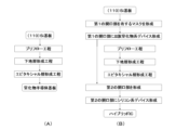
- FIG. 1 shows the flow of a method for manufacturing a nitride semiconductor substrate and a method for manufacturing a hybrid IC according to the present invention.
- 1 shows a comparison of the surface morphology of a gallium nitride epitaxial layer on a nitride semiconductor substrate in an example and a comparative example.
- a nitride semiconductor substrate using a silicon substrate whose principal surface has a ⁇ 110 ⁇ orientation and having a gallium nitride epitaxial layer with excellent surface morphology there has been a demand for a nitride semiconductor substrate using a silicon substrate whose principal surface has a ⁇ 110 ⁇ orientation and having a gallium nitride epitaxial layer with excellent surface morphology, a method for manufacturing the same, and a method for manufacturing a hybrid IC using a silicon substrate whose principal surface has a ⁇ 110 ⁇ orientation and having a group III nitride-based device and a silicon-based device that includes a gallium nitride epitaxial layer with excellent surface morphology.
- a method for manufacturing a nitride semiconductor substrate having a group III nitride layer including a group III nitride underlayer and a gallium nitride epitaxial layer on a silicon substrate, using a silicon substrate whose main surface has a surface orientation of ⁇ 110 ⁇ includes a preflow process for supplying a gas containing an aluminum raw material but not a nitrogen raw material onto the silicon substrate heated to 1000°C or higher, a base layer formation process for supplying a gas containing a group III raw material and a nitrogen raw material to form a group III nitride underlayer on the silicon substrate, and an epitaxial layer formation process for supplying a gas containing a gallium raw material and a nitrogen raw material to form a gallium nitride epitaxial layer, making it possible to manufacture a nitride semiconductor substrate having a gallium nitride epitaxial layer with
- the present inventors have discovered a method for manufacturing a hybrid IC in which silicon-based devices and Group III nitride-based devices coexist on the same silicon substrate, comprising the steps of: using a silicon substrate having a principal surface with a ⁇ 110 ⁇ orientation; forming a mask having a first opening in an area on the silicon substrate in which the Group III nitride-based devices are to be provided; and supplying a gas containing an aluminum raw material and not containing a nitrogen raw material onto the silicon substrate heated to 1000°C or higher in a preflow process; supplying a gas containing a Group III raw material and a nitrogen raw material to form a Group III nitride underlayer on the silicon substrate;
- the present invention was completed by discovering that a hybrid IC manufacturing method that performs an epitaxial layer formation process in which a gallium nitride epitaxial layer is formed by supplying a gas containing a nitrogen source, provides the III-nit
- a nitride semiconductor substrate according to the present invention will be described with reference to Fig. 1.
- a nitride semiconductor substrate 100 according to the present invention comprises a silicon substrate 1 and a Group III nitride layer 2 on the silicon substrate 1.
- the plane orientation of the principal surface of the silicon substrate 1 is ⁇ 110 ⁇ .
- the silicon substrate 1 is not particularly limited as long as the plane orientation of the principal surface is ⁇ 110 ⁇ .
- the plane orientation ⁇ 110 ⁇ includes a plane equivalent to (110).
- the plane orientation of the principal surface is ⁇ 110 ⁇
- the group III nitride layer 2 on the silicon substrate 1 includes a group III nitride underlayer 3 and a gallium nitride epitaxial layer 4 on the group III nitride underlayer 3.
- the roughness Ra of the surface 4a of the gallium nitride epitaxial layer 4 is 2.00 nm or less.
- the gallium nitride epitaxial layer 4 may be a multi-layer gallium nitride epitaxial layer having different dopant types and concentrations.
- the thickness of the gallium nitride epitaxial layer 4 is not particularly limited, but may be, for example, 0.8 ⁇ m or more and 10 ⁇ m or less.
- a gallium nitride epitaxial layer with a surface roughness Ra of 2.00 nm or less can be obtained reliably.
- the lower limit of the roughness Ra of the surface 4a of the gallium nitride epitaxial layer 4 is 0.00 nm or more.
- the III-nitride underlayer 3 may further include an initial layer 5 such as AlN on the surface of the silicon substrate 1, and a buffer layer 6 such as a graded composition layer or a superlattice layer.
- the nitride semiconductor substrate according to the present invention uses a silicon substrate 1 whose main surface has a ⁇ 110 ⁇ orientation, but has a surface morphology that is excellent and flat, with a roughness Ra of the surface 4a of the gallium nitride epitaxial layer 4 of 2.00 nm or less, making it a nitride semiconductor substrate suitable for Group III nitride devices.
- the method for manufacturing a nitride semiconductor substrate according to the present invention is a method for manufacturing a nitride semiconductor substrate 100 including a group III nitride layer 2 including a group III nitride underlayer 3 and a gallium nitride epitaxial layer 4 on a silicon substrate 1.
- the method for manufacturing a nitride semiconductor substrate according to the present invention uses a silicon substrate 1 whose principal surface has a plane orientation of ⁇ 110 ⁇ , and includes a preflow process in which a gas containing an aluminum source but not a nitrogen source is supplied onto the silicon substrate 1 heated to 1000°C or higher, an underlayer formation process in which a gas containing a Group III source and a nitrogen source is supplied to form a Group III nitride underlayer 3 on the silicon substrate 1, and an epitaxial layer formation process in which a gas containing a gallium source and a nitrogen source is supplied to form a gallium nitride epitaxial layer 4.
- a preflow process in which a gas containing an aluminum source but not a nitrogen source is supplied onto the silicon substrate 1 heated to 1000°C or higher
- an underlayer formation process in which a gas containing a Group III source and a nitrogen source is supplied to form a Group III nitride underlayer 3 on the silicon substrate 1
- an epitaxial layer formation process
- This step can be performed in a film forming apparatus that performs the subsequent underlayer forming step and epitaxial layer forming step.
- a silicon substrate 1 having a ⁇ 110 ⁇ surface orientation is heated to 1000° C. or higher, and a gas containing an aluminum raw material but not a nitrogen raw material is supplied. If a nitrogen raw material is contained, there is a risk that an AlN film will be formed, and the surface treatment before the underlayer formation of the silicon substrate 1 using the aluminum raw material will not be performed, and there will be no flattening effect on the surface of the gallium nitride epitaxial layer 4.
- the temperature to which the silicon substrate 1 is heated may be 1000°C or higher, and the technical upper limit is below the melting point of the silicon substrate 1, but it is preferable to set it to 1200°C or lower. Even if the temperature is set too high, the effect of the preflow process does not change significantly, but damage to the Si substrate and components of the film formation device can be more stably suppressed, so a temperature of 1200°C or lower is sufficient when the stability and productivity of the preflow process are taken into consideration.
- the time for supplying the gas containing the aluminum raw material and not containing the nitrogen raw material is not particularly limited.
- the lower limit can be, for example, 1 second or more, preferably 3 seconds or more, and more preferably 5 seconds or more.
- the upper limit can be, for example, 60 seconds or less, preferably 30 seconds or less, and more preferably 15 seconds or less. Within such a range, the effect of planarizing the surface of the gallium nitride epitaxial layer 4 can be obtained more stably.
- the gas containing an aluminum source but not a nitrogen source used in the preflow process is not particularly limited.
- an organoaluminum compound is preferably used as the aluminum source.
- the organoaluminum compound include trimethylaluminum (TMA) and triethylaluminum (TEA). These are used as film-forming materials for III-nitrides, and the same gas can be used when using an organoaluminum compound in the subsequent underlayer formation process, etc., so that it is suitable in terms of cost and for preventing contamination of the substrate and growth device.
- hydrogen (H 2 ) gas can be used as a carrier gas.
- the inventors have investigated the reason why the surface roughness Ra of the surface of the gallium nitride epitaxial layer is 2.00 nm or less and the surface can be made mirror-like by performing such a preflow process.
- the Al layer which is thought to have been formed very thinly, will be altered before analysis, and it is also believed that the structure affected by the preflow process will change due to heat treatment and other processes after the preflow process after the nitride semiconductor substrate is manufactured, and it was not possible to clearly determine the difference in the structure of the silicon substrate surface depending on whether or not the preflow process is performed.
- the surface of the gallium nitride epitaxial layer can be made mirror-like with a roughness Ra of 2.00 nm or less by performing the preflow process is unclear, but it is possible that the preflow process forms an extremely thin Al layer of about several angstroms, and the eutectic reaction with Si forms fine irregularities on the surface, which causes the ⁇ 111 ⁇ plane to appear and promotes the lateral growth of the III-nitride layer such as GaN.
- the surface roughness Ra of the surface of the gallium nitride epitaxial layer can be reduced to 2.00 nm or less, resulting in a mirror surface.
- a gas containing a Group III source and a nitrogen source is supplied to form a Group III nitride underlayer 3, which is a part of the Group III nitride layer 2, on the silicon substrate 1.
- a gas containing a Group III source and a nitrogen source is supplied to form a Group III nitride underlayer 3, which is a part of the Group III nitride layer 2, on the silicon substrate 1.
- an initial layer 5 such as AlN, or a buffer layer 6 such as a graded composition layer or a superlattice layer can be formed.
- the conditions for forming the Group III nitride underlayer 3 are not particularly limited.
- a gas containing a gallium source and a nitrogen source is supplied to form a gallium nitride epitaxial layer 4, and an epitaxial layer formation process is performed.
- the conditions for forming the gallium nitride epitaxial layer 4 are not particularly limited.
- the gallium nitride epitaxial layer 4 may be formed by MOCVD or HVPE.
- the gallium source an organic gallium compound such as trimethylgallium (TMG) or triethylgallium (TEG) may be used.
- TMG trimethylgallium
- TMG triethylgallium
- a plurality of gallium nitride epitaxial layers may be formed by changing the type and concentration of the dopant.
- a method for manufacturing a hybrid IC according to the present invention will be described with reference to FIG. 2B.
- a silicon substrate with a surface orientation of ⁇ 110 ⁇ is used.
- a mask having a first opening is formed on the silicon substrate, and a group III nitride device such as an electronic device or a light emitting device is provided in the first opening.
- the mask in the region where the silicon device is to be provided is removed to form a second opening, and the silicon device is provided in the second opening.
- a Group III nitride device is formed in a first opening.
- the "preflow step,”"underlayer formation step,” and “epitaxial layer formation step” described in the nitride semiconductor substrate manufacturing method are performed. Detailed descriptions of these steps are omitted since they are the same as those in the nitride semiconductor substrate manufacturing method.
- a silicon-based device is formed in the second opening.
- the silicon-based device it is preferable to fabricate a FinFET or GAA in order to take advantage of the advantages of using a Si ⁇ 110 ⁇ substrate.
- a Si (110) substrate is prepared.
- the substrate surface is cleaned by hydrogen (H 2 ) baking halfway through raising the temperature of the Si substrate to the growth temperature.
- H 2 hydrogen
- TMA preflow is performed, for example, within 60 seconds.
- the initial layer AlN and a buffer layer that is an Al x Ga 1-x N (x ⁇ 0) layer are formed, and an island-shaped SiN layer is formed, and then a GaN layer is laminated.
- an AlGaN layer can be formed on a GaN layer to form a HEMT structure.
- a GaN/InGaN MQW structure can be fabricated on a buffer layer that is an Al x Ga 1-x N (x ⁇ 0) layer, and p-GaN can be formed to form a light-emitting device.
- the buffer layer may have a graded composition or may be made of a plurality of layers of different compositions, for example, a stepwise composition AlGaN layer, a superlattice AlGaN/GaN, a superlattice AlGaN/GaN, or an intermittent superlattice structure.
- Nitrogen (N 2 ) gas is switched to hydrogen (H 2 ) gas while the temperature of the Si substrate is raised to the growth temperature (1000-1200° C.), and the substrate surface is cleaned by hydrogen (H 2 ) baking while the temperature is raised.
- TMA is supplied at 1000-1200° C. to perform a preflow process.
- TMA+NH 3 gas is supplied to form an initial layer AlN with a thickness of 100-200 nm
- TMA+TMG (trimethylgallium)+NH 3 gas is supplied to form a buffer layer of an AlGaN layer with a thickness of 100-200 nm.
- TMA and TMG are interrupted, and SiH 4 +NH 3 is supplied to form an island-shaped SiN layer.
- the supply of monosilane gas is stopped, and TMG is flowed to grow a GaN layer to a thickness of 15-50 nm.
- a superlattice (SLs) buffer layer of 15 to 25 pairs of AlN/GaN is formed, followed by forming a GaN layer with a thickness of about 800 to 900 nm to obtain a nitride semiconductor substrate.
- Second Embodiment A specific example of a method for manufacturing a hybrid IC according to the present invention will be given below as the second embodiment.
- a Si (110) substrate is prepared.
- a thermal oxide film is formed to a thickness of about 100 nm on the surface of the Si substrate, a mask is formed using photolithography on the portion where the Si device is to be manufactured, and the oxide film is removed by dry etching from the portion where the gallium nitride epitaxial layer is to be grown, exposing the Si substrate only in the portion where the III-nitride device is to be manufactured (first opening).
- the subsequent manufacturing process for the III-nitride device is the same as in the first embodiment.
- the GaN film that has been poly-grown on the oxide film in the area where the silicon devices will be fabricated is removed by dry etching to protect the III-nitride (GaN) device area.
- the oxide layer is removed by immersion in HF liquid to expose the Si substrate (second opening). Silicon devices are fabricated on the exposed Si substrate.
- a Si (110) substrate with a diameter of 150 mm, p-type (boron concentration 6 ⁇ 10 14 atoms/cm 3 or less), and oxygen concentration 7 ⁇ 10 17 atoms/cm 3 was prepared.
- the Si (110) substrate was carried into an MOCVD apparatus, and hydrogen was used as the carrier gas.
- TMA trimethylaluminum preflow was performed for 6 seconds.
- ammonia gas which is a nitrogen source
- TMG trimethylgallium
- the supply of TMA and TMG was interrupted, monosilane gas was flowed, and an SiN layer was grown in an island shape to a thickness of 1 nm, after which the supply of monosilane gas was stopped, and TMG was flowed to grow a GaN layer to a thickness of 25 nm.
- a 4.2 nm AlN/25 nm GaN layer was grown on top of the buffer layer with a thickness of 400 nm and a 23-pair SLs structure, on which a 820 nm GaN layer was grown to form a gallium nitride epitaxial layer.
- Comparative Example A gallium nitride epitaxial layer was formed using the same steps and conditions as in the example, except that preflow using TMA was not performed.
- the surface morphology of the gallium nitride epitaxial layer was evaluated. Specifically, the presence or absence of cloudiness was evaluated by visual observation with a condenser lamp, and observation was performed with a differential interference microscope. As a result of observation with a condenser lamp, cloudiness was observed on the surface of the gallium nitride epitaxial layer of the comparative example, whereas no cloudiness was observed on the surface of the gallium nitride epitaxial layer of the example, and it was found to be a mirror surface. Furthermore, as a result of observation with a differential interference microscope, as shown in FIG.
- a nitride semiconductor substrate having a gallium nitride epitaxial layer with a flat surface and good surface morphology, with the surface roughness Ra of the gallium nitride epitaxial layer being 2.00 nm or less.
- the present invention is not limited to the above-described embodiments.
- the above-described embodiments are merely examples, and anything that has substantially the same configuration as the technical idea described in the claims of the present invention and exhibits similar effects is included within the technical scope of the present invention.
Landscapes
- Chemical & Material Sciences (AREA)
- Engineering & Computer Science (AREA)
- Crystallography & Structural Chemistry (AREA)
- Materials Engineering (AREA)
- Metallurgy (AREA)
- Organic Chemistry (AREA)
- Inorganic Chemistry (AREA)
- Chemical Kinetics & Catalysis (AREA)
- General Chemical & Material Sciences (AREA)
- Chemical Vapour Deposition (AREA)
- Crystals, And After-Treatments Of Crystals (AREA)
- Recrystallisation Techniques (AREA)
Abstract
Description
本発明に係る窒化物半導体基板について図1を参照しながら説明する。本発明に係る窒化物半導体基板100は、シリコン基板1と、シリコン基板1上にIII族窒化物層2を備えるものである。
次に、本発明に係る窒化物半導体基板の製造方法について図2(A)を参照しながら説明する。本発明に係る窒化物半導体基板の製造方法は、シリコン基板1上にIII族窒化物下地層3と窒化ガリウムエピタキシャル層4とを含むIII族窒化物層2を備えた窒化物半導体基板100の製造方法である。
この工程は、後続の下地層形成工程やエピタキシャル層形成工程を行う成膜装置内で行うことができる。主面の面方位が{110}のシリコン基板1を1000℃以上に加熱し、アルミニウム原料を含み窒素原料を含まないガスを供給する。窒素原料を含んでいると、AlNが成膜してしまう恐れがあり、アルミニウム原料によるシリコン基板1の下地層形成前の表面処理とはならず、窒化ガリウムエピタキシャル層4の表面の平坦化効果がない。
次に、下地層形成工程について説明する。上述のプリフロー工程の後、III族原料及び窒素原料を含むガスを供給して、シリコン基板1上にIII族窒化物層2の一部であるIII族窒化物下地層3を形成する。III族窒化物下地層3としては、AlNなどの初期層5や、傾斜組成層、超格子層などのバッファ層6を形成することができる。III族窒化物下地層3の形成条件は特に限定されない。
下地層形成工程の後、ガリウム原料及び窒素原料を含むガスを供給して窒化ガリウムエピタキシャル層4を形成するエピタキシャル層形成工程を行う。窒化ガリウムエピタキシャル層4の形成条件は特に限定されない。例えばMOCVD法やHVPE法などにより、窒化ガリウムエピタキシャル層4を形成すればよい。ガリウム原料としては、トリメチルガリウム(TMG)やトリエチルガリウム(TEG)などの有機ガリウム化合物を使用することができる。なお、窒化ガリウムエピタキシャル層4として、ドーパントの種類や濃度を変えて複数層の窒化ガリウムエピタキシャル層を形成してもよい。
次に、本発明に係るハイブリッドICの製造方法について図2(B)を参照しながら説明する。本発明に係るハイブリッドICの製造方法では、主面の面方位が{110}であるシリコン基板を用いる。そして、このシリコン基板上に第1の開口部を有するマスクを形成し、第1の開口部に電子デバイスや発光デバイスなどのIII族窒化物系デバイスを設ける。その後、シリコン系デバイスを設ける領域のマスクを除去して第2の開口部を形成し、この第2の開口部にシリコン系デバイスを設ける。これにより、正孔の移動度の上がる<110>シリコン基板上に、表面モフォロジーが良好な鏡面を有する窒化ガリウムエピタキシャル層を備えたIII族窒化物系デバイスと、FinFET(Fin Field-Effect Transistor)やGAA(Gate-All-Around)などのシリコン系デバイスとが共存したハイブリッドICを製造することができる。
本発明に係るハイブリッドICの製造方法におけるIII族窒化物系デバイスの形成では、第1の開口部にIII族窒化物系デバイスを形成する。そして、このIII族窒化物系デバイスの形成では、窒化物半導体基板の製造方法で説明した「プリフロー工程」、「下地層形成工程」、「エピタキシャル層形成工程」を行う。これらの工程の詳細についての説明は、窒化物半導体基板の製造方法と同様であるので割愛する。
本発明に係るハイブリッドICの製造方法におけるシリコン系デバイスの形成では、第2の開口部にシリコン系デバイスを形成する。シリコン系デバイスとしては特に限定されないが、Si{110}基板を用いる利点を活かすため、FinFETやGAAを作製することが好ましい。
以下に、第1の実施形態として、本発明に係る窒化物半導体基板の製造方法の具体例を挙げる。まず、Si(110)基板を準備する。成長温度までSi基板を昇温する途中から水素(H2)ベイクによる基板表面のクリーニングを行う。そして、初期層AlNの成長を開始する前にTMAのプリフローを例えば60秒以内で行う。その後、初期層AlN、AlxGa1-xN(x≧0)層であるバッファ層を形成し、アイランド状のSiN層を形成してからGaN層を積層する。電子デバイス用にはGaN層の上にAlGaN層を形成しHEMT構造とできる。発光デバイスでは、AlxGa1-xN(x≧0)層であるバッファ層の上にGaN/InGaNのMQW構造を作製し、p-GaNを形成して発光デバイスとすることができる。なお上記バッファ層は、傾斜的に組成変化したり、異なる組成の複数層からなってもよく、例えば、階段組成AlGaN層、超格子AlGaN/GaN、超格子AlN/GaN、間欠超格子構造としても良い。
以下に、第2の実施形態として、本発明に係るハイブリッドICの製造方法の具体例を挙げる。まず、Si(110)基板を準備する。Si基板表面に熱酸化膜を100nm程度形成しSiデバイスを作製する部分にフォトリソを使用してマスクを形成し、ドライエッチングにて窒化ガリウムエピタキシャル層を成長させる部分の酸化膜を削除して、III族窒化物系デバイスを作製する部分のみSi基板を露出させておく(第1の開口部)。この後のIII族窒化物系デバイスの製造は、第1の実施形態と同様である。
GaN on Siのエピタキシャル成長用基板として、直径150mmのp型(ボロン濃度6×10¹⁴atoms/cm3以下)、酸素濃度7×1017atoms/cm3のSi(110)基板を準備した。Si(110)基板をMOCVD装置に搬入して、キャリアガスを水素とし、エピタキシャル成長温度の1150℃に達したらTMA(トリメチルアルミニウム)のプリフローを6秒間行った。その後、窒素源であるアンモニアガスを流し、初期層AlNを150nm、その後TMG(トリメチルガリウム)も流してAlGaN層を160nm形成した。TMA、TMG供給を中断し、モノシランガスを流して、アイランド状にSiN層を1nm成長させてから、モノシランガスの供給を停止し、TMGを流してGaN層を25nm成長させた。その上に4.2nmのAlN/25nmのGaN層が23ペアのSLs構造の厚さ400nmのバッファ層を形成した。その上に820nmのGaN層を成長し、窒化ガリウムエピタキシャル層を形成した。
TMAを用いたプリフローを行わなかったこと以外は実施例と同じ工程、条件で窒化ガリウムエピタキシャル層を形成した。
まず、窒化ガリウムエピタキシャル層の表面モフォロジーの評価を行った。具体的には、目視による集光灯観察での曇りの有無の評価及び微分干渉顕微鏡による観察を行った。集光灯観察の結果、比較例の窒化ガリウムエピタキシャル層表面には曇りが観察されたのに対し、実施例の窒化ガリウムエピタキシャル層表面には曇りは観察されず、鏡面であることがわかった。また、微分干渉顕微鏡による観察の結果、図3に示すように、比較例の窒化ガリウムエピタキシャル層表面には凹凸が観察されたのに対し、実施例の窒化ガリウムエピタキシャル層表面は平滑であることがわかった。さらに、窒化ガリウムエピタキシャル層表面の表面粗さを、触針式プロファイラー(KLA-Tencor社製、P-15)を用いて測定したところ、実施例ではRa1.86nm、比較例ではRa12.5nmとなった。本願の実施例によれば、Ra2.00nm以下の表面粗さで、鏡面の窒化ガリウムエピタキシャル層を得ることができた。
Claims (7)
- シリコン基板上にIII族窒化物下地層と窒化ガリウムエピタキシャル層とを含むIII族窒化物層を備えた窒化物半導体基板の製造方法であって、
主面の面方位が{110}であるシリコン基板を用い、
1000℃以上に加熱した前記シリコン基板上に、アルミニウム原料を含み窒素原料を含まないガスを供給するプリフロー工程と、
III族原料及び窒素原料を含むガスを供給して前記シリコン基板上にIII族窒化物下地層を形成する下地層形成工程と、
ガリウム原料及び窒素原料を含むガスを供給して窒化ガリウムエピタキシャル層を形成するエピタキシャル層形成工程とを含むことを特徴とする窒化物半導体基板の製造方法。 - 前記アルミニウム原料として有機アルミニウム化合物を用いることを特徴とする請求項1に記載の窒化物半導体基板の製造方法。
- 前記プリフロー工程における前記シリコン基板の加熱温度を1200℃以下とすることを特徴とする請求項1又は2に記載の窒化物半導体基板の製造方法。
- 同一のシリコン基板上にシリコン系デバイスとIII族窒化物系デバイスが共存するハイブリッドICの製造方法であって、
主面の面方位が{110}であるシリコン基板を用い、該シリコン基板上の前記III族窒化物系デバイスを設ける領域に第1の開口部を有するマスクを形成し、
1000℃以上に加熱した前記シリコン基板上に、アルミニウム原料を含み窒素原料を含まないガスを供給するプリフロー工程と、
III族原料及び窒素原料を含むガスを供給して前記シリコン基板上にIII族窒化物下地層を形成する下地層形成工程と、
ガリウム原料及び窒素原料を含むガスを供給して窒化ガリウムエピタキシャル層を形成するエピタキシャル層形成工程を行い、前記第1の開口部に前記III族窒化物系デバイスを設け、
その後、前記シリコン系デバイスを設ける領域の前記マスクを除去して第2の開口部を形成し、該第2の開口部に前記シリコン系デバイスを設けることを特徴とするハイブリッドICの製造方法。 - 前記アルミニウム原料として有機アルミニウム化合物を用いることを特徴とする請求項4に記載のハイブリッドICの製造方法。
- 前記プリフロー工程における前記シリコン基板の加熱温度を1200℃以下とすることを特徴とする請求項4又は5に記載のハイブリッドICの製造方法。
- シリコン基板上にIII族窒化物層を備えた窒化物半導体基板であって、
前記シリコン基板の主面の面方位は{110}であり、
前記シリコン基板上の前記III族窒化物層は、III族窒化物下地層と、該III族窒化物下地層上の窒化ガリウムエピタキシャル層とを備えるものであり、
前記窒化ガリウムエピタキシャル層の表面の粗さRaは2.00nm以下であることを特徴とする窒化物半導体基板。
Priority Applications (3)
| Application Number | Priority Date | Filing Date | Title |
|---|---|---|---|
| KR1020257040184A KR20260019483A (ko) | 2023-06-01 | 2024-05-21 | 질화물 반도체 기판의 제조방법, 하이브리드 ic의 제조방법 및 질화물 반도체 기판 |
| CN202480035387.6A CN121195330A (zh) | 2023-06-01 | 2024-05-21 | 氮化物半导体基板的制造方法、混合集成电路的制造方法及氮化物半导体基板 |
| EP24815312.4A EP4723162A1 (en) | 2023-06-01 | 2024-05-21 | Method for manufacturing nitride semiconductor substrate, method for manufacturing hybrid ic, and nitride semiconductor substrate |
Applications Claiming Priority (2)
| Application Number | Priority Date | Filing Date | Title |
|---|---|---|---|
| JP2023090721A JP2024172767A (ja) | 2023-06-01 | 2023-06-01 | 窒化物半導体基板の製造方法、ハイブリッドicの製造方法及び窒化物半導体基板 |
| JP2023-090721 | 2023-06-01 |
Publications (1)
| Publication Number | Publication Date |
|---|---|
| WO2024247828A1 true WO2024247828A1 (ja) | 2024-12-05 |
Family
ID=93657302
Family Applications (1)
| Application Number | Title | Priority Date | Filing Date |
|---|---|---|---|
| PCT/JP2024/018747 Ceased WO2024247828A1 (ja) | 2023-06-01 | 2024-05-21 | 窒化物半導体基板の製造方法、ハイブリッドicの製造方法及び窒化物半導体基板 |
Country Status (6)
| Country | Link |
|---|---|
| EP (1) | EP4723162A1 (ja) |
| JP (1) | JP2024172767A (ja) |
| KR (1) | KR20260019483A (ja) |
| CN (1) | CN121195330A (ja) |
| TW (1) | TW202514756A (ja) |
| WO (1) | WO2024247828A1 (ja) |
Citations (2)
| Publication number | Priority date | Publication date | Assignee | Title |
|---|---|---|---|---|
| JP2009503871A (ja) * | 2005-07-26 | 2009-01-29 | アンバーウェーブ システムズ コーポレイション | 代替活性エリア材料の集積回路への組み込みのための解決策 |
| JP2022025512A (ja) | 2020-07-29 | 2022-02-10 | 信越半導体株式会社 | 窒化物半導体ウェーハおよび窒化物半導体ウェーハの製造方法 |
-
2023
- 2023-06-01 JP JP2023090721A patent/JP2024172767A/ja active Pending
-
2024
- 2024-05-21 KR KR1020257040184A patent/KR20260019483A/ko active Pending
- 2024-05-21 CN CN202480035387.6A patent/CN121195330A/zh active Pending
- 2024-05-21 WO PCT/JP2024/018747 patent/WO2024247828A1/ja not_active Ceased
- 2024-05-21 EP EP24815312.4A patent/EP4723162A1/en active Pending
- 2024-05-24 TW TW113119299A patent/TW202514756A/zh unknown
Patent Citations (2)
| Publication number | Priority date | Publication date | Assignee | Title |
|---|---|---|---|---|
| JP2009503871A (ja) * | 2005-07-26 | 2009-01-29 | アンバーウェーブ システムズ コーポレイション | 代替活性エリア材料の集積回路への組み込みのための解決策 |
| JP2022025512A (ja) | 2020-07-29 | 2022-02-10 | 信越半導体株式会社 | 窒化物半導体ウェーハおよび窒化物半導体ウェーハの製造方法 |
Non-Patent Citations (2)
| Title |
|---|
| MATSUMOTO, KOH; YAMAOKA, YUYA: "Impact of the AlN Nucleation Layer on GaN grown on Silicon Substrate by MOCVD for Power-devices", THE JOURNAL OF THE INSTITUTE OF ELECTRICAL ENGINEERS OF JAPAN, vol. 137, no. 10, 1 October 2017 (2017-10-01), Japan , pages 681 - 684, XP009560075, ISSN: 1340-5551, DOI: 10.1541/ieejjournal.137.681 * |
| SHIMANAKA, K. : "MOCVD growth of GaN thin films on Si(110)substrates", LECTURE PREPRINTS OF 55TH MEETING OF THE JAPAN SOCIETY OF APPLIED PHYSICS AND RELATED SOCIETIES, THE JAPAN SOCIETY OF APPLIED PHYSICS (JSAP), vol. 55, no. 1, 1 January 2008 (2008-01-01), pages 409, XP009560074 * |
Also Published As
| Publication number | Publication date |
|---|---|
| JP2024172767A (ja) | 2024-12-12 |
| TW202514756A (zh) | 2025-04-01 |
| EP4723162A1 (en) | 2026-04-08 |
| CN121195330A (zh) | 2025-12-23 |
| KR20260019483A (ko) | 2026-02-10 |
Similar Documents
| Publication | Publication Date | Title |
|---|---|---|
| CN101896997B (zh) | 半导体基板、半导体基板的制造方法及电子器件 | |
| CN104205298B (zh) | 在硅基板上形成iii/v族共形层的方法 | |
| TWI506675B (zh) | 半導體基板、半導體基板之製造方法及電子裝置 | |
| JP3550070B2 (ja) | GaN系化合物半導体結晶、その成長方法及び半導体基材 | |
| TWI442454B (zh) | 用於製備化合物半導體基底的方法 | |
| KR101878754B1 (ko) | 대면적 갈륨 나이트라이드 기판 제조방법 | |
| JP2006128626A (ja) | 窒化物系半導体装置及びその製造方法 | |
| WO2009084240A1 (ja) | 半導体基板、半導体基板の製造方法および電子デバイス | |
| JP4860736B2 (ja) | 半導体構造物及びそれを製造する方法 | |
| JP4449357B2 (ja) | 電界効果トランジスタ用エピタキシャルウェハの製造方法 | |
| KR20140106590A (ko) | 반도체 기판 및 형성 방법 | |
| JP6090899B2 (ja) | エピタキシャルウェハの製造方法 | |
| CN1697134A (zh) | 一种利用SiN膜原位制备图形衬底的方法 | |
| CN101728248A (zh) | 氮化镓生长方法 | |
| JP2024172767A (ja) | 窒化物半導体基板の製造方法、ハイブリッドicの製造方法及び窒化物半導体基板 | |
| CN106229388A (zh) | 一种氮化镓基发光二极管的外延片的制备方法 | |
| CN103872200A (zh) | 形成半导体层的方法、半导体发光器件及其制造方法 | |
| CN106887495A (zh) | 发光二极管的外延片及其制作方法 | |
| KR100834698B1 (ko) | 질화 갈륨 박막 형성 방법 및 이 방법에 의해 제조된 질화갈륨 박막 기판 | |
| JP2017130539A (ja) | 窒化物半導体装置、窒化物半導体装置の作製方法、及び製造装置 | |
| US20130020549A1 (en) | Systems and methods for fabricating longitudinally-shaped structures | |
| TW201513176A (zh) | 半導體晶圓以及生產半導體晶圓的方法 | |
| JPH09293678A (ja) | InGaN層を有する半導体ウエハ及びその製造方法並びにそれを具備する発光素子 | |
| CN109378368B (zh) | 在PSS衬底上沿半极性面外延生长GaN基片的方法 | |
| JP2022131981A (ja) | 半導体成長用基板の製造方法、半導体成長用基板、半導体素子および半導体発光素子 |
Legal Events
| Date | Code | Title | Description |
|---|---|---|---|
| 121 | Ep: the epo has been informed by wipo that ep was designated in this application |
Ref document number: 24815312 Country of ref document: EP Kind code of ref document: A1 |
|
| WWE | Wipo information: entry into national phase |
Ref document number: 2024815312 Country of ref document: EP |
|
| NENP | Non-entry into the national phase |
Ref country code: DE |
|
| ENP | Entry into the national phase |
Ref document number: 2024815312 Country of ref document: EP Effective date: 20260102 |
|
| ENP | Entry into the national phase |
Ref document number: 2024815312 Country of ref document: EP Effective date: 20260102 |
|
| ENP | Entry into the national phase |
Ref document number: 2024815312 Country of ref document: EP Effective date: 20260102 |
|
| ENP | Entry into the national phase |
Ref document number: 2024815312 Country of ref document: EP Effective date: 20260102 |
|
| ENP | Entry into the national phase |
Ref document number: 2024815312 Country of ref document: EP Effective date: 20260102 |
|
| ENP | Entry into the national phase |
Ref document number: 2024815312 Country of ref document: EP Effective date: 20260102 |
|
| WWP | Wipo information: published in national office |
Ref document number: 2024815312 Country of ref document: EP |