WO2024247739A1 - 半導体装置 - Google Patents
半導体装置 Download PDFInfo
- Publication number
- WO2024247739A1 WO2024247739A1 PCT/JP2024/018095 JP2024018095W WO2024247739A1 WO 2024247739 A1 WO2024247739 A1 WO 2024247739A1 JP 2024018095 W JP2024018095 W JP 2024018095W WO 2024247739 A1 WO2024247739 A1 WO 2024247739A1
- Authority
- WO
- WIPO (PCT)
- Prior art keywords
- metal plate
- resin member
- terminal
- semiconductor chip
- control circuit
- Prior art date
- Legal status (The legal status is an assumption and is not a legal conclusion. Google has not performed a legal analysis and makes no representation as to the accuracy of the status listed.)
- Ceased
Links
Images


Classifications
-
- H—ELECTRICITY
- H10—SEMICONDUCTOR DEVICES; ELECTRIC SOLID-STATE DEVICES NOT OTHERWISE PROVIDED FOR
- H10W—GENERIC PACKAGES, INTERCONNECTIONS, CONNECTORS OR OTHER CONSTRUCTIONAL DETAILS OF DEVICES COVERED BY CLASS H10
- H10W70/00—Package substrates; Interposers; Redistribution layers [RDL]
- H10W70/60—Insulating or insulated package substrates; Interposers; Redistribution layers
- H10W70/67—Insulating or insulated package substrates; Interposers; Redistribution layers characterised by their insulating layers or insulating parts
- H10W70/68—Shapes or dispositions thereof
-
- H—ELECTRICITY
- H10—SEMICONDUCTOR DEVICES; ELECTRIC SOLID-STATE DEVICES NOT OTHERWISE PROVIDED FOR
- H10W—GENERIC PACKAGES, INTERCONNECTIONS, CONNECTORS OR OTHER CONSTRUCTIONAL DETAILS OF DEVICES COVERED BY CLASS H10
- H10W72/00—Interconnections or connectors in packages
-
- H—ELECTRICITY
- H10—SEMICONDUCTOR DEVICES; ELECTRIC SOLID-STATE DEVICES NOT OTHERWISE PROVIDED FOR
- H10W—GENERIC PACKAGES, INTERCONNECTIONS, CONNECTORS OR OTHER CONSTRUCTIONAL DETAILS OF DEVICES COVERED BY CLASS H10
- H10W90/00—Package configurations
Definitions
- Patent Document 1 Patent Document 2, Patent Document 3
- the semiconductor device includes a first metal plate having electrical conductivity, a semiconductor chip disposed on the first metal plate and electrically connected to the first metal plate, and a control circuit metal plate that is disposed at a position different from the first metal plate in the thickness direction of the semiconductor chip, has electrical conductivity, and constitutes a control circuit for controlling the semiconductor device.
- the control circuit includes at least one of a gate circuit, an auxiliary source circuit, a temperature characteristic detection circuit, and an electrical characteristic detection circuit.
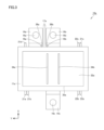
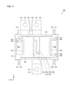
- FIG. 1 is a schematic perspective view of a semiconductor device according to a first embodiment.
- FIG. 2 is a schematic plan view of the semiconductor device shown in FIG.
- FIG. 3 is a schematic bottom view of the semiconductor device shown in FIG.
- FIG. 4 is a schematic front view of the semiconductor device shown in FIG.
- FIG. 5 is a schematic rear view of the semiconductor device shown in FIG.
- FIG. 6 is a schematic left side view of the semiconductor device shown in FIG.
- FIG. 7 is a schematic right side view of the semiconductor device shown in FIG.
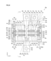
- FIG. 8 is a schematic perspective view showing a state in which a first resin member, which will be described later, has been removed from the semiconductor device shown in FIG.
- FIG. 9 is a schematic plan view of the semiconductor device shown in FIG. FIG.
- FIG. 10 is a schematic cross-sectional view taken along the line XX in FIG.
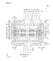
- FIG. 11 is a schematic plan view showing a DBC substrate on which eight semiconductor chips, which will be described later, are mounted.
- FIG. 12 is a schematic cross-sectional view of the DBC substrate shown in FIG. 11 taken along the line indicated by XII-XII in FIG.
- FIG. 13 is a schematic perspective view showing an enlarged area where the insert metal is placed.
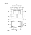
- FIG. 14 is a schematic plan view showing an enlarged view of a part of a semiconductor device in which a solder resist is provided on a control circuit metal plate.
- FIG. 15 is a schematic perspective view showing a state in which the first resin member has been removed in the semiconductor device according to the second embodiment of the present disclosure.
- FIG. 16 is a schematic plan view of the semiconductor device shown in FIG.
- FIG. 17 is a schematic bottom view of the semiconductor device shown in FIG. 18 is a schematic bottom view showing an enlarged portion of the inside of the semiconductor device shown in FIG.
- FIG. 19 is a schematic perspective view showing a semiconductor device according to the third embodiment of the present disclosure.
- one of the objectives is to provide a semiconductor device that can ensure stable operation while being compact.
- a semiconductor device includes a first metal plate having electrical conductivity, a semiconductor chip disposed on the first metal plate and electrically connected to the first metal plate, and a control circuit metal plate disposed at a position different from the first metal plate in a thickness direction of the semiconductor chip, having electrical conductivity, and constituting a control circuit for controlling the semiconductor device.
- the control circuit includes at least one of a gate circuit, an auxiliary source circuit, a temperature characteristic detection circuit, and an electrical characteristic detection circuit.
- the control circuit formed by the control circuit metal plate includes at least one of the gate circuit, the auxiliary source circuit, the temperature characteristic detection circuit, and the electrical characteristic detection circuit, so that the semiconductor device can be controlled more precisely.
- the control circuit metal plate constituting the control circuit including at least one of the gate circuit, the auxiliary source circuit, the temperature characteristic detection circuit, and the electrical characteristic detection circuit is disposed at a position different from the first metal plate on which the semiconductor chip is mounted in the thickness direction of the semiconductor chip. In this way, the first metal plate can be greatly expanded while suppressing the increase in the overall size of the semiconductor device in the direction perpendicular to the thickness direction of the first metal plate.
- the control circuit metal plate regardless of the size of the control circuit metal plate, the area of the first metal plate that contributes to improving the heat dissipation of the semiconductor chip can be increased. Furthermore, since the control circuit metal plate is disposed at a position different from the semiconductor chip that becomes hot, thermal interference from the semiconductor chip can also be prevented. Therefore, stable operation can be ensured while achieving compactness of the semiconductor device.
- the control circuit metal plate does not necessarily have to adopt the configuration of a substrate including an insulating layer, so there is no restriction on the heat resistance of the insulating layer when an insulating layer is included during the manufacture of the semiconductor device, etc. Furthermore, if the insulating layer can be omitted, costs can be reduced. Furthermore, omitting the insulating layer relaxes the dimensional restrictions in the thickness direction of the control circuit metal plate, and the thickness of the control circuit metal plate can be increased to reduce parasitic resistance and parasitic inductance, ensuring more stable operation. Furthermore, if the insulating layer can be omitted, the control circuit metal plate can be metallically bonded to other metal components, improving productivity.
- control circuit metal plate may include an area that overlaps with the first metal plate when viewed in the thickness direction of the semiconductor chip. This allows the first metal plate to be made larger while effectively utilizing the area in the thickness direction of the semiconductor chip where the control circuit metal plate is located. This allows for more reliable compactness while improving heat dissipation.
- a first resin member that seals the semiconductor chip may be further provided.
- the control circuit metal plate may include a first terminal having a portion exposed from the first resin member, and a first frame having a portion covered by the first resin member.
- the first terminal and the first frame may be integrally configured. In this manner, the first terminal can be arranged at the same time by holding the first frame, which is included in the control circuit metal plate and integrally configured with the first terminal, with the second resin member described below, improving assembly during manufacturing.
- integral means that the first terminal and the first frame are manufactured from a single member, rather than being manufactured by combining multiple members by bonding, connecting with screws, or the like.
- a first resin member that seals the semiconductor chip may be further provided.
- the control circuit metal plate may include a first terminal having a portion exposed from the first resin member, and a first frame having a portion covered by the first resin member.
- the first terminal and the first frame may be configured as separate bodies.
- the first terminal may be held by the second resin member. In this way, by metal-joining the first frame, it is possible to fix the first frame and simultaneously establish an electrical connection.
- “separate bodies” is a concept that is opposed to the above-mentioned "integral body," and the first terminal and the first frame are not manufactured from a single member, but are manufactured by combining multiple members by bonding, connecting with screws, etc.
- a first resin member that seals the semiconductor chip and a second resin member that is provided separately from the first resin member may be further provided.
- the control circuit metal plate may be disposed on the second resin member. In this way, the control circuit metal plate can be positioned by the second resin member and fixed. Therefore, a manufacturing jig is not required, and productivity can be improved.
- the second resin member functions as a base. Therefore, ultrasonic vibrations are applied efficiently, and stable bonding can be ensured.
- the second resin member is an insulator, it can be disposed in a state where insulation from the first metal plate is ensured, and stable operation can be ensured.
- the semiconductor device may further include a first resin member that seals the semiconductor chip, and a second resin member that is provided separately from the first resin member.
- the control circuit metal plate may include a first terminal having a protruding portion protruding from the second resin member and a holding portion held by the second resin member, and a first frame having a portion covered by the first resin member.
- the holding portion may include a terminal exposed portion exposed from the second resin member.
- the first frame may be joined to the first terminal in a region where the terminal exposed portion is located when viewed in the thickness direction of the semiconductor chip.
- the metals of the first terminal and the first frame overlap each other in the terminal exposed portion, making it possible to perform metal joining such as fusion joining by laser welding or liquid phase joining by solder or brazing material, and to achieve electrical connection at the same time as fixing. This allows the joining time to be shortened, thereby improving productivity.
- the semiconductor device may further include a first resin member that seals the semiconductor chip, a second resin member that is provided separately from the first resin member, and an insert metal that is held by the second resin member and joined to the control circuit metal plate.
- the insert metal may include a first exposed portion exposed from the second resin member.
- the insert metal may be joined to the control circuit metal plate in a region where the first exposed portion is located when viewed in the thickness direction of the semiconductor chip. In this way, the metals of the insert metal and the control circuit metal plate overlap each other in the first exposed portion, making it possible to perform metal joining such as fusion joining by laser welding or liquid phase joining by solder or brazing material, and to fix the second resin member and the control circuit metal plate.
- the control circuit metal plate and the first metal plate can be connected via the insert metal, and the heat conduction between the control circuit metal plate and the first metal plate can be improved. Therefore, if a thermistor is attached to the temperature characteristic detection circuit, the temperature of the semiconductor chip and the water-cooling temperature of the semiconductor device can be monitored with higher accuracy.
- the semiconductor device may further include a first resin member that seals the semiconductor chip, a second resin member that is provided separately from the first resin member, and an insert metal that is held by the second resin member and joined to the first metal plate and the control circuit metal plate.
- the insert metal may include a second exposed portion that is exposed from the second resin member.
- the insert metal may be joined to the first metal plate in a region where the second exposed portion is located when viewed in the thickness direction of the semiconductor chip. In this way, the metals of the insert metal and the first metal plate overlap each other in the second exposed portion, making it possible to perform metal joining such as fusion joining by laser welding or liquid phase joining by solder or brazing material, and to fix the second resin member and the first metal plate. Therefore, the joining time can be shortened, and productivity can be improved.
- temperature monitoring by a thermistor can be performed with high accuracy as described above.
- a solder resist may be provided on a portion of the control circuit metal plate. In this way, when joining electronic components to the control circuit metal plate, the solder resist can prevent the flow of joining material when joining the electronic components, thereby ensuring reliable positioning and electrical connection of the electronic components.
- the semiconductor device may further include electronic components electrically connected to the control circuit metal plate.
- electronic components such as suppressing ringing and oscillation when the transistor operates, and monitoring the temperature of the transistor chip, the temperature of the diode chip when the semiconductor chip is used as a diode chip, and the water-cooling temperature of the semiconductor device.
- a control circuit metal plate with electronic components already incorporated is prepared, a circuit including electronic components can be manufactured simply by arranging the control circuit metal plate, thereby improving productivity.
- the semiconductor device may further include a first resin member that seals the semiconductor chip, and a second resin member that is provided separately from the first resin member.
- the second resin member may be provided with an engagement portion that engages with the control circuit metal plate. In this way, the control circuit metal plate can be positioned relative to the second resin member using the engagement portion. Therefore, a jig used to position the control circuit metal plate is not required, and productivity can be improved.
- the first metal plate may be a lead frame or an electrode on a substrate having an insulating layer on the surface opposite to the surface on which the semiconductor chip is arranged in the thickness direction of the semiconductor chip. If the first metal plate is a lead frame, there is no need to provide an insulating layer, so the number of parts can be reduced, and the configuration can be simplified. In addition, by making the first metal plate an electrode on the substrate, the above configuration can be achieved using, for example, a DBC (Direct Bonded Copper) substrate, which can improve production efficiency and reduce costs.
- DBC Direct Bonded Copper
- the semiconductor device may further include a first resin member that seals the semiconductor chip, and a second resin member that is provided separately from the first resin member.
- the first metal plate may be a lead frame.
- the first metal plate may include a connection portion that extends in the thickness direction of the semiconductor chip.
- the first metal plate may be joined to the control circuit metal plate at the connection portion. In this way, the connection portion provided on the first metal plate, which is the lead frame, can be used to join to the control circuit metal plate. This can further reduce the number of parts and improve productivity.
- the semiconductor device may further include a first resin member that seals the semiconductor chip, a second resin member provided separately from the first resin member, and an insulating layer that is arranged on the surface of the first metal plate opposite the surface on which the semiconductor chip is arranged in the thickness direction of the semiconductor chip.
- the control circuit metal plate may be arranged on the second resin member.
- the second resin member may be arranged on the first metal plate or on the insulating layer.
- the melting point of the second resin member may be higher than the melting point of the first resin member. In this way, it is possible to reduce the risk of the second resin member melting when the molten first resin member is poured in and molded after the second resin member is arranged. Therefore, stable production can be performed.
- the semiconductor device may further include an insulating layer disposed on the surface of the first metal plate opposite to the surface on which the semiconductor chip is disposed in the thickness direction of the semiconductor chip with respect to the first metal plate, and a second metal plate disposed on the opposite side of the insulating layer to the first metal plate in the thickness direction of the semiconductor chip.
- the second metal plate may have a slit formed at a distance from the outer edge of the second metal plate. In this way, when the second metal plate and the heat sink are joined, the distance from one end to the other end can be shortened because the second metal plate is divided by the slit. In this way, the stress applied to the end due to the difference in linear expansion coefficient during temperature change can be reduced.
- the joining material that joins the second metal plate and the heat sink is placed inside the end face of the slit.
- the slit is formed at a distance from the outer edge of the second metal plate, the outer periphery of the second metal plate is pressed by the mold during resin molding, and the risk of resin entering the slit can be reduced. Therefore, stress at the joint can be more reliably relieved.
- the first metal plate may be a lead frame.
- a groove may be formed on the surface of the first metal plate opposite the surface on which the semiconductor chip is arranged, with a gap from the outer edge of the first metal plate. In this way, the distance from end to end can be shortened when joining the first metal plate to the heat sink. This can reduce the stress applied to the end caused by the difference in linear expansion coefficient during temperature changes. In this case, since the groove is formed with a gap from the outer edge of the first metal plate, the risk of resin entering the groove during resin molding can be reduced. Therefore, stress at the joint can be more reliably alleviated.
- the semiconductor device may further include a first resin member that seals the semiconductor chip, a first terminal, and a second terminal different from the first terminal.
- the first terminal and the second terminal may be any one of a P terminal, an N terminal, an O terminal, a gate terminal, an auxiliary source terminal, a temperature characteristic detection terminal, and an electrical characteristic detection terminal.
- the first resin member may be formed with a rib disposed between the first terminal and the second terminal. At least one of the first terminal and the second terminal may be provided with a notch that receives the rib. In this way, the first terminal and the second terminal can be disposed close to each other while increasing the creepage distance between the first terminal and the second terminal.
- the fillet at the base of the rib can be made large without increasing the distance between the first terminal and the second terminal, and the strength of the rib can be reinforced while suppressing an increase in parasitic inductance.
- FIG. 1 is a schematic perspective view of the semiconductor device according to the first embodiment.
- FIG. 2 is a schematic plan view of the semiconductor device shown in FIG. 1.
- FIG. 3 is a schematic bottom view of the semiconductor device shown in FIG. 1.
- FIG. 4 is a schematic front view of the semiconductor device shown in FIG. 1.
- FIG. 4 is a view seen in the direction indicated by the arrow IV in FIG. 2.
- FIG. 5 is a schematic rear view of the semiconductor device shown in FIG. 1.
- FIG. 5 is a view seen in the direction indicated by the arrow V in FIG. 2.
- FIG. 6 is a schematic left side view of the semiconductor device shown in FIG. 1.
- FIG. 1 is a schematic perspective view of the semiconductor device according to the first embodiment.
- FIG. 2 is a schematic plan view of the semiconductor device shown in FIG. 1.
- FIG. 3 is a schematic bottom view of the semiconductor device shown in FIG. 1.
- FIG. 4 is a schematic front view of the semiconductor device shown in FIG. 1.
- FIG. 4 is
- FIG. 6 is a view seen in the direction indicated by the arrow VI in FIG. 2.
- FIG. 7 is a schematic right side view of the semiconductor device shown in FIG. 1.
- FIG. 7 is a view seen in the direction indicated by the arrow VII in FIG. 2.
- FIG. 8 is a schematic perspective view showing a state in which a first resin member described later is removed from the semiconductor device shown in FIG. 1.
- FIG. 9 is a schematic plan view of the semiconductor device shown in FIG. 8.
- FIG. 10 is a schematic cross-sectional view taken along the line indicated by X-X in FIG. 9.
- Fig. 11 is a schematic plan view showing a DBC substrate on which eight semiconductor chips described later are mounted.
- Fig. 11 is a schematic plan view showing a DBC substrate on which eight semiconductor chips described later are mounted.
- the Z direction indicates the thickness direction of the semiconductor chips described later
- the Y direction indicates the direction in which the first main terminals and the second main terminals described later are arranged
- the X direction indicates the direction perpendicular to the Y direction.
- the X direction, the Y direction, and the Z direction are perpendicular to each other.
- the semiconductor device 10a in the first embodiment includes a first resin member 11a, a second resin member 12a, a DBC (Direct Bonded Copper) substrate 13a as a base substrate, a P terminal 14a as a first main terminal, an N terminal 14b as a second main terminal, an O terminal 14c as a third main terminal, a control circuit metal plate 15a and a control circuit metal plate 15b.
- a DBC Direct Bonded Copper
- the control circuit metal plate 15a includes a first gate terminal 21a, a first auxiliary source terminal 21b, and an electrical characteristic detection terminal 21d.
- the control circuit metal plate 15b includes a second gate terminal 22a, a second auxiliary source terminal 22b, a first temperature characteristic detection terminal 21c, and a second temperature characteristic detection terminal 22c.
- the P terminal 14a constitutes the positive terminal
- the N terminal 14b constitutes the negative terminal
- the O terminal 14c constitutes the AC terminal.
- the semiconductor device 10a employs a so-called 2-in-1 configuration.
- the semiconductor device 10a includes resistors 23a and 23b as electronic components electrically connected to the control circuit metal plate 15a.
- the resistors 23a and 23b are attached to the first gate terminal 21a so as to connect the divided regions.
- the semiconductor device 10a includes resistors 23c and 23d as electronic components electrically connected to the control circuit metal plate 15b, and a thermistor 24a.
- the resistors 23c and 23d are attached to the second gate terminal 22a so as to connect the divided regions.
- the thermistor 24a is attached to connect the first temperature characteristic detection terminal 21c and the second temperature characteristic detection terminal 22c in a region disposed inside the semiconductor device 10a.
- Such resistors 23a, 23b, 23c, and 23d contribute to suppressing ringing and oscillation when a transistor operates when a semiconductor chip 51a or the like described later is used as a transistor chip.
- the thermistor 24a is also effectively used to monitor the temperature of the transistor chip, the temperature of the diode chip when the semiconductor chip 51e described later is used as the diode chip, the water-cooling temperature of the semiconductor device 10a, etc.
- the electrical characteristic detection terminal 21d is, for example, a DESAT terminal that detects overcurrent.
- the electrical characteristic detection terminal 21d is electrically connected to the first region 41a of the first metal plate 31a described later via the insert metal 25a or the insert metal 25b described later.
- the first resin member 11a seals the electronic components included in the semiconductor device 10a, including the semiconductor chip included in the semiconductor device 10a, which will be described later.
- the first resin member 11a has a rectangular parallelepiped shape, except for the ribs, which will be described later.
- the P terminal 14a, the N terminal 14b, the O terminal 14c, the first gate terminal 21a, the second gate terminal 22a, the first auxiliary source terminal 21b, the second auxiliary source terminal 22b, the first temperature characteristic detection terminal 21c, the second temperature characteristic detection terminal 22c, and the electrical characteristic detection terminal 21d are each configured so that a portion thereof is exposed from the side of the first resin member 11a.
- the first resin member 11a functions as a molded resin that exposes a portion of the above-mentioned terminals and covers the entire device.
- the material of the first resin member 11a is, for example, a thermosetting resin such as an epoxy resin.
- the first resin member 11a has a rib 17a that protrudes outward. Fillets 18a and 18b are formed at the base of the rib 17a, making it thick.
- the rib 17a is disposed between the P terminal 14a and the N terminal 14b.
- the length of the rib 17a in the X direction is longer than the length of the P terminal 14a and the N terminal 14b exposed from the first resin member 11a in the X direction.
- the first resin member 11a has four through holes 19a, 19b, 19c, and 19d that penetrate in the thickness direction.
- the through holes 19a, 19b, 19c, and 19d are marks of pressure pins provided in the mold die when molding the first resin member 11a.
- the second resin member 12a is provided separately from the first resin member 11a.
- the second resin member 12a is a frame-shaped member and is arranged along the outer edge of the insulating layer 33a described later when viewed in the thickness direction.
- the control circuit metal plate 15a and the control circuit metal plate 15b are arranged on the second resin member 12a.
- the second resin member 12a is formed with an engagement portion 28a that engages with the control circuit metal plate 15a and an engagement portion 28b that engages with the control circuit metal plate 15b.
- the second resin member 12a is also formed with engagement portions 29a, 29b, and 29c that engage with the above-mentioned terminals.
- the engagement portions 28a, 28b, 29a, 29b, and 29c allow the control circuit metal plate 15a, the control circuit metal plate 15b, the P terminal 14a, the N terminal 14b, and the O terminal 14c to be positioned relative to the second resin member 12a.
- the melting point of the second resin member 12a is higher than that of the first resin member 11a.
- materials for the second resin member 12a include polyphenylene sulfide (PPS (Poly Phenylene Sulfide)) and polybutylene terephthalate (PBT (Poly Butylene Terephthalate)).
- the second resin member 12a is manufactured by, for example, injection molding, cutting, or three-dimensional modeling.
- the second resin member 12a is formed with a snap fitting portion 37a that snaps into the control circuit metal plate 15a and a snap fitting portion 37b that snaps into the control circuit metal plate 15b.
- the second resin member 12a arranged along the outer edge is made of a resin material like the first resin member 11a, and can be chemically bonded.
- the second resin member 12a has an anchor effect as a protruding portion, but the anchor effect may also be achieved as a concave shape.
- the DBC substrate 13a includes a first metal plate 31a, a second metal plate 32a, and an insulating layer 33a. That is, the DBC substrate 13a is composed of the first metal plate 31a, the second metal plate 32a, and the insulating layer 33a.
- the first metal plate 31a is disposed on one surface of the insulating layer 33a in the thickness direction
- the second metal plate 32a is disposed on the other surface of the insulating layer 33a in the thickness direction. That is, the DBC substrate 13a is configured such that the insulating layer 33a is sandwiched between the first metal plate 31a and the second metal plate 32a disposed on both sides in the thickness direction.
- the material of the insulating layer 33a for example, Al 2 O 3 (alumina), SiN (silicon nitride), or AlN (aluminum nitride) is selected.
- the first metal plate 31a includes a first region 41a, a second region 42a, a third region 43a, a fourth region 44a, a fifth region 45a, a sixth region 46a, a seventh region 47a, an eighth region 48a, and a ninth region 49a (see FIG. 11 in particular). That is, the first metal plate 31a is divided into multiple regions, specifically, nine regions, on the insulating layer 33a.
- the first region 41a, the second region 42a, and the third region 43a are the main circuit plates through which current flows during operation of the semiconductor device 10a.
- the other regions are joined to the control circuit metal plate 15a and the control circuit metal plate 15b, and are used for fixing and thermally coupling to the second metal plate 32a.
- the fourth region 44a, the fifth region 45a, the sixth region 46a, the seventh region 47a, the eighth region 48a and the ninth region 49a are used for the above-mentioned fixing, and the sixth region 46a and the seventh region 47a are also used for the above-mentioned thermal bonding.
- the second metal plate 32a is not divided into multiple regions, but is formed as a single piece.
- Two slits 34a and 34b are formed in the second metal plate 32a (see FIG. 3 in particular).
- the slits 34a and 34b are formed as a pair extending in the X direction with a gap in the Y direction.
- the slits 34a and 34b are each formed with a gap from the outer edge 35a of the second metal plate 32a.
- the slits 34a and 34b are each provided to penetrate the second metal plate 32a in the thickness direction. In other words, in the regions where the slits 34a and 34b are located, the insulating layer 33a is exposed when viewed from the bottom side.
- the P terminal 14a is formed by bending a strip-shaped metal plate.
- the P terminal 14a has a portion covered by the first resin member 11a and a portion exposed from the first resin member 11a.
- the P terminal 14a has a round hole 16a penetrating in the thickness direction in the portion exposed from the first resin member 11a.
- the N terminal 14b and the O terminal 14c are also formed by bending a strip-shaped metal plate like the P terminal 14a, and have round holes 16b and 16c penetrating in the thickness direction in the portion exposed from the first resin member 11a.
- the P terminal 14a is joined to the first region 41a of the first metal plate 31a inside the semiconductor device 10a.
- the N terminal 14b is joined to the third region 43a of the first metal plate 31a inside the semiconductor device 10a.
- the O terminal 14c is bonded to the second region 42a of the first metal plate 31a inside the semiconductor device 10a.
- the P terminal 14a is electrically connected to the first region 41a of the first metal plate 31a
- the N terminal 14b is electrically connected to the third region 43a of the first metal plate 31a
- the O terminal 14c is electrically connected to the second region 42a of the first metal plate 31a.
- the electrical bonding is performed using a bonding material such as solder or sintered material, a fusion bond such as laser welding or ultrasonic bonding, or a conductive material such as a wire.
- the second resin member 12a is provided with engaging portions 29a and 29b that engage with the P terminal 14a, N terminal 14b, and O terminal 14c. Therefore, the P terminal 14a, N terminal 14b, and O terminal 14c can be positioned relative to the second resin member 12a using the engaging portions 29a and 29b. This eliminates the need for jigs to position the P terminal 14a, N terminal 14b, and O terminal 14c, improving productivity.
- the engaging portion 29b is convex in shape and positions the P terminal 14a, N terminal 14b, and O terminal 14c by arranging them therebetween, but it may also be concave in shape and positions the P terminal 14a, N terminal 14b, and O terminal 14c therein.
- the P terminal 14a, N terminal 14b, and O terminal 14c have a stepped shape in the portion exposed from the first resin member 11a, and are provided with a fastening surface with round holes 16a, 16b, and 16c, and a pressing surface at the base of the first resin member 11a.
- the exposed portions of the P terminal 14a, N terminal 14b, and O terminal 14c are crushed by the upper and lower dies of the molding die, which may cause deformation.
- By separating the pressing surface and the fastening surface it is possible to avoid changes in the shape of the fastening surface even if the pressing surface is crushed, and therefore it is possible to prevent poor fastening and increased contact resistance during fastening.
- the P terminal 14a, N terminal 14b, and O terminal 14c are molded with the first resin member 11a, they are crushed by the mold die, and there is a possibility that they may be displaced and stress may be applied to the joints between the P terminal 14a, N terminal 14b, and O terminal 14c and the first metal plate 31a.
- the P terminal 14a has a through hole, and by fitting with the engagement portion 29a provided on the second resin member 12a, a catch is created at this fitting portion, suppressing the application of stress to the joint.
- the N terminal 14b is metal-joined by placing an insert mold (not shown) provided on the second resin member 12a on the bottom surface of the N terminal 14b, and a catch is created at this joint, suppressing the application of stress to the joint.
- the O terminal 14c is fixed by molding the periphery from the second resin member 12a, and a catch is created at this fixing portion, suppressing the application of stress to the joint. This improves the reliability of the joints between the P terminal 14a, N terminal 14b, and O terminal 14c and the first metal plate 31a.
- the P terminal 14a has a notch 36a formed therein to receive the fillet 18a.
- the N terminal 14b has a notch 36b formed therein to receive the fillet 18b.
- Control circuit metal plate 15a and control circuit metal plate 15b are each disposed at a different position in the thickness direction from first metal plate 31a. That is, control circuit metal plate 15a and control circuit metal plate 15b each overlap first metal plate 31a when viewed in the thickness direction.
- the control circuit formed by control circuit metal plate 15a and control circuit metal plate 15b includes all of the gate circuit, auxiliary source circuit, temperature characteristic detection circuit, and electrical characteristic detection circuit.
- the semiconductor device 10a of the first embodiment includes a semiconductor chip (first semiconductor chip) 51a, a semiconductor chip (second semiconductor chip) 51b, a semiconductor chip (third semiconductor chip) 51c, a semiconductor chip (fourth semiconductor chip) 51d, a semiconductor chip (fifth semiconductor chip) 51e, a semiconductor chip (sixth semiconductor chip) 51f, a semiconductor chip (seventh semiconductor chip) 51g, and a semiconductor chip (eighth semiconductor chip) 51h.
- the semiconductor chip 51a, the semiconductor chip 51b, the semiconductor chip 51c, and the semiconductor chip 51d are each vertical transistor chips.
- the semiconductor chip 51a, the semiconductor chip 51b, the semiconductor chip 51c, and the semiconductor chip 51d are each, for example, a metal-oxide-semiconductor field effect transistor (MOSFET).
- MOSFET metal-oxide-semiconductor field effect transistor
- Each of the semiconductor chips 51a, 51b, 51c, and 51d is a switching element.
- the semiconductor chips 51a and 51b form an upper arm in the semiconductor device 10a, and the semiconductor chips 51c and 51d form a lower arm in the semiconductor device 10a.
- Each of the semiconductor chips 51e, 51f, 51g, and 51h is a diode chip.
- each of the semiconductor chips 51e, 51f, 51g, and 51h is a Schottky barrier diode (SBD (Schottky Barrier Diode)).
- SBD Schottky barrier diode
- FIG. 12 is a schematic cross-sectional view of the DBC substrate 13a shown in FIG. 11 taken along the line indicated by XII-XII in FIG. 12.
- the drain electrode 52a of the semiconductor chip 51a is joined to the first metal plate 31a by the bonding material 38a.
- the semiconductor chips 51b, 51c, and 51d are similarly joined to the first metal plate 31a.
- the cathode electrode 52b of the semiconductor chip 51e is joined to the first metal plate 31a by the bonding material 38b.
- the semiconductor chips 51f, 51g, and 51h are similarly joined to the first metal plate 31a.
- the source electrode 53a of the semiconductor chip 51a, the anode electrode 54a of the semiconductor chip 51e, and the second region 42a of the first metal plate 31a are electrically connected by a wire 56a, which is a conductive member.
- the source electrode 53b of the semiconductor chip 51b, the anode electrode 54b of the semiconductor chip 51f, and the second region 42a of the first metal plate 31a are electrically connected by a wire 56b.
- the source electrode 53c of the semiconductor chip 51c, the anode electrode 54c of the semiconductor chip 51g, and the third region 43a of the first metal plate 31a are electrically connected by a wire 56c.
- the source electrode 53d of the semiconductor chip 51d, the anode electrode 54d of the semiconductor chip 51h, and the second region 42a of the first metal plate 31a are electrically connected by a wire 56d.
- the connection by wire is performed by wire bonding.
- the gate electrode of the semiconductor chip 51a is electrically connected to the first gate terminal 21a by a wire 57a.
- the gate electrode of the semiconductor chip 51b is electrically connected to the first gate terminal 21a by a wire 57b.
- the gate electrode of the semiconductor chip 51c is electrically connected to the second gate terminal 22a by a wire 57c.
- the gate electrode of the semiconductor chip 51d is electrically connected to the second gate terminal 22a by a wire 57d.
- the source electrode 53a of the semiconductor chip 51a is electrically connected to the first auxiliary source terminal 21b by a wire 58a.
- the source electrode 53b of the semiconductor chip 51b is electrically connected to the first auxiliary source terminal 21b by a wire 58b.
- the source electrode 53c of the semiconductor chip 51c is electrically connected to the second auxiliary source terminal 22b by a wire 58c.
- the source electrode 53d of the semiconductor chip 51d is electrically connected to the second auxiliary source terminal 22b by a wire 58d.
- the first gate terminal 21a included in the control circuit metal plate 15a includes a first terminal 26a having a portion exposed from the first resin member 11a, and a first frame 27a having a portion covered by the first resin member 11a.
- the first terminal 26a and the first frame 27a of the first gate terminal 21a are configured separately.
- the second gate terminal 22a is configured integrally with the first terminal 26a and the first frame 27a.
- the semiconductor device 10a includes insert metal 25a and insert metal 25b.
- FIG. 13 is a schematic perspective view showing an enlarged view of the area in which the insert metal 25a and insert metal 25b are arranged. Referring also to FIG. 13, the insert metal 25a and insert metal 25b are held in the second resin member 12a. In this embodiment, the insert metal 25a and insert metal 25b are embedded inside by insert molding during molding of the second resin member 12a.
- the insert metal 25a and insert metal 25b include a first exposed portion 61a and a second exposed portion 62a exposed from the second resin member 12a.
- the first exposed portion 61a is a surface facing the first temperature characteristic detection terminal 21c and the second temperature characteristic detection terminal 22c, respectively.
- the second exposed portion 62a is a surface facing the sixth region 46a and the seventh region 47a of the first metal plate 31a, respectively.
- the insert metal 25a is joined to the first metal plate 31a and the control circuit metal plate 15b. Specifically, the insert metal 25a is joined to the second temperature characteristic detection terminal 22c of the control circuit metal plate 15b in the region where the first exposed portion 61a is located. In this case, the joining is performed by laser welding irradiated in the thickness direction.
- the insert metal 25a is also joined to the sixth region 46a of the first metal plate 31a in the region where the second exposed portion 62a is located. In this case, the joining is also performed by laser welding irradiated in the thickness direction.
- the semiconductor device 10a also includes insert metals that join the first gate terminal 21a and the first metal plate 31a, the first auxiliary source terminal 21b and the first metal plate 31a, the second gate terminal 22a and the first metal plate 31a, the second auxiliary source terminal 22b and the first metal plate 31a, and the electrical characteristic detection terminal 21d and the first metal plate 31a.
- the first gate terminal 21a of the control circuit metal plate 15a includes a first terminal 26a and a first frame 27a (see FIG. 9 in particular).
- the first terminal 26a has a protruding portion protruding from the second resin member 12a and a holding portion held by the second resin member 12a.
- the holding portion includes a terminal exposed portion exposed from the second resin member 12a.
- the first frame 27a is joined to the first terminal 26a in the region where the terminal exposed portion is located when viewed in the thickness direction.
- a DBC substrate 13a is prepared by forming a circuit pattern such as the first region 41a described above on the first metal plate 31a and forming the slits 34a described above on the second metal plate 32a.
- a second resin member 12a having the above shape with the first terminal 26a of the control circuit metal plate 15a, the insert metal 25a, etc. inserted therein is also prepared.
- the O terminal 14c is also partially molded and attached to the second resin member 12a in advance.
- the semiconductor chip 51a etc. are bonded onto the first metal plate 31a.
- the second resin member 12a is attached onto the DBC substrate 13a with an adhesive or the like.
- the P terminal 14a, the N terminal 14b, the control circuit metal plate 15a, and the control circuit metal plate 15b are placed on the second resin member 12a, and the P terminal 14a, the N terminal 14b, and the O terminal 14c are joined to the first metal plate 31a, and the control circuit metal plate 15a and the control circuit metal plate 15b are joined to the first terminal 26a and the insert metal 25a, etc., by laser welding.
- Electronic components such as the resistor 23a are previously joined to the control circuit metal plate 15a and the control circuit metal plate 15b.
- the semiconductor chip 51a, etc. are electrically connected by wire bonding.
- the semiconductor chip 51a, etc. are sealed by transfer molding so as to be sealed in the first resin member 11a. In this manner, the semiconductor device 10a is manufactured.
- the control circuit constituted by the control circuit metal plate 15a and the control circuit metal plate 15b includes a gate circuit, an auxiliary source circuit, a temperature characteristic detection circuit, and an electrical characteristic detection circuit, so that the semiconductor device 10a can be controlled more precisely.
- the control circuit metal plate 15a and the control circuit metal plate 15b constituting the control circuit including the gate circuit, the auxiliary source circuit, the temperature characteristic detection circuit, and the electrical characteristic detection circuit are arranged at a different position in the thickness direction of the semiconductor chip 51a from the first metal plate 31a on which the semiconductor chip 51a is mounted.
- the first metal plate 31a can be greatly expanded while suppressing the size of the overall shape of the semiconductor device 10a from increasing in the direction perpendicular to the thickness direction of the first metal plate 31a.
- the area of the first metal plate 31a that contributes to improving the heat dissipation of the semiconductor chip 51a, etc. can be increased.
- the control circuit metal plate 15a and the control circuit metal plate 15b are located in a different position from the semiconductor chip 51a etc., which becomes hot, it is possible to prevent thermal interference from the semiconductor chip 51a etc. Therefore, it is possible to ensure stable operation while making the semiconductor device 10a compact.
- the control circuit metal plate 15a and the control circuit metal plate 15b when viewed in the thickness direction of the semiconductor chip 51a, etc., the control circuit metal plate 15a and the control circuit metal plate 15b include an area that overlaps with the first metal plate 31a. Therefore, the first metal plate 31a can be made larger while effectively utilizing the area in which the control circuit metal plate 15a and the control circuit metal plate 15b are located in the thickness direction of the semiconductor chip 51a. This makes it possible to improve heat dissipation while more reliably achieving compactness.
- control circuit metal plate 15a and the control circuit metal plate 15b include a first terminal having a portion exposed from the first resin member 11a, and a first frame having a portion covered by the first resin member 11a.
- the first terminal and the first frame are integrally configured. Therefore, if the first frame included in the control circuit metal plate 15a and the control circuit metal plate 15b and integrally configured with the first terminal is held by the second resin member 12a, the first terminal can be positioned at the same time, thereby improving the ease of assembly during manufacturing.
- control circuit metal plate 15a and the control circuit metal plate 15b include a first terminal having a portion exposed from the first resin member 11a, and a first frame having a portion covered by the first resin member 11a.
- the first terminal and the first frame are configured as separate bodies. Since the first terminal is held by the second resin member 12a, by metal-joining the first frame, it is possible to fix the first frame and simultaneously establish an electrical connection.
- control circuit metal plate 15a and the control circuit metal plate 15b are disposed on the second resin member 12a. Therefore, the control circuit metal plate 15a and the control circuit metal plate 15b can be positioned by the second resin member 12a, and the control circuit metal plate 15a and the control circuit metal plate 15b can be fixed. This eliminates the need for manufacturing jigs, and improves productivity. Furthermore, when bonding wires to the control circuit metal plate 15a and the control circuit metal plate 15b by ultrasonic bonding, the second resin member 12a functions as a base. Therefore, ultrasonic vibrations are applied efficiently, and stable bonding can be ensured. Furthermore, since the second resin member 12a is an insulator, it can be disposed in a state where insulation from the first metal plate 31a is ensured, and stable operation can be ensured.
- control circuit metal plate 15a and the control circuit metal plate 15b include a first terminal having a protruding portion protruding from the second resin member 12a and a holding portion held by the second resin member 12a, and a first frame covered by the first resin member 11a.
- the holding portion includes a terminal exposed portion exposed from the second resin member 12a.
- the first frame is joined to the first terminal in the region where the terminal exposed portion is located when viewed in the thickness direction of the semiconductor chip 51a, etc.
- the metals of the first terminal and the first frame overlap at the terminal exposed portion, making it possible to perform metal joining such as fusion joining by laser welding or liquid phase joining by solder or brazing material, and to establish electrical connection at the same time as fixing. This allows the joining time to be shortened, improving productivity.
- the semiconductor device 10a includes insert metals 25a and 25b that are held by the second resin member 12a and are joined to the first metal plate 31a and the control circuit metal plate 15a and control circuit metal plate 15b.
- the insert metals 25a and 25b include a first exposed portion exposed from the second resin member 12a.
- the insert metals 25a and 25b are joined to the control circuit metal plate 15a and control circuit metal plate 15b in the region where the first exposed portion is located when viewed in the thickness direction of the semiconductor chip 51a, etc.
- This allows the joining time to be shortened and productivity to be improved.
- the first temperature characteristic detection terminal 21c and the second temperature characteristic detection terminal 22c can connect the control circuit metal plate 15a, the control circuit metal plate 15b and the first metal plate 31a via the insert metal 25a, the insert metal 25b, and can improve the thermal conduction between the control circuit metal plate 15a, the control circuit metal plate 15b and the first metal plate 31a. Therefore, when the thermistor 24a is attached to the first temperature characteristic detection terminal 21c and the second temperature characteristic detection terminal 22c, the temperature of the semiconductor chip 51a as a transistor chip, the temperature of the semiconductor chip 51e as a diode chip, and the water-cooling temperature of the semiconductor device 10a can be monitored with higher accuracy.
- the insert metal 25a and the insert metal 25b include a second exposed portion exposed from the second resin member 12a.
- the insert metal 25a and the insert metal 25b are joined to the first metal plate 31a in the region where the second exposed portion is located when viewed in the thickness direction of the semiconductor chip 51a, etc.
- the metals of the insert metal 25a and the insert metal 25b and the first metal plate 31a overlap each other in the second exposed portion, making it possible to perform metal joining such as fusion joining by laser welding or liquid phase joining by solder or brazing material, etc., and to fix the second resin member 12a and the first metal plate 31a. Therefore, the joining time can be shortened and productivity can be improved.
- temperature monitoring by the thermistor 24a can be performed with high accuracy as described above.
- the second resin member 12a is provided with engaging portions 28a and 28b that engage with the control circuit metal plate 15a and the control circuit metal plate 15b. Therefore, the control circuit metal plate 15a and the control circuit metal plate 15b can be positioned relative to the second resin member 12a using the engaging portions 28a and 28b. This eliminates the need for a jig to position the control circuit metal plate 15a and the control circuit metal plate 15b, improving productivity.
- the engaging portions 28a and 28b are positioned by placing the control circuit metal plate 15a and the control circuit metal plate 15b between them as convex shapes, but they may also be positioned by placing the control circuit metal plate 15a and the control circuit metal plate 15b in a concave shape.
- the melting point of the second resin member 12a is higher than that of the first resin member 11a. Therefore, when the molten first resin member 11a is poured in and molded after the second resin member 12a is placed, the risk of the second resin member 12a melting can be reduced. Therefore, stable production can be performed.
- the second resin member 12a is a thermoplastic resin and the first resin member 11a is a thermosetting resin, but this is not limited to this, and both may be thermoplastic resins as long as there is a difference in melting point (as long as the melting point of the second resin member 12a is higher than that of the first resin member 11a).
- a thermosetting resin is used for the second resin member 12a and once heated and cured, it will not melt when the thermosetting resin of the first resin member 11a is poured in, so both may be thermosetting resins.
- the second metal plate 32a has slits 34a and slits 34b formed at intervals from the outer edge 35a of the second metal plate 32a. Therefore, when the second metal plate 32a and the heat sink are joined, the distance from one end to the other can be shortened because the second metal plate 32a is divided by the slits 34a and slits 34b. This reduces the stress on the end caused by the difference in linear expansion coefficient during temperature changes.
- the joining material joining the second metal plate 32a and the heat sink is disposed inside the end faces of the slits 34a and slits 34b.
- the slits 34a and slits 34b are formed at intervals from the outer edge 35a of the second metal plate 32a, so that the outer periphery of the second metal plate 32a is pressed by the mold during resin molding, reducing the risk of resin entering the slits 34a and slits 34b. Therefore, stress at the joint can be more reliably relieved.
- the first resin member 11a is formed with a rib 17a disposed between the P terminal 14a and the N terminal 14b.
- the P terminal 14a and the N terminal 14b are provided with a notch 36a and a notch 36b for receiving the rib 17a. Therefore, the P terminal 14a and the N terminal 14b can be disposed close to each other while increasing the creepage distance between them. This allows the semiconductor device 10a to be made compact while reducing inductance.
- the fillets 18a and 18b can be made large without increasing the distance between the P terminal 14a and the N terminal 14b, and the strength of the rib 17a can be reinforced while suppressing an increase in parasitic inductance.
- a solder resist may be provided on a portion of the control circuit metal plate.
- FIG. 14 is a schematic plan view showing an enlarged view of a portion of a semiconductor device in which a solder resist is provided on the control circuit metal plate. Referring to FIG. 14, solder resist 39a and solder resist 39b are provided on a portion of control circuit metal plate 15b. Solder resist 39a is formed so as to be applied around the area where resistor 23c is attached. Solder resist 39b is formed so as to be applied around the area where thermistor 24a is attached.
- solder resist 39a and solder resist 39b can prevent the outflow of the joining material when joining the electronic components, and can ensure reliable positioning and electrical connection of the electronic components.
- FIG. 15 is a schematic perspective view showing a state in which the first resin member is removed in the semiconductor device in the second embodiment of the present disclosure.
- FIG. 16 is a schematic plan view of the semiconductor device shown in FIG. 15.
- FIG. 17 is a schematic bottom view of the semiconductor device shown in FIG.
- the semiconductor device in the second embodiment basically has the same configuration as the first embodiment, and achieves the same effects.
- the semiconductor device in the second embodiment differs from the first embodiment in that a lead frame is used instead of a DBC substrate, the shape of the second resin member is different, and the like.
- the semiconductor device 10b of the second embodiment includes a first resin member (not shown), a second resin member 12b, a lead frame 13b as the first metal plate 31a, a control circuit metal plate 15a and a control circuit metal plate 15b. That is, in the second embodiment, the first metal plate 31b is composed of the lead frame 13b.
- the semiconductor device 10b forms the P terminal 14a, the N terminal 14b, the O terminal 14c and the first metal plate 31b by bending a metal plate of a predetermined shape that constitutes the lead frame 13b.
- the first metal plate 31b includes the first region 41b, the second region 42b, the third region 43b, the fourth region 44b, the fifth region 45b, the sixth region 46b, the seventh region 47b, the eighth region 48b and the ninth region 49b, similar to the first metal plate 31a of the first embodiment.
- the first region 41b and the P terminal 14a are formed by bending a single metal plate
- the second region 42b and the O terminal 14c are formed by bending a single metal plate
- the third region 43b and the N terminal 14b are formed by bending a single metal plate.
- the semiconductor chip 51a, the semiconductor chip 51b, the semiconductor chip 51e, and the semiconductor chip 51f as transistor chips are bonded and electrically connected on the first region 41b.
- the semiconductor chip 51c, the semiconductor chip 51d, the semiconductor chip 51g, and the semiconductor chip 51h as diode chips are bonded and electrically connected on the second region 42b.
- the electrical connections of the members by the wires 56a, 56b, 56c, 56d, 57a, 57b, 57c, 57d, 58a, 58b, 58c, and 58d are also the same as in the first embodiment.
- the P terminal 14a, N terminal 14b, and O terminal 14c are formed integrally with the first metal plate 31b, but may be provided separately, as in the case of the semiconductor device 10a in embodiment 1.
- the metal plate constituting the first region 41b and the P terminal 14a, the metal plate constituting the second region 42b and the O terminal 14c, the metal plate constituting the third region 43b and the N terminal 14b, the first gate terminal 21a and the first auxiliary source terminal 21b are attached to the second resin member 12b.
- the second resin member 12b when the second resin member 12b is manufactured, it is manufactured so as to hold the metal plate constituting the first region 41b and the N terminal 14b, the metal plate constituting the second region 42b and the O terminal 14c, the metal plate constituting the third region 43b and the P terminal 14a, the first gate terminal 21a and the first auxiliary source terminal 21b.
- the second resin member 12b is fixed by partially molding the lead frame 13b, such as by hoop molding.
- the P terminal 14a, the N terminal 14b, and the O terminal 14c are fixed by molding the periphery by the second resin member 12b.
- the second resin member 12b is fixed to the first metal plate 31b by partial molding, but may be provided as a separate member as in the case of the semiconductor device 10a in embodiment 1.
- the first metal plate 31b has grooves 63b and 64b formed on the surface opposite to the surface on which the semiconductor chip 51a and the like are arranged.
- the grooves 63b and 64b are formed as a pair extending in the X direction with a gap in the Y direction.
- the grooves 63b and 64b are each formed with a gap from the outer edge 35b of the first metal plate 31b.
- the grooves 63b and 64b are each provided to avoid the areas in which the semiconductor chips 51a, 51b, 51c, 51d, 51e, 51f, 51g, and 51h are arranged when viewed in the thickness direction.
- the grooves 63b and 64b are each provided so as to recess the first metal plate 31b in the thickness direction.
- the surface on which the semiconductor chips 51a and the like are arranged is raised.
- the grooves 63b and 64b of the semiconductor device 10b have the same effect as the slits 34a and 34b of the semiconductor device 10a of embodiment 1.
- FIG. 18 is a schematic bottom view showing an enlarged portion of the inside of the semiconductor device shown in FIG. 15.
- the first metal plate 31b includes a connection portion 65b extending in the thickness direction (Z direction) of the semiconductor chip 51a, etc.
- the first metal plate 31b is joined to the control circuit metal plate 15a at the connection portion 65b.
- the connection portion 65b formed in continuity with the first region 41b of the first metal plate 31b is joined to the electrical characteristic detection terminal 21d of the control circuit metal plate 15a.
- a connection portion (not shown) provided in another location on the first metal plate 31b is joined to the control circuit metal plate 15a.
- the first metal plate 31b is the lead frame 13b, so there is no need to provide an insulating layer. This allows the number of parts to be reduced, and the configuration to be simplified.
- the first metal plate 31b includes the above-mentioned connection portion 65b, and therefore can be joined to the control circuit metal plate 15a using the connection portion 65b provided on the first metal plate 31b, which is the lead frame 13b. This allows for a further reduction in the number of parts, thereby improving productivity.
- the grooves 63b and 64b are formed, and the grooves 63b and 64b are divided when the first metal plate 31b and the heat sink are joined, so that the distance from one end to the other end can be shortened. This can reduce the stress on the end caused by the difference in linear expansion coefficient during temperature changes.
- the joining material joining the lead frame 13b and the heat sink is placed inside the end faces of the grooves 63b and 64b.
- the grooves 63b and 64b are formed with a gap between them and the outer edge 35b of the first metal plate 31b, so that the outer periphery of the lead frame 13b is pressed by the mold during resin molding, and the risk of resin entering the grooves 63b and 64b can be reduced. Therefore, stress at the joint can be more reliably relieved.
- FIG. 19 is a schematic perspective view showing a semiconductor device in the third embodiment of the present disclosure.
- the semiconductor device in the third embodiment basically has the same configuration as in the first embodiment, and achieves the same effects.
- the semiconductor device in the third embodiment is different from the first embodiment in that a potting resin is used instead of the first resin member constituting the mold resin.
- the semiconductor device 10c of the third embodiment includes a potting resin 11c, a second resin member 12c, a DBC substrate 13a, a P terminal 14a, an N terminal 14b, an O terminal 14c, a control circuit metal plate 15a, and a control circuit metal plate 15b.
- the potting resin 11c is disposed inside the frame-shaped second resin member 12c and on the DBC substrate 13a, and seals the semiconductor chip 51a disposed on the DBC substrate 13a.
- a rib 17a is formed on the second resin member 12c.
- the material of the potting resin is, for example, a thermosetting resin such as silicone gel or epoxy resin.
- the semiconductor device 10c configured in this way can ensure stable operation while being compact.
- resistors and thermistors are provided as electronic components, but the present invention is not limited to this, and the electronic components may be configured to include capacitors, diodes, and coils.
- the transistor chip is a MOSFET, but it may be an IGBT (Insulated Gate Bipolar Transistor).
- the diode chip is an SBD, but it may be an FWD (Free Wheeling Diode). Note that the configuration may not include a diode chip.
- the transistor chip and diode chip are bonded to the first metal plate with a bonding material (not shown).
- the bonding material may be, for example, solder or a sintered material such as Ag (silver) or Cu (copper).
- the conductive members electrically connected to the transistor chip and diode chip may be electrically connected using copper clips instead of wires.
- (Appendix 1) An insulating layer; a first metal plate disposed on the insulating layer and having electrical conductivity; a semiconductor chip disposed on the first metal plate and electrically connected to the first metal plate; a first terminal electrically connected to the first metal plate; a second metal plate electrically connected to the semiconductor chip via a conductive member; a second terminal electrically connected to the second metal plate; a first resin member fixed to at least one of the insulating layer, the first metal plate, and the second metal plate; a second resin member that seals the semiconductor chip and is disposed so as to cover the first metal plate, wherein a melting point of the first resin member is higher than a melting point of the second resin member.
- a semiconductor device comprising: A first metal plate having electrical conductivity; a semiconductor chip disposed on the first metal plate and electrically connected to the first metal plate; a control circuit metal plate that is disposed at a position different from the first metal plate in a thickness direction of the semiconductor chip, has electrical conductivity, and constitutes a control circuit that controls the semiconductor device; a first resin member that encapsulates the semiconductor chip; a first terminal electrically connected to the first metal plate; a second metal plate electrically connected to the semiconductor chip via a conductive member; and a second terminal electrically connected to the second metal plate, the control circuit includes a gate circuit, an auxiliary source circuit, a temperature characteristic detection circuit, and an electrical characteristic detection circuit; the control circuit metal plate is exposed from the first resin member and includes a gate terminal constituting a part of the gate circuit, an auxiliary source terminal constituting a part of the auxiliary source circuit, a temperature characteristic detection terminal constituting a part of the temperature characteristic detection circuit, and an electric characteristic detection terminal constituting a part of the
- a semiconductor device comprising: A first metal plate having electrical conductivity; a semiconductor chip disposed on the first metal plate and electrically connected to the first metal plate; a control circuit metal plate that is disposed at a position different from the first metal plate in a thickness direction of the semiconductor chip, has electrical conductivity, and constitutes a control circuit that controls the semiconductor device; a first terminal electrically connected to the first metal plate; a second metal plate electrically connected to the semiconductor chip via a conductive member; a second terminal electrically connected to the second metal plate; a second resin member supporting the first terminal and the second terminal, the control circuit includes a gate circuit, an auxiliary source circuit, a temperature characteristic detection circuit, and an electrical characteristic detection circuit; the control circuit metal plate includes a gate terminal constituting a part of the gate circuit, an auxiliary source terminal constituting a part of the auxiliary source circuit, a temperature characteristic detection terminal constituting a part of the temperature characteristic detection circuit, and an electric characteristic detection terminal constituting a part of the electric characteristic detection circuit, each of the first metal plate having electrical conduct
- 10a, 10b, 10c semiconductor device 11a first resin member, 11c potting resin member, 12a, 12b, 12c second resin member, 13a DBC substrate, 13b lead frame, 14a P terminal, 14b N terminal, 14c O terminal, 15a, 15b control circuit metal plate, 16a, 16b, 16c round hole, 17a rib, 18a, 18b fillet, 19a, 19b, 19c, 19d through hole, 21a first gate terminal, 21b first auxiliary source terminal, 21c first temperature characteristic detection terminal, 21d electrical characteristic detection terminal, 22a second gate terminal, 22b second auxiliary source terminal, 22c second temperature characteristic detection terminal, 23a, 23b, 23c, 23d resistor, 24a thermistor, 25a, 25b Insert metal, 26a: first terminal, 27a: first frame, 27b: exposed frame portion, 28a, 28b, 29a, 29b, 29c: engaging portion, 31a, 31b: first metal plate, 32a: second metal plate, 33a: insulating layer, 34a
Landscapes
- Structures Or Materials For Encapsulating Or Coating Semiconductor Devices Or Solid State Devices (AREA)
Priority Applications (1)
| Application Number | Priority Date | Filing Date | Title |
|---|---|---|---|
| JP2025523456A JPWO2024247739A1 (https=) | 2023-05-29 | 2024-05-16 |
Applications Claiming Priority (2)
| Application Number | Priority Date | Filing Date | Title |
|---|---|---|---|
| JP2023-088226 | 2023-05-29 | ||
| JP2023088226 | 2023-05-29 |
Publications (1)
| Publication Number | Publication Date |
|---|---|
| WO2024247739A1 true WO2024247739A1 (ja) | 2024-12-05 |
Family
ID=93657807
Family Applications (1)
| Application Number | Title | Priority Date | Filing Date |
|---|---|---|---|
| PCT/JP2024/018095 Ceased WO2024247739A1 (ja) | 2023-05-29 | 2024-05-16 | 半導体装置 |
Country Status (2)
| Country | Link |
|---|---|
| JP (1) | JPWO2024247739A1 (https=) |
| WO (1) | WO2024247739A1 (https=) |
Citations (9)
| Publication number | Priority date | Publication date | Assignee | Title |
|---|---|---|---|---|
| JP2003100983A (ja) * | 2001-09-21 | 2003-04-04 | Kyocera Corp | セラミック回路基板 |
| JP2005150209A (ja) * | 2003-11-12 | 2005-06-09 | Denso Corp | 電子装置およびその製造方法 |
| JP2007173405A (ja) * | 2005-12-20 | 2007-07-05 | Showa Denko Kk | 半導体モジュール |
| WO2009150875A1 (ja) * | 2008-06-12 | 2009-12-17 | 株式会社安川電機 | パワーモジュールおよびその制御方法 |
| WO2011155165A1 (ja) * | 2010-06-11 | 2011-12-15 | パナソニック株式会社 | 樹脂封止型半導体装置及びその製造方法 |
| WO2016125673A1 (ja) * | 2015-02-02 | 2016-08-11 | 株式会社村田製作所 | 半導体モジュールおよびパワーコントロールユニット |
| JP2018190875A (ja) * | 2017-05-10 | 2018-11-29 | ローム株式会社 | 半導体装置 |
| JP2021027263A (ja) * | 2019-08-08 | 2021-02-22 | 株式会社三社電機製作所 | 半導体モジュール |
| JP2022067375A (ja) * | 2020-10-20 | 2022-05-06 | 三菱電機株式会社 | 電力用半導体装置およびその製造方法ならびに電力変換装置 |
-
2024
- 2024-05-16 JP JP2025523456A patent/JPWO2024247739A1/ja active Pending
- 2024-05-16 WO PCT/JP2024/018095 patent/WO2024247739A1/ja not_active Ceased
Patent Citations (9)
| Publication number | Priority date | Publication date | Assignee | Title |
|---|---|---|---|---|
| JP2003100983A (ja) * | 2001-09-21 | 2003-04-04 | Kyocera Corp | セラミック回路基板 |
| JP2005150209A (ja) * | 2003-11-12 | 2005-06-09 | Denso Corp | 電子装置およびその製造方法 |
| JP2007173405A (ja) * | 2005-12-20 | 2007-07-05 | Showa Denko Kk | 半導体モジュール |
| WO2009150875A1 (ja) * | 2008-06-12 | 2009-12-17 | 株式会社安川電機 | パワーモジュールおよびその制御方法 |
| WO2011155165A1 (ja) * | 2010-06-11 | 2011-12-15 | パナソニック株式会社 | 樹脂封止型半導体装置及びその製造方法 |
| WO2016125673A1 (ja) * | 2015-02-02 | 2016-08-11 | 株式会社村田製作所 | 半導体モジュールおよびパワーコントロールユニット |
| JP2018190875A (ja) * | 2017-05-10 | 2018-11-29 | ローム株式会社 | 半導体装置 |
| JP2021027263A (ja) * | 2019-08-08 | 2021-02-22 | 株式会社三社電機製作所 | 半導体モジュール |
| JP2022067375A (ja) * | 2020-10-20 | 2022-05-06 | 三菱電機株式会社 | 電力用半導体装置およびその製造方法ならびに電力変換装置 |
Also Published As
| Publication number | Publication date |
|---|---|
| JPWO2024247739A1 (https=) | 2024-12-05 |
Similar Documents
| Publication | Publication Date | Title |
|---|---|---|
| JP6139710B2 (ja) | 電極端子、電力用半導体装置、および電力用半導体装置の製造方法 | |
| CN111081643B (zh) | 半导体装置及半导体装置的制造方法 | |
| JP4254527B2 (ja) | 半導体装置 | |
| US8203848B2 (en) | Circuit device and method of manufacturing the same | |
| JP7131708B2 (ja) | 半導体装置 | |
| JP2005303018A (ja) | 半導体装置 | |
| CN112786556B (zh) | 半导体装置及半导体装置的制造方法 | |
| JP2011009410A (ja) | 半導体モジュール | |
| WO2012053205A1 (ja) | 半導体装置およびその製造方法 | |
| CN114730745B (zh) | 半导体模块 | |
| JP2020072094A (ja) | パワーユニット、パワーユニットの製造方法及びパワーユニットを有する電気装置 | |
| WO2007080785A1 (ja) | 外部に露出する放熱体を上部に有する樹脂封止型半導体装置及びその製法 | |
| JP2020072101A (ja) | パワーユニット、パワーユニットの製造方法、パワーユニットを有する電気装置及びヒートシンク | |
| WO2024247739A1 (ja) | 半導体装置 | |
| JP6891456B2 (ja) | 半導体装置 | |
| JP7543854B2 (ja) | 半導体装置及び半導体装置の製造方法 | |
| JP7512659B2 (ja) | 半導体モジュール及び半導体モジュールの製造方法 | |
| JP2023157585A (ja) | 半導体装置 | |
| WO2025169669A1 (ja) | 半導体装置 | |
| CN111681993B (zh) | 半导体装置 | |
| JP7845458B2 (ja) | 金属配線板 | |
| WO2025158959A1 (ja) | 半導体装置 | |
| JP2024126061A (ja) | 半導体モジュールの製造方法及び半導体モジュール | |
| CN113964100B (zh) | 半导体装置 | |
| JP7746726B2 (ja) | 半導体装置の製造方法 |
Legal Events
| Date | Code | Title | Description |
|---|---|---|---|
| 121 | Ep: the epo has been informed by wipo that ep was designated in this application |
Ref document number: 24815223 Country of ref document: EP Kind code of ref document: A1 |
|
| ENP | Entry into the national phase |
Ref document number: 2025523456 Country of ref document: JP Kind code of ref document: A |
|
| NENP | Non-entry into the national phase |
Ref country code: DE |