WO2024247688A1 - 半導体装置および車両 - Google Patents
半導体装置および車両 Download PDFInfo
- Publication number
- WO2024247688A1 WO2024247688A1 PCT/JP2024/017605 JP2024017605W WO2024247688A1 WO 2024247688 A1 WO2024247688 A1 WO 2024247688A1 JP 2024017605 W JP2024017605 W JP 2024017605W WO 2024247688 A1 WO2024247688 A1 WO 2024247688A1
- Authority
- WO
- WIPO (PCT)
- Prior art keywords
- recesses
- semiconductor device
- thickness direction
- protrusions
- die pad
- Prior art date
- Legal status (The legal status is an assumption and is not a legal conclusion. Google has not performed a legal analysis and makes no representation as to the accuracy of the status listed.)
- Ceased
Links
Images


Classifications
-
- H—ELECTRICITY
- H10—SEMICONDUCTOR DEVICES; ELECTRIC SOLID-STATE DEVICES NOT OTHERWISE PROVIDED FOR
- H10W—GENERIC PACKAGES, INTERCONNECTIONS, CONNECTORS OR OTHER CONSTRUCTIONAL DETAILS OF DEVICES COVERED BY CLASS H10
- H10W42/00—Arrangements for protection of devices
- H10W42/121—Arrangements for protection of devices protecting against mechanical damage
-
- H—ELECTRICITY
- H10—SEMICONDUCTOR DEVICES; ELECTRIC SOLID-STATE DEVICES NOT OTHERWISE PROVIDED FOR
- H10W—GENERIC PACKAGES, INTERCONNECTIONS, CONNECTORS OR OTHER CONSTRUCTIONAL DETAILS OF DEVICES COVERED BY CLASS H10
- H10W70/00—Package substrates; Interposers; Redistribution layers [RDL]
- H10W70/40—Leadframes
- H10W70/411—Chip-supporting parts, e.g. die pads
-
- H—ELECTRICITY
- H10—SEMICONDUCTOR DEVICES; ELECTRIC SOLID-STATE DEVICES NOT OTHERWISE PROVIDED FOR
- H10W—GENERIC PACKAGES, INTERCONNECTIONS, CONNECTORS OR OTHER CONSTRUCTIONAL DETAILS OF DEVICES COVERED BY CLASS H10
- H10W70/00—Package substrates; Interposers; Redistribution layers [RDL]
- H10W70/40—Leadframes
- H10W70/481—Leadframes for devices being provided for in groups H10D8/00 - H10D48/00
-
- H—ELECTRICITY
- H10—SEMICONDUCTOR DEVICES; ELECTRIC SOLID-STATE DEVICES NOT OTHERWISE PROVIDED FOR
- H10W—GENERIC PACKAGES, INTERCONNECTIONS, CONNECTORS OR OTHER CONSTRUCTIONAL DETAILS OF DEVICES COVERED BY CLASS H10
- H10W72/00—Interconnections or connectors in packages
-
- H—ELECTRICITY
- H10—SEMICONDUCTOR DEVICES; ELECTRIC SOLID-STATE DEVICES NOT OTHERWISE PROVIDED FOR
- H10W—GENERIC PACKAGES, INTERCONNECTIONS, CONNECTORS OR OTHER CONSTRUCTIONAL DETAILS OF DEVICES COVERED BY CLASS H10
- H10W74/00—Encapsulations, e.g. protective coatings
- H10W74/10—Encapsulations, e.g. protective coatings characterised by their shape or disposition
- H10W74/111—Encapsulations, e.g. protective coatings characterised by their shape or disposition the semiconductor body being completely enclosed
Definitions
- This disclosure relates to a semiconductor device and a vehicle equipped with the semiconductor device.
- Patent Document 1 discloses an example of a conventional semiconductor device.
- the semiconductor device disclosed in this document comprises leads, a semiconductor element, and sealing resin.
- the semiconductor element is mounted on the leads (die pad).
- the sealing resin covers part of the leads and the semiconductor element.
- the semiconductor element is mounted on the main surface of the die pad.
- the back surface of the die pad which faces the opposite side to the main surface, is exposed from the sealing resin.
- each part thermally expands and contracts due to the heat generated by the semiconductor element.
- the linear expansion coefficient of the sealing resin is larger than that of the semiconductor element and the leads. Due to this difference in linear expansion coefficient, relatively large stress may act near the periphery of the semiconductor element due to thermal contraction of the sealing resin. In this case, there is a concern that defects such as peeling may occur between the die pad on which the semiconductor element is mounted and the sealing resin in contact with it.
- One of the objectives of this disclosure is to provide a semiconductor device that is an improvement over conventional semiconductor devices.
- one of the objectives of this disclosure is to provide a semiconductor device that is suitable for improving adhesion between a die pad portion on which a semiconductor element is mounted and the sealing resin.
- the semiconductor device provided by the first aspect of the present disclosure comprises a semiconductor element, a first lead including a die pad portion, and a sealing resin covering the semiconductor element and a part of the first lead.
- the die pad portion has a first main surface facing one side in the thickness direction and on which the semiconductor element is mounted, a first back surface facing the other side in the thickness direction, a first side surface facing one side in a first direction perpendicular to the thickness direction, and a plurality of first recesses recessed from the first back surface and the first side surface.
- the first back surface is exposed from the sealing resin.
- the plurality of first recesses are arranged at intervals in a second direction perpendicular to the thickness direction and the first direction.
- the vehicle provided by the second aspect of the present disclosure is equipped with a power conversion device configured to include a semiconductor device according to the first aspect of the present disclosure.
- the above configuration makes it possible to improve adhesion between the die pad portion on which the semiconductor element is mounted and the sealing resin.
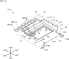
- FIG. 1 is a perspective view showing a semiconductor device according to a first embodiment of the present disclosure.
- FIG. 2 is a perspective view showing the semiconductor device according to the first embodiment of the present disclosure.
- FIG. 3 is a perspective view showing the semiconductor device according to the first embodiment of the present disclosure.
- FIG. 4 is a perspective view of a main part showing the semiconductor device according to the first embodiment of the present disclosure.
- FIG. 5 is a perspective view of a main part showing the semiconductor device according to the first embodiment of the present disclosure.
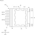
- FIG. 6 is a plan view showing the semiconductor device according to the first embodiment of the present disclosure.
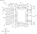
- FIG. 7 is a bottom view showing the semiconductor device according to the first embodiment of the present disclosure.
- FIG. 8 is a front view showing the semiconductor device according to the first embodiment of the present disclosure.
- FIG. 1 is a perspective view showing a semiconductor device according to a first embodiment of the present disclosure.
- FIG. 2 is a perspective view showing the semiconductor device according to the first embodiment of the present disclosure.
- FIG. 9 is a side view showing the semiconductor device according to the first embodiment of the present disclosure.
- FIG. 10 is a plan view of a main portion showing the semiconductor device according to the first embodiment of the present disclosure.
- FIG. 11 is a bottom view of a main portion showing the semiconductor device according to the first embodiment of the present disclosure.
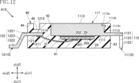
- FIG. 12 is a cross-sectional view taken along line XII-XII in FIG.
- FIG. 13 is a cross-sectional view taken along line XIII-XIII in FIG.
- FIG. 14 is a cross-sectional view taken along line XIV-XIV in FIG.
- FIG. 15 is a cross-sectional view taken along line XV-XV in FIG.
- FIG. 16 is a cross-sectional view showing a state in which the semiconductor device according to the first embodiment of the present disclosure is used.
- FIG. 17 is a schematic diagram of a vehicle including the semiconductor device according to the first embodiment of the present disclosure.
- FIG. 18 is a perspective view showing a semiconductor device according to a first modified example of the first embodiment of the present disclosure.
- FIG. 19 is a perspective view of a main part showing a semiconductor device according to a first modified example of the first embodiment of the present disclosure.
- FIG. 20 is a plan view of a main part showing a semiconductor device according to a first modified example of the first embodiment of the present disclosure.
- FIG. 21 is a perspective view showing a semiconductor device according to a second modification of the first embodiment of the present disclosure.
- FIG. 22 is a perspective view of a main part showing a semiconductor device according to a second modified example of the first embodiment of the present disclosure.
- FIG. 23 is a plan view of a main portion showing a semiconductor device according to a second modification of the first embodiment of the present disclosure.
- FIG. 24 is a bottom view of a main part showing a semiconductor device according to a second modified example of the first embodiment of the present disclosure.
- FIG. 25 is a cross-sectional view taken along line XXV-XXV in FIG.
- FIG. 26 is a cross-sectional view taken along line XXVI-XXVI in FIG.
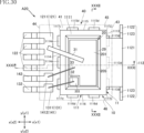
- FIG. 27 is a perspective view showing a semiconductor device according to the second embodiment of the present disclosure.
- FIG. 23 is a plan view of a main portion showing a semiconductor device according to a second modification of the first embodiment of the present disclosure.
- FIG. 24 is a bottom view of a main part showing a semiconductor device according to a second modified example of the first embodiment of the present disclosure
- FIG. 28 is a perspective view of a main part showing a semiconductor device according to a second embodiment of the present disclosure.
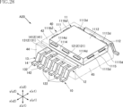
- FIG. 29 is a plan view of a main portion showing a semiconductor device according to a second embodiment of the present disclosure.
- FIG. 30 is a bottom view of a main portion showing a semiconductor device according to a second embodiment of the present disclosure.
- FIG. 31 is a cross-sectional view taken along line XXXI-XXXI in FIG.
- FIG. 32 is a cross-sectional view taken along line XXXII-XXXII in FIG.
- FIG. 33 is a perspective view of a main part of a semiconductor device according to a first modification of the second embodiment.
- FIG. 34 is a plan view of a main portion of a semiconductor device according to a first modification of the second embodiment.
- FIG. FIG. 35 is a cross-sectional view showing a semiconductor device according to a first modification of the second embodiment, and shows a cross section similar to that of FIG.
- FIG. 36 is a cross-sectional view showing a semiconductor device according to a first modification of the second embodiment, and shows a cross section similar to that of FIG.
- an object A is formed on an object B" and “an object A is formed on an object B” include “an object A is formed directly on an object B” and “an object A is formed on an object B with another object interposed between the object A and the object B” unless otherwise specified.
- an object A is disposed on an object B” and “an object A is disposed on an object B” include “an object A is disposed directly on an object B” and “an object A is disposed on an object B with another object interposed between the object A and the object B" unless otherwise specified.
- an object A is located on an object B includes “an object A is located on an object B in contact with an object B” and “an object A is located on an object B with another object interposed between the object A and the object B” unless otherwise specified.
- an object A overlaps an object B when viewed in a certain direction includes “an object A overlaps the entire object B” and “an object A overlaps a part of an object B.”
- a surface A faces in direction B is not limited to the case where the angle of surface A with respect to direction B is 90 degrees, but also includes the case where surface A is tilted with respect to direction B.
- First embodiment: 1 to 16 show a semiconductor device according to a first embodiment of the present disclosure.
- the use of the semiconductor device A10 of this embodiment is not limited in any way, and it is used in electronic devices equipped with a power conversion circuit, such as a DC-DC converter.
- the semiconductor device A10 includes a conductive member 10, a semiconductor element 20, connection members 31, 32, and 33, and a sealing resin 40.
- FIGS. 4 and 5 are perspective views of the main parts of the semiconductor device A10.
- the outer shape of the sealing resin 40 is shown by an imaginary line (two-dot chain line).
- FIG. 6 is a plan view showing the semiconductor device A10.
- FIG. 7 is a bottom view showing the semiconductor device A10.
- FIG. 8 is a front view showing the semiconductor device A10.
- FIG. 9 is a side view showing the semiconductor device A10.
- FIG. 10 is a plan view of the main parts of the semiconductor device A10.
- FIG. 11 is a bottom view of the main parts of the semiconductor device A10.
- the outer shape of the sealing resin 40 is shown by an imaginary line (two-dot chain line).
- FIG. 12 is a cross-sectional view taken along line XII-XII in FIG. 11.
- FIG. 13 is a cross-sectional view taken along line XIII-XIII in FIG. 11.
- FIG. 14 is a cross-sectional view taken along line XIV-XIV in FIG. 11.
- Figure 15 is a cross-sectional view taken along line XV-XV in Figure 11.
- Figure 16 is a cross-sectional view showing the semiconductor device A10 in use.
- an example of a thickness direction in the present disclosure is referred to as the "thickness direction z.”
- An example of a direction perpendicular to the thickness direction z is referred to as the "first direction x.”
- a direction perpendicular to the thickness direction z and the first direction x is referred to as the "second direction y.”
- one side of the thickness direction z is an example of the "one side of the thickness direction” in the present disclosure and is referred to as the "z1 side of the thickness direction z”
- the other side of the thickness direction z is an example of the "other side of the thickness direction” in the present disclosure and is referred to as the "z2 side of the thickness direction z.”
- One side of the first direction x is an example of the "one side of the first direction” in the present disclosure and is referred to as the "x1 side of the first direction x”
- the other side of the first direction x is an example of the "other side of the first direction” in the present disclosure and is
- the conductive member 10 is a member that constitutes a conductive path to the semiconductor element 20.
- the conductive member 10 of this embodiment includes a first lead 11, a second lead 12, a third lead 13, and a fourth lead 14.
- the materials of the first lead 11, the second lead 12, the third lead 13, and the fourth lead 14 are not limited in any way and include, for example, copper (Cu) or a copper alloy.
- the first lead 11, the second lead 12, the third lead 13, and the fourth lead 14 may be plated in appropriate locations with silver (Ag), nickel (Ni), tin (Sn), or the like.
- the first lead 11 has a die pad portion 111 and a first terminal portion 112.
- the die pad portion 111 has a first main surface 1111 and a first back surface 1112.
- the first main surface 1111 is a surface facing the z1 side in the thickness direction z.
- the first back surface 1112 is a surface facing the z2 side in the thickness direction z.
- a semiconductor element 20 is mounted on the first main surface 1111.
- the die pad portion 111 has a first side surface 1113, a second side surface 1114, a third side surface 1115 and a fourth side surface 1116.
- Each of the first side surface 1113, the second side surface 1114, the third side surface 1115 and the fourth side surface 1116 is located between the first main surface 1111 and the first back surface 1112 in the thickness direction z.
- the first side surface 1113 and the second side surface 1114 are spaced apart in the first direction x.
- the first side surface 1113 is located on the x1 side of the first direction x and is a surface facing the x1 side of the first direction x.
- the second side surface 1114 is located on the x2 side of the first direction x and is a surface facing the x2 side of the first direction x.
- the third side surface 1115 and the fourth side surface 1116 are spaced apart in the second direction y.
- the third side surface 1115 is located on the y1 side in the second direction y and faces the y1 side in the second direction y.
- the fourth side surface 1116 is located on the y2 side in the second direction y and faces the y2 side in the second direction y.
- the die pad portion 111 further has a first corner 1117a, a second corner 1117b, a third corner 1117c, and a fourth corner 1117d.
- the first corner 1117a is the portion where the first side surface 1113 and the third side surface 1115 meet.
- the second corner 1117b is the portion where the first side surface 1113 and the fourth side surface 1116 meet.
- the third corner 1117c is the portion where the second side surface 1114 and the third side surface 1115 meet.
- the fourth corner 1117d is the portion where the second side surface 1114 and the fourth side surface 1116 meet.
- the die pad portion 111 has a plurality of first recesses 1113a, a plurality of second recesses 1114a, a plurality of third recesses 1115a, and a plurality of fourth recesses 1116a.
- the multiple first recesses 1113a are recessed from the first back surface 1112 and the first side surface 1113.
- the multiple first recesses 1113a are arranged at intervals in the second direction y.
- three first recesses 1113a are provided in the die pad portion 111.
- the three first recesses 1113a are arranged at regular intervals in the second direction y.
- the interval (first dimension L1) between two adjacent first recesses 1113a in the second direction y is 1/5 to 5 times the length (second dimension L2) of the first recesses 1113a in the second direction y.
- the interval (first dimension L1) between two adjacent first recesses 1113a is approximately 1.0 times the length (second dimension L2) of the first recesses 1113a.
- Each of the multiple first recesses 1113a has a first intermediate surface 1113b.
- the first intermediate surface 1113b is located between the first main surface 1111 and the first back surface 1112 in the thickness direction z, and faces the z2 side in the thickness direction z (the same side as the first back surface 1112).
- the second recesses 1114a are recessed from the first back surface 1112 and the second side surface 1114.
- the second recesses 1114a are arranged at intervals in the second direction y.
- the die pad portion 111 has three second recesses 1114a.
- the three second recesses 1114a are arranged at regular intervals in the second direction y.
- the interval (third dimension L3) between two adjacent second recesses 1114a in the second direction y is 1/5 to 5 times the length (fourth dimension L4) of the second recesses 1114a in the second direction y.
- the interval (third dimension L3) between two adjacent second recesses 1114a is approximately 1.0 times the length (fourth dimension L4) of the second recesses 1114a.
- Each of the multiple second recesses 1114a has a second intermediate surface 1114b.
- the second intermediate surface 1114b is located between the first main surface 1111 and the first back surface 1112 in the thickness direction z, and faces the z2 side in the thickness direction z (the same side as the first back surface 1112).
- the multiple third recesses 1115a are recessed from the first back surface 1112 and the third side surface 1115.
- the multiple third recesses 1115a are arranged at intervals in the first direction x.
- two third recesses 1115a are provided in the die pad portion 111.
- the interval (fifth dimension L5) between two adjacent third recesses 1115a in the first direction x is 1/5 to 5 times the length (sixth dimension L6) of the third recesses 1115a in the first direction x.
- the interval (fifth dimension L5) between two adjacent third recesses 1115a is approximately 1.0 times the length (sixth dimension L6) of the third recesses 1115a.
- Each of the multiple third recesses 1115a has a third intermediate surface 1115b.
- the third intermediate surface 1115b is located between the first main surface 1111 and the first back surface 1112 in the thickness direction z, and faces the z2 side in the thickness direction z (the same side as the first back surface 1112).
- the multiple fourth recesses 1116a are recessed from the first back surface 1112 and the fourth side surface 1116.
- the multiple fourth recesses 1116a are arranged at intervals in the first direction x.
- two fourth recesses 1116a are provided in the die pad portion 111.
- the interval (seventh dimension L7) between two adjacent fourth recesses 1116a in the first direction x is 1/5 to 5 times the length (eighth dimension L8) of the fourth recess 1116a in the first direction x.
- the interval (seventh dimension L7) between two adjacent fourth recesses 1116a is approximately 1.0 times the length (eighth dimension L8) of the fourth recess 1116a.
- Each of the multiple fourth recesses 1116a has a fourth intermediate surface 1116b.
- the fourth intermediate surface 1116b is located between the first main surface 1111 and the first back surface 1112 in the thickness direction z, and faces the z2 side in the thickness direction z (the same side as the first back surface 1112).
- the multiple first recesses 1113a are provided at positions that avoid both ends of the first side surface 1113 in the second direction y. As a result, each of the multiple first recesses 1113a does not contact either the first corner portion 1117a or the second corner portion 1117b. Also, the multiple second recesses 1114a are provided at positions that avoid both ends of the second side surface 1114 in the second direction y. As a result, each of the multiple second recesses 1114a does not contact either the third corner portion 1117c or the fourth corner portion 1117d.
- the multiple third recesses 1115a are provided at positions that avoid both ends of the third side surface 1115 in the first direction x.
- each of the multiple third recesses 1115a does not contact either the first corner portion 1117a or the third corner portion 1117c.
- the multiple fourth recesses 1116a are provided at positions that avoid both ends of the fourth side surface 1116 in the first direction x. As a result, each of the multiple fourth recesses 1116a is not in contact with either the second corner 1117b or the fourth corner 1117d.
- the die pad portion 111 has a plurality of first protrusions 1113c, a plurality of second protrusions 1114c, a plurality of third protrusions 1115c, and a plurality of fourth protrusions 1116c.
- the first protrusions 1113c are individually connected to the first recesses 1113a. Each of the first protrusions 1113c protrudes from the first side surface 1113 to the x1 side in the first direction x.
- the second protrusions 1114c are individually connected to the second recesses 1114a. Each of the second protrusions 1114c protrudes from the second side surface 1114 to the x2 side in the first direction x.
- the third protrusions 1115c are individually connected to the third recesses 1115a. Each of the third protrusions 1115c protrudes from the third side surface 1115 to the y1 side in the second direction y.
- the fourth protrusions 1116c are individually connected to the fourth recesses 1116a. Each of the fourth protrusions 1116c protrudes from the fourth side surface 1116 to the y2 side in the second direction y.
- the multiple first recesses 1113a to 4th recesses 1116a and multiple first protrusions 1113c to 4th protrusions 1116c in the above configuration are formed, for example, by pressing the first back surface 1112 of the die pad portion 111 in appropriate positions toward the z1 side in the thickness direction z.
- the multiple first recesses 1113a to 4th recesses 1116a and multiple first protrusions 1113c to 4th protrusions 1116c are covered with and in contact with the sealing resin 40 described below.
- the first terminal portion 112 has a first portion 1121, two second portions 1122, and two third portions 1123.
- the first portion 1121 is connected to the die pad portion 111 and extends from the die pad portion 111 to the x1 side in the first direction x, and in the illustrated example, is parallel (or approximately parallel) to the xy plane.
- the die pad portion 111 has a larger size in the thickness direction z than the first portion 1121.
- the first terminal portion 112 in this embodiment has only one first portion 1121.
- the shape of the first portion 1121 is not limited in any way, and in the illustrated example, it is rectangular when viewed in the thickness direction z.
- the first portion 1121 is separated from the first back surface 1112 in the thickness direction z, and in the illustrated example, it is in contact with the first main surface 1111. One side of the first portion 1121 is flush with the first main surface 1111.
- the two second parts 1122 are located on the z1 side of the first part 1121 in the thickness direction z.
- the two second parts 1122 are used when surface mounting the semiconductor device A10 on a circuit board or the like.
- the two third portions 1123 are interposed between the first portion 1121 and the two second portions 1122.
- the third portions 1123 extend from the first portion 1121 toward the z1 side in the thickness direction z.
- the third portions 1123 are inclined with respect to the thickness direction z so as to extend outward from the first portion 1121 in the second direction y.
- the shape of the third portions 1123 is not limited in any way, and in the illustrated example, they are rectangular when viewed in the first direction x.
- the two second portions 1122 extend outward in the second direction y from the two third portions 1123.
- the two second portions 1122 are parallel (or approximately parallel) to the second direction y.
- the two second portions 1122 do not extend beyond the two third portions 1123 to the x1 side in the first direction x.
- the two second portions 1122 and the two third portions 1123 are at the same (or approximately the same) position in the first direction x.
- the second lead 12 is located away from the first lead 11 (die pad portion 111) on the x2 side in the first direction x.
- the second lead 12 has a pad portion 121 and a plurality of second terminal portions 122.
- the pad portion 121 has a second main surface 1211 and a second back surface 1212.
- the second main surface 1211 faces the z1 side in the thickness direction z.
- the second back surface 1212 faces the z2 side in the thickness direction z.
- the connection member 31 is connected to the second main surface 1211.
- the shape of the pad portion 121 is not limited in any way, and in the illustrated example, it is an elongated rectangle with the second direction y as the longitudinal direction.
- the pad portion 121 when viewed in the thickness direction z, the pad portion 121 is smaller than the die pad portion 111.
- the pad portion 121 is smaller in size in the thickness direction z than the die pad portion 111 and is the same (or approximately the same) as the first terminal portion 112.
- the position of the second main surface 1211 in the thickness direction z is the same (or approximately the same) as the first main surface 1111 of the die pad portion 111.
- the second terminal portions 122 are arranged side by side in the second direction y.
- the second terminal portions 122 have a fourth portion 1221, a fifth portion 1222, and a sixth portion 1223.
- the fourth portion 1221 is connected to the pad portion 121 and extends from the pad portion 121 to the x2 side in the first direction x, and in the illustrated example is parallel (or approximately parallel) to the xy plane.
- the shape of the fourth portion 1221 is not limited in any way, and in the illustrated example, it is rectangular when viewed in the thickness direction z.
- the fifth portion 1222 is located on the z1 side of the fourth portion 1221 in the thickness direction z.
- the fifth portion 1222 is used when surface-mounting the semiconductor device A10 on a circuit board or the like.
- the fifth portion 1222 has a shape that extends along the first direction x.
- the sixth portion 1223 is interposed between the fourth portion 1221 and the fifth portion 1222.
- the sixth portion 1223 extends from the fourth portion 1221 toward the z1 side in the thickness direction z.
- the sixth portion 1223 is inclined with respect to the thickness direction z (yz plane).
- the shape of the sixth portion 1223 is not limited in any way, and in the illustrated example, it is rectangular when viewed in the first direction x.
- the third lead 13 is located away from the first lead 11 (die pad portion 111) on the x2 side in the first direction x.
- the third lead 13 is also aligned with the second lead 12 in the second direction y.
- the third lead 13 has a pad portion 131 and a third terminal portion 132.
- the pad portion 131 has a third main surface 1311 and a third back surface 1312.
- the third main surface 1311 is a surface facing the z1 side in the thickness direction z.
- the third back surface 1312 is a surface facing the z2 side in the thickness direction z.
- the connection member 32 is connected to the third main surface 1311.
- the shape of the pad portion 131 is not limited in any way, and in the illustrated example, it is rectangular when viewed in the thickness direction z. Also, when viewed in the thickness direction z, the pad portion 131 is smaller than the pad portion 121. Also, the size of the pad portion 131 in the thickness direction z is smaller than that of the die pad portion 111, and is the same (or approximately the same) as the pad portion 121. In the illustrated example, the position of the third main surface 1311 in the thickness direction z is the same (or approximately the same) as that of the first main surface 1111 of the die pad portion 111.
- the third terminal portion 132 has a seventh portion 1321, an eighth portion 1322, and a ninth portion 1323.
- the seventh portion 1321 is connected to the pad portion 131 and extends from the pad portion 131 to the x2 side in the first direction x, and in the illustrated example is parallel (or approximately parallel) to the xy plane.
- the shape of the seventh portion 1321 is not limited in any way, and in the illustrated example, it is rectangular when viewed in the thickness direction z.
- the eighth portion 1322 is located on the z1 side of the seventh portion 1321 in the thickness direction z.
- the eighth portion 1322 is used when surface-mounting the semiconductor device A10 on a circuit board or the like.
- the eighth portion 1322 has a shape that extends along the first direction x.
- the ninth portion 1323 is interposed between the seventh portion 1321 and the eighth portion 1322.
- the ninth portion 1323 extends from the seventh portion 1321 toward the z1 side in the thickness direction z.
- the ninth portion 1323 is inclined with respect to the thickness direction z (yz plane).
- the shape of the ninth portion 1323 is not limited in any way, and in the illustrated example, it is rectangular when viewed in the first direction x.
- the fourth lead 14 is located away from the first lead 11 (die pad portion 111) on the other side in the x direction.
- the fourth lead 14 is also located between the second lead 12 and the third lead 13 in the y direction.
- the fourth lead 14 has a pad portion 141 and a fourth terminal portion 142.
- the pad portion 141 has a fourth main surface 1411 and a fourth back surface 1412.
- the fourth main surface 1411 is a surface facing the z1 side in the thickness direction z.
- the fourth back surface 1412 is a surface facing the z2 side in the thickness direction z.
- the connection member 33 is connected to the fourth main surface 1411.
- the shape of the pad portion 141 is not limited in any way, and in the illustrated example, it is rectangular when viewed in the thickness direction z. Also, when viewed in the thickness direction z, the pad portion 141 is smaller than the pad portion 121 and is about the same size as the pad portion 131.
- the pad portion 141 is smaller in size in the thickness direction z than the die pad portion 111 and is the same (or approximately the same) as the pad portion 121 and the pad portion 131.
- the position of the fourth main surface 1411 in the thickness direction z is the same (or approximately the same) as the first main surface 1111 of the die pad portion 111.
- the fourth terminal portion 142 has a tenth portion 1421, an eleventh portion 1422, and a twelfth portion 1423.
- the tenth portion 1421 is connected to the pad portion 141 and extends from the pad portion 141 to the x2 side in the first direction x, and in the illustrated example is parallel (or approximately parallel) to the xy plane.
- the shape of the tenth portion 1421 is not limited in any way, and in the illustrated example, it is rectangular when viewed in the thickness direction z.
- the 11th portion 1422 is located on the z1 side of the 10th portion 1421 in the thickness direction z.
- the 11th portion 1422 is used when surface-mounting the semiconductor device A10 on a circuit board or the like.
- the 11th portion 1422 has a shape that extends along the first direction x.
- the twelfth portion 1423 is interposed between the tenth portion 1421 and the eleventh portion 1422.
- the twelfth portion 1423 extends from the tenth portion 1421 toward the z1 side in the thickness direction z.
- the twelfth portion 1423 is inclined with respect to the thickness direction z (yz plane).
- the shape of the twelfth portion 1423 is not limited in any way, and in the illustrated example, it is rectangular when viewed in the first direction x.
- the semiconductor element 20 is mounted on the first main surface 1111 of the die pad portion 111, as shown in Figures 5 and 11 to 15.
- the semiconductor element 20 is an n-channel type MOSFET (Metal-Oxide-Semiconductor Field-Effect Transistor) with a vertical structure.
- the semiconductor element 20 is not limited to a MOSFET.
- the semiconductor element 20 may be other transistors such as an IGBT (Insulated Gate Bipolar Transistor).
- the semiconductor element 20 may be a diode.
- the semiconductor element 20 is rectangular when viewed in the thickness direction z.
- the semiconductor element 20 When viewed in the thickness direction z, the semiconductor element 20 does not overlap any of the multiple first recesses 1113a, the multiple second recesses 1114a, the multiple third recesses 1115a, or the multiple fourth recesses 1116a.
- the semiconductor element 20 has a semiconductor layer 205, a first electrode 201, a second electrode 202, and a third electrode 203.
- the semiconductor layer 205 includes a compound semiconductor substrate.
- the main material of the compound semiconductor substrate is silicon carbide (SiC).
- silicon (Si) may be used as the main material of the compound semiconductor substrate.
- the first electrode 201 is provided on a portion of the semiconductor layer 205 on the side (z1 side) facing the first main surface 1111 of the die pad portion 111 of the first lead 11 in the thickness direction z.
- the first electrode 201 corresponds to the source electrode of the semiconductor element 20.
- the second electrode 202 is provided on a portion of the semiconductor layer 205 opposite the first electrode 201 in the thickness direction z.
- the second electrode 202 faces the first main surface 1111 of the die pad portion 111 of the first lead 11.
- the second electrode 202 corresponds to the drain electrode of the semiconductor element 20.
- the second electrode 202 is conductively joined to the first main surface 1111 via a joining layer 29.
- the joining layer 29 is, for example, a conductive joining material such as solder, silver (Ag) paste, or baked silver.
- the third electrode 203 is provided in a portion of the semiconductor layer 205 on the same side as the first electrode 201 in the thickness direction z (the z1 side in the thickness direction z), and is located away from the first electrode 201.
- the third electrode 203 corresponds to the gate electrode of the semiconductor element 20. When viewed in the thickness direction z, the area of the third electrode 203 is smaller than the area of the first electrode 201.
- connection member 31 is bonded to the first electrode 201 of the semiconductor element 20 and the second main surface 1211 of the pad portion 121 of the second lead 12.
- material of the connection member 31 includes metals such as aluminum (Al), copper (Cu), and gold (Au).
- connection member 31 contains aluminum (Al) and is a flat, band-shaped member.
- connection member 32 is connected to the third electrode 203 of the semiconductor element 20 and the third main surface 1311 of the pad portion 131 of the third lead 13.
- the connection member 32 contains gold (Au) and is a linear member that is thinner than the connection member 31.
- connection member 33 is connected to the first electrode 201 of the semiconductor element 20 and the fourth main surface 1411 of the pad portion 141 of the fourth lead 14.
- the connection member 33 contains gold (Au) and is a linear member that is thinner than the connection member 31.
- the first terminal portion 112 of the first lead 11 is a drain terminal
- the second terminal portion 122 of the second lead 12 is a source terminal
- the third terminal portion 132 of the third lead 13 is a gate terminal
- the fourth terminal portion 142 of the fourth lead 14 is a source sense terminal.
- the sealing resin 40 covers the semiconductor element 20, the connection members 31, 32, 33, and parts of each of the first lead 11, the second lead 12, the third lead 13, and the fourth lead 14.
- the sealing resin 40 has electrical insulation properties.
- the sealing resin 40 is made of a material that contains, for example, black epoxy resin.
- the sealing resin 40 has a first resin surface 41, a second resin surface 42, a third resin surface 43, a fourth resin surface 44, a fifth resin surface 45, and a sixth resin surface 46.
- the first resin surface 41 faces the same side (z1 side) as the first main surface 1111 of the die pad portion 111 of the first lead 11 in the thickness direction z.
- the second resin surface 42 faces the opposite side (z2 side) to the first resin surface 41 in the thickness direction z.
- the first back surface 1112 of the die pad portion 111 of the first lead 11 is exposed from the second resin surface 42.
- the second resin surface 42 and the first back surface 1112 are flush with each other.
- the first back surface 1112 is separated from the third resin surface 43 in the first direction x.
- the third resin surface 43 faces the x1 side in the first direction x.
- the first portion 1121 of the first terminal portion 112 of the first lead 11 penetrates the third resin surface 43.
- only one first portion 1121 penetrates the third resin surface 43.
- the first portion 1121 is separated from the second resin surface 42 in the thickness direction z.
- the fourth resin surface 44 faces the opposite side to the third resin surface 43 in the first direction x (the x2 side in the first direction x).
- the second terminal portions 122 of the multiple second terminal portions 122 of the second lead 12, the seventh portion 1321 of the third terminal portion 132 of the third lead 13, and the tenth portion 1421 of the fourth terminal portion 142 of the fourth lead 14 penetrate the fourth resin surface 44.
- the fifth resin surface 45 and the sixth resin surface 46 face in opposite directions in the second direction y.
- the second direction y ends of the two second portions 1122 of the second terminal portion 122 of the first lead 11 are located at approximately the same position in the y direction as the fifth resin surface 45 and the sixth resin surface 46 of the sealing resin 40.
- the two second portions 1122 do not protrude from the fifth resin surface 45 and the sixth resin surface 46 in the second direction y.
- the sealing resin 40 has a groove 49.
- the groove 49 is recessed from the second resin surface 42 in the first direction x and extends along the second direction y.
- the groove 49 reaches the fifth resin surface 45 and the sixth resin surface 46.
- the groove 49 is located between the first back surface 1112 and the fourth resin surface 44.
- FIG. 16 shows the semiconductor device A10 in use.
- the semiconductor device A10 is surface-mounted on a circuit board 92. That is, the second portion 1122 of the first terminal portion 112, the fifth portion 1222 of the second terminal portion 122, the eighth portion 1322 of the third terminal portion 132, and the eleventh portion 1422 of the fourth terminal portion 142 are conductively joined to the wiring pattern (not shown) of the circuit board 92 by, for example, solder 921.
- a heat sink 91 is disposed opposite the first back surface 1112 of the die pad portion 111.
- a sheet material 919 is disposed between the first back surface 1112 and the heat sink 91.
- the sheet material 919 is, for example, an insulating sheet.
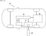
- FIG. 17 is a schematic diagram of a vehicle B1 equipped with a semiconductor device A10.
- the vehicle B1 is, for example, an electric vehicle (EV).
- the vehicle B1 is equipped with a drive system 84 including an AC-DC conversion device 81, a power receiving device 82, and a storage battery 83.
- the semiconductor device A10 constitutes a part of the AC-DC conversion device 81.
- the AC-DC conversion device 81 converts the AC power into high-voltage DC power.
- the AC-DC conversion device 81 supplies the high-voltage DC power to the storage battery 83.
- the power receiving device 82 supplies power to the storage battery 83 by a non-contact charging system, and is supplied with power by an electromagnetic induction method from a non-contact charger (not shown) installed in a parking lot or the like.
- the power stored in the storage battery 83 is supplied to a drive system 84 consisting of an inverter, an AC motor, and a transmission.
- the drive system 84 drives the vehicle B1.
- the above AC-DC conversion device 81 is an example of a "power conversion device" of this disclosure.
- the die pad portion 111 on which the semiconductor element 20 is mounted has a first back surface 1112 facing the z2 side in the thickness direction z and a first side surface 1113 facing the x1 side in the first direction x.
- the first back surface 1112 is exposed from the sealing resin 40.
- the die pad portion 111 also has a plurality of first recesses 1113a. Each of the plurality of first recesses 1113a is recessed from the first back surface 1112 and the first side surface 1113.
- the plurality of first recesses 1113a are arranged at intervals in the second direction y.
- the contact area between the die pad portion 111 on which the semiconductor element 20 is mounted and the sealing resin 40 is efficiently increased, and the adhesion between the die pad portion 111 and the sealing resin 40 can be improved.
- the distance (first dimension L1) between two adjacent first recesses 1113a in the second direction y is 1/5 to 5 times the length (second dimension L2) of the first recesses 1113a in the second direction y.
- the die pad portion 111 further has a plurality of second recesses 1114a, a plurality of third recesses 1115a, and a plurality of fourth recesses 1116a.
- Each of the plurality of second recesses 1114a is recessed from the first back surface 1112 and the second side surface 1114.
- the plurality of second recesses 1114a are arranged at intervals in the second direction y.
- Each of the plurality of third recesses 1115a is recessed from the first back surface 1112 and the third side surface 1115.
- the plurality of third recesses 1115a are arranged at intervals in the first direction x.
- Each of the plurality of fourth recesses 1116a is recessed from the first back surface 1112 and the fourth side surface 1116.
- the plurality of fourth recesses 1116a are arranged at intervals in the first direction x.
- the contact area between the die pad portion 111 on which the semiconductor element 20 is mounted and the sealing resin 40 can be increased more efficiently, and the adhesion between the die pad portion 111 and the sealing resin 40 can be further improved.
- the distance (third dimension L3) between two adjacent second recesses 1114a in the second direction y is 1/5 to 5 times the length (fourth dimension L4) of the second recesses 1114a in the second direction y.
- the distance (fifth dimension L5) between two adjacent third recesses 1115a in the first direction x is 1/5 to 5 times the length (sixth dimension L6) of the third recesses 1115a in the first direction x.
- the distance (seventh dimension L7) between two adjacent fourth recesses 1116a in the first direction x is 1/5 to 5 times the length (eighth dimension L8) of the fourth recess 1116a in the first direction x. This makes it possible to appropriately prevent the peeling of the sealing resin 40 from progressing even if partial peeling occurs in the sealing resin 40 that contacts the third recess 1115a and the fourth recess 1116a.
- Each of the first recesses 1113a is not in contact with either the first corner 1117a or the second corner 1117b.
- each of the second recesses 1114a is not in contact with either the third corner 1117c or the fourth corner 1117d.
- Each of the third recesses 1115a is not in contact with either the first corner 1117a or the third corner 1117c.
- Each of the fourth recesses 1116a is not in contact with either the second corner 1117b or the fourth corner 1117d.
- the semiconductor element 20 does not overlap any of the first recesses 1113a, the second recesses 1114a, the third recesses 1115a, or the fourth recesses 1116a in the thickness direction z.
- the flatness of the portion of the first main surface 1111 opposite the pressed surface that overlaps with the first recesses 1113a to the fourth recesses 1116a in the thickness direction z may decrease.
- the semiconductor element 20 is positioned in a position that does not overlap with the first recesses 1113a to the fourth recesses 1116a in the thickness direction z, so that a good bonding state with the first main surface 1111 can be maintained.
- FIGS. 18 to 36 show modified examples and other embodiments of the semiconductor device of the present disclosure.
- elements that are the same as or similar to those in the above-described embodiment are given the same reference numerals as in the above-described embodiment, and redundant explanations will be omitted.
- the configurations of the various parts in each modified example and each embodiment can be combined with each other as appropriate to the extent that no technical contradictions arise.
- FIG. 18 to 20 show a first modified example of the semiconductor device A10.
- FIG. 18 is a perspective view showing a semiconductor device A11 according to the first modified example.
- FIG. 19 is a perspective view showing a main part of the semiconductor device A11.
- FIG. 20 is a plan view showing a main part of the semiconductor device A11.
- the outline of the sealing resin 40 is shown by an imaginary line (two-dot chain line).
- the semiconductor device A11 of this modified example differs from the semiconductor device A10 in the arrangement of the first recess 1113a, the second recess 1114a, the third recess 1115a, and the fourth recess 1116a in the die pad portion 111.
- the number of first recesses 1113a, second recesses 1114a, third recesses 1115a, and fourth recesses 1116a formed in the die pad portion 111 is greater than that of the semiconductor device A10.
- the die pad portion 111 is provided with five first recesses 1113a, five second recesses 1114a, three third recesses 1115a, and three fourth recesses 1116a.
- the five first recesses 1113a are arranged at regular intervals in the second direction y.
- the interval (first dimension L1) between two adjacent first recesses 1113a in the second direction y is 1/5 to 5 times the length (second dimension L2) of the first recesses 1113a in the second direction y.
- the interval (first dimension L1) between two adjacent first recesses 1113a is approximately 0.63 times the length (second dimension L2) of the first recess 1113a.
- the five second recesses 1114a are arranged at regular intervals in the second direction y.
- the interval (third dimension L3) between two adjacent second recesses 1114a in the second direction y is 1/5 to 5 times the length (fourth dimension L4) of the second recess 1114a in the second direction y.
- the interval (third dimension L3) between the two second recesses 1114a is about 0.63 times the length (fourth dimension L4) of the second recesses 1114a.
- the three third recesses 1115a are arranged at regular intervals in the first direction x.
- the interval (fifth dimension L5) between two adjacent third recesses 1115a in the first direction x is 1/5 to 5 times the length (sixth dimension L6) of the third recesses 1115a in the first direction x.
- the interval (fifth dimension L5) between two adjacent third recesses 1115a is about 0.93 times the length (sixth dimension L6) of the third recesses 1115a.
- the three fourth recesses 1116a are arranged at regular intervals in the first direction x.
- the distance (seventh dimension L7) between two adjacent fourth recesses 1116a in the first direction x is 1/5 to 5 times the length (eighth dimension L8) of the fourth recesses 1116a in the first direction x.
- the distance (seventh dimension L7) between two adjacent fourth recesses 1116a is approximately 0.93 times the length (eighth dimension L8) of the fourth recesses 1116a.
- the die pad portion 111 on which the semiconductor element 20 is mounted has a plurality of first recesses 1113a.
- Each of the plurality of first recesses 1113a is recessed from the first back surface 1112 and the first side surface 1113.
- the plurality of first recesses 1113a are arranged at intervals in the second direction y.
- the distance (first dimension L1) between two adjacent first recesses 1113a in the second direction y is 1/5 to 5 times the length (second dimension L2) of the first recesses 1113a in the second direction y.
- the number of first recesses 1113a, second recesses 1114a, third recesses 1115a, and fourth recesses 1116a formed in the die pad portion 111 is greater than that of the semiconductor device A10.
- the contact area between the die pad portion 111 and the sealing resin 40 can be further increased. This is more preferable in terms of improving the adhesion between the die pad portion 111 and the sealing resin 40.
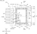
- FIG. 21 to 26 show a second modified example of the semiconductor device A10.
- FIG. 21 is a perspective view showing a semiconductor device A12 according to the second modified example.
- FIG. 22 is a perspective view showing a main part of the semiconductor device A12.
- FIG. 23 is a plan view showing a main part of the semiconductor device A12.
- FIG. 24 is a bottom view showing a main part of the semiconductor device A12.
- the outer shape of the sealing resin 40 is shown by an imaginary line (two-dot chain line).
- FIG. 25 is a cross-sectional view taken along line XXV-XXV in FIG. 24.
- FIG. 26 is a cross-sectional view taken along line XXVI-XXVI in FIG.
- the semiconductor device A12 of this modified example is different from the semiconductor device A10 in the configurations of the first recess 1113a, the second recess 1114a, the third recess 1115a, and the fourth recess 1116a in the die pad portion 111, and in the arrangement of the semiconductor element 20.
- the length in the thickness direction z of the first recess 1113a (the distance in the thickness direction z between the first back surface 1112 and the first intermediate surface 1113b) is greater than that of the semiconductor device A10.
- the length in the thickness direction z of each of the second recess 1114a, the third recess 1115a, and the fourth recess 1116a is greater than that of the semiconductor device A10.
- the length in the first direction x of the first recess 1113a is greater than that of the semiconductor device A10.
- the length in the first direction x of the second recess 1114a is greater than that of the semiconductor device A10, and the length in the second direction y of each of the third recess 1115a and the fourth recess 1116a is greater than that of the semiconductor device A10.
- the first dimension L1 to the eighth dimension L8 described in the semiconductor device A10 are the same (or approximately the same) dimensions in the semiconductor device A12 as those in the semiconductor device A10.
- the die pad portion 111 does not have the first protrusion 1113c, the second protrusion 1114c, the third protrusion 1115c, and the fourth protrusion 1116c.
- the first recesses 1113a, the second recesses 1114a, the third recesses 1115a, and the fourth recesses 1116a of this modified example are formed by a chemical process such as etching.
- the size of the semiconductor element 20 in a plan view is larger than that of the semiconductor device A10.
- the semiconductor element 20 overlaps with a portion of each of the multiple first recesses 1113a, the multiple second recesses 1114a, the multiple third recesses 1115a, and the multiple fourth recesses 1116a.
- the die pad portion 111 on which the semiconductor element 20 is mounted has a plurality of first recesses 1113a.
- Each of the plurality of first recesses 1113a is recessed from the first back surface 1112 and the first side surface 1113.
- the plurality of first recesses 1113a are arranged at intervals in the second direction y.
- the distance (first dimension L1) between two adjacent first recesses 1113a in the second direction y is 1/5 to 5 times the length (second dimension L2) of the first recesses 1113a in the second direction y.
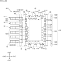
- FIG. 27 to 32 show a semiconductor device according to the second embodiment of the present disclosure.
- FIG. 27 is a perspective view showing the semiconductor device A20 according to the present embodiment.
- FIG. 28 is a perspective view showing a main part of the semiconductor device A20.
- FIG. 29 is a plan view showing a main part of the semiconductor device A20.
- FIG. 30 is a bottom view showing a main part of the semiconductor device A20.
- the outer shape of the sealing resin 40 is shown by an imaginary line (two-dot chain line).
- FIG. 31 is a cross-sectional view taken along line XXXI-XXXI in FIG. 30.
- FIG. 32 is a cross-sectional view taken along line XXXII-XXXII in FIG.
- the semiconductor device A20 of this embodiment differs from the semiconductor device A10 in the configuration of the die pad portion 111.
- the die pad portion 111 has a plurality of fifth protrusions 1113d, a plurality of sixth protrusions 1114d, a plurality of seventh protrusions 1115d, and a plurality of eighth protrusions 1116d.
- the die pad portion 111 does not have the first recess 1113a, the second recess 1114a, the third recess 1115a, or the fourth recess 1116a.
- the multiple fifth protrusions 1113d each protrude from the first side surface 1113 toward the x1 side in the first direction x.
- the multiple fifth protrusions 1113d are located toward the z2 side in the thickness direction z of the first side surface 1113.
- the multiple fifth protrusions 1113d are arranged at intervals in the second direction y.
- the die pad portion 111 is provided with three fifth protrusions 1113d.
- the three fifth protrusions 1113d are lined up at regular intervals in the second direction y.
- Each of the multiple fifth protrusions 1113d has a fifth intermediate surface 1113e.
- the fifth intermediate surface 1113e is located between the first main surface 1111 and the first back surface 1112 in the thickness direction z, and faces the z2 side in the thickness direction z (the same side as the first back surface 1112).
- the multiple sixth protrusions 1114d each protrude from the second side surface 1114 toward the x2 side in the first direction x.
- the multiple sixth protrusions 1114d are located toward the z2 side in the thickness direction z of the second side surface 1114.
- the multiple sixth protrusions 1114d are arranged at intervals in the second direction y.
- the die pad portion 111 has three sixth protrusions 1114d.
- the three sixth protrusions 1114d are arranged at regular intervals in the second direction y.
- Each of the sixth protrusions 1114d has a sixth intermediate surface 1114e.
- the sixth intermediate surface 1114e is located between the first main surface 1111 and the first back surface 1112 in the thickness direction z, and faces the z2 side in the thickness direction z (the same side as the first back surface 1112).
- the multiple seventh protrusions 1115d each protrude from the third side surface 1115 toward the y1 side in the second direction y.
- the multiple seventh protrusions 1115d are located toward the z2 side in the thickness direction z of the third side surface 1115.
- the multiple seventh protrusions 1115d are arranged at intervals in the first direction x.
- the die pad portion 111 is provided with two seventh protrusions 1115d.
- Each of the seventh protrusions 1115d has a seventh intermediate surface 1115e.
- the seventh intermediate surface 1115e is located between the first main surface 1111 and the first back surface 1112 in the thickness direction z, and faces the z2 side in the thickness direction z (the same side as the first back surface 1112).
- the multiple eighth protrusions 1116d each protrude from the fourth side surface 1116 toward the y2 side in the second direction y.
- the multiple eighth protrusions 1116d are located toward the z2 side in the thickness direction z of the fourth side surface 1116.
- the multiple eighth protrusions 1116d are arranged at intervals in the first direction x.
- the die pad portion 111 is provided with two eighth protrusions 1116d.
- Each of the multiple eighth protrusions 1116d has an eighth intermediate surface 1116e.
- the eighth intermediate surface 1116e is located between the first main surface 1111 and the first back surface 1112 in the thickness direction z, and faces the z2 side in the thickness direction z (the same side as the first back surface 1112).
- the multiple fifth protrusions 1113d are provided at positions that avoid both ends of the first side surface 1113 in the second direction y. As a result, each of the multiple fifth protrusions 1113d does not contact either the first corner portion 1117a or the second corner portion 1117b.
- the multiple sixth protrusions 1114d are provided at positions that avoid both ends of the second side surface 1114 in the second direction y. As a result, each of the multiple sixth protrusions 1114d does not contact either the third corner portion 1117c or the fourth corner portion 1117d.
- the multiple seventh protrusions 1115d are provided at positions that avoid both ends of the third side surface 1115 in the first direction x.
- each of the multiple seventh protrusions 1115d does not contact either the first corner portion 1117a or the third corner portion 1117c.
- the eighth protrusions 1116d are provided at positions that avoid both ends of the fourth side surface 1116 in the first direction x. As a result, each of the eighth protrusions 1116d is not in contact with either the second corner 1117b or the fourth corner 1117d.
- the plurality of fifth to eighth protrusions 1113d to 1116d in the above configuration are formed, for example, by pressing from the first back surface 1112 side of the die pad portion 111 toward the z1 side in the thickness direction z.
- the die pad portion 111 before pressing has protrusions corresponding to the plurality of fifth to eighth protrusions 1113d to 1116d.
- Each protrusion is connected to the first back surface 1112 and protrudes from a corresponding one of the first to fourth side surfaces 1113 to 1116.
- each protrusion is pressed along the boundary line of the first back surface 1112.
- the fifth to eighth protrusions 1113d to 1116d are formed with the fifth to eighth intermediate surfaces 1113e to 1116e. All of the multiple fifth protrusions 1113d to eighth protrusions 1116d are covered with and in contact with the sealing resin 40.
- the die pad portion 111 on which the semiconductor element 20 is mounted has a plurality of fifth protrusions 1113d.
- Each of the plurality of fifth protrusions 1113d protrudes from the first side surface 1113 toward the x1 side in the first direction x.
- the plurality of fifth protrusions 1113d are arranged at intervals in the second direction y.
- the die pad portion 111 further has a plurality of sixth protrusions 1114d, a plurality of seventh protrusions 1115d, and a plurality of eighth protrusions 1116d.
- Each of the plurality of sixth protrusions 1114d protrudes from the second side surface 1114 toward the x2 side in the first direction x.
- the plurality of sixth protrusions 1114d are arranged at intervals in the second direction y.
- Each of the plurality of seventh protrusions 1115d protrudes from the third side surface 1115 toward the y1 side in the second direction y.
- the plurality of seventh protrusions 1115d are arranged at intervals in the first direction x.
- Each of the plurality of eighth protrusions 1116d protrudes from the fourth side surface 1116 toward the y2 side in the second direction y.
- the plurality of eighth protrusions 1116d are arranged at intervals in the first direction x. According to a configuration in which the die pad portion 111 has the above-mentioned multiple sixth protrusions 1114d, multiple seventh protrusions 1115d, and multiple eighth protrusions 1116d, the contact area between the die pad portion 111 on which the semiconductor element 20 is mounted and the sealing resin 40 is increased more efficiently, and the adhesion between the die pad portion 111 and the sealing resin 40 can be further improved.
- Each of the fifth protrusions 1113d is not in contact with either the first corner 1117a or the second corner 1117b.
- each of the sixth protrusions 1114d is not in contact with either the third corner 1117c or the fourth corner 1117d.
- Each of the seventh protrusions 1115d is not in contact with either the first corner 1117a or the third corner 1117c.
- Each of the eighth protrusions 1116d is not in contact with either the second corner 1117b or the fourth corner 1117d.
- each of the fifth protrusion 1113d to eighth protrusion 1116d is all covered with the sealing resin 40. Therefore, as shown in FIG. 27, on the z2 side of the thickness direction z of the die pad portion 111, the rectangular first back surface 1112 is exposed from the sealing resin 40. As a result, the appearance of the semiconductor device A20 when the die pad portion 111 is viewed from the z2 side of the thickness direction z is unchanged from the conventional semiconductor device.
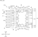
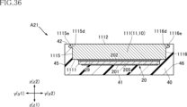
- FIG. 33 to 36 show a first modified example of the semiconductor device A20.
- FIG. 33 is a perspective view of a main part of the semiconductor device A21 according to this modified example.
- FIG. 34 is a plan view of a main part of the semiconductor device A21.
- the outer shape of the sealing resin 40 is shown by an imaginary line (two-dot chain line).
- FIG. 35 is a cross-sectional view showing the semiconductor device A21, and shows a cross-section similar to that of FIG. 31.
- FIG. 36 is a cross-sectional view showing the semiconductor device A21, and shows a cross-section similar to that of FIG. 32.
- the shapes of the fifth protrusion 1113d, the sixth protrusion 1114d, the seventh protrusion 1115d and the seventh protrusion 1115d in the die pad portion 111 are different from those of the semiconductor device A20.
- each of the multiple fifth protrusions 1113d to eighth protrusions 1116d has a portion that is connected to the first back surface 1112.
- the multiple fifth protrusions 1113d to eighth protrusions 1116d are formed, for example, by pressing from the first back surface 1112 side of the die pad portion 111 toward the z1 side in the thickness direction z. In this modified example, pressing is performed on the portions of each protrusion before pressing that are outside the boundary line of the first back surface 1112.
- the die pad portion 111 on which the semiconductor element 20 is mounted has a plurality of fifth protrusions 1113d.
- Each of the plurality of fifth protrusions 1113d protrudes from the first side surface 1113 toward the x1 side in the first direction x.
- the plurality of fifth protrusions 1113d are arranged at intervals in the second direction y. According to the configuration in which the die pad portion 111 has the above-mentioned plurality of fifth protrusions 1113d, the contact area between the die pad portion 111 on which the semiconductor element 20 is mounted and the sealing resin 40 is efficiently increased, and the adhesion between the die pad portion 111 and the sealing resin 40 can be improved.
- the semiconductor device A21 has the same effects as the semiconductor device A20 within the same range of configuration as the semiconductor device A20 of the above embodiment.
- the semiconductor device according to the present disclosure is not limited to the above-mentioned embodiment.
- the specific configuration of each part of the semiconductor device according to the present disclosure can be freely designed in various ways.
- the package structure of the semiconductor device according to the present disclosure is not limited to the structure shown in the semiconductor device A10 of the above embodiment, and the present disclosure can be applied to various package structures.
- Appendix 1 A semiconductor element; a first lead including a die pad portion; a sealing resin covering the semiconductor element and a portion of the first lead, the die pad portion has a first main surface facing one side in a thickness direction and on which a semiconductor element is mounted, a first back surface facing the other side in the thickness direction, a first side surface facing one side in a first direction perpendicular to the thickness direction, and a plurality of first recesses recessed from the first back surface and the first side surface, the first back surface is exposed from the sealing resin,
- the semiconductor device wherein the plurality of first recesses are arranged at intervals in the thickness direction and in a second direction perpendicular to the first direction.
- each of the plurality of first recesses has a first intermediate surface facing the other side in the thickness direction.
- Appendix 3. The semiconductor device according to claim 1, wherein a first dimension, which is a distance between two adjacent first recesses in the second direction, is 1/5 to 5 times a second dimension, which is a length of the first recesses in the second direction.
- Appendix 4. the die pad portion has three or more of the first recessed portions, 4.
- the first recesses are arranged at intervals in the second direction. Appendix 5. 5.
- the die pad portion has a plurality of first protrusions that are connected to the plurality of first recesses and protrude from the first side surface to one side in the first direction.
- the die pad portion has a second side surface facing the other side in the first direction, a third side surface facing one side in the second direction, a fourth side surface facing the other side in the second direction, a plurality of second recesses recessed from the first back surface and the second side surface, a plurality of third recesses recessed from the first back surface and the third side surface, and a plurality of fourth recesses recessed from the first back surface and the fourth side surface,
- the second recesses are arranged at intervals in the second direction
- the third recesses are arranged at intervals in the first direction, 6.
- each of the plurality of second recesses has a second intermediate surface facing the other side in the thickness direction
- Each of the plurality of third recesses has a third intermediate surface facing the other side in the thickness direction
- each of the plurality of fourth recesses has a fourth intermediate surface facing the other side in the thickness direction.
- a third dimension that is a distance between two adjacent second recesses in the second direction is 1/5 to 5 times a fourth dimension that is a length of the second recesses in the second direction;
- a fifth dimension that is a distance between two of the third recesses adjacent to each other in the first direction is 1/5 to 5 times a sixth dimension that is a length of the third recesses in the first direction;
- the die pad portion has three or more of the second recesses, three or more of the third recesses, and three or more of the fourth recesses,
- the second recesses are arranged at intervals in the second direction
- the third recesses are arranged at intervals in the first direction
- the die pad portion has a plurality of second protrusions connected to each of the plurality of second recesses and protruding from the second side surface to the other side in the first direction, a plurality of third protrusions connected to each of the plurality of third recesses and protruding from the third side surface to one side in the second direction, and a plurality of fourth protrusions connected to each of the plurality of fourth recesses and protruding from the fourth side surface to the other side in the second direction.
- Appendix 11 is a plurality of second protrusions connected to each of the plurality of second recesses and protruding from the second side surface to the other side in the first direction
- a plurality of third protrusions connected to each of the plurality of third recesses and protruding from the third side surface to one side in the second direction
- a plurality of fourth protrusions connected to each of the plurality of fourth recesses and protruding from the fourth side surface to the other side
- the die pad portion has a first corner where the first side surface and the third side surface are in contact, a second corner where the first side surface and the fourth side surface are in contact, a third corner where the second side surface and the third side surface are in contact, and a fourth corner where the second side surface and the fourth side surface are in contact,
- Each of the plurality of first recesses is not in contact with either the first corner portion or the second corner portion
- Each of the plurality of second recesses is not in contact with either the third corner portion or the fourth corner portion
- Each of the third recesses is not in contact with either the first corner portion or the third corner portion, 11.
- each of the plurality of fourth recesses is not in contact with either the second corner portion or the fourth corner portion.
- Appendix 12. The semiconductor device according to any one of claims 6 to 11, wherein the semiconductor element does not overlap any of the plurality of first recesses, the plurality of second recesses, the plurality of third recesses, or the plurality of fourth recesses when viewed in the thickness direction.
- Appendix 13. the semiconductor element has a first electrode and a third electrode arranged on one side in the thickness direction, and a second electrode arranged on the other side in the thickness direction, 13.
- the semiconductor element is a switching element having a drain electrode, a source electrode, and a gate electrode; 14.
- the semiconductor device wherein the first electrode is the source electrode, the second electrode is the drain electrode, and the third electrode is the gate electrode.
- Appendix 15. A vehicle comprising a power conversion device configured to include the semiconductor device according to claim 14.
- Appendix 16. A semiconductor element; a first lead including a die pad portion; a sealing resin covering the semiconductor element and a portion of the first lead, the die pad portion has a first main surface facing one side in a thickness direction and on which a semiconductor element is mounted, a first back surface facing the other side in the thickness direction, a first side surface facing one side in a first direction perpendicular to the thickness direction, and a plurality of fifth protrusions protruding from the first side surface to one side in the first direction, the first back surface is exposed from the sealing resin, A semiconductor device, wherein the plurality of fifth protrusions are located toward the other side of the first side in the thickness direction and are arranged at intervals in a second direction perpendicular to the thickness direction and the first direction.
- each of the plurality of fifth protrusions has a fifth intermediate surface facing the other side in the thickness direction.
- Appendix 18. the die pad portion has a second side surface facing the other side in the first direction, a third side surface facing one side in the second direction, a fourth side surface facing the other side in the second direction, a plurality of sixth protruding portions protruding from the second side surface to the other side in the first direction, a plurality of seventh protruding portions protruding from the third side surface to one side in the second direction, and a plurality of eighth protruding portions protruding from the fourth side surface to the other side in the second direction,
- the sixth protrusions are located toward the other side of the second side surface in the thickness direction and are arranged at intervals in the second direction
- the seventh protrusions are located toward the other side of the third side surface in the thickness direction and are arranged at intervals in the first direction, 18.
- each of the sixth protrusions has a sixth intermediate surface facing the other side in the thickness direction
- Each of the seventh protrusions has a seventh intermediate surface facing the other side in the thickness direction
- each of the multiple eighth protrusions has an eighth intermediate surface facing the other side in the thickness direction. Appendix 20.
- the die pad portion has a first corner where the first side surface and the third side surface are in contact, a second corner where the first side surface and the fourth side surface are in contact, a third corner where the second side surface and the third side surface are in contact, and a fourth corner where the second side surface and the fourth side surface are in contact,
- Each of the plurality of fifth protrusions is not in contact with either the first corner portion or the second corner portion
- each of the sixth protrusions is not in contact with either the third corner portion or the fourth corner portion
- each of the seventh protrusions is not in contact with either the first corner portion or the third corner portion
Landscapes
- Structures Or Materials For Encapsulating Or Coating Semiconductor Devices Or Solid State Devices (AREA)
Priority Applications (2)
| Application Number | Priority Date | Filing Date | Title |
|---|---|---|---|
| JP2025523425A JPWO2024247688A1 (https=) | 2023-06-02 | 2024-05-13 | |
| US19/400,369 US20260082923A1 (en) | 2023-06-02 | 2025-11-25 | Semiconductor device and vehicle |
Applications Claiming Priority (2)
| Application Number | Priority Date | Filing Date | Title |
|---|---|---|---|
| JP2023091932 | 2023-06-02 | ||
| JP2023-091932 | 2023-06-02 |
Related Child Applications (1)
| Application Number | Title | Priority Date | Filing Date |
|---|---|---|---|
| US19/400,369 Continuation US20260082923A1 (en) | 2023-06-02 | 2025-11-25 | Semiconductor device and vehicle |
Publications (1)
| Publication Number | Publication Date |
|---|---|
| WO2024247688A1 true WO2024247688A1 (ja) | 2024-12-05 |
Family
ID=93657503
Family Applications (1)
| Application Number | Title | Priority Date | Filing Date |
|---|---|---|---|
| PCT/JP2024/017605 Ceased WO2024247688A1 (ja) | 2023-06-02 | 2024-05-13 | 半導体装置および車両 |
Country Status (3)
| Country | Link |
|---|---|
| US (1) | US20260082923A1 (https=) |
| JP (1) | JPWO2024247688A1 (https=) |
| WO (1) | WO2024247688A1 (https=) |
Citations (6)
| Publication number | Priority date | Publication date | Assignee | Title |
|---|---|---|---|---|
| WO2011049128A1 (ja) * | 2009-10-20 | 2011-04-28 | ローム株式会社 | 半導体装置および半導体装置の製造方法 |
| JP2011517113A (ja) * | 2008-04-08 | 2011-05-26 | フリースケール セミコンダクター インコーポレイテッド | 成形密着性を向上させたパッケージ化電子デバイス用リードフレーム |
| JP2018129442A (ja) * | 2017-02-09 | 2018-08-16 | エイブリック株式会社 | 半導体装置およびその製造方法 |
| JP2020038914A (ja) * | 2018-09-05 | 2020-03-12 | ローム株式会社 | 半導体装置 |
| US20200135625A1 (en) * | 2018-10-30 | 2020-04-30 | Stmicroelectronics, Inc. | Semiconductor package having die pad with cooling fins |
| WO2022014387A1 (ja) * | 2020-07-16 | 2022-01-20 | ローム株式会社 | 半導体装置、および半導体装置の製造方法 |
-
2024
- 2024-05-13 JP JP2025523425A patent/JPWO2024247688A1/ja active Pending
- 2024-05-13 WO PCT/JP2024/017605 patent/WO2024247688A1/ja not_active Ceased
-
2025
- 2025-11-25 US US19/400,369 patent/US20260082923A1/en active Pending
Patent Citations (6)
| Publication number | Priority date | Publication date | Assignee | Title |
|---|---|---|---|---|
| JP2011517113A (ja) * | 2008-04-08 | 2011-05-26 | フリースケール セミコンダクター インコーポレイテッド | 成形密着性を向上させたパッケージ化電子デバイス用リードフレーム |
| WO2011049128A1 (ja) * | 2009-10-20 | 2011-04-28 | ローム株式会社 | 半導体装置および半導体装置の製造方法 |
| JP2018129442A (ja) * | 2017-02-09 | 2018-08-16 | エイブリック株式会社 | 半導体装置およびその製造方法 |
| JP2020038914A (ja) * | 2018-09-05 | 2020-03-12 | ローム株式会社 | 半導体装置 |
| US20200135625A1 (en) * | 2018-10-30 | 2020-04-30 | Stmicroelectronics, Inc. | Semiconductor package having die pad with cooling fins |
| WO2022014387A1 (ja) * | 2020-07-16 | 2022-01-20 | ローム株式会社 | 半導体装置、および半導体装置の製造方法 |
Also Published As
| Publication number | Publication date |
|---|---|
| US20260082923A1 (en) | 2026-03-19 |
| JPWO2024247688A1 (https=) | 2024-12-05 |
Similar Documents
| Publication | Publication Date | Title |
|---|---|---|
| JP7519498B2 (ja) | 半導体装置および車両 | |
| US11631623B2 (en) | Power semiconductor device and method of manufacturing the same, and power conversion device | |
| EP2674973B1 (en) | Power semiconductor module | |
| JP5217884B2 (ja) | 半導体装置 | |
| JP7555257B2 (ja) | 電気回路体、電力変換装置、および電気回路体の製造方法 | |
| CN112864113B (zh) | 功率器件、功率器件组件与相关装置 | |
| US9754855B2 (en) | Semiconductor module having an embedded metal heat dissipation plate | |
| CN100435333C (zh) | 电力半导体装置 | |
| EP2020683A1 (en) | Semiconductor device and method for manufacturing same | |
| CN113113401B (zh) | 半导体电路和半导体电路的制造方法 | |
| EP3796374A1 (en) | Semiconductor device | |
| JP3829641B2 (ja) | パワー半導体モジュール | |
| WO2024247688A1 (ja) | 半導体装置および車両 | |
| JP2024077117A (ja) | 半導体装置、半導体装置の製造方法および電力変換装置 | |
| JP5621812B2 (ja) | 半導体装置 | |
| US20260082945A1 (en) | Semiconductor device and vehicle | |
| US20260060100A1 (en) | Semiconductor device and vehicle | |
| WO2024209899A1 (ja) | 半導体装置および車両 | |
| US20250174527A1 (en) | Semiconductor device | |
| US20260090403A1 (en) | Semiconductor device and vehicle | |
| JP7681920B2 (ja) | 半導体パッケージ及びその製造方法 | |
| JPS5840848A (ja) | 絶縁型半導体装置 | |
| WO2024190426A1 (ja) | 半導体装置および車両 | |
| US20260053054A1 (en) | Semiconductor device, method for manufacturing semiconductor device, and vehicle | |
| WO2024225036A1 (ja) | 半導体装置および車両 |
Legal Events
| Date | Code | Title | Description |
|---|---|---|---|
| 121 | Ep: the epo has been informed by wipo that ep was designated in this application |
Ref document number: 24815172 Country of ref document: EP Kind code of ref document: A1 |
|
| ENP | Entry into the national phase |
Ref document number: 2025523425 Country of ref document: JP Kind code of ref document: A |
|
| NENP | Non-entry into the national phase |
Ref country code: DE |