WO2024242014A1 - 光検出装置および電子機器 - Google Patents
光検出装置および電子機器 Download PDFInfo
- Publication number
- WO2024242014A1 WO2024242014A1 PCT/JP2024/018110 JP2024018110W WO2024242014A1 WO 2024242014 A1 WO2024242014 A1 WO 2024242014A1 JP 2024018110 W JP2024018110 W JP 2024018110W WO 2024242014 A1 WO2024242014 A1 WO 2024242014A1
- Authority
- WO
- WIPO (PCT)
- Prior art keywords
- pixel
- width
- photoelectric conversion
- separation wall
- conversion region
- Prior art date
- Legal status (The legal status is an assumption and is not a legal conclusion. Google has not performed a legal analysis and makes no representation as to the accuracy of the status listed.)
- Ceased
Links
Images











Classifications
-
- H—ELECTRICITY
- H04—ELECTRIC COMMUNICATION TECHNIQUE
- H04N—PICTORIAL COMMUNICATION, e.g. TELEVISION
- H04N25/00—Circuitry of solid-state image sensors [SSIS]; Control thereof
- H04N25/70—SSIS architectures; Circuits associated therewith
-
- H—ELECTRICITY
- H10—SEMICONDUCTOR DEVICES; ELECTRIC SOLID-STATE DEVICES NOT OTHERWISE PROVIDED FOR
- H10F—INORGANIC SEMICONDUCTOR DEVICES SENSITIVE TO INFRARED RADIATION, LIGHT, ELECTROMAGNETIC RADIATION OF SHORTER WAVELENGTH OR CORPUSCULAR RADIATION
- H10F39/00—Integrated devices, or assemblies of multiple devices, comprising at least one element covered by group H10F30/00, e.g. radiation detectors comprising photodiode arrays
- H10F39/10—Integrated devices
- H10F39/12—Image sensors
Definitions
- the photodetection device includes: A photoelectric conversion region formed on a semiconductor substrate; a pixel separating section that penetrates the semiconductor substrate and separates the photoelectric conversion region into individual pixels; the pixel separation section has a first separation wall on a first surface side of the semiconductor substrate and a second separation wall on a second surface side of the semiconductor substrate opposite to the first surface,
- the first and second separation walls have different widths, With respect to a width of the photoelectric conversion region to the second separation wall in a direction perpendicular to a center line that divides the photoelectric conversion region in two horizontally or vertically, a first width at a center part of a side of a pixel is larger than a second width at a portion near a corner of the pixel.
- An electronic device includes: A photoelectric conversion region formed on a semiconductor substrate; a pixel separating section that penetrates the semiconductor substrate and separates the photoelectric conversion region into individual pixels; the pixel separation section has a first separation wall on a first surface side of the semiconductor substrate and a second separation wall on a second surface side of the semiconductor substrate opposite to the first surface, The first and second separation walls have different widths,
- the photodetector device is configured such that, with respect to the width of the photoelectric conversion region to the second separation wall in a direction perpendicular to a center line that horizontally or vertically divides the photoelectric conversion region, a first width at the center of a side of a pixel is larger than a second width at a portion near a corner of the pixel.
- the light detection device and electronics may be standalone devices or may be modules that are incorporated into other devices.
- FIG. 1 is a diagram illustrating a schematic configuration of a solid-state imaging device according to an embodiment of the present disclosure.
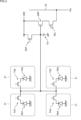
- FIG. 2 is a diagram illustrating an example of a circuit configuration of a pixel.
- FIG. 2 is a cross-sectional view showing a first structure example of a pixel.
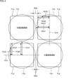
- FIG. 2 is a plan view of a pixel separator in the first structure example of the pixel.
- FIG. 13 is a plan view of a pixel separator in a modified example of the first structure example of the pixel.
- 11A to 11C are diagrams illustrating an effect of a pixel separating portion in the first structure example of the pixel.
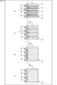
- 5A to 5C are diagrams illustrating a method for forming a pixel separating portion of the pixel according to the first structural example.
- FIG. 5A to 5C are diagrams illustrating a method for forming a pixel separating portion of the pixel according to the first structural example.
- 5A to 5C are diagrams illustrating a method for forming a pixel separating portion of the pixel according to the first structural example.
- FIG. 11 is a cross-sectional view showing a second structure example of a pixel.
- FIG. 13 is a plan view of a pixel separator in a second structure example of the pixel.
- 13A to 13C are diagrams illustrating the effect of a pixel separating portion in the second example of the pixel structure.
- FIG. 13 is a plan view showing a modified example of a pixel.
- FIG. 13 is a plan view showing a modified example of a pixel.
- FIG. 13 is a plan view showing a modified example of a pixel.
- Example of a schematic configuration of a solid-state imaging device 2.
- Example of a circuit configuration of a pixel 3.
- First example of a pixel structure 4.
- Method of forming a pixel separation section of the first example of a structure 5.
- Second example of a pixel structure 6.
- Modified example of a pixel 7.
- Staggered arrangement of rectangular pixels 8.
- Example of use of an image sensor 9.
- Example of application to electronic devices 10.
- the technology disclosed herein can be applied to photodetection devices in general that have a pixel array in which pixels are arranged two-dimensionally in a matrix, and that perform photoelectric conversion of incident light to output a pixel signal according to the amount of light.
- the technology disclosed herein can be applied to a solid-state imaging device that generates and outputs an imaging signal according to the amount of incident light, or a light receiving device (distance measuring sensor) of a distance measuring system that receives infrared light irradiated as active light and measures the distance to a subject using a direct ToF method or an indirect ToF method.
- a light receiving device distance measuring sensor
- a distance measuring system that receives infrared light irradiated as active light and measures the distance to a subject using a direct ToF method or an indirect ToF method.
- FIG. 1 is a diagram showing a schematic configuration of a solid-state imaging device according to an embodiment of the present disclosure.
- the solid-state imaging device 1 in FIG. 1 includes a pixel array section 11 and a peripheral circuit section.
- the peripheral circuit section includes, for example, a vertical drive section 12, a column processing section 13, a horizontal drive section 14, and a system control section 15.
- the solid-state imaging device 1 further includes a signal processing unit 16 and a data storage unit 17.
- the signal processing unit 16 and the data storage unit 17 may be mounted on the same substrate as the pixel array unit 11, the vertical drive unit 12, etc., or may be disposed on a separate substrate.
- the signal processing unit 16 and the data storage unit 17 may also be provided on a semiconductor chip separate from the solid-state imaging device 1.
- the pixel array section 11 has a configuration in which a plurality of pixels 21 are arranged two-dimensionally in a matrix in the row and column directions.
- the row direction refers to the pixel rows of the pixel array section 11, i.e., the horizontal arrangement direction
- the column direction refers to the pixel columns of the pixel array section 11, i.e., the vertical arrangement direction.
- the pixel 21 has a photoelectric conversion unit that generates and accumulates an electric charge according to the amount of light received, and a plurality of pixel transistors (so-called MOS transistors). A specific example of the circuit configuration of the pixel 21 will be described later with reference to FIG. 2 etc.
- pixel drive lines 22 are wired in the row direction as row signal lines for each pixel row, and vertical signal lines 23 are wired in the column direction as column signal lines for each pixel column.
- the pixel drive lines 22 transmit drive signals for driving the pixels 21 when reading out signals.
- the pixel drive line 22 is shown as a single wire, but is not limited to one.
- One end of the pixel drive line 22 is connected to an output terminal corresponding to each row of the vertical drive section 12.
- the readout scanning system sequentially selects and scans the pixels 21 of the pixel array section 11 row by row in order to read out signals from the pixels 21.
- the signals read out from the pixels 21 are analog signals.
- the sweep scanning system performs sweep scanning on the readout row on which the readout scanning system performs readout scanning, prior to the readout scanning by the exposure time.
- the sweep-out scan by this sweep-out scanning system sweeps out unnecessary charges from the photoelectric conversion units of the pixels 21 in the readout row, thereby resetting the photoelectric conversion units of each pixel 21. Then, by sweeping out (resetting) the unnecessary charges by this sweep-out scanning system, a so-called electronic shutter operation is performed.
- the electronic shutter operation refers to the operation of discarding the charge in the photoelectric conversion unit and starting a new exposure (starting the accumulation of charge).
- the signal read out by the read operation by the read scanning system corresponds to the amount of light received since the immediately preceding read operation or electronic shutter operation.
- the period from the read timing of the immediately preceding read operation or the sweep timing of the electronic shutter operation to the read timing of the current read operation is the exposure period of pixel 21.
- the signals output from each pixel 21 in the pixel row selected and scanned by the vertical drive unit 12 are input to the column processing unit 13 through each vertical signal line 23 for each pixel column.
- the column processing unit 13 performs a predetermined signal processing on the signals output from each pixel 21 in the selected row through the vertical signal line 23 for each pixel column in the pixel array unit 11, and temporarily holds the pixel signals after signal processing.
- the system control unit 15 is composed of a timing generator that generates various timing signals, and controls the driving of the vertical driving unit 12, column processing unit 13, and horizontal driving unit 14 based on the various timings generated by the timing generator.
- the signal processing unit 16 has at least an arithmetic processing function, and performs various signal processing such as arithmetic processing on the pixel signals output from the column processing unit 13.
- the data storage unit 17 temporarily stores data necessary for the signal processing in the signal processing unit 16.
- the pixel signals that have been signal processed in the signal processing unit 16 are converted into a predetermined format and output from the output unit 18 to the outside of the device.
- FIG. 2 shows an example of the circuit configuration of each pixel 21 arranged two-dimensionally in a matrix in the pixel array section 11.
- each pixel 21 has a shared pixel structure in which a readout circuit that reads out the signal of each pixel is shared by four pixels (2x2) in the row and column directions.
- the photodiode PD as a photoelectric conversion section and the transfer transistor TG are provided for each pixel, and the floating diffusion region FD, reset transistor RST, amplification transistor AMP, and selection transistor SEL are shared by four pixels, which are a shared unit.
- Each pixel transistor of the transfer transistor TG, reset transistor RST, amplification transistor AMP, and selection transistor SEL is made up of an N-type MOS transistor (MOS FET), and constitutes a readout circuit.
- MOS FET N-type MOS transistor
- numbers 1 through 4 are added to distinguish the photodiodes PD and transfer transistors TG of the four pixels that share the readout circuit, such as photodiodes PD1 through PD4 and transfer transistors TG1 through TG4.
- the photodiode PD generates and accumulates an electric charge (signal charge) according to the amount of light received.
- the anode terminal of the photodiode PD is grounded, and the cathode terminal is connected to the floating diffusion region FD via the transfer transistor TG.
- the transfer transistor TG When the transfer transistor TG is turned on by a transfer drive signal supplied to its gate electrode, it reads out the charge generated in the photodiode PD and transfers it to the floating diffusion region FD.
- the floating diffusion region FD holds the charge read out from at least one of the four photodiodes PD.
- the reset transistor RST When the reset transistor RST is turned on by a reset drive signal supplied to the gate electrode, the charge stored in the floating diffusion region FD is discharged to the drain (power supply voltage VDD), resetting the potential of the floating diffusion region FD.
- the amplification transistor AMP outputs a signal according to the potential of the floating diffusion region FD. That is, the amplification transistor AMP forms a source follower circuit with a load MOS transistor (not shown) as a constant current source connected via a vertical signal line 23, and a signal VSL indicating a level according to the charge accumulated in the floating diffusion region FD is output from the amplification transistor AMP to the column processing unit 13 ( Figure 1) via the selection transistor SEL.
- the selection transistor SEL is turned on when a shared unit is selected by a selection drive signal supplied to the gate electrode, and outputs a signal VSL generated in each pixel 21 of the shared unit to the column processing unit 13 via a vertical signal line 23.
- the transfer drive signal, selection drive signal, and reset drive signal are supplied from the vertical drive unit 12 via the pixel drive line 22 in FIG. 1.
- the four pixels 21 in the shared unit (2x2) share and use the reset transistor RST, the amplification transistor AMP, and the selection transistor SEL.
- the solid-state imaging device 1 can, for example, select and perform the following driving modes as appropriate depending on the operating mode.
- the solid-state imaging device 1 can turn on the transfer transistors TG of the four pixels in a shared unit in sequence, one pixel at a time, transfer the charge generated in the photodiode PD of one pixel to the floating diffusion region FD, and output the signal VSL to the column processing unit 13 via the vertical signal line 23.
- the solid-state imaging device 1 can turn on the transfer transistors TG of two adjacent pixels in the row or column direction among the four pixels in a shared unit, and simultaneously transfer the charges generated in the photodiodes PD of the two pixels to the floating diffusion region FD, which is then output as a signal VSL to the column processing unit 13 via the vertical signal line 23.
- the solid-state imaging device 1 can simultaneously turn on the transfer transistors TG of all four pixels in a shared unit, simultaneously transfer the charges generated in the photodiodes PD of the four pixels to the floating diffusion regions FD, and output the signals VSL to the column processing unit 13 via the vertical signal line 23.
- each pixel 21 shares a readout circuit is not limited to four pixels.
- a circuit configuration in which a readout circuit is shared by eight pixels (4x2 or 2x4) may be adopted.
- each pixel 21 may also have a configuration in which the readout circuit is not shared but is provided individually for each pixel.
- FIG. 3 is a cross-sectional view showing a first structural example of the pixel 21. As shown in FIG. 3
- the pixel 21 described below is an example of a back-illuminated type, but this technology can also be applied to a front-illuminated type.
- the pixel 21 shown in FIG. 3 is formed on a semiconductor substrate 51 using, for example, silicon (Si) as a semiconductor material.
- a first surface 51a on the upper side of the semiconductor substrate 51 is the front surface of the semiconductor substrate 51, and pixel transistors such as a transfer transistor TG, an amplifying transistor AMP, and a reset transistor RST, as well as a multi-layer wiring layer are formed on the first surface 51a, but are not shown.
- the multi-layer wiring layer is a layer that includes one or more layers of wiring made of a metal material such as copper (Cu), tungsten (W), or aluminum (Al), and an interlayer insulating film made of a silicon oxide film or the like.
- a second surface 51b on the lower side of the semiconductor substrate 51 is the back surface of the semiconductor substrate 51, and is a light incident surface into which light is incident.
- a P-type semiconductor region 61 formed on the first surface 51a side and an N-type semiconductor region 62 formed on the second surface 51b side are formed for each pixel, and a photodiode PD is formed using a PN junction between the P-type semiconductor region 61 and the N-type semiconductor region 62.
- the P-type semiconductor region 61 and the N-type semiconductor region 62 are part of the photoelectric conversion region of the pixel 21.
- a pixel separation section 71 is formed to separate the photoelectric conversion region formed for each pixel into pixel units.
- the pixel separation section 71 is composed of a first separation wall 71a and a second separation wall 71b of different widths, and penetrates the semiconductor substrate 51 to completely separate the photoelectric conversion region formed for each pixel.
- the width of the first separation wall 71a on the front surface side of the semiconductor substrate 51 is formed larger than the width of the second separation wall 71b on the back surface side (width of the first separation wall 71a > width of the second separation wall 71b).
- the first separation wall 71a is formed by embedding a sidewall 72 and an insulating film 73
- the second separation wall 71b is formed by embedding only the insulating film 73.
- the sidewall 72 is formed of an oxide film (SiO2), a nitride film (SiN), or a laminate thereof.
- the insulating film 73 is formed of, for example, SiO2, SiN, undoped polysilicon, Al2O3, or the like.
- a P-type semiconductor region 74 and an N-type semiconductor region 75 are formed in that order toward the center (inside) of the pixel 21.
- the P-type semiconductor region 74 and the N-type semiconductor region 75 are also part of the photoelectric conversion region of the pixel 21.
- the N-type semiconductor region 62 and the N-type semiconductor region 75 have different impurity concentrations, and the N-type semiconductor region 75 is a region with a higher concentration than the N-type semiconductor region 62.
- the P-type semiconductor region 74 is formed with a high concentration along the side wall of the second separation wall 71b, thereby suppressing electrons from the interface of the second separation wall 71b.
- the saturation charge amount Qs can be increased.
- the P-type semiconductor region 74 and the N-type semiconductor region 75 are formed, for example, by conformal doping.
- Conformal doping is an impurity region formation method including, for example, a solid-phase diffusion method and a plasma doping method.
- a planarization film 81 is formed on the second surface 51b, which is the light incidence surface of the semiconductor substrate 51.
- a light-shielding film 82 is formed at the pixel boundary inside the planarization film 81.
- the light-shielding film 82 is provided to prevent light from leaking into adjacent pixels 21.
- the light-shielding film 82 is made of a metal material such as W (tungsten).
- an OCL (on-chip lens) 83 is formed to focus the incident light onto the photodiode PD.
- the OCL 83 can be made of an inorganic material, such as SiN, SiO, or SiOxNy (where 0 ⁇ x ⁇ 1, 0 ⁇ y ⁇ 1).
- a transparent plate such as cover glass or resin may be bonded to the OCL 83.
- a color filter layer may be formed between the OCL 83 and the planarization film 81.
- the color filter arrangement may be, for example, a Bayer arrangement in which R (red), G (green), G (green), and B (blue) color filters are arranged in 2 ⁇ 2 four pixels, or a quad Bayer arrangement in which R, G, G, and B color filters are arranged in a Bayer arrangement in 2 ⁇ 2 four-pixel units with the arrangement unit of one color being 2 ⁇ 2 four pixels.
- the pixel 21 has a pixel separation section 71 consisting of a first separation wall 71a and a second separation wall 71b formed with different widths depending on the depth position of the semiconductor substrate 51.
- the first separation wall 71a and the second separation wall 71b are configured with different planar shapes.
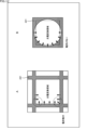
- Figure 4 is a plan view that shows a schematic diagram of the planar shapes of the first separation wall 71a and the second separation wall 71b.
- the first separation wall 71a' is formed linearly except for the corners of the photoelectric conversion region, and has a substantially rectangular planar shape.
- the second separation wall 71b' has a substantially circular planar shape.
- the width DSa between the first separation walls 71a' of adjacent pixels 21 is larger (wider) than the width DSb between the second separation walls 71b'.
- the manufacturing method of the pixel separation section 71 will be described later, but such differences in planar shape arise during the manufacturing process due to the presence or absence of sidewalls 72 and migration of the semiconductor layer (Si) when a hydrogen bake process (H2 bake) is performed.
- the first width HLb1 to the second separation wall 71b' at the center of the side is larger than the second width HLb2 to the second separation wall 71b' near the corner (first width HLb1 > second width HLb2).
- the first width HLb1 to the second separation wall 71b' at the center of the side is larger than the first width HUa1 to the first separation wall 71a' (first width HLb1 > first width HUa1).
- the width HLb of the photoelectric conversion region in the direction perpendicular to the center line 101h gradually decreases from the center of the side of the photoelectric conversion region toward the vicinity of the corner (first width HLb1 ⁇ second width HLb2).
- the second width HLb2 to the second separation wall 71b' is smaller than the second width HUa2 to the first separation wall 71a' (second width HLb2 ⁇ second width HUa2).
- the first width VLb1 to the second separation wall 71b' at the center of the side is larger than the second width VLb2 to the second separation wall 71b' near the corner (first width VLb1 > second width VLb2).
- the second width VUa2 to the first separation wall 71a' is larger than the second width VLb2 to the second separation wall 71b' (second width VUa2 > second width VLb2).
- FIG. 5 is a plan view showing a modified example of the first structural example of pixel 21, and similar to FIG. 4, shows a schematic planar shape of first separation wall 71a and second separation wall 71b.
- the width HLb of the photoelectric conversion region in the direction perpendicular to the center line 101h is the same as or smaller than the center of the side as it moves from the center of the side of the photoelectric conversion region toward the vicinity of the corner (first width HLb1 ⁇ second width HLb2).
- the width VLb of the photoelectric conversion region in the direction perpendicular to the center line 101v is the same as or smaller than the center of the side as it moves from the center of the side of the photoelectric conversion region toward the vicinity of the corner (first width VLb1 ⁇ second width VLb2).
- the pixel 21 according to the first structural example is characterized in that the planar shape of the pixel separation section 71, which completely separates the photoelectric conversion regions of each pixel, has a substantially rectangular planar shape at the first separation wall 71a close to the first surface 51a, which is the front surface of the semiconductor substrate 51, and has a substantially circular or octagonal planar shape at the second separation wall 71b, which is deeper than that.
- a in FIG. 6 shows a plan view and a potential diagram of a photoelectric conversion region when the photoelectric conversion region separated by the second separation wall 71b of the pixel separation section 71 is formed in a rectangular shape.
- FIG. 6 shows a plan view and a potential diagram of a photoelectric conversion region when the photoelectric conversion region separated by the second separation wall 71b of the pixel separation section 71 is formed in a circular shape.
- the P-type semiconductor region 74 and the N-type semiconductor region 75 are formed by conformal doping along the second separation wall 71b.
- doping is performed twice at the corner of the photoelectric conversion region in FIG. 6A, from the horizontal direction of the second separation wall 71b and from the vertical direction. Therefore, when comparing potential 121Xp directed from the corner toward the pixel center, indicated by arrow 121X, with potential 121Yp directed from the center of the side toward the pixel center, indicated by arrow 121Y, a region with a deep potential is formed at the corner. As a result of the difference between potential 121Xp and potential 121Yp, it becomes difficult to design the charge transfer.
- the planar shape of the pixel separation section 71 is such that the first separation wall 71a close to the front surface side of the semiconductor substrate 51 has a substantially rectangular planar shape, and the second separation wall 71b deeper than that has a substantially circular or substantially octagonal planar shape, thereby improving charge transfer within the photoelectric conversion region.
- the front surface side of the semiconductor substrate 51 is preferably linear in order to form the transfer transistor TG and the floating diffusion region FD
- the planar shape of the first separation wall 71a is preferably substantially rectangular.
- Fig. 7 and Fig. 8 show cross-sectional views of the formation of three pixel separating portions 71 arranged in the horizontal or vertical direction of the pixel array portion 11.
- a hard mask 201 made of SiN, SiO2, or the like is formed in a predetermined region of the first surface 51a, which is the front surface of the semiconductor substrate 51.
- the region in which the hard mask 201 is formed is a region other than the region in which the first separation wall 71a of the pixel separation section 71 is formed.
- a portion of the semiconductor substrate 51 is removed by dry etching based on the hard mask 201, and a trench 202 with a depth corresponding to the first separation wall 71a is formed.
- the planar shape of the trench 202 is a lattice shape that follows the pixel boundary portion.
- sidewalls 72 are formed on the sidewalls of trench 202.
- Sidewalls 72 can be formed, for example, by stacking oxide films, nitride films, etc. by CVD, ALD, etc., and then etching them back by the RIE method.
- dry etching is performed using the hard mask 201 and the sidewall 72 as a mask to form a trench 203 with a depth corresponding to the second isolation wall 71b.
- the planar shape of the trench 203 is as shown in FIG. 9A.
- N-type semiconductor regions 75 are formed on the sidewalls of trenches 203 by conformal doping using an N-type impurity such as P (phosphorus).
- an N-type impurity such as P (phosphorus).
- P phosphorus
- a solid-phase diffusion method or a plasma doping method can be used for conformal doping.
- hydrogen bake processing (H2 bake) is performed in situ.
- the hydrogen bake processing causes migration of the silicon layer of the semiconductor substrate 51 near the sidewall of the trench 203 that is not covered by the sidewall 72, and the planar shape of the trench 203 that becomes the second isolation wall 71b deep from the front surface side of the semiconductor substrate 51 becomes an approximately circular or approximately octagonal planar shape, as shown by the dashed line in B of FIG. 9. If the hydrogen bake processing is insufficient, streak defects will occur due to the remaining natural oxide film at the interface between the silicon layer of the semiconductor substrate 51 and the silicon layer 221 formed by epitaxial growth in the next process, and the dark characteristics will deteriorate.
- a silicon layer 221 is formed on the sidewall of the trench 203 by epitaxial growth.
- a P-type impurity such as B (boron)
- a P-type semiconductor region 74 is formed on the sidewall of the trench 203 as shown in FIG. 8C.
- an insulating film 73 such as SiO2 or SiN is embedded inside the trench 203 to complete the first separation wall 71a and the second separation wall 71b that constitute the pixel separation section 71.
- the second surface 51b which is the back surface side of the semiconductor substrate 51, is thinned to a thickness that exposes the second separation wall 71b.
- the pixel separation section 71 of the first structural example can be formed as described above.
- FIG. 10 is a cross-sectional view showing a second structure example of the pixel 21. As shown in FIG. 10
- the second structural example in FIG. 10 differs from the first structural example in that a conductive material 241, rather than an insulating film 73, is embedded in the middle of the first and second separation walls 71a and 71b that constitute the pixel separation section 71, and a predetermined bias voltage (e.g., negative bias) is applied to it, but is otherwise common to both structural examples.
- the conductive material 241 is composed of, for example, polysilicon, doped polysilicon doped with N-type or P-type impurities, a transparent electrode such as ITO (indium tin oxide) or ZnO, or the like.
- FIG. 11 is a schematic plan view showing the planar shape of the conductive material 241 that is part of the pixel separator 71.
- the conductive material 241 of the first separation wall 71a along line XX' in Figure 10 has a substantially rectangular planar shape as shown by the solid line, and the conductive material 241 of the second separation wall 71b along line YY' in Figure 10 has a substantially circular planar shape as shown by the dashed line.
- the planar shape of the conductive material 241 of the pixel separation section 71 is formed in a rectangular shape as shown in A of FIG. 12, the electric field from the conductive material 241 to which a negative bias is applied is generated from both the horizontal sides (side walls) and the vertical sides (side walls), so that the electric field concentrates at the corners of the photoelectric conversion region, resulting in a weak spot in reliability, such as a deterioration in the TDDB (Time Dependent Dielectric Breakdown) life.
- the planar shape of the conductive material 241 is formed in a circular shape as shown in B of FIG. 12, the electric field from the conductive material 241 becomes uniform, and the planar shape becomes closer to a circular shape, thereby mitigating the electric field concentration and improving the voltage resistance. Therefore, by making the planar shape of the conductive material 241 as part of the pixel separation section 71 approximately circular or approximately octagonal, the reliability of the solid-state imaging device 1 can be improved.
- the pixel 21 according to the second structural example can improve reliability in addition to improving the charge transfer within the photoelectric conversion region in the first structural example.
- FIG. 13 is a plan view showing a modified example of the pixel 21. As shown in FIG. 13
- the first and second structural examples of the pixel 21 described above are pixel structures in which the planar shape of the photodiode PD, which is the photoelectric conversion region, is square, as shown in A of FIG. 13.
- the structure of the pixel separator 71 described above can also be applied to pixel structures in which the photodiode PD, which is the photoelectric conversion region, has a rectangular planar shape, as shown in Figures 13B and 13C.
- B and C of Fig. 13 show a structure in which the photodiode PD has a rectangular planar shape and an overflow path 301 is formed between two photodiodes PD arranged side by side.
- B of Fig. 13 corresponds to the pixel separation section 71 of the first structural example in which the periphery of the photodiode PD is constituted by an insulating film 73
- C of Fig. 13 corresponds to the pixel separation section 71 of the second structural example in which a conductive material 241 is formed around the photodiode PD.
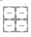
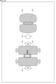
- the photodiode PD has a rectangular planar shape, and an overflow path 301 is formed between two photodiodes PD arranged side by side, as shown in FIG. 14, in which each pixel 21 has a rectangular planar shape, and two pixel regions adjacent in the row direction form a square shape.
- One on-chip lens 311 is disposed for two square-shaped pixels.
- Each pixel 21 shares a floating diffusion region FD with four pixels (2x2), and the floating diffusion region FD is disposed in the center of the four pixel regions that form the shared unit.
- the transfer transistors TG (TG1, TG2, TG3, TG4) of each pixel 21 are disposed near the floating diffusion region FD.
- the vertical drive unit 12 of the solid-state imaging device 1 outputs signals of two pixels sharing one on-chip lens 311 on a pixel-by-pixel basis, there is a phase difference between the R pixel signal received by the pixel 21 (R pixel) on the right side of the on-chip lens 311 and the L pixel signal received by the pixel 21 (L pixel) on the left side, and therefore the signal can be used as a phase difference signal.
- the transfer transistors TG of the two pixels sharing one on-chip lens 311 are turned on simultaneously.
- An overflow path 301 is formed between the photodiodes PD of two pixels that share one on-chip lens 311.
- the overflow path 301 separates the left pixel 21 from the right pixel 21 with a predetermined potential barrier (separation potential).
- the signal charges of the left pixel 21 and the right pixel 21 are stored independently in the respective photodiodes PD until the amount of signal charge reaches the height of the potential barrier of the overflow path 301.
- the signal charge flows from one of the photodiodes PD of the two pixels to the other through the overflow path 301.
- the position of the overflow path 301 formed between the photodiodes PD of the two pixels may be configured to be provided at the end (upper or lower end) of the long side as shown in A and B of FIG. 15, instead of the center of the long side as shown in FIG. 13.
- FIG. 15 shows an example in which the overflow paths 301 are positioned symmetrically in two vertically adjacent pixels, but they may be positioned in the same position at the top or bottom end of the long side of each pixel.
- a pixel 21 in which the planar shape of one pixel is configured as a rectangle and two pixel regions having an overflow path 301 form a square shape is hereinafter referred to as a rectangular pixel 21.
- two rectangular pixels 21 sharing one on-chip lens 311 are referred to as a square unit pixel.
- the rectangular photoelectric conversion region changes as shown in FIG. 16. That is, migration causes the photoelectric conversion region to expand so as to narrow the groove between the two photodiodes PD, and the area of the overflow path 301 also expands. Of the rectangular photoelectric conversion region, the outward expansion of the side in the long side direction increases, and the outward expansion of the side in the short side direction decreases. Note that migration refers to the change in the semiconductor layer (Si) due to the heat of the hydrogen bake process, such that the surface area of the side wall decreases while the volume of the photoelectric conversion region of the photodiode PD remains the same.
- the photoelectric conversion region of the rectangular pixel 21 expands in the left-right direction due to migration, the photoelectric conversion region of the square unit pixel consisting of two rectangular pixels 21 becomes closer to a circle, so that the shape becomes closer to the lens shape of the on-chip lens 311 shown in FIG. 14, making it easier to collect incident light.
- the distance from the overflow path 301 to the center of the photoelectric conversion region of the rectangular pixel 21 increases, so that the effect of P-type ion diffusion in the P-type ion implantation for forming the separation potential of the overflow path 301 can be reduced. This makes it easier to design the transfer of the photodiode PD.
- the corners close to the overflow path 301 of the photoelectric conversion region of the rectangular pixel 21 move in the direction that expands the groove portion due to migration, making it easier to separate pixels other than the overflow path 301 of the two photodiodes PD.
- the line width of the pixel separation sections 71 is formed larger (wider) in advance in anticipation of the decrease in the line width of the pixel separation sections 71 adjacent in the left-right direction, the volume of the photoelectric conversion region per pixel decreases, and the saturation charge amount Qs decreases. Conversely, at the intersections of the pixel separation sections 71 such as region 322, the line width of the pixel separation sections 71 increases, making it difficult to fill the pixel separation sections 71 with the insulating film 73 and conductive material 241.
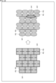
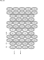
- the square unit pixels are arranged in a staggered arrangement in which the pixel positions are shifted in the column direction by half the pitch of the pixel size from other pixel columns of adjacent square unit pixels, as shown in FIG. 18.
- the long side portion where the photoelectric conversion region of the photodiode PD of the rectangular pixel 21 of one of the adjacent first pixel columns and second pixel columns is bulged is arranged close to the corner portion where the photoelectric conversion region of the photodiode PD of the rectangular pixel 21 of the other adjacent second pixel column, and the photodiode PD of the rectangular pixel 21 can be efficiently arranged in the entire pixel array section 11.
- the staggered arrangement of the rectangular pixels 21 in FIG. 18 can increase the saturation charge amount Qs due to the increased volume of the photoelectric conversion region of the photodiode PD for the same pixel size.
- the staggered arrangement in FIG. 18 allows for a smaller pixel pitch, making it possible to miniaturize the pixels.
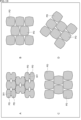
- Figure 19 shows another example of a staggered pixel arrangement.
- a in Figure 19 is another example of a staggered arrangement of square unit pixels.
- the long sides of the rectangular pixels 21 are parallel to the row direction, and the two rectangular pixels 21 that make up a square unit pixel are arranged so that they are aligned in the top-to-bottom direction (column direction) rather than the left-to-right direction (row direction).
- the square unit pixels are arranged such that the pixel positions of the adjacent pixel rows above and below are shifted in the row direction by half the pixel size pitch.
- FIG. 19 shows an example in which pixels 21 of the square pixel structure shown in A of FIG. 13 are arranged in a staggered arrangement in which the pixel positions of pixels 21 in adjacent pixel columns are shifted in the column direction by half the pitch of the pixel size.
- C in FIG. 19 shows an example in which pixels 21 of the square pixel structure shown in A in FIG. 13 are arranged in a staggered arrangement in which the pixel positions of pixels 21 in adjacent pixel rows are shifted in the row direction by half the pitch of the pixel size.
- D in Fig. 19 shows an example in which the pixels 21 of the square pixel structure shown in A in Fig. 13 are rotated 45 degrees in the row and column directions and arranged in a 45-degree inclined direction, a so-called clear bit arrangement, in which the pixel positions are shifted in a 45-degree inclined direction by half the pixel size from the pixels 21 of other adjacent pixel columns.
- FIGS. 20 and 21 are diagrams illustrating examples of color filter arrangements when color filters are arranged for rectangular pixels 21.
- FIG. 20 shows an example of a color filter arrangement in which rectangular pixels 21 are arranged in the staggered arrangement shown in FIG. 18.
- the color filters 341R, 341G, and 341B can be arranged in the same manner as the color filter arrangement in the honeycomb arrangement, as shown in FIG. 20, for example.
- one of the even-numbered or odd-numbered columns of the square unit pixels is a column in which only the green (G) color filter 341G is arranged, and the other is a column in which the green (G) color filter 341G and the red (R) color filter 341R are arranged alternately, or a column in which the blue (B) color filter 341B and the green (G) color filter 341G are arranged alternately.
- the blue color filter 341B and the red color filter 341R are surrounded by square unit pixels of the green color filter 341G.
- the column in which the blue color filter 341B is arranged and the column in which the red color filter 341R is arranged are arranged on either side of the column in which only the green color filter 341G is arranged.
- Figure 21 shows an example of a quad Bayer color filter array.
- the quad Bayer array in FIG. 21 is a color filter array in which the arrangement unit of one color is a 2 ⁇ 2 square unit pixel, and green color filters 341G, red color filters 341R, and blue color filters 341B are arranged in a Bayer array.
- the color filter array of a rectangular pixel 21 is a quad Bayer array, for example, as shown in FIG. 21, square unit pixels having color filters 341 of the same color are arranged so that the orientations of the rectangular pixel 21 in which the blue color filter 341B is arranged and the rectangular pixel 21 in which the red color filter 341R is arranged are perpendicular to the orientation of the rectangular pixel 21 in which the green color filter 341G is arranged.
- Figures 20 and 21 are diagrams for explaining the arrangement of color filters 341R, 341G, and 341B.
- color filters 341R, 341G, and 341B are shown only inside photodiode PD, but in reality, color filters 341R, 341G, and 341B are formed to cover the entire pixel area.
- the color filter array may be an array of complementary color filters of yellow, magenta, and cyan, instead of the three primary colors of R, G, and B described above.
- the method of forming the rectangular pixels 21 in a staggered arrangement is the same as the method of forming the pixel separation portion 71 of the pixel 21 according to the first structure example described with reference to FIGS. 7 to 9.
- the pattern of the hard mask 201 in A of FIG. 7 becomes a pattern that matches the staggered arrangement of the rectangular pixels 21.
- the hydrogen bake process shown in A of FIG. 8 the silicon layer of the semiconductor substrate 51 migrates, and the planar shape of the trench 203 that becomes the second separation wall 71b in the deep part from the front surface side of the semiconductor substrate 51 becomes the shape shown on the right side of FIG. 16.
- a silicon layer 221 is formed on the side wall of the trench 203 by epitaxial growth, and a P-type semiconductor region 74 is formed on the side wall of the trench 203 by conformal doping using a P-type impurity.
- This configuration is an example in which the signal charge is an electron, but in the case where the signal charge is a hole, conformal doping using an N-type impurity is performed on the silicon layer 221 formed by epitaxial growth. If the P-type semiconductor region 74 is not formed, the epitaxial growth step and the conformal doping step are omitted.
- FIG. 22 is a diagram showing an example of use of an image sensor using the above-described solid-state imaging device 1.
- FIG. 22 is a diagram showing an example of use of an image sensor using the above-described solid-state imaging device 1.
- the above-mentioned solid-state imaging device 1 can be used as an image sensor in various cases, for example, to sense light such as visible light, infrared light, ultraviolet light, and X-rays, as follows:
- - Devices that take images for viewing such as digital cameras and mobile devices with camera functions
- - Devices for traffic purposes such as in-vehicle sensors that take images of the front and rear of a car, the surroundings, and the interior of the car for safe driving such as automatic stopping and for recognizing the driver's state, surveillance cameras that monitor moving vehicles and roads, and distance measuring sensors that measure the distance between vehicles, etc.
- - Devices for home appliances such as TVs, refrigerators, and air conditioners that take images of users' gestures and operate devices in accordance with those gestures
- - Devices for medical and healthcare purposes such as endoscopes and devices that take images of blood vessels by receiving infrared light
- - Devices for security purposes such as surveillance cameras for crime prevention and cameras for person authentication
- - Devices for beauty purposes such as skin measuring devices that take images of the skin and microscopes that take images of the scalp
- - Devices for sports such as action cameras and wearable cameras for sports purposes, etc.
- - Devices for agricultural purposes such as cameras for
- the technology of the present disclosure is not limited to application to solid-state imaging devices. That is, the technology of the present disclosure is applicable to imaging devices such as digital still cameras and video cameras, portable terminal devices having imaging functions, copiers using solid-state imaging devices in image reading units, and other electronic devices that use solid-state imaging devices in image capture units (photoelectric conversion units).
- the solid-state imaging device may be formed as a single chip, or may be a module having an imaging function in which the imaging unit and the signal processing unit or optical system are packaged together.
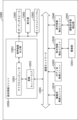
- FIG. 23 is a block diagram showing an example of the configuration of an imaging device as an electronic device to which the technology disclosed herein is applied.
- the imaging device 600 in FIG. 23 comprises an optical section 601 consisting of a group of lenses etc., a solid-state imaging device (imaging device) 602 which employs the configuration of the solid-state imaging device 1 in FIG. 1, and a DSP (Digital Signal Processor) circuit 603 which is a camera signal processing circuit.
- the imaging device 600 also comprises a frame memory 604, a display section 605, a recording section 606, an operation section 607, and a power supply section 608.
- the DSP circuit 603, frame memory 604, display section 605, recording section 606, operation section 607, and power supply section 608 are interconnected via a bus line 609.
- the optical unit 601 takes in incident light (image light) from a subject and forms an image on the imaging surface of the solid-state imaging device 602.
- the solid-state imaging device 602 converts the amount of incident light imaged on the imaging surface by the optical unit 601 into an electrical signal on a pixel-by-pixel basis and outputs it as a pixel signal.
- This solid-state imaging device 602 uses the solid-state imaging device 1 of FIG. 1, that is, a solid-state imaging device in which the planar shape of the pixel separation section 71 is an approximately rectangular planar shape for the first separation wall 71a close to the front surface side of the semiconductor substrate 51 and an approximately circular or approximately octagonal planar shape for the second separation wall 71b deeper than that.
- the display unit 605 is composed of a thin display such as an LCD (Liquid Crystal Display) or an organic EL (Electro Luminescence) display, and displays moving images or still images captured by the solid-state imaging device 602.
- the recording unit 606 records the moving images or still images captured by the solid-state imaging device 602 on a recording medium such as a hard disk or semiconductor memory.
- the operation unit 607 issues operation commands for the various functions of the imaging device 600 under the operation of the user.
- the power supply unit 608 appropriately supplies various types of power to these devices as operating power sources for the DSP circuit 603, frame memory 604, display unit 605, recording unit 606, and operation unit 607.
- the transfer design of the photodiode PD can be simplified and the saturation charge amount Qs can be increased. Therefore, high-quality captured images can be obtained even in the imaging device 600 such as a video camera, a digital still camera, and even a camera module for mobile devices such as a mobile phone.
- the technology according to the present disclosure can be applied to various products.
- the technology according to the present disclosure may be realized as a device mounted on any type of moving body such as an automobile, an electric vehicle, a hybrid electric vehicle, a motorcycle, a bicycle, a personal mobility device, an airplane, a drone, a ship, or a robot.
- FIG. 24 is a block diagram showing a schematic configuration example of a vehicle control system, which is an example of a mobile object control system to which the technology disclosed herein can be applied.
- the vehicle control system 12000 includes a plurality of electronic control units connected via a communication network 12001.
- the vehicle control system 12000 includes a drive system control unit 12010, a body system control unit 12020, an outside vehicle information detection unit 12030, an inside vehicle information detection unit 12040, and an integrated control unit 12050.
- Also shown as functional components of the integrated control unit 12050 are a microcomputer 12051, an audio/video output unit 12052, and an in-vehicle network I/F (interface) 12053.
- the drive system control unit 12010 controls the operation of devices related to the drive system of the vehicle according to various programs.
- the drive system control unit 12010 functions as a control device for a drive force generating device for generating the drive force of the vehicle, such as an internal combustion engine or a drive motor, a drive force transmission mechanism for transmitting the drive force to the wheels, a steering mechanism for adjusting the steering angle of the vehicle, and a braking device for generating a braking force for the vehicle.
- the body system control unit 12020 controls the operation of various devices installed in the vehicle body according to various programs.
- the body system control unit 12020 functions as a control device for a keyless entry system, a smart key system, a power window device, or various lamps such as headlamps, tail lamps, brake lamps, turn signals, and fog lamps.
- radio waves or signals from various switches transmitted from a portable device that replaces a key can be input to the body system control unit 12020.
- the body system control unit 12020 accepts the input of these radio waves or signals and controls the vehicle's door lock device, power window device, lamps, etc.
- the outside-vehicle information detection unit 12030 detects information outside the vehicle equipped with the vehicle control system 12000.
- the image capturing unit 12031 is connected to the outside-vehicle information detection unit 12030.
- the outside-vehicle information detection unit 12030 causes the image capturing unit 12031 to capture images outside the vehicle and receives the captured images.
- the outside-vehicle information detection unit 12030 may perform object detection processing or distance detection processing for people, cars, obstacles, signs, characters on the road surface, etc. based on the received images.
- the imaging unit 12031 is an optical sensor that receives light and outputs an electrical signal according to the amount of light received.
- the imaging unit 12031 can output the electrical signal as an image, or as distance measurement information.
- the light received by the imaging unit 12031 may be visible light, or may be invisible light such as infrared light.
- the in-vehicle information detection unit 12040 detects information inside the vehicle.
- a driver state detection unit 12041 that detects the state of the driver is connected.
- the driver state detection unit 12041 includes, for example, a camera that captures an image of the driver, and the in-vehicle information detection unit 12040 may calculate the driver's degree of fatigue or concentration based on the detection information input from the driver state detection unit 12041, or may determine whether the driver is dozing off.
- the microcomputer 12051 can calculate the control target values of the driving force generating device, steering mechanism, or braking device based on the information inside and outside the vehicle acquired by the outside vehicle information detection unit 12030 or the inside vehicle information detection unit 12040, and output a control command to the drive system control unit 12010.
- the microcomputer 12051 can perform cooperative control aimed at realizing the functions of an ADAS (Advanced Driver Assistance System), including avoiding or mitigating vehicle collisions, following based on the distance between vehicles, maintaining vehicle speed, vehicle collision warning, or vehicle lane departure warning.
- ADAS Advanced Driver Assistance System
- the microcomputer 12051 can also perform cooperative control for the purpose of autonomous driving, which allows the vehicle to travel autonomously without relying on the driver's operation, by controlling the driving force generating device, steering mechanism, braking device, etc. based on information about the surroundings of the vehicle acquired by the outside vehicle information detection unit 12030 or the inside vehicle information detection unit 12040.
- the microcomputer 12051 can also output control commands to the body system control unit 12020 based on information outside the vehicle acquired by the outside information detection unit 12030. For example, the microcomputer 12051 can control the headlamps according to the position of a preceding vehicle or an oncoming vehicle detected by the outside information detection unit 12030, and perform cooperative control aimed at preventing glare, such as switching from high beams to low beams.
- the audio/image output unit 12052 transmits at least one output signal of audio and image to an output device capable of visually or audibly notifying the occupants of the vehicle or the outside of the vehicle of information.
- an audio speaker 12061, a display unit 12062, and an instrument panel 12063 are exemplified as output devices.
- the display unit 12062 may include, for example, at least one of an on-board display and a head-up display.
- FIG. 25 shows an example of the installation position of the imaging unit 12031.
- the vehicle 12100 has imaging units 12101, 12102, 12103, 12104, and 12105 as the imaging unit 12031.
- the imaging units 12101, 12102, 12103, 12104, and 12105 are provided, for example, at the front nose, side mirrors, rear bumper, back door, and the top of the windshield inside the vehicle cabin of the vehicle 12100.
- the imaging unit 12101 provided at the front nose and the imaging unit 12105 provided at the top of the windshield inside the vehicle cabin mainly acquire images of the front of the vehicle 12100.
- the imaging units 12102 and 12103 provided at the side mirrors mainly acquire images of the sides of the vehicle 12100.
- the imaging unit 12104 provided at the rear bumper or back door mainly acquires images of the rear of the vehicle 12100.
- the images of the front acquired by the imaging units 12101 and 12105 are mainly used to detect preceding vehicles, pedestrians, obstacles, traffic lights, traffic signs, lanes, etc.
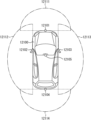
- FIG. 25 shows an example of the imaging ranges of the imaging units 12101 to 12104.
- Imaging range 12111 indicates the imaging range of the imaging unit 12101 provided on the front nose
- imaging ranges 12112 and 12113 indicate the imaging ranges of the imaging units 12102 and 12103 provided on the side mirrors, respectively
- imaging range 12114 indicates the imaging range of the imaging unit 12104 provided on the rear bumper or back door.
- an overhead image of the vehicle 12100 viewed from above is obtained by superimposing the image data captured by the imaging units 12101 to 12104.
- At least one of the imaging units 12101 to 12104 may have a function of acquiring distance information.
- at least one of the imaging units 12101 to 12104 may be a stereo camera consisting of multiple imaging elements, or an imaging element having pixels for phase difference detection.
- the microcomputer 12051 can obtain the distance to each solid object within the imaging ranges 12111 to 12114 and the change in this distance over time (relative speed with respect to the vehicle 12100) based on the distance information obtained from the imaging units 12101 to 12104, and can extract as a preceding vehicle, in particular, the closest solid object on the path of the vehicle 12100 that is traveling in approximately the same direction as the vehicle 12100 at a predetermined speed (e.g., 0 km/h or faster). Furthermore, the microcomputer 12051 can set the inter-vehicle distance that should be maintained in advance in front of the preceding vehicle, and perform automatic braking control (including follow-up stop control) and automatic acceleration control (including follow-up start control). In this way, cooperative control can be performed for the purpose of automatic driving, which runs autonomously without relying on the driver's operation.
- automatic braking control including follow-up stop control
- automatic acceleration control including follow-up start control
- the microcomputer 12051 classifies and extracts three-dimensional object data on three-dimensional objects, such as two-wheeled vehicles, ordinary vehicles, large vehicles, pedestrians, utility poles, and other three-dimensional objects, based on the distance information obtained from the imaging units 12101 to 12104, and can use the data to automatically avoid obstacles.
- the microcomputer 12051 distinguishes obstacles around the vehicle 12100 into obstacles that are visible to the driver of the vehicle 12100 and obstacles that are difficult to see.
- the microcomputer 12051 determines the collision risk, which indicates the risk of collision with each obstacle, and when the collision risk is equal to or exceeds a set value and there is a possibility of a collision, it can provide driving assistance for collision avoidance by outputting an alarm to the driver via the audio speaker 12061 or the display unit 12062, or by performing forced deceleration or avoidance steering via the drive system control unit 12010.
- At least one of the imaging units 12101 to 12104 may be an infrared camera that detects infrared rays.
- the microcomputer 12051 can recognize a pedestrian by determining whether or not a pedestrian is present in the image captured by the imaging units 12101 to 12104. The recognition of such a pedestrian is performed, for example, by a procedure of extracting feature points in the image captured by the imaging units 12101 to 12104 as infrared cameras, and a procedure of performing pattern matching processing on a series of feature points that indicate the contour of an object to determine whether or not it is a pedestrian.
- the audio/image output unit 12052 controls the display unit 12062 to superimpose a rectangular contour line for emphasis on the recognized pedestrian.
- the audio/image output unit 12052 may also control the display unit 12062 to display an icon or the like indicating a pedestrian at a desired position.
- the technology according to the present disclosure can be applied to the imaging unit 12031.
- the solid-state imaging device 1 can be applied as the imaging unit 12031.
- the first conductivity type was P type and the second conductivity type was N type, and electrons were used as the signal charge
- this disclosure can also be applied to a solid-state imaging device in which holes are used as the signal charge.
- the first conductivity type can be N type and the second conductivity type can be P type, and each of the aforementioned semiconductor regions can be configured with a semiconductor region of the opposite conductivity type.
- the technology of the present disclosure can be applied not only to solid-state imaging devices but also to general photodetection devices equipped with pixels that receive incident light and perform photoelectric conversion.
- a light receiving device distance measuring sensor
- a distance measuring system that receives infrared light irradiated as active light and measures the distance to a subject using a direct ToF method or an indirect ToF method.
- the technology of the present disclosure is not limited to application to solid-state imaging devices that detect the distribution of the amount of incident visible light and capture it as an image, but can be applied to solid-state imaging devices that capture the distribution of the amount of incident infrared rays, X-rays, particles, etc. as an image, and in a broad sense, solid-state imaging devices (physical quantity distribution detection devices) such as fingerprint detection sensors that detect the distribution of other physical quantities such as pressure and capacitance and capture it as an image.
- physical quantity distribution detection devices such as fingerprint detection sensors that detect the distribution of other physical quantities such as pressure and capacitance and capture it as an image.
- the photodetection device described in any one of (1) to (3) wherein the planar shape of the pixel separation portion is different when viewed from the first surface side of the semiconductor substrate and when viewed from the second surface side.
- the first surface of the semiconductor substrate is a front surface of the semiconductor substrate;
- the first separation wall has a substantially rectangular planar shape
- the planar shape of the pixel having the photoelectric conversion region is configured to be rectangular, and two pixel regions are configured to be square,
- the photodetection device is either a pixel row in which only green color filters are arranged, a pixel row in which green color filters and red color filters are arranged alternately, or a pixel row in which green color filters and blue color filters are arranged alternately.
- the planar shape of a pixel having the photoelectric conversion region is rectangular, and a square unit pixel formed by two pixel regions in a square shape has a color filter array in which red, green, or blue color filters are arranged in 2 x 2 square unit pixel units.
- the photodetection device according to any one of (1) to (12), wherein the pixel having the photoelectric conversion region is arranged with its pixel position shifted by half a pitch of the pixel size from pixels in other adjacent pixel columns or other pixel rows.
- An electronic device comprising a photodetector device, in which, with respect to a width of the photoelectric conversion region to the second separation wall in a direction perpendicular to a center line that divides the photoelectric conversion region in two horizontally or vertically, a first width at the center of a pixel side is larger than a second width at a portion near a corner of the pixel.
- 1 solid-state imaging device 11 pixel array section, 21 pixel, 51 semiconductor substrate, 51a first surface, 51b second surface, 61 P-type semiconductor region, 62 N-type semiconductor region, 71 pixel separation section, 71a, 71a' first separation wall, 71b, 71b' second separation wall, 72 sidewall, 73 insulating film, 74 P-type semiconductor region, 75 N-type semiconductor region, 81 planarization film, 82 light-shielding film, 241 conductive material, 301 overflow path, 311 On-chip lens, 341 color filter, 600 imaging device, 602 solid-state imaging device, HLb1 first width, HLb2 second width, HUa1 first width, HUa2 second width, VLb1 first width, VLb2 second width, VUa1 first width, VUa2 second width, PD photodiode, RST reset transistor, SEL selection transistor, TG transfer transistor, AMP amplification transistor, FD floating diffusion region
Landscapes
- Engineering & Computer Science (AREA)
- Multimedia (AREA)
- Signal Processing (AREA)
- Solid State Image Pick-Up Elements (AREA)
Abstract
本開示は、画素間分離部を有する画素において光電変換領域内の電荷転送を改善することができるようにする光検出装置および電子機器に関する。 光検出装置は、半導体基板に形成された光電変換領域と、半導体基板を貫通し、光電変換領域を画素毎に分離する画素分離部とを備える。画素分離部は、半導体基板の第1面側の第1分離壁と、半導体基板の第1面と反対の第2面側の第2分離壁とを有し、第1分離壁と第2分離壁の幅は異なり、光電変換領域を水平方向または垂直方向に二分する中心線に対して垂直な方向の光電変換領域の第2分離壁までの幅に関し、画素の辺中央部の第1の幅が、画素の角近傍部の第2の幅より大きく構成される。本開示は、例えば、固体撮像装置や、ToF方式の測距センサ等に適用できる。
Description
本開示は、光検出装置および電子機器に関し、特に、画素間分離部を有する画素において光電変換領域内の電荷転送を改善した光検出装置および電子機器に関する。
従来、隣接する画素間にトレンチを形成し、トレンチの側壁に沿ってアキュムレーション層を形成することで暗電流の発生を抑制した固体撮像装置がある(例えば、特許文献1参照)。また、画素間分離のトレンチの幅を、表面側と裏面側で異なる幅で形成した固体撮像装置がある(例えば、特許文献2参照)。
トレンチの側壁にP型層またはN型層を形成する場合、平面視で画素の角部と辺中央部とでポテンシャル差が生じると、電荷の転送設計が難しくなる。
本開示は、このような状況に鑑みてなされたものであり、画素間分離部を有する画素において光電変換領域内の電荷転送を改善することができるようにするものである。
本開示の第1の側面の光検出装置は、
半導体基板に形成された光電変換領域と、
前記半導体基板を貫通し、前記光電変換領域を画素毎に分離する画素分離部と
を備え、
前記画素分離部は、前記半導体基板の第1面側の第1分離壁と、前記半導体基板の第1面と反対の第2面側の第2分離壁とを有し、
前記第1分離壁と前記第2分離壁の幅は異なり、
前記光電変換領域を水平方向または垂直方向に二分する中心線に対して垂直な方向の前記光電変換領域の前記第2分離壁までの幅に関し、画素の辺中央部の第1の幅が、画素の角近傍部の第2の幅より大きく構成された
を備える。
半導体基板に形成された光電変換領域と、
前記半導体基板を貫通し、前記光電変換領域を画素毎に分離する画素分離部と
を備え、
前記画素分離部は、前記半導体基板の第1面側の第1分離壁と、前記半導体基板の第1面と反対の第2面側の第2分離壁とを有し、
前記第1分離壁と前記第2分離壁の幅は異なり、
前記光電変換領域を水平方向または垂直方向に二分する中心線に対して垂直な方向の前記光電変換領域の前記第2分離壁までの幅に関し、画素の辺中央部の第1の幅が、画素の角近傍部の第2の幅より大きく構成された
を備える。
本開示の第2の側面の電子機器は、
半導体基板に形成された光電変換領域と、
前記半導体基板を貫通し、前記光電変換領域を画素毎に分離する画素分離部と
を備え、
前記画素分離部は、前記半導体基板の第1面側の第1分離壁と、前記半導体基板の第1面と反対の第2面側の第2分離壁とを有し、
前記第1分離壁と前記第2分離壁の幅は異なり、
前記光電変換領域を水平方向または垂直方向に二分する中心線に対して垂直な方向の前記光電変換領域の前記第2分離壁までの幅に関し、画素の辺中央部の第1の幅が、画素の角近傍部の第2の幅より大きく構成された
光検出装置
を備える。
半導体基板に形成された光電変換領域と、
前記半導体基板を貫通し、前記光電変換領域を画素毎に分離する画素分離部と
を備え、
前記画素分離部は、前記半導体基板の第1面側の第1分離壁と、前記半導体基板の第1面と反対の第2面側の第2分離壁とを有し、
前記第1分離壁と前記第2分離壁の幅は異なり、
前記光電変換領域を水平方向または垂直方向に二分する中心線に対して垂直な方向の前記光電変換領域の前記第2分離壁までの幅に関し、画素の辺中央部の第1の幅が、画素の角近傍部の第2の幅より大きく構成された
光検出装置
を備える。
本開示の第1及び第2の側面においては、半導体基板に形成された光電変換領域と、前記半導体基板を貫通し、前記光電変換領域を画素毎に分離する画素分離部とが設けられ、前記画素分離部は、前記半導体基板の第1面側の第1分離壁と、前記半導体基板の第1面と反対の第2面側の第2分離壁とを有し、前記第1分離壁と前記第2分離壁の幅は異なり、前記光電変換領域を水平方向または垂直方向に二分する中心線に対して垂直な方向の前記光電変換領域の前記第2分離壁までの幅に関し、画素の辺中央部の第1の幅が、画素の角近傍部の第2の幅より大きく構成される。
光検出装置及び電子機器は、独立した装置であっても良いし、他の装置に組み込まれるモジュールであっても良い。
以下、添付図面を参照しながら、本開示の技術を実施するための形態(以下、実施の形態という)について説明する。説明は以下の順序で行う。
1.固体撮像装置の概略構成例
2.画素の回路構成例
3.画素の第1構造例
4.第1構造例の画素分離部の形成方法
5.画素の第2構造例
6.画素の変形例
7.長方形画素の千鳥配置
8.イメージセンサの使用例
9.電子機器への適用例
10.移動体への応用例
1.固体撮像装置の概略構成例
2.画素の回路構成例
3.画素の第1構造例
4.第1構造例の画素分離部の形成方法
5.画素の第2構造例
6.画素の変形例
7.長方形画素の千鳥配置
8.イメージセンサの使用例
9.電子機器への適用例
10.移動体への応用例
以下の説明で参照する図面において、同一又は類似の部分には同一又は類似の符号を付すことにより重複説明を適宜省略する。図面は模式的なものであり、厚みと平面寸法との関係、各層の厚みの比率等は実際のものとは異なる。また、図面相互間においても、互いの寸法の関係や比率が異なる部分が含まれている場合がある。
また、以下の説明における上下等の方向の定義は、単に説明の便宜上の定義であって、本開示の技術的思想を限定するものではない。例えば、対象を90°回転して観察すれば上下は左右に変換して読まれ、180°回転して観察すれば上下は反転して読まれる。
本開示の技術は、画素が行列状に2次元配置された画素アレイ部を有し、入射光を光電変換して光量に応じた画素信号を出力する光検出装置全般に適用することができる。例えば、本開示の技術は、入射光の光量に応じた撮像信号を生成して出力する固体撮像装置や、アクティブ光として照射された赤外光を受光し、direct ToF方式またはindirect ToF方式により被写体までの距離を測定する測距システムの受光装置(測距センサ)などに適用することができる。以下では、本開示の技術を、CMOSイメージセンサとも呼ばれるX-Yアドレス方式の固体撮像装置に適用した例を説明する。
<1.固体撮像装置の概略構成例>
図1は、本開示の実施の形態に係る固体撮像装置の概略構成を示す図である。
図1は、本開示の実施の形態に係る固体撮像装置の概略構成を示す図である。
図1の固体撮像装置1は、画素アレイ部11と周辺回路部とを備える。周辺回路部は、例えば、垂直駆動部12、カラム処理部13、水平駆動部14、及び、システム制御部15を備える。
固体撮像装置1は、さらに、信号処理部16及びデータ格納部17を備えている。信号処理部16及びデータ格納部17は、画素アレイ部11、垂直駆動部12等と同じ基板上に搭載しても構わないし、別の基板上に配置するようにしても構わない。また、信号処理部16及びデータ格納部17は、固体撮像装置1とは別の半導体チップに設けてもよい。
画素アレイ部11は、複数の画素21が行方向及び列方向の行列状に2次元配置された構成となっている。ここで、行方向とは、画素アレイ部11の画素行、すなわち水平方向の配列方向を言い、列方向とは、画素アレイ部11の画素列、すなわち垂直方向の配列方向を言う。
画素21は、受光した光量に応じた電荷を生成しかつ蓄積する光電変換部と、複数の画素トランジスタ(いわゆるMOSトランジスタ)を有する。なお、画素21の具体的回路構成例については、図2等を参照して後述する。
また、画素アレイ部11において、画素行ごとに行信号線としての画素駆動線22が行方向に沿って配線され、画素列ごとに列信号線としての垂直信号線23が列方向に沿って配線されている。画素駆動線22は、画素21から信号を読み出す際の駆動を行うための駆動信号を伝送する。図1では、画素駆動線22について1本の配線として示しているが、1本に限られるものではない。画素駆動線22の一端は、垂直駆動部12の各行に対応した出力端に接続されている。
垂直駆動部12は、シフトレジスタやアドレスデコーダなどによって構成され、画素アレイ部11の各画素を全画素同時あるいは行単位等で駆動する。垂直駆動部12は、システム制御部15とともに、画素アレイ部11の各画素の動作を制御する駆動部を構成している。垂直駆動部12は、具体的な構成については図示を省略するが、一般的に、読出し走査系と掃出し走査系の2つの走査系を有する。
読出し走査系は、画素21から信号を読み出すために、画素アレイ部11の画素21を行単位で順に選択走査する。画素21から読み出される信号はアナログ信号である。掃出し走査系は、読出し走査系によって読出し走査が行われる読出し行に対して、その読出し走査よりも露光時間分だけ先行して掃出し走査を行う。
この掃出し走査系による掃出し走査により、読出し行の画素21の光電変換部から不要な電荷が掃き出されることによって各画素21の光電変換部がリセットされる。そして、この掃出し走査系による不要電荷を掃き出す(リセットする)ことにより、所謂電子シャッタ動作が行われる。ここで、電子シャッタ動作とは、光電変換部の電荷を捨てて、新たに露光を開始する(電荷の蓄積を開始する)動作のことを言う。
読出し走査系による読出し動作によって読み出される信号は、その直前の読出し動作または電子シャッタ動作以降に受光した光量に対応するものである。そして、直前の読出し動作による読出しタイミングまたは電子シャッタ動作による掃出しタイミングから、今回の読出し動作による読出しタイミングまでの期間が、画素21における露光期間となる。
垂直駆動部12によって選択走査された画素行の各画素21から出力される信号は、画素列ごとに垂直信号線23の各々を通してカラム処理部13に入力される。カラム処理部13は、画素アレイ部11の画素列ごとに、選択行の各画素21から垂直信号線23を通して出力される信号に対して所定の信号処理を行うとともに、信号処理後の画素信号を一時的に保持する。
具体的には、カラム処理部13は、信号処理として少なくとも、ノイズ除去処理、例えばCDS(Correlated Double Sampling;相関二重サンプリング)処理を行う。CDS処理により、リセットノイズや画素内の増幅トランジスタの閾値ばらつき等の画素固有の固定パターンノイズが除去される。カラム処理部13には、ノイズ除去処理以外に、例えば、AD(アナログ-デジタル)変換機能を持たせ、アナログの画素信号をデジタル信号に変換して出力することも可能である。
水平駆動部14は、シフトレジスタやアドレスデコーダなどによって構成され、カラム処理部13の画素列に対応する単位回路を順番に選択する。この水平駆動部14による選択走査により、カラム処理部13において単位回路ごとに信号処理された画素信号が順番に出力される。
システム制御部15は、各種のタイミング信号を生成するタイミングジェネレータなどによって構成され、タイミングジェネレータで生成された各種のタイミングを基に、垂直駆動部12、カラム処理部13、及び、水平駆動部14などの駆動制御を行う。
信号処理部16は、少なくとも演算処理機能を有し、カラム処理部13から出力される画素信号に対して演算処理等の種々の信号処理を行う。データ格納部17は、信号処理部16での信号処理に当たって、その処理に必要なデータを一時的に格納する。信号処理部16において信号処理された画素信号は、所定のフォーマットに変換され、出力部18から装置外部へ出力される。
<2.画素の回路構成例>
図2は、画素アレイ部11に行列状に2次元配置された各画素21の回路構成例を示している。
図2は、画素アレイ部11に行列状に2次元配置された各画素21の回路構成例を示している。
各画素21は、例えば図2に示されるように、各画素の信号を読み出す読み出し回路を、行方向および列方向に2画素ずつの2x2の4画素で共有する共有画素構造を有している。
具体的には、画素アレイ部11において、光電変換部としてのフォトダイオードPDと転送トランジスタTGは画素単位に設けられ、浮遊拡散領域FD、リセットトランジスタRST、増幅トランジスタAMP、および、選択トランジスタSELは、共有単位である4画素で共有して使用される。転送トランジスタTG、リセットトランジスタRST、増幅トランジスタAMP、および、選択トランジスタSELの各画素トランジスタは、いずれも、N型のMOSトランジスタ(MOS FET)で構成され、読み出し回路を構成する。
図面では、読み出し回路を共有する4画素のフォトダイオードPDと転送トランジスタTGとを区別するため、フォトダイオードPD1乃至PD4、及び、転送トランジスタTG1乃至TG4のように1乃至4の数字が付加されている。
フォトダイオードPDは、受光した光量に応じた電荷(信号電荷)を生成し、蓄積する。フォトダイオードPDは、アノード端子が接地されているとともに、カソード端子が転送トランジスタTGを介して、浮遊拡散領域FDに接続されている。
転送トランジスタTGは、ゲート電極に供給される転送駆動信号によりオンされたとき、フォトダイオードPDで生成された電荷を読み出し、浮遊拡散領域FDに転送する。浮遊拡散領域FDは、4個のフォトダイオードPDの少なくとも1つから読み出された電荷を保持する。
リセットトランジスタRSTは、ゲート電極に供給されるリセット駆動信号によりオンされたとき、浮遊拡散領域FDに蓄積されている電荷がドレイン(電源電圧VDD)に排出され、浮遊拡散領域FDの電位をリセットする。
増幅トランジスタAMPは、浮遊拡散領域FDの電位に応じた信号を出力する。すなわち、増幅トランジスタAMPは、垂直信号線23を介して接続されている定電流源としての負荷MOSトランジスタ(不図示)とソースフォロア回路を構成し、浮遊拡散領域FDに蓄積されている電荷に応じたレベルを示す信号VSLが、増幅トランジスタAMPから選択トランジスタSELを介してカラム処理部13(図1)に出力される。
選択トランジスタSELは、ゲート電極に供給される選択駆動信号により共有単位が選択されたときオンされ、共有単位の各画素21で生成された信号VSLを、垂直信号線23を介してカラム処理部13に出力する。転送駆動信号、選択駆動信号、及びリセット駆動信号は、図1の画素駆動線22を介して垂直駆動部12から供給される。
共有単位の2x2の4個の画素21は、以上のように、リセットトランジスタRST、増幅トランジスタAMP、および、選択トランジスタSELの各画素トランジスタを共有して使用する。
固体撮像装置1は、例えば、動作モードに応じて、次のような駆動を適宜選択して行うことができる。
例えば、固体撮像装置1は、第1の動作モードとして、共有単位の4画素の転送トランジスタTGを1画素単位で順番にオンし、1画素のフォトダイオードPDで生成された電荷を浮遊拡散領域FDに転送し、信号VSLとして、垂直信号線23を介してカラム処理部13に出力するモードが可能である。
例えば、固体撮像装置1は、第2の動作モードとして、共有単位の4画素のうち、行方向または列方向に隣接する2画素単位で転送トランジスタTGをオンし、2画素のフォトダイオードPDで生成された電荷を同時に浮遊拡散領域FDに転送し、信号VSLとして、垂直信号線23を介してカラム処理部13に出力するモードが可能である。
例えば、固体撮像装置1は、第3の動作モードとして、共有単位の4画素全ての転送トランジスタTGを同時にオンし、4画素のフォトダイオードPDで生成された電荷を同時に浮遊拡散領域FDに転送し、信号VSLとして、垂直信号線23を介してカラム処理部13に出力するモードが可能である。
なお、各画素21が読み出し回路を共有する共有単位は4画素に限定されない。例えば、4x2または2x4の8画素で読み出し回路を共有する回路構成を採用してもよい。勿論、各画素21は、読み出し回路を共有せずに、画素単位に個別に設ける構成も取り得る。
<3.画素の第1構造例>
図3は、画素21の第1構造例を示す断面図である。
図3は、画素21の第1構造例を示す断面図である。
以下に説明する画素21は、裏面照射型である場合を例に挙げて説明を行うが、本技術は表面照射型に対しても適用することができる。
図3に示される画素21は、半導体材料として例えばシリコン(Si)を用いた半導体基板51に形成されている。図3において半導体基板51の上側の第1面51aは、半導体基板51のおもて面であり、第1面51aには、転送トランジスタTG、増幅トランジスタAMP、リセットトランジスタRST等の画素トランジスタと、多層配線層が形成されているが、図示が省略されている。多層配線層は、例えば、銅(Cu)、タングステン(W)、アルミニウム(Al)等の金属材料からなる配線と、シリコン酸化膜等からなる層間絶縁膜とを1層以上含む層である。一方、半導体基板51の下側の第2面51bが、半導体基板51の裏面であり、光が入射される光入射面である。
半導体基板51には、第1面51a側に形成されたP型半導体領域61と、第2面51b側に形成されたN型半導体領域62が画素毎に形成され、P型半導体領域61とN型半導体領域62とによるPN接合を利用したフォトダイオードPDが構成されている。P型半導体領域61とN型半導体領域62は、画素21の光電変換領域の一部である。
また、半導体基板51の隣接する画素21どうしの境界部には、画素毎に形成された光電変換領域を画素単位に分離する画素分離部71が形成されている。画素分離部71は、異なる幅の第1分離壁71aと第2分離壁71bとで構成され、半導体基板51を貫通して、画素毎に形成された光電変換領域を完全分離している。具体的には、半導体基板51のおもて面側の第1分離壁71aの幅が、裏面側の第2分離壁71bの幅よりも大きく形成されている(第1分離壁71aの幅>第2分離壁71bの幅)。第1分離壁71aは、サイドウォール72と絶縁膜73とを埋め込むことにより構成され、第2分離壁71bは、絶縁膜73のみを埋め込むことにより構成されている。サイドウォール72は、酸化膜(SiO2)、窒化膜(SiN)、または、それらの積層で形成されている。絶縁膜73は、例えば、SiO2、SiN、アンドープドポリシリコン、Al2O3などで形成されている。
第2分離壁71bの側壁には、画素21の中心側(内側)へ向かって、P型半導体領域74、N型半導体領域75が、その順番で形成されている。P型半導体領域74とN型半導体領域75も画素21の光電変換領域の一部である。N型半導体領域62とN型半導体領域75は不純物濃度が異なり、N型半導体領域75は、N型半導体領域62よりも高濃度な領域とされている。P型半導体領域74は、第2分離壁71bの側壁に沿って高濃度で形成されることにより、第2分離壁71bの界面からの電子を抑制する。また、高濃度のP型半導体領域74の内側(画素中心側)に高濃度のN型半導体領域75を形成することにより、飽和電荷量Qsを増大させることができる。P型半導体領域74とN型半導体領域75は、例えば、コンフォーマルドーピングにより形成される。コンフォーマルドーピングは、例えば、固相拡散法や、プラズマドーピング法などを含む不純物領域形成方法である。
半導体基板51の光入射面である第2面51b上には、平坦化膜81が形成されている。平坦化膜81内部の画素境界部には、遮光膜82が形成されている。遮光膜82は、隣接する画素21への光の漏れ込みを防止するために設けられている。遮光膜82は、例えば、W(タングステン)等の金属材料から成る。
平坦化膜81のさらに外側には、入射光をフォトダイオードPDに集光させるOCL(オンチップレンズ)83が形成されている。OCL83は、無機材料で形成することができ、例えば、SiN、SiO、SiOxNy(ただし、0<x≦1、0<y≦1である)を用いることができる。
図3では図示していないが、OCL83にカバーガラスや、樹脂などの透明板が接着されている構成とすることもできる。また、図3では図示していないが、OCL83と平坦化膜81との間にカラーフィルタ層を形成した構成としても良い。カラーフィルタ層を形成した場合のカラーフィルタ配列は、例えば、2×2の4画素に、R(赤),G(緑),G(緑),B(青)のカラーフィルタを配置したベイヤ配列や、1色の配置単位を2×2の4画素として、2×2の4画素単位でR,G,G,Bのカラーフィルタをベイヤ配列で配置したクワッドベイヤ配列で配列することができる。
以上のように、画素21は、半導体基板51の深さ位置によって異なる幅で形成された第1分離壁71aと第2分離壁71bとからなる画素分離部71を有する。第1分離壁71aと第2分離壁71bは、異なる平面形状で構成されている。
図4は、第1分離壁71aと第2分離壁71bの平面形状を模式的に示した平面図である。
図4の第1分離壁71a’は、図3のX-X’線における第1分離壁71aとN型半導体領域62との境界を示している。図4の第2分離壁71b’は、図3のY-Y’線における第2分離壁71bとP型半導体領域74との境界を示している。
第1分離壁71a’は、半導体基板51のおもて面である第1面51a側の画素分離部71と光電変換領域との境界であり、第2分離壁71b’は、半導体基板51の裏面である第2面51b側の画素分離部71と光電変換領域との境界である。したがって、画素21は、画素分離部71の平面形状が、半導体基板51のおもて面側からみた場合と、裏面側からみた場合とで異なるように形成されている。
第1分離壁71a’は、光電変換領域の角部を除いて直線的に形成されており、略矩形の平面形状を有している。一方、第2分離壁71b’は、略円形の平面形状を有している。隣接する画素21の第1分離壁71a’間の幅DSaは、第2分離壁71b’間の幅DSbよりも大きい(幅広である)。画素分離部71の製造方法については後述するが、このような平面形状の違いは、製造工程において、サイドウォール72の有無と、水素ベーク処理(H2 Bake)を行った際の半導体層(Si)のマイグレーションによって発生する。
画素21の光電変換領域を水平方向(図4において左右方向)に二分する線を中心線101hとして、中心線101hに対して垂直な方向の光電変換領域の第1分離壁71a’までの幅HUaを、光電変換領域の辺中央部と角近傍部で比較すると、辺中央部の第1分離壁71a’までの第1の幅HUa1と、角近傍部の第1分離壁71a’までの第2の幅HUa2とは略同一である(第1の幅HUa1=第2の幅HUa2)。
一方、中心線101hに対して垂直な方向の光電変換領域の第2分離壁71b’までの幅HLbを、画素21の辺中央部と角近傍部で比較すると、辺中央部の第2分離壁71b’までの第1の幅HLb1が、角近傍部の第2分離壁71b’までの第2の幅HLb2よりも大きい(第1の幅HLb1>第2の幅HLb2)。光電変換領域の辺中央部の第1分離壁71a’までの第1の幅HUa1と、第2分離壁71b’までの第1の幅HLb1とを比較すると、辺中央部の第2分離壁71b’までの第1の幅HLb1が、第1分離壁71a’までの第1の幅HUa1よりも大きい(第1の幅HLb1>第1の幅HUa1)。中心線101hに対して垂直な方向の光電変換領域の幅HLbは、光電変換領域の辺中央部から角近傍部へ向かうに従い(第1の幅HLb1→第2の幅HLb2)、徐々に小さくなっている。光電変換領域の角近傍部において、第1分離壁71a’までの第2の幅HUa2と、第2分離壁71b’までの第2の幅HLb2とを比較すると、第2分離壁71b’までの第2の幅HLb2が、第1分離壁71a’までの第2の幅HUa2よりも小さい(第2の幅HLb2<第2の幅HUa2)。
このような幅の大小関係は、光電変換領域を垂直方向(図4において上下方向)に二分する線を中心線101vとして、中心線101vに対して垂直な方向の光電変換領域の辺中央部と角近傍部の幅についても同様に言うことができる。すなわち、中心線101vに対して垂直な方向の光電変換領域の第1分離壁71a’までの幅VUaを、光電変換領域の辺中央部と角近傍部で比較すると、辺中央部の第1分離壁71a’までの第1の幅VUa1と、角近傍部の第1分離壁71a’までの第2の幅VUa2とは略同一である(第1の幅VUa1=第2の幅VUa2)。
一方、中心線101vに対して垂直な方向の光電変換領域の第2分離壁71b’までの幅VLbを、光電変換領域の辺中央部と角近傍部で比較すると、辺中央部の第2分離壁71b’までの第1の幅VLb1が、角近傍部の第2分離壁71b’までの第2の幅VLb2よりも大きい(第1の幅VLb1>第2の幅VLb2)。光電変換領域の辺中央部の第1分離壁71a’までの第1の幅VUa1と、第2分離壁71b’までの第1の幅VLb1とを比較すると、第2分離壁71b’までの第1の幅VLb1が、第1分離壁71a’までの第1の幅VUa1よりも大きい(第1の幅VLb1>第1の幅VUa1)。中心線101vに対して垂直な方向の光電変換領域の幅VLbは、光電変換領域の辺中央部から角近傍部へ向かうに従い(第1の幅VLb1→第2の幅VLb2)、徐々に小さくなっている。光電変換領域の角近傍部において、第1分離壁71a’までの第2の幅VUa2と、第2分離壁71b’までの第2の幅VLb2とを比較すると、第1分離壁71a’までの第2の幅VUa2が、第2分離壁71b’までの第2の幅VLb2よりも大きい(第2の幅VUa2>第2の幅VLb2)。
図5は、画素21の第1構造例の変形例であって、図4と同様に第1分離壁71aと第2分離壁71bの平面形状を模式的に示した平面図である。
製造時の条件によっては、図5に示されるように、第2分離壁71b’の平面形状が、略円形というより、略八角形に近い形状となる場合もある。この場合においても、光電変換領域を垂直方向または水平方向に二分する中心線101hまたは101vを基準とする幅HUa(HUa1,HUa2)、幅HUb(HUb1,HUb2)、幅VUa(VUa1,VUa2)、及び、幅VUb(VUb1,VUb2)は、上述した関係を有している。中心線101hに対して垂直な方向の光電変換領域の幅HLbは、光電変換領域の辺中央部から角近傍部へ向かうに従い(第1の幅HLb1→第2の幅HLb2)、辺中央部と同じか、それより小さい幅となっている。中心線101vに対して垂直な方向の光電変換領域の幅VLbは、光電変換領域の辺中央部から角近傍部へ向かうに従い(第1の幅VLb1→第2の幅VLb2)、辺中央部と同じか、それより小さい幅となっている。
以上のように、第1構造例に係る画素21は、各画素の光電変換領域を完全分離する画素分離部71の平面形状として、半導体基板51のおもて面である第1面51a側に近い第1分離壁71aでは略矩形の平面形状を有し、それよりも深い第2分離壁71bでは略円形または略八角形の平面形状を有することを特徴とする。
図6を参照して、第2分離壁71bの平面形状が略矩形状ではなく、略円形状に形成されている場合の効果について説明する。
図6のAは、画素分離部71の第2分離壁71bで分離された光電変換領域が仮に矩形状で形成された場合の光電変換領域の平面図とポテンシャル図を示している。
図6のBは、画素分離部71の第2分離壁71bで分離された光電変換領域が円形状で形成された場合の光電変換領域の平面図とポテンシャル図を示している。
P型半導体領域74とN型半導体領域75は、第2分離壁71bに沿ってコンフォーマルドーピングによって形成される。コンフォーマルドーピングによりP型半導体領域74とN型半導体領域75を形成する際、図6のAの光電変換領域の角部においては、第2分離壁71bの水平方向からのドーピングと、垂直方向からのドーピングとが2重に行われる。そのため、矢印121Xで示される、角部から画素中心方向に向かうポテンシャル121Xpと、矢印121Yで示される、辺中央部から画素中心方向に向かうポテンシャル121Ypとを比較すると、角部にポテンシャルが深い領域が形成される。ポテンシャル121Xpとポテンシャル121Ypとが異なる結果、電荷の転送設計が難しくなる。
これに対して、図6のBのように光電変換領域が円形状で形成された場合、第2分離壁71bからのコンフォーマルドーピングがどの側壁からも均等に行われるため、角部から画素中心方向に向かうポテンシャル121Xpと、辺中央部から画素中心方向に向かうポテンシャル121Ypとが均一になる。ポテンシャル121Xpとポテンシャル121Ypとが均一になることにより、電荷の転送設計が容易になり、相対的に画素21の飽和電荷量Qsを上げる設計も可能となる。
以上のように、第1構造例に係る画素21は、画素分離部71の平面形状として、半導体基板51のおもて面側に近い第1分離壁71aでは略矩形の平面形状を有し、それよりも深い第2分離壁71bでは略円形または略八角形の平面形状を有することにより、光電変換領域内の電荷転送を改善することができる。一方で、半導体基板51のおもて面側は転送トランジスタTGや浮遊拡散領域FDを形成するため直線状であることが好ましく、第1分離壁71aの平面形状が略矩形状であるため好適である。
<4.第1構造例の画素分離部の形成方法>
図7ないし図9を参照して、第1構造例に係る画素21の画素分離部71の形成方法を説明する。図7及び図8では、画素アレイ部11の水平方向または垂直方向に並ぶ3つの画素分離部71を形成する際の断面図が示されている。
図7ないし図9を参照して、第1構造例に係る画素21の画素分離部71の形成方法を説明する。図7及び図8では、画素アレイ部11の水平方向または垂直方向に並ぶ3つの画素分離部71を形成する際の断面図が示されている。
初めに、図7のAに示されるように、SiN、SiO2等を用いたハードマスク201が、半導体基板51のおもて面である第1面51aの所定の領域に形成される。ハードマスク201が形成される領域は、画素分離部71の第1分離壁71aを形成する領域以外の領域である。そして、ハードマスク201に基づいて半導体基板51の一部がドライエッチングによりに除去され、第1分離壁71aに対応する深さのトレンチ202が形成される。トレンチ202の平面形状は、画素境界部に沿った格子状となる。
次に、図7のBに示されるように、トレンチ202の側壁にサイドウォール72が形成される。サイドウォール72は、例えば、CVD,ALD等により酸化膜、窒化膜などを積層した後、それらをRIE法でエッチバックすることにより形成することができる。
次に、図7のCに示されるように、ハードマスク201及びサイドウォール72をマスクとしてドライエッチングを行うことにより、第2分離壁71bに対応する深さのトレンチ203が形成される。トレンチ203の平面形状は、図9のAのようになる。
次に、図7のDに示されるように、P(リン)等のN型の不純物を用いたコンフォーマルドーピングにより、N型半導体領域75がトレンチ203の側壁に形成される。コンフォーマルドーピングとしては、例えば、固相拡散法や、プラズマドーピング法など用いることができる。
続いて、図8のAに示されるように、イン・サイチュー(in-situ)で水素ベーク処理(H2 Bake)が行われる。水素ベーク処理により、サイドウォール72で覆われていないトレンチ203の側壁近傍の半導体基板51のシリコン層はマイグレーションし、半導体基板51のおもて面側から深い部分の第2分離壁71bとなるトレンチ203の平面形状は、図9のBの破線で示されるように、略円形状または略八角形状の平面形状になる。水素ベーク処理が不足すると、半導体基板51のシリコン層と、次の工程においてエピタキシャル成長で形成するシリコン層221との界面に、残存自然酸化膜などにより筋欠陥が発生し、Dark特性が悪化する。
次に、図8のBに示されるように、エピタキシャル成長を用いて、トレンチ203の側壁にシリコン層221が形成される。そのシリコン層221に対して、B(ボロン)等のP型の不純物を用いたコンフォーマルドーピングを行うことにより、図8のCに示されるように、P型半導体領域74がトレンチ203の側壁に形成される。
最後に、図8のDに示されるように、例えば、SiO2、SiN等の絶縁膜73がトレンチ203の内部に埋め込まれることにより、画素分離部71を構成する第1分離壁71aと第2分離壁71bが完成する。その後、半導体基板51の裏面側である第2面51bが、第2分離壁71bが露出する厚さまで薄肉化される。
第1構造例の画素分離部71は、以上のようにして形成することができる。
<5.画素の第2構造例>
図10は、画素21の第2構造例を示す断面図である。
図10は、画素21の第2構造例を示す断面図である。
図10において、図3で示した第1構造例と共通する部分については同一の符号を付してあり、その部分の説明は省略し、異なる部分について説明する。
図10の第2構造例は、画素分離部71を構成する第1分離壁71aと第2分離壁71bの真ん中に、絶縁膜73ではなく、導電性材料241が埋め込まれ、所定のバイアス電圧(例えば負バイアス)が印加される点で第1構造例と相違し、その他の点で共通する。導電性材料241は、例えば、ポリシリコン、N型不純物またはP型不純物がドーピングされたドーピングポリシリコン、ITO(インジウム錫オキサイド)やZnOなどの透明電極等で構成される。画素分離部71の一部として導電性材料241が埋め込まれ、所定のバイアス電圧(例えば負バイアス)を印加することにより、画素分離部71の側壁のピニングを強化することができ、Dark特性を改善することができる。
なお、図10の第2分離壁71bでは、導電性材料241とP型半導体領域74との間には絶縁膜73が形成されていないが、第1分離壁71aと同様に絶縁膜73が形成されてもよい。この場合、第2分離壁71bは、平面視で絶縁膜73で挟まれた中央部に導電性材料241を埋め込んで構成される。
図11は、画素分離部71の一部である導電性材料241の平面形状を模式的に示した平面図である。
図10のX-X’線における第1分離壁71aの導電性材料241は、実線で示されるように略矩形の平面形状を有し、図10のY-Y’線における第2分離壁71bの導電性材料
241は、破線で示されるように略円形の平面形状を有する。
241は、破線で示されるように略円形の平面形状を有する。
図12を参照して、画素分離部71の一部として導電性材料241を埋め込んだ場合に、第2分離壁71bの平面形状が略円形状に形成されている場合の効果について説明する。
画素分離部71の導電性材料241の平面形状が、仮に図12のAに示されるように矩形状で形成された場合、負バイアスが印加された導電性材料241からの電界が、水平方向の辺(側壁)と垂直方向の辺(側壁)の両方から発生するため、光電変換領域の角部で電界が集中し、TDDB(Time Dependent Dielectric Breakdown)寿命の悪化など、信頼性上のウィークスポットとなる。図12のBに示されるように、導電性材料241の平面形状を円形状に形成した場合、導電性材料241による電界が均一となるため、平面形状が円形状に近くなることにより電界集中が緩和され、耐圧性が向上する。したがって、画素分離部71の一部としての導電性材料241の平面形状を略円形状または略八角形状とすることで、固体撮像装置1の信頼性を向上させることができる。
以上のように、第2構造例に係る画素21によれば、第1構造例における光電変換領域内の電荷転送の改善に加えて、信頼性を向上させることができる。
<6.画素の変形例>
図13は、画素21の変形例を示す平面図である。
図13は、画素21の変形例を示す平面図である。
上述した画素21の第1構造例及び第2構造例は、図13のAに示されるように、光電変換領域であるフォトダイオードPDの平面形状を正方形状とした画素構造である。
しかしながら、上述した画素分離部71の構造は、図13のB及びCに示されるような、光電変換領域であるフォトダイオードPDの平面形状が長方形状であるような画素構造についても適用可能である。
図13のB及びCは、フォトダイオードPDの平面形状が長方形状であり、左右に並ぶ2つのフォトダイオードPDの間に、オーバーフローパス301が形成された構造を示している。図13のBは、フォトダイオードPDの周囲が絶縁膜73で構成された第1構造例の画素分離部71に対応し、図13のCは、フォトダイオードPDの周囲に導電性材料241を形成した第2構造例の画素分離部71に対応する。
このようにフォトダイオードPDの平面形状が長方形状であり、左右に並ぶ2つのフォトダイオードPDの間に、オーバーフローパス301が形成された画素構造は、図14に示されるように各画素21の平面形状が長方形状で構成され、行方向に隣接する2個の画素領域で正方形状とされる。そして、正方形状とされた2画素に対して、1つのオンチップレンズ311が配置される。各画素21は、2x2の4画素で浮遊拡散領域FDを共有し、共有単位を構成する4画素領域の中心部に浮遊拡散領域FDが配置されている。各画素21の転送トランジスタTG(TG1、TG2、TG3、TG4)は、浮遊拡散領域FD近傍に配置されている。
このような画素構成例において、固体撮像装置1の垂直駆動部12が、例えば、1つのオンチップレンズ311を共有する2画素の信号を1画素単位で出力した場合、1つのオンチップレンズ311の右側の画素21(R画素)で受光したR画素信号と、左側の画素21(L画素)で受光したL画素信号とは位相差を有することから、位相差信号として利用することができる。一方、位相差を検出せずに、撮像画像のための信号として利用する場合には、1つのオンチップレンズ311を共有する2画素の転送トランジスタTGが同時にオンされる。
1つのオンチップレンズ311を共有する2画素のフォトダイオードPDの間には、オーバーフローパス301が形成されている。オーバーフローパス301は、所定のポテンシャル障壁(分離ポテンシャル)で左側の画素21と右側の画素21とを分離する。信号電荷の量がオーバーフローパス301のポテンシャル障壁の高さまでは、左側の画素21と右側の画素21の信号電荷が、それぞれのフォトダイオードPDに独立して蓄積される。信号電荷の量がオーバーフローパス301のポテンシャル障壁の高さを超えると、2画素のフォトダイオードPDの一方から他方へ、オーバーフローパス301を介して信号電荷が流れる。2画素のフォトダイオードPDの間に形成されるオーバーフローパス301の位置は、図13に示したような長辺の中央部ではなく、図15のA及びBに示されるような長辺の端部(上端または下端)に設けた構成であってもよい。図15は、上下に隣接する2画素でオーバーフローパス301の位置が対称に配置されている例であるが、各画素で長辺の上端または下端の同じ位置に配置してもよい。
<7.長方形画素の千鳥配置>
図13~図15で示したような、一画素の平面形状が長方形状で構成され、オーバーフローパス301を有する2個の画素領域で正方形状とされる画素21を、以下では、長方形画素21と称する。また、1つのオンチップレンズ311(図14)を共有する2個の長方形画素21を正方単位画素と称する。
図13~図15で示したような、一画素の平面形状が長方形状で構成され、オーバーフローパス301を有する2個の画素領域で正方形状とされる画素21を、以下では、長方形画素21と称する。また、1つのオンチップレンズ311(図14)を共有する2個の長方形画素21を正方単位画素と称する。
長方形画素21においては、半導体層(Si)のマイグレーションが発生した場合、長方形の光電変換領域が、図16に示されるように変化する。すなわち、マイグレーションにより、2つのフォトダイオードPDの間の溝部を狭めるように光電変換領域が拡がり、オーバーフローパス301の領域も拡大する。長方形の光電変換領域のうち、長辺方向の側面の外側への膨張は大きくなり、短辺方向の側面の外側への膨張は小さくなる。なお、マイグレーションとは、水素ベーク処理の熱により、フォトダイオードPDの光電変換領域の体積は同一のまま、側壁面の表面積が小さくなるように半導体層(Si)が変動することをいう。
長方形画素21の光電変換領域がマイグレーションにより左右方向へ広がると、2個の長方形画素21からなる正方単位画素の光電変換領域は円に近づく形状となるため、図14に示したオンチップレンズ311のレンズ形状に近い形状となり、入射光の集光がしやすくなる。また、長方形画素21の光電変換領域が左右方向へ広がることにより、オーバーフローパス301から長方形画素21の光電変換領域の中心部までの距離が離れるため、オーバーフローパス301の分離ポテンシャルを形成するためのP型イオン注入におけるP型イオン拡散の影響を低減することができる。これにより、フォトダイオードPDの転送設計が容易となる。さらに、長方形画素21の光電変換領域のオーバーフローパス301に近い角部は、マイグレーションにより溝部を拡げる方向に移動するため、2つのフォトダイオードPDのオーバーフローパス301以外の画素分離はしやすくなる。
一方で、マイグレーションが発生すると、フォトダイオードPDの光電変換領域の長辺部分が外側へ膨らむので、図17に示されるように、画素アレイ部11において長方形画素21を行方向及び列方向に繰り返し配列した画素配列では、実線で囲んだ領域321のように、左右方向(行方向)に隣接する画素分離部71(図17では不図示)の線幅が減少する。画素領域の分離を確実にするため、左右方向に隣接する画素分離部71の線幅減少を見越して、画素分離部71の線幅を予め大きめ(幅広)に形成すると、一画素当たりの光電変換領域の体積が減少するため、飽和電荷量Qsが減少する。反対に、領域322のような画素分離部71の交差部では画素分離部71の線幅が拡大し、画素分離部71内に埋め込む絶縁膜73や導電性材料241の埋め込みが難しくなる。
そこで、固体撮像装置1は、画素アレイ部11の画素構造を長方形画素21とする場合、図18に示されるように、隣接する正方単位画素の他の画素列と画素サイズの半ピッチだけ画素位置を列方向にずらした千鳥配置で正方単位画素を配列して構成される。これにより、領域341で示されるように、隣接する第1画素列と第2画素列のうちの一方の第1画素列の長方形画素21のフォトダイオードPDの光電変換領域が膨らんだ長辺部分と、他方の第2画素列の長方形画素21のフォトダイオードPDの光電変換領域が凹んだ角部分とが近接する配置となり、画素アレイ部11全体で長方形画素21のフォトダイオードPDを効率良く配置することができる。図18の長方形画素21の千鳥配列は、図17で示した長方形画素21の行列状の繰り返し配列と比較して、同一の画素サイズの場合、フォトダイオードPDの光電変換領域の体積増により、飽和電荷量Qsを増大させることができる。フォトダイオードPDの光電変換領域の体積を同一として、図18の千鳥配列と、図17の繰り返し配列を比較した場合には、図18の千鳥配列の方が、画素ピッチをより小さくすることができ、画素の微細化が可能となる。また、図17の領域322のような画素分離部71の線幅が拡大する部分をなくすことができるため、材料埋め込み性の問題も改善することができる。
図19は、画素の千鳥配列のその他の例を示す図である。
図19のAは、正方単位画素を千鳥配置で配列した他の例である。図19のAでは、長方形画素21の長辺が行方向と平行な方向となり、正方単位画素を構成する2個の長方形画素21が、左右方向(行方向)ではなく上下方向(列方向)に並ぶように配置されている。また、上下に隣接する正方単位画素の他の画素行と画素サイズの半ピッチだけ画素位置を行方向にずらして正方単位画素が配列されている。
図19のBは、図13のAに示した正方形状の画素構造の画素21を、隣接する他の画素列の画素21と画素サイズの半ピッチだけ画素位置を列方向にずらした千鳥配置で配列した例を示している。
図19のCは、図13のAに示した正方形状の画素構造の画素21を、隣接する他の画素行の画素21と画素サイズの半ピッチだけ画素位置を行方向にずらした千鳥配置で配列した例を示している。
図19のDは、図13のAに示した正方形状の画素構造の画素21を、行方向及び列方向に対して45度回転させ、45度の傾斜した方向に配列させた、いわゆるクリアビット配列に対して、隣接する他の画素列の画素21と画素サイズの半ピッチだけ画素位置を45度の傾斜方向へずらして配列した例を示している。
図20及び図21は、長方形画素21に対してカラーフィルタを配置する場合のカラーフィルタ配列例を説明する図である。
図20は、長方形画素21を図18に示した千鳥配置で配列した場合のカラーフィルタ配列例を示している。
長方形画素21を図18の千鳥配置で配列した場合、例えば図20に示されるように、カラーフィルタ341R,341G,341Bをハニカム配列の場合のカラーフィルタ配列と同様に配置することができる。具体的には、正方単位画素の偶数列または奇数列の一方は緑(G)のカラーフィルタ341Gのみを配置した列とされ、他方は緑(G)のカラーフィルタ341Gと赤(R)のカラーフィルタ341Rを交互に配置した列か、または、青(B)のカラーフィルタ341Bと緑(G)のカラーフィルタ341Gを交互に配置した列とされる。青のカラーフィルタ341Bと赤のカラーフィルタ341Rは、周囲を緑のカラーフィルタ341Gの正方単位画素で囲まれる。青のカラーフィルタ341Bが配置された列と、赤のカラーフィルタ341Rが配置された列は、緑のカラーフィルタ341Gのみを配置した列を挟んで配置される。
図21は、クワッドベイヤ配列のカラーフィルタ配列例を示している。
図21のクワッドベイヤ配列は、一色の配置単位を2×2の正方単位画素として、緑のカラーフィルタ341G、赤のカラーフィルタ341R、および、青のカラーフィルタ341Bをベイヤ配列で配置したカラーフィルタ配列である。長方形画素21のカラーフィルタ配列をクワッドベイヤ配列とする場合、例えば図21に示されるように、青のカラーフィルタ341Bが配置された長方形画素21と、赤のカラーフィルタ341Rが配置された長方形画素21の向きが、緑のカラーフィルタ341Gが配置された長方形画素21の向きと直交するように、同色のカラーフィルタ341を有する正方単位画素が配置される。
なお、図20及び図21はカラーフィルタ341R,341G,341Bの配置を説明するための図であり、図20及び図21では、カラーフィルタ341R,341G,341BがフォトダイオードPDの内側のみに図示されているが、実際には、カラーフィルタ341R,341G,341Bは画素領域全体を覆うように形成されている。
カラーフィルタ配列としては、上述したR,G,Bの3原色のカラーフィルタではなく、イエロー,マゼンダ,シアンの補色系のカラーフィルタを配列してもよい。
<長方形画素の千鳥配置の形成方法>
長方形画素21を千鳥配置で形成する形成方法は、図7ないし図9を参照して説明した第1構造例に係る画素21の画素分離部71の形成方法と同様である。簡単に説明すると、図7のAにおけるハードマスク201のパターンが長方形画素21の千鳥配置に合わせたパターンとなる。そして、図8のAに示した水素ベーク処理により、半導体基板51のシリコン層はマイグレーションし、半導体基板51のおもて面側から深い部分の第2分離壁71bとなるトレンチ203の平面形状が図16の右側に示したような形状となる。次に、図8のBに示したように、エピタキシャル成長を用いて、トレンチ203の側壁にシリコン層221が形成され、P型の不純物を用いたコンフォーマルドーピングを行うことにより、P型半導体領域74がトレンチ203の側壁に形成される。この構成は信号電荷が電子である場合の例であるが、信号電荷が正孔である場合には、エピタキシャル成長により形成したシリコン層221にN型の不純物を用いたコンフォーマルドーピングが行われる。P型半導体領域74を形成しない場合には、エピタキシャル成長工程とコンフォーマルドーピング工程は省略される。
長方形画素21を千鳥配置で形成する形成方法は、図7ないし図9を参照して説明した第1構造例に係る画素21の画素分離部71の形成方法と同様である。簡単に説明すると、図7のAにおけるハードマスク201のパターンが長方形画素21の千鳥配置に合わせたパターンとなる。そして、図8のAに示した水素ベーク処理により、半導体基板51のシリコン層はマイグレーションし、半導体基板51のおもて面側から深い部分の第2分離壁71bとなるトレンチ203の平面形状が図16の右側に示したような形状となる。次に、図8のBに示したように、エピタキシャル成長を用いて、トレンチ203の側壁にシリコン層221が形成され、P型の不純物を用いたコンフォーマルドーピングを行うことにより、P型半導体領域74がトレンチ203の側壁に形成される。この構成は信号電荷が電子である場合の例であるが、信号電荷が正孔である場合には、エピタキシャル成長により形成したシリコン層221にN型の不純物を用いたコンフォーマルドーピングが行われる。P型半導体領域74を形成しない場合には、エピタキシャル成長工程とコンフォーマルドーピング工程は省略される。
<8.イメージセンサの使用例>
図22は、上述の固体撮像装置1を用いたイメージセンサの使用例を示す図である。
図22は、上述の固体撮像装置1を用いたイメージセンサの使用例を示す図である。
上述の固体撮像装置1は、イメージセンサとして、例えば、以下のように、可視光や、赤外光、紫外光、X線等の光をセンシングする様々なケースに使用することができる。
・ディジタルカメラや、カメラ機能付きの携帯機器等の、鑑賞の用に供される画像を撮影する装置
・自動停止等の安全運転や、運転者の状態の認識等のために、自動車の前方や後方、周囲、車内等を撮影する車載用センサ、走行車両や道路を監視する監視カメラ、車両間等の測距を行う測距センサ等の、交通の用に供される装置
・ユーザのジェスチャを撮影して、そのジェスチャに従った機器操作を行うために、TVや、冷蔵庫、エアーコンディショナ等の家電に供される装置
・内視鏡や、赤外光の受光による血管撮影を行う装置等の、医療やヘルスケアの用に供される装置
・防犯用途の監視カメラや、人物認証用途のカメラ等の、セキュリティの用に供される装置
・肌を撮影する肌測定器や、頭皮を撮影するマイクロスコープ等の、美容の用に供される装置
・スポーツ用途等向けのアクションカメラやウェアラブルカメラ等の、スポーツの用に供される装置
・畑や作物の状態を監視するためのカメラ等の、農業の用に供される装置
・自動停止等の安全運転や、運転者の状態の認識等のために、自動車の前方や後方、周囲、車内等を撮影する車載用センサ、走行車両や道路を監視する監視カメラ、車両間等の測距を行う測距センサ等の、交通の用に供される装置
・ユーザのジェスチャを撮影して、そのジェスチャに従った機器操作を行うために、TVや、冷蔵庫、エアーコンディショナ等の家電に供される装置
・内視鏡や、赤外光の受光による血管撮影を行う装置等の、医療やヘルスケアの用に供される装置
・防犯用途の監視カメラや、人物認証用途のカメラ等の、セキュリティの用に供される装置
・肌を撮影する肌測定器や、頭皮を撮影するマイクロスコープ等の、美容の用に供される装置
・スポーツ用途等向けのアクションカメラやウェアラブルカメラ等の、スポーツの用に供される装置
・畑や作物の状態を監視するためのカメラ等の、農業の用に供される装置
<9.電子機器への適用例>
本開示の技術は、固体撮像装置への適用に限られるものではない。即ち、本開示の技術は、デジタルスチルカメラやビデオカメラ等の撮像装置や、撮像機能を有する携帯端末装置や、画像読取部に固体撮像装置を用いる複写機など、画像取込部(光電変換部)に固体撮像装置を用いる電子機器全般に対して適用可能である。固体撮像装置は、ワンチップとして形成された形態であってもよいし、撮像部と信号処理部または光学系とがまとめてパッケージングされた撮像機能を有するモジュール形態であってもよい。
本開示の技術は、固体撮像装置への適用に限られるものではない。即ち、本開示の技術は、デジタルスチルカメラやビデオカメラ等の撮像装置や、撮像機能を有する携帯端末装置や、画像読取部に固体撮像装置を用いる複写機など、画像取込部(光電変換部)に固体撮像装置を用いる電子機器全般に対して適用可能である。固体撮像装置は、ワンチップとして形成された形態であってもよいし、撮像部と信号処理部または光学系とがまとめてパッケージングされた撮像機能を有するモジュール形態であってもよい。
図23は、本開示の技術を適用した電子機器としての、撮像装置の構成例を示すブロック図である。
図23の撮像装置600は、レンズ群などからなる光学部601、図1の固体撮像装置1の構成が採用される固体撮像装置(撮像デバイス)602、およびカメラ信号処理回路であるDSP(Digital Signal Processor)回路603を備える。また、撮像装置600は、フレームメモリ604、表示部605、記録部606、操作部607、および電源部608も備える。DSP回路603、フレームメモリ604、表示部605、記録部606、操作部607および電源部608は、バスライン609を介して相互に接続されている。
光学部601は、被写体からの入射光(像光)を取り込んで固体撮像装置602の撮像面上に結像する。固体撮像装置602は、光学部601によって撮像面上に結像された入射光の光量を画素単位で電気信号に変換して画素信号として出力する。この固体撮像装置602として、図1の固体撮像装置1、即ち、画素分離部71の平面形状として、半導体基板51のおもて面側に近い第1分離壁71aでは略矩形の平面形状を有し、それよりも深い第2分離壁71bでは略円形または略八角形の平面形状を有する固体撮像装置が用いられる。
表示部605は、例えば、LCD(Liquid Crystal Display)や有機EL(Electro Luminescence)ディスプレイ等の薄型ディスプレイで構成され、固体撮像装置602で撮像された動画または静止画を表示する。記録部606は、固体撮像装置602で撮像された動画または静止画を、ハードディスクや半導体メモリ等の記録媒体に記録する。
操作部607は、ユーザによる操作の下に、撮像装置600が持つ様々な機能について操作指令を発する。電源部608は、DSP回路603、フレームメモリ604、表示部605、記録部606および操作部607の動作電源となる各種の電源を、これら供給対象に対して適宜供給する。
上述したように、固体撮像装置602として、上述した画素分離部71を有する固体撮像装置1を用いることで、フォトダイオードPDの転送設計を容易とし、飽和電荷量Qsを増大させることができる。従って、ビデオカメラやデジタルスチルカメラ、さらには携帯電話機等のモバイル機器向けカメラモジュールなどの撮像装置600においても、高画質な撮像画像を取得することができる。
<10.移動体への応用例>
本開示に係る技術(本技術)は、様々な製品へ応用することができる。例えば、本開示に係る技術は、自動車、電気自動車、ハイブリッド電気自動車、自動二輪車、自転車、パーソナルモビリティ、飛行機、ドローン、船舶、ロボット等のいずれかの種類の移動体に搭載される装置として実現されてもよい。
本開示に係る技術(本技術)は、様々な製品へ応用することができる。例えば、本開示に係る技術は、自動車、電気自動車、ハイブリッド電気自動車、自動二輪車、自転車、パーソナルモビリティ、飛行機、ドローン、船舶、ロボット等のいずれかの種類の移動体に搭載される装置として実現されてもよい。
図24は、本開示に係る技術が適用され得る移動体制御システムの一例である車両制御システムの概略的な構成例を示すブロック図である。
車両制御システム12000は、通信ネットワーク12001を介して接続された複数の電子制御ユニットを備える。図24に示した例では、車両制御システム12000は、駆動系制御ユニット12010、ボディ系制御ユニット12020、車外情報検出ユニット12030、車内情報検出ユニット12040、及び統合制御ユニット12050を備える。また、統合制御ユニット12050の機能構成として、マイクロコンピュータ12051、音声画像出力部12052、及び車載ネットワークI/F(interface)12053が図示されている。
駆動系制御ユニット12010は、各種プログラムにしたがって車両の駆動系に関連する装置の動作を制御する。例えば、駆動系制御ユニット12010は、内燃機関又は駆動用モータ等の車両の駆動力を発生させるための駆動力発生装置、駆動力を車輪に伝達するための駆動力伝達機構、車両の舵角を調節するステアリング機構、及び、車両の制動力を発生させる制動装置等の制御装置として機能する。
ボディ系制御ユニット12020は、各種プログラムにしたがって車体に装備された各種装置の動作を制御する。例えば、ボディ系制御ユニット12020は、キーレスエントリシステム、スマートキーシステム、パワーウィンドウ装置、あるいは、ヘッドランプ、バックランプ、ブレーキランプ、ウィンカー又はフォグランプ等の各種ランプの制御装置として機能する。この場合、ボディ系制御ユニット12020には、鍵を代替する携帯機から発信される電波又は各種スイッチの信号が入力され得る。ボディ系制御ユニット12020は、これらの電波又は信号の入力を受け付け、車両のドアロック装置、パワーウィンドウ装置、ランプ等を制御する。
車外情報検出ユニット12030は、車両制御システム12000を搭載した車両の外部の情報を検出する。例えば、車外情報検出ユニット12030には、撮像部12031が接続される。車外情報検出ユニット12030は、撮像部12031に車外の画像を撮像させるとともに、撮像された画像を受信する。車外情報検出ユニット12030は、受信した画像に基づいて、人、車、障害物、標識又は路面上の文字等の物体検出処理又は距離検出処理を行ってもよい。
撮像部12031は、光を受光し、その光の受光量に応じた電気信号を出力する光センサである。撮像部12031は、電気信号を画像として出力することもできるし、測距の情報として出力することもできる。また、撮像部12031が受光する光は、可視光であっても良いし、赤外線等の非可視光であっても良い。
車内情報検出ユニット12040は、車内の情報を検出する。車内情報検出ユニット12040には、例えば、運転者の状態を検出する運転者状態検出部12041が接続される。運転者状態検出部12041は、例えば運転者を撮像するカメラを含み、車内情報検出ユニット12040は、運転者状態検出部12041から入力される検出情報に基づいて、運転者の疲労度合い又は集中度合いを算出してもよいし、運転者が居眠りをしていないかを判別してもよい。
マイクロコンピュータ12051は、車外情報検出ユニット12030又は車内情報検出ユニット12040で取得される車内外の情報に基づいて、駆動力発生装置、ステアリング機構又は制動装置の制御目標値を演算し、駆動系制御ユニット12010に対して制御指令を出力することができる。例えば、マイクロコンピュータ12051は、車両の衝突回避あるいは衝撃緩和、車間距離に基づく追従走行、車速維持走行、車両の衝突警告、又は車両のレーン逸脱警告等を含むADAS(Advanced Driver Assistance System)の機能実現を目的とした協調制御を行うことができる。
また、マイクロコンピュータ12051は、車外情報検出ユニット12030又は車内情報検出ユニット12040で取得される車両の周囲の情報に基づいて駆動力発生装置、ステアリング機構又は制動装置等を制御することにより、運転者の操作に拠らずに自律的に走行する自動運転等を目的とした協調制御を行うことができる。
また、マイクロコンピュータ12051は、車外情報検出ユニット12030で取得される車外の情報に基づいて、ボディ系制御ユニット12020に対して制御指令を出力することができる。例えば、マイクロコンピュータ12051は、車外情報検出ユニット12030で検知した先行車又は対向車の位置に応じてヘッドランプを制御し、ハイビームをロービームに切り替える等の防眩を図ることを目的とした協調制御を行うことができる。
音声画像出力部12052は、車両の搭乗者又は車外に対して、視覚的又は聴覚的に情報を通知することが可能な出力装置へ音声及び画像のうちの少なくとも一方の出力信号を送信する。図24の例では、出力装置として、オーディオスピーカ12061、表示部12062及びインストルメントパネル12063が例示されている。表示部12062は、例えば、オンボードディスプレイ及びヘッドアップディスプレイの少なくとも一つを含んでいてもよい。
図25は、撮像部12031の設置位置の例を示す図である。
図25では、車両12100は、撮像部12031として、撮像部12101,12102,12103,12104,12105を有する。
撮像部12101,12102,12103,12104,12105は、例えば、車両12100のフロントノーズ、サイドミラー、リアバンパ、バックドア及び車室内のフロントガラスの上部等の位置に設けられる。フロントノーズに備えられる撮像部12101及び車室内のフロントガラスの上部に備えられる撮像部12105は、主として車両12100の前方の画像を取得する。サイドミラーに備えられる撮像部12102,12103は、主として車両12100の側方の画像を取得する。リアバンパ又はバックドアに備えられる撮像部12104は、主として車両12100の後方の画像を取得する。撮像部12101及び12105で取得される前方の画像は、主として先行車両又は、歩行者、障害物、信号機、交通標識又は車線等の検出に用いられる。
なお、図25には、撮像部12101ないし12104の撮影範囲の一例が示されている。撮像範囲12111は、フロントノーズに設けられた撮像部12101の撮像範囲を示し、撮像範囲12112,12113は、それぞれサイドミラーに設けられた撮像部12102,12103の撮像範囲を示し、撮像範囲12114は、リアバンパ又はバックドアに設けられた撮像部12104の撮像範囲を示す。例えば、撮像部12101ないし12104で撮像された画像データが重ね合わせられることにより、車両12100を上方から見た俯瞰画像が得られる。
撮像部12101ないし12104の少なくとも1つは、距離情報を取得する機能を有していてもよい。例えば、撮像部12101ないし12104の少なくとも1つは、複数の撮像素子からなるステレオカメラであってもよいし、位相差検出用の画素を有する撮像素子であってもよい。
例えば、マイクロコンピュータ12051は、撮像部12101ないし12104から得られた距離情報を基に、撮像範囲12111ないし12114内における各立体物までの距離と、この距離の時間的変化(車両12100に対する相対速度)を求めることにより、特に車両12100の進行路上にある最も近い立体物で、車両12100と略同じ方向に所定の速度(例えば、0km/h以上)で走行する立体物を先行車として抽出することができる。さらに、マイクロコンピュータ12051は、先行車の手前に予め確保すべき車間距離を設定し、自動ブレーキ制御(追従停止制御も含む)や自動加速制御(追従発進制御も含む)等を行うことができる。このように運転者の操作に拠らずに自律的に走行する自動運転等を目的とした協調制御を行うことができる。
例えば、マイクロコンピュータ12051は、撮像部12101ないし12104から得られた距離情報を元に、立体物に関する立体物データを、2輪車、普通車両、大型車両、歩行者、電柱等その他の立体物に分類して抽出し、障害物の自動回避に用いることができる。例えば、マイクロコンピュータ12051は、車両12100の周辺の障害物を、車両12100のドライバが視認可能な障害物と視認困難な障害物とに識別する。そして、マイクロコンピュータ12051は、各障害物との衝突の危険度を示す衝突リスクを判断し、衝突リスクが設定値以上で衝突可能性がある状況であるときには、オーディオスピーカ12061や表示部12062を介してドライバに警報を出力することや、駆動系制御ユニット12010を介して強制減速や回避操舵を行うことで、衝突回避のための運転支援を行うことができる。
撮像部12101ないし12104の少なくとも1つは、赤外線を検出する赤外線カメラであってもよい。例えば、マイクロコンピュータ12051は、撮像部12101ないし12104の撮像画像中に歩行者が存在するか否かを判定することで歩行者を認識することができる。かかる歩行者の認識は、例えば赤外線カメラとしての撮像部12101ないし12104の撮像画像における特徴点を抽出する手順と、物体の輪郭を示す一連の特徴点にパターンマッチング処理を行って歩行者か否かを判別する手順によって行われる。マイクロコンピュータ12051が、撮像部12101ないし12104の撮像画像中に歩行者が存在すると判定し、歩行者を認識すると、音声画像出力部12052は、当該認識された歩行者に強調のための方形輪郭線を重畳表示するように、表示部12062を制御する。また、音声画像出力部12052は、歩行者を示すアイコン等を所望の位置に表示するように表示部12062を制御してもよい。
以上、本開示に係る技術が適用され得る車両制御システムの一例について説明した。本開示に係る技術は、以上説明した構成のうち、撮像部12031に適用され得る。具体的には、撮像部12031として、固体撮像装置1を適用することができる。撮像部12031に本開示に係る技術を適用することにより、小型化しつつも、より見やすい撮影画像を得ることができたり、距離情報を取得することができる。また、得られた撮影画像や距離情報を用いて、ドライバの疲労を軽減したり、ドライバや車両の安全度を高めることが可能になる。
上述した例では、第1導電型をP型、第2導電型をN型として、電子を信号電荷とした固体撮像装置について説明したが、本開示は正孔を信号電荷とする固体撮像装置にも適用することができる。すなわち、第1導電型をN型とし、第2導電型をP型として、前述の各半導体領域を逆の導電型の半導体領域で構成することができる。
また、本開示の技術を、画像信号を出力する固体撮像装置へ適用した例について説明したが、本開示の技術は、固体撮像装置だけではなく、入射光を受光して光電変換する画素を備える光検出装置全般に適用することができる。例えば、アクティブ光として照射された赤外光を受光し、direct ToF方式またはindirect ToF方式により被写体までの距離を測定する測距システムの受光装置(測距センサ)にも適用することができる。また、本開示の技術は、可視光の入射光量の分布を検知して画像として撮像する固体撮像装置への適用に限らず、赤外線やX線、あるいは粒子等の入射量の分布を画像として撮像する固体撮像装置や、広義の意味として、圧力や静電容量など、他の物理量の分布を検知して画像として撮像する指紋検出センサ等の固体撮像装置(物理量分布検知装置)全般に対して適用可能である。
本開示の実施の形態は、上述した実施の形態に限定されるものではなく、本開示の技術の要旨を逸脱しない範囲において種々の変更が可能である。例えば、上述した複数の構成例の全てまたは一部を組み合わせた形態を採用することができる。
本明細書に記載された効果はあくまで例示であって限定されるものではなく、本明細書に記載されたもの以外の効果があってもよい。
なお、本開示の技術は、以下の構成を採用することができる。
(1)
半導体基板に形成された光電変換領域と、
前記半導体基板を貫通し、前記光電変換領域を画素毎に分離する画素分離部と
を備え、
前記画素分離部は、前記半導体基板の第1面側の第1分離壁と、前記半導体基板の第1面と反対の第2面側の第2分離壁とを有し、
前記第1分離壁と前記第2分離壁の幅は異なり、
前記光電変換領域を水平方向または垂直方向に二分する中心線に対して垂直な方向の前記光電変換領域の前記第2分離壁までの幅に関し、画素の辺中央部の第1の幅が、画素の角近傍部の第2の幅より大きく構成された
を備える光検出装置。
(2)
前記中心線に対して垂直な方向の前記光電変換領域の前記第1分離壁までの前記辺中央部の幅を第3の幅、前記角近傍部の幅を第4の幅とすると、
前記辺中央部の前記第2分離壁までの前記第1の幅は、前記第1分離壁までの前記第3の幅よりも大きく構成された
前記(1)に記載の光検出装置。
(3)
前記中心線に対して垂直な方向の前記光電変換領域の前記第1分離壁までの前記辺中央部の幅を第3の幅、前記角近傍部の幅を第4の幅とすると、
前記角近傍部の前記第2分離壁までの前記第2の幅は、前記第1分離壁までの前記第4の幅よりも小さく構成された
前記(1)または(2)に記載の光検出装置。
(4)
前記画素分離部の平面形状が、前記半導体基板の前記第1面側からみた場合と、前記第2面側からみた場合とで異なるように構成された
前記(1)ないし(3)のいずれかに記載の光検出装置。
(5)
前記第1分離壁の幅は、前記第2分離壁の幅より大きく構成された
前記(1)ないし(4)のいずれかに記載の光検出装置。
(6)
前記半導体基板の第1面は、前記半導体基板のおもて面であり、
前記半導体基板の第2面は、前記半導体基板の裏面である
前記(1)ないし(5)のいずれかに記載の光検出装置。
(7)
前記第1分離壁は、略矩形の平面形状を有し、
前記第2分離壁は、略円形または略八角形状の平面形状を有する
前記(1)ないし(6)のいずれかに記載の光検出装置。
(8)
前記第2分離壁の側壁に、画素の中心側へ向かって、第1導電型の半導体領域と、前記第1導電型と反対の第2導電型の半導体領域が、その順番で構成された
前記(1)ないし(7)のいずれかに記載の光検出装置。
(9)
前記画素分離部は、導電性材料を埋め込んで構成され、前記導電性材料に所定のバイアス電圧が印加されるように構成された
前記(1)ないし(8)のいずれかに記載の光検出装置。
(10)
前記画素分離部は、平面視で絶縁膜で挟まれた中央部に導電性材料を埋め込んで構成され、前記導電性材料に所定のバイアス電圧が印加されるように構成された
前記(1)ないし(8)のいずれかに記載の光検出装置。
(11)
前記画素分離部は絶縁膜を埋め込んで構成されている
前記(1)ないし(8)のいずれかに記載の光検出装置。
(12)
2つの前記光電変換領域の間にオーバーフローパスを有する
前記(1)ないし(11)のいずれかに記載の光検出装置。
(13)
前記光電変換領域を有する画素の平面形状は長方形状で構成され、2個の画素領域で正方形状とされ、
正方形状の2個の前記画素の前記光電変換領域の間にオーバーフローパスを有する
前記(1)ないし(12)のいずれかに記載の光検出装置。
(14)
前記光電変換領域を有する画素の平面形状は長方形状で構成され、2個の画素領域で正方形状とされる正方単位画素は、隣接する他の画素列または他の画素行の正方単位画素と画素サイズの半ピッチだけ画素位置をずらして配置されている
前記(1)ないし(13)のいずれかに記載の光検出装置。
(15)
前記画素列は、緑のカラーフィルタのみを配置した画素列、緑のカラーフィルタと赤のカラーフィルタを交互に配置した画素列、または、緑のカラーフィルタと青のカラーフィルタを交互に配置した画素列のいずれかである
前記(14)に記載の光検出装置。
(16)
前記光電変換領域を有する画素の平面形状は長方形状で構成され、2個の画素領域で正方形状とされる正方単位画素は、赤、緑、または青のカラーフィルタが2×2の正方単位画素単位で配置されたカラーフィルタ配列を有する
前記(1)ないし(12)のいずれかに記載の光検出装置。
(17)
前記光電変換領域を有する画素は、隣接する他の画素列または他の画素行の画素と画素サイズの半ピッチだけ画素位置をずらして配置されている
前記(1)ないし(12)のいずれかに記載の光検出装置。
(18)
半導体基板に形成された光電変換領域と、
前記半導体基板を貫通し、前記光電変換領域を画素毎に分離する画素分離部と
を備え、
前記画素分離部は、前記半導体基板の第1面側の第1分離壁と、前記半導体基板の第1面と反対の第2面側の第2分離壁とを有し、
前記第1分離壁と前記第2分離壁の幅は異なり、
前記光電変換領域を水平方向または垂直方向に二分する中心線に対して垂直な方向の前記光電変換領域の前記第2分離壁までの幅に関し、画素の辺中央部の第1の幅が、画素の角近傍部の第2の幅より大きく構成された
光検出装置
を備える電子機器。
(1)
半導体基板に形成された光電変換領域と、
前記半導体基板を貫通し、前記光電変換領域を画素毎に分離する画素分離部と
を備え、
前記画素分離部は、前記半導体基板の第1面側の第1分離壁と、前記半導体基板の第1面と反対の第2面側の第2分離壁とを有し、
前記第1分離壁と前記第2分離壁の幅は異なり、
前記光電変換領域を水平方向または垂直方向に二分する中心線に対して垂直な方向の前記光電変換領域の前記第2分離壁までの幅に関し、画素の辺中央部の第1の幅が、画素の角近傍部の第2の幅より大きく構成された
を備える光検出装置。
(2)
前記中心線に対して垂直な方向の前記光電変換領域の前記第1分離壁までの前記辺中央部の幅を第3の幅、前記角近傍部の幅を第4の幅とすると、
前記辺中央部の前記第2分離壁までの前記第1の幅は、前記第1分離壁までの前記第3の幅よりも大きく構成された
前記(1)に記載の光検出装置。
(3)
前記中心線に対して垂直な方向の前記光電変換領域の前記第1分離壁までの前記辺中央部の幅を第3の幅、前記角近傍部の幅を第4の幅とすると、
前記角近傍部の前記第2分離壁までの前記第2の幅は、前記第1分離壁までの前記第4の幅よりも小さく構成された
前記(1)または(2)に記載の光検出装置。
(4)
前記画素分離部の平面形状が、前記半導体基板の前記第1面側からみた場合と、前記第2面側からみた場合とで異なるように構成された
前記(1)ないし(3)のいずれかに記載の光検出装置。
(5)
前記第1分離壁の幅は、前記第2分離壁の幅より大きく構成された
前記(1)ないし(4)のいずれかに記載の光検出装置。
(6)
前記半導体基板の第1面は、前記半導体基板のおもて面であり、
前記半導体基板の第2面は、前記半導体基板の裏面である
前記(1)ないし(5)のいずれかに記載の光検出装置。
(7)
前記第1分離壁は、略矩形の平面形状を有し、
前記第2分離壁は、略円形または略八角形状の平面形状を有する
前記(1)ないし(6)のいずれかに記載の光検出装置。
(8)
前記第2分離壁の側壁に、画素の中心側へ向かって、第1導電型の半導体領域と、前記第1導電型と反対の第2導電型の半導体領域が、その順番で構成された
前記(1)ないし(7)のいずれかに記載の光検出装置。
(9)
前記画素分離部は、導電性材料を埋め込んで構成され、前記導電性材料に所定のバイアス電圧が印加されるように構成された
前記(1)ないし(8)のいずれかに記載の光検出装置。
(10)
前記画素分離部は、平面視で絶縁膜で挟まれた中央部に導電性材料を埋め込んで構成され、前記導電性材料に所定のバイアス電圧が印加されるように構成された
前記(1)ないし(8)のいずれかに記載の光検出装置。
(11)
前記画素分離部は絶縁膜を埋め込んで構成されている
前記(1)ないし(8)のいずれかに記載の光検出装置。
(12)
2つの前記光電変換領域の間にオーバーフローパスを有する
前記(1)ないし(11)のいずれかに記載の光検出装置。
(13)
前記光電変換領域を有する画素の平面形状は長方形状で構成され、2個の画素領域で正方形状とされ、
正方形状の2個の前記画素の前記光電変換領域の間にオーバーフローパスを有する
前記(1)ないし(12)のいずれかに記載の光検出装置。
(14)
前記光電変換領域を有する画素の平面形状は長方形状で構成され、2個の画素領域で正方形状とされる正方単位画素は、隣接する他の画素列または他の画素行の正方単位画素と画素サイズの半ピッチだけ画素位置をずらして配置されている
前記(1)ないし(13)のいずれかに記載の光検出装置。
(15)
前記画素列は、緑のカラーフィルタのみを配置した画素列、緑のカラーフィルタと赤のカラーフィルタを交互に配置した画素列、または、緑のカラーフィルタと青のカラーフィルタを交互に配置した画素列のいずれかである
前記(14)に記載の光検出装置。
(16)
前記光電変換領域を有する画素の平面形状は長方形状で構成され、2個の画素領域で正方形状とされる正方単位画素は、赤、緑、または青のカラーフィルタが2×2の正方単位画素単位で配置されたカラーフィルタ配列を有する
前記(1)ないし(12)のいずれかに記載の光検出装置。
(17)
前記光電変換領域を有する画素は、隣接する他の画素列または他の画素行の画素と画素サイズの半ピッチだけ画素位置をずらして配置されている
前記(1)ないし(12)のいずれかに記載の光検出装置。
(18)
半導体基板に形成された光電変換領域と、
前記半導体基板を貫通し、前記光電変換領域を画素毎に分離する画素分離部と
を備え、
前記画素分離部は、前記半導体基板の第1面側の第1分離壁と、前記半導体基板の第1面と反対の第2面側の第2分離壁とを有し、
前記第1分離壁と前記第2分離壁の幅は異なり、
前記光電変換領域を水平方向または垂直方向に二分する中心線に対して垂直な方向の前記光電変換領域の前記第2分離壁までの幅に関し、画素の辺中央部の第1の幅が、画素の角近傍部の第2の幅より大きく構成された
光検出装置
を備える電子機器。
1 固体撮像装置, 11 画素アレイ部, 21 画素, 51 半導体基板, 51a 第1面, 51b 第2面, 61 P型半導体領域, 62 N型半導体領域, 71 画素分離部, 71a,71a' 第1分離壁, 71b,71b' 第2分離壁, 72 サイドウォール, 73 絶縁膜, 74 P型半導体領域, 75 N型半導体領域, 81 平坦化膜, 82 遮光膜, 241 導電性材料, 301 オーバーフローパス, 311 オンチップレンズ, 341 カラーフィルタ, 600 撮像装置, 602 固体撮像装置, HLb1 第1の幅, HLb2 第2の幅, HUa1 第1の幅, HUa2 第2の幅, VLb1 第1の幅, VLb2 第2の幅, VUa1 第1の幅, VUa2 第2の幅, PD フォトダイオード, RST リセットトランジスタ, SEL 選択トランジスタ, TG 転送トランジスタ, AMP 増幅トランジスタ, FD 浮遊拡散領域
Claims (18)
- 半導体基板に形成された光電変換領域と、
前記半導体基板を貫通し、前記光電変換領域を画素毎に分離する画素分離部と
を備え、
前記画素分離部は、前記半導体基板の第1面側の第1分離壁と、前記半導体基板の第1面と反対の第2面側の第2分離壁とを有し、
前記第1分離壁と前記第2分離壁の幅は異なり、
前記光電変換領域を水平方向または垂直方向に二分する中心線に対して垂直な方向の前記光電変換領域の前記第2分離壁までの幅に関し、画素の辺中央部の第1の幅が、画素の角近傍部の第2の幅より大きく構成された
光検出装置。 - 前記中心線に対して垂直な方向の前記光電変換領域の前記第1分離壁までの前記辺中央部の幅を第3の幅、前記角近傍部の幅を第4の幅とすると、
前記辺中央部の前記第2分離壁までの前記第1の幅は、前記第1分離壁までの前記第3の幅よりも大きく構成された
請求項1に記載の光検出装置。 - 前記中心線に対して垂直な方向の前記光電変換領域の前記第1分離壁までの前記辺中央部の幅を第3の幅、前記角近傍部の幅を第4の幅とすると、
前記角近傍部の前記第2分離壁までの前記第2の幅は、前記第1分離壁までの前記第4の幅よりも小さく構成された
請求項1に記載の光検出装置。 - 前記画素分離部の平面形状が、前記半導体基板の前記第1面側からみた場合と、前記第2面側からみた場合とで異なるように構成された
請求項1に記載の光検出装置。 - 前記第1分離壁の幅は、前記第2分離壁の幅より大きく構成された
請求項1に記載の光検出装置。 - 前記半導体基板の第1面は、前記半導体基板のおもて面であり、
前記半導体基板の第2面は、前記半導体基板の裏面である
請求項1に記載の光検出装置。 - 前記第1分離壁は、略矩形の平面形状を有し、
前記第2分離壁は、略円形または略八角形状の平面形状を有する
請求項1に記載の光検出装置。 - 前記第2分離壁の側壁に、画素の中心側へ向かって、第1導電型の半導体領域と、前記第1導電型と反対の第2導電型の半導体領域が、その順番で構成された
請求項1に記載の光検出装置。 - 前記画素分離部は、導電性材料を埋め込んで構成され、前記導電性材料に所定のバイアス電圧が印加されるように構成された
請求項1に記載の光検出装置。 - 前記画素分離部は、平面視で絶縁膜で挟まれた中央部に導電性材料を埋め込んで構成され、前記導電性材料に所定のバイアス電圧が印加されるように構成された
請求項1に記載の光検出装置。 - 前記画素分離部は絶縁膜を埋め込んで構成されている
請求項1に記載の光検出装置。 - 2つの前記光電変換領域の間にオーバーフローパスを有する
請求項1に記載の光検出装置。 - 前記光電変換領域を有する画素の平面形状は長方形状で構成され、2個の画素領域で正方形状とされ、
正方形状の2個の前記画素の前記光電変換領域の間にオーバーフローパスを有する
請求項1に記載の光検出装置。 - 前記光電変換領域を有する画素の平面形状は長方形状で構成され、2個の画素領域で正方形状とされる正方単位画素は、隣接する他の画素列または他の画素行の正方単位画素と画素サイズの半ピッチだけ画素位置をずらして配置されている
請求項1に記載の光検出装置。 - 前記画素列は、緑のカラーフィルタのみを配置した画素列、緑のカラーフィルタと赤のカラーフィルタを交互に配置した画素列、または、緑のカラーフィルタと青のカラーフィルタを交互に配置した画素列のいずれかである
請求項14に記載の光検出装置。 - 前記光電変換領域を有する画素の平面形状は長方形状で構成され、2個の画素領域で正方形状とされる正方単位画素は、赤、緑、または青のカラーフィルタが2×2の正方単位画素単位で配置されたカラーフィルタ配列を有する
請求項1に記載の光検出装置。 - 前記光電変換領域を有する画素は、隣接する他の画素列または他の画素行の画素と画素サイズの半ピッチだけ画素位置をずらして配置されている
請求項1に記載の光検出装置。 - 半導体基板に形成された光電変換領域と、
前記半導体基板を貫通し、前記光電変換領域を画素毎に分離する画素分離部と
を備え、
前記画素分離部は、前記半導体基板の第1面側の第1分離壁と、前記半導体基板の第1面と反対の第2面側の第2分離壁とを有し、
前記第1分離壁と前記第2分離壁の幅は異なり、
前記光電変換領域を水平方向または垂直方向に二分する中心線に対して垂直な方向の前記光電変換領域の前記第2分離壁までの幅に関し、画素の辺中央部の第1の幅が、画素の角近傍部の第2の幅より大きく構成された
光検出装置
を備える電子機器。
Priority Applications (1)
| Application Number | Priority Date | Filing Date | Title |
|---|---|---|---|
| CN202480027447.XA CN121058366A (zh) | 2023-05-19 | 2024-05-16 | 光检测装置和电子设备 |
Applications Claiming Priority (2)
| Application Number | Priority Date | Filing Date | Title |
|---|---|---|---|
| JP2023-083058 | 2023-05-19 | ||
| JP2023083058 | 2023-05-19 |
Publications (1)
| Publication Number | Publication Date |
|---|---|
| WO2024242014A1 true WO2024242014A1 (ja) | 2024-11-28 |
Family
ID=93589385
Family Applications (1)
| Application Number | Title | Priority Date | Filing Date |
|---|---|---|---|
| PCT/JP2024/018110 Ceased WO2024242014A1 (ja) | 2023-05-19 | 2024-05-16 | 光検出装置および電子機器 |
Country Status (3)
| Country | Link |
|---|---|
| CN (1) | CN121058366A (ja) |
| TW (1) | TW202515385A (ja) |
| WO (1) | WO2024242014A1 (ja) |
Cited By (1)
| Publication number | Priority date | Publication date | Assignee | Title |
|---|---|---|---|---|
| JP7849543B1 (ja) * | 2025-04-28 | 2026-04-21 | タワー パートナーズ セミコンダクター株式会社 | 固体撮像素子 |
Citations (6)
| Publication number | Priority date | Publication date | Assignee | Title |
|---|---|---|---|---|
| JP2007142697A (ja) * | 2005-11-17 | 2007-06-07 | Sony Corp | 固体撮像素子の信号処理装置および信号処理方法並びに撮像装置 |
| JP2019140219A (ja) * | 2018-02-09 | 2019-08-22 | ソニーセミコンダクタソリューションズ株式会社 | 半導体装置および半導体装置の製造方法 |
| US20190386050A1 (en) * | 2018-06-18 | 2019-12-19 | Samsung Electronics Co., Ltd. | Image sensor |
| WO2020203141A1 (ja) * | 2019-03-29 | 2020-10-08 | ソニーセミコンダクタソリューションズ株式会社 | 撮像装置 |
| JP2020173417A (ja) * | 2019-04-12 | 2020-10-22 | 采▲ぎょく▼科技股▲ふん▼有限公司VisEra Technologies Company Limited | 固体撮像装置 |
| JP2022148841A (ja) * | 2021-03-24 | 2022-10-06 | ソニーセミコンダクタソリューションズ株式会社 | 撮像素子及び撮像装置 |
-
2024
- 2024-04-22 TW TW113114879A patent/TW202515385A/zh unknown
- 2024-05-16 WO PCT/JP2024/018110 patent/WO2024242014A1/ja not_active Ceased
- 2024-05-16 CN CN202480027447.XA patent/CN121058366A/zh active Pending
Patent Citations (6)
| Publication number | Priority date | Publication date | Assignee | Title |
|---|---|---|---|---|
| JP2007142697A (ja) * | 2005-11-17 | 2007-06-07 | Sony Corp | 固体撮像素子の信号処理装置および信号処理方法並びに撮像装置 |
| JP2019140219A (ja) * | 2018-02-09 | 2019-08-22 | ソニーセミコンダクタソリューションズ株式会社 | 半導体装置および半導体装置の製造方法 |
| US20190386050A1 (en) * | 2018-06-18 | 2019-12-19 | Samsung Electronics Co., Ltd. | Image sensor |
| WO2020203141A1 (ja) * | 2019-03-29 | 2020-10-08 | ソニーセミコンダクタソリューションズ株式会社 | 撮像装置 |
| JP2020173417A (ja) * | 2019-04-12 | 2020-10-22 | 采▲ぎょく▼科技股▲ふん▼有限公司VisEra Technologies Company Limited | 固体撮像装置 |
| JP2022148841A (ja) * | 2021-03-24 | 2022-10-06 | ソニーセミコンダクタソリューションズ株式会社 | 撮像素子及び撮像装置 |
Cited By (1)
| Publication number | Priority date | Publication date | Assignee | Title |
|---|---|---|---|---|
| JP7849543B1 (ja) * | 2025-04-28 | 2026-04-21 | タワー パートナーズ セミコンダクター株式会社 | 固体撮像素子 |
Also Published As
| Publication number | Publication date |
|---|---|
| CN121058366A (zh) | 2025-12-02 |
| TW202515385A (zh) | 2025-04-01 |
Similar Documents
| Publication | Publication Date | Title |
|---|---|---|
| JP7504951B2 (ja) | 撮像素子、撮像素子の製造方法、及び、電子機器 | |
| CN111226318B (zh) | 摄像器件和电子设备 | |
| JP7366751B2 (ja) | 固体撮像装置、および電子機器 | |
| JP2022142865A (ja) | 固体撮像装置および電子機器 | |
| JP2023182872A (ja) | 固体撮像素子およびその製造方法 | |
| US20220021853A1 (en) | Imaging element and electronic apparatus | |
| US20250280619A1 (en) | Solid-state imaging device and electronic apparatus | |
| WO2023171147A1 (ja) | 半導体装置、光検出装置、及び電子機器 | |
| WO2024095743A1 (ja) | 固体撮像装置およびその製造方法、並びに電子機器 | |
| JP7826304B2 (ja) | 固体撮像装置および電子機器 | |
| WO2024242014A1 (ja) | 光検出装置および電子機器 | |
| JP7531272B2 (ja) | 撮像装置 | |
| WO2025173725A1 (en) | Semiconductor element | |
| WO2025028425A1 (en) | Imaging element and electronic apparatus | |
| US20240014230A1 (en) | Solid-state imaging element, method of manufacturing the same, and electronic device | |
| WO2025154549A1 (ja) | 光検出装置及び電子機器 | |
| WO2025028296A1 (ja) | 電子機器、固体撮像素子及び信号処理装置 | |
| JP2024146132A (ja) | 光検出装置及び電子機器 | |
| WO2023181657A1 (ja) | 光検出装置及び電子機器 | |
| WO2023233873A1 (ja) | 光検出装置及び電子機器 | |
| WO2023002592A1 (ja) | 固体撮像素子およびその製造方法、並びに電子機器 |
Legal Events
| Date | Code | Title | Description |
|---|---|---|---|
| 121 | Ep: the epo has been informed by wipo that ep was designated in this application |
Ref document number: 24811021 Country of ref document: EP Kind code of ref document: A1 |
|
| NENP | Non-entry into the national phase |
Ref country code: DE |