WO2024241882A1 - 半導体装置 - Google Patents
半導体装置 Download PDFInfo
- Publication number
- WO2024241882A1 WO2024241882A1 PCT/JP2024/017129 JP2024017129W WO2024241882A1 WO 2024241882 A1 WO2024241882 A1 WO 2024241882A1 JP 2024017129 W JP2024017129 W JP 2024017129W WO 2024241882 A1 WO2024241882 A1 WO 2024241882A1
- Authority
- WO
- WIPO (PCT)
- Prior art keywords
- electrode
- trench
- region
- gate
- layer
- Prior art date
- Legal status (The legal status is an assumption and is not a legal conclusion. Google has not performed a legal analysis and makes no representation as to the accuracy of the status listed.)
- Ceased
Links
Images


Classifications
-
- H—ELECTRICITY
- H10—SEMICONDUCTOR DEVICES; ELECTRIC SOLID-STATE DEVICES NOT OTHERWISE PROVIDED FOR
- H10D—INORGANIC ELECTRIC SEMICONDUCTOR DEVICES
- H10D84/00—Integrated devices formed in or on semiconductor substrates that comprise only semiconducting layers, e.g. on Si wafers or on GaAs-on-Si wafers
- H10D84/101—Integrated devices comprising main components and built-in components, e.g. IGBT having built-in freewheel diode
- H10D84/161—IGBT having built-in components
-
- H—ELECTRICITY
- H10—SEMICONDUCTOR DEVICES; ELECTRIC SOLID-STATE DEVICES NOT OTHERWISE PROVIDED FOR
- H10D—INORGANIC ELECTRIC SEMICONDUCTOR DEVICES
- H10D8/00—Diodes
- H10D8/422—PN diodes having the PN junctions in mesas
-
- H—ELECTRICITY
- H10—SEMICONDUCTOR DEVICES; ELECTRIC SOLID-STATE DEVICES NOT OTHERWISE PROVIDED FOR
- H10D—INORGANIC ELECTRIC SEMICONDUCTOR DEVICES
- H10D12/00—Bipolar devices controlled by the field effect, e.g. insulated-gate bipolar transistors [IGBT]
-
- H—ELECTRICITY
- H10—SEMICONDUCTOR DEVICES; ELECTRIC SOLID-STATE DEVICES NOT OTHERWISE PROVIDED FOR
- H10D—INORGANIC ELECTRIC SEMICONDUCTOR DEVICES
- H10D12/00—Bipolar devices controlled by the field effect, e.g. insulated-gate bipolar transistors [IGBT]
- H10D12/411—Insulated-gate bipolar transistors [IGBT]
- H10D12/441—Vertical IGBTs
- H10D12/461—Vertical IGBTs having non-planar surfaces, e.g. having trenches, recesses or pillars in the surfaces of the emitter, base or collector regions
- H10D12/481—Vertical IGBTs having non-planar surfaces, e.g. having trenches, recesses or pillars in the surfaces of the emitter, base or collector regions having gate structures on slanted surfaces, on vertical surfaces, or in grooves, e.g. trench gate IGBTs
-
- H—ELECTRICITY
- H10—SEMICONDUCTOR DEVICES; ELECTRIC SOLID-STATE DEVICES NOT OTHERWISE PROVIDED FOR
- H10D—INORGANIC ELECTRIC SEMICONDUCTOR DEVICES
- H10D30/00—Field-effect transistors [FET]
- H10D30/60—Insulated-gate field-effect transistors [IGFET]
-
- H—ELECTRICITY
- H10—SEMICONDUCTOR DEVICES; ELECTRIC SOLID-STATE DEVICES NOT OTHERWISE PROVIDED FOR
- H10D—INORGANIC ELECTRIC SEMICONDUCTOR DEVICES
- H10D62/00—Semiconductor bodies, or regions thereof, of devices having potential barriers
- H10D62/10—Shapes, relative sizes or dispositions of the regions of the semiconductor bodies; Shapes of the semiconductor bodies
- H10D62/102—Constructional design considerations for preventing surface leakage or controlling electric field concentration
- H10D62/103—Constructional design considerations for preventing surface leakage or controlling electric field concentration for increasing or controlling the breakdown voltage of reverse-biased devices
-
- H—ELECTRICITY
- H10—SEMICONDUCTOR DEVICES; ELECTRIC SOLID-STATE DEVICES NOT OTHERWISE PROVIDED FOR
- H10D—INORGANIC ELECTRIC SEMICONDUCTOR DEVICES
- H10D64/00—Electrodes of devices having potential barriers
- H10D64/111—Field plates
- H10D64/117—Recessed field plates, e.g. trench field plates or buried field plates
-
- H—ELECTRICITY
- H10—SEMICONDUCTOR DEVICES; ELECTRIC SOLID-STATE DEVICES NOT OTHERWISE PROVIDED FOR
- H10D—INORGANIC ELECTRIC SEMICONDUCTOR DEVICES
- H10D64/00—Electrodes of devices having potential barriers
- H10D64/20—Electrodes characterised by their shapes, relative sizes or dispositions
- H10D64/23—Electrodes carrying the current to be rectified, amplified, oscillated or switched, e.g. sources, drains, anodes or cathodes
- H10D64/232—Emitter electrodes for IGBTs
-
- H—ELECTRICITY
- H10—SEMICONDUCTOR DEVICES; ELECTRIC SOLID-STATE DEVICES NOT OTHERWISE PROVIDED FOR
- H10D—INORGANIC ELECTRIC SEMICONDUCTOR DEVICES
- H10D8/00—Diodes
- H10D8/01—Manufacture or treatment
- H10D8/045—Manufacture or treatment of PN junction diodes
-
- H—ELECTRICITY
- H10—SEMICONDUCTOR DEVICES; ELECTRIC SOLID-STATE DEVICES NOT OTHERWISE PROVIDED FOR
- H10D—INORGANIC ELECTRIC SEMICONDUCTOR DEVICES
- H10D62/00—Semiconductor bodies, or regions thereof, of devices having potential barriers
- H10D62/10—Shapes, relative sizes or dispositions of the regions of the semiconductor bodies; Shapes of the semiconductor bodies
- H10D62/124—Shapes, relative sizes or dispositions of the regions of semiconductor bodies or of junctions between the regions
- H10D62/126—Top-view geometrical layouts of the regions or the junctions
Definitions
- This disclosure relates to a semiconductor device.
- Patent Document 1 discloses an RC-IGBT (Reverse Conducting-Insulated Gate Bipolar Transistor) as an example of a semiconductor device.
- the RC-IGBT includes an IGBT region and a diode region fabricated in a common semiconductor layer.
- the IGBT region includes an IGBT.
- the diode region includes a diode.
- One embodiment of the present disclosure provides a semiconductor device that can improve ESD tolerance regardless of variations in the manufacturing process.
- One embodiment of the present disclosure provides a semiconductor device including a chip having a first main surface and a second main surface, an insulating layer covering the first main surface, an extended electrode extending in a first direction in a region on the first main surface, the extended electrode including a first electrode layer formed between the insulating layer and the first main surface, and a second electrode layer formed on the insulating layer and electrically connected to the first electrode layer, a first element region including an element electrically connected to the extended electrode, a second element region adjacent to the first element region in the first direction and formed on one side and the other side of the extended electrode in a second direction intersecting the first direction, and a second trench electrode structure formed on the first main surface of the chip, crossing the extended electrode, and spanning a plurality of the second element regions adjacent to each other across the extended electrode, the extended electrode selectively having the second electrode layer and not having the first electrode layer directly above the second trench electrode structure.
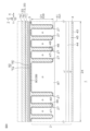
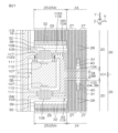
- FIG. 1 is a schematic plan view of a semiconductor device according to an embodiment of the present disclosure.
- FIG. 2 is a schematic plan view for explaining the internal structure of the semiconductor device.
- FIG. 3 is an enlarged view of the portion enclosed by III in FIG.
- FIG. 4 is a cross-sectional view taken along line IV-IV in FIG.
- FIG. 5 is a cross-sectional view taken along line VV in FIG.
- FIG. 6 is a cross-sectional view taken along line VI-VI in FIG.
- FIG. 7 is a cross-sectional view taken along line VII-VII in FIG.
- FIG. 8 is a cross-sectional view taken along line VIII-VIII in FIG.
- FIG. 9 is a cross-sectional view taken along line IX-IX in FIG.
- FIG. 1 is a schematic plan view of a semiconductor device according to an embodiment of the present disclosure.
- FIG. 2 is a schematic plan view for explaining the internal structure of the semiconductor device.
- FIG. 3 is an enlarged view
- FIG. 10 is a cross-sectional view taken along line XX in FIG.
- FIG. 11 is a cross-sectional view taken along line XI-XI of FIG.
- FIG. 12 is an enlarged view of the portion surrounded by XII in FIG.
- FIG. 13 is a cross-sectional view taken along line XIII-XIII in FIG.
- FIG. 14 is a diagram showing a modification of the gate-assist trench structure of FIG.
- FIG. 15 is a diagram showing a modification of the gate-assist trench structure of FIG.
- FIG. 16 is a diagram showing a modification of the gate-assist trench structure of FIG.
- FIG. 17 is an enlarged view of the portion surrounded by XVII in FIG. FIG.
- FIG. 18 is a cross-sectional view taken along line XVIII-XVIII in FIG.
- FIG. 19 is a cross-sectional view taken along line XIX-XIX in FIG.
- FIG. 20 is a diagram showing a modified example of the arrangement pattern of the IGBT regions and the diode regions.
- FIG. 21 is an enlarged view of the portion surrounded by XXI in FIG.
- FIG. 1 is a schematic plan view of a semiconductor device 1 according to one embodiment of the present disclosure.
- the semiconductor device 1 is an electronic component having an RC-IGBT (Reverse Conducting-Insulated Gate Bipolar Transistor) that has an IGBT and a diode integrated together.
- the semiconductor device 1 includes a semiconductor chip 2 having a rectangular parallelepiped shape.
- the semiconductor chip 2 has a first main surface 3 on one side, a second main surface 4 on the other side, and side surfaces 5A, 5B, 5C, and 5D that connect the first main surface 3 and the second main surface 4.
- the first main surface 3 and the second main surface 4 are formed in a quadrangular shape in a plan view (hereinafter simply referred to as "plan view") seen from their normal direction Z.
- the first main surface 3 and the second main surface 4 may be referred to as the front and back surfaces of the semiconductor chip 2, respectively.
- the side surface 5A and the side surface 5C extend along the first direction X and face each other in a second direction Y that intersects the first direction X.
- the side surface 5B and the side surface 5D extend along the second direction Y and face each other in the first direction X.
- the second direction Y is specifically perpendicular to the first direction X.
- the electrode film 6 is formed on the first main surface 3.
- the electrode film 6 includes a plurality of terminal electrodes 7-12 and a plurality of wirings 13-15.
- the multiple terminal electrodes 7-11 are arranged at intervals along the side surface of the semiconductor chip 2.
- the multiple terminal electrodes 7-11 are concentrated on one side surface of the semiconductor chip 2 (side surface 5B in FIG. 1) and aligned in a row along side surface 5B.
- the electrode film 6 includes a gate terminal electrode 7 and a gate wiring 13 as components related to the gate of the RC-IGBT.
- the gate wiring 13 transmits the gate signal applied to the gate terminal electrode 7 to the gate of the IGBT.
- the gate terminal electrode 7 is disposed at the center of the multiple terminal electrodes 7-11.
- the gate wiring 13 integrally includes an annular first portion 16 drawn from the gate terminal electrode 7 along the side surfaces 5A-5D of the semiconductor chip 2, and a second portion 17 that crosses the active region 18 surrounded by the first portion 16.
- the gate wiring 13 may be referred to as a gate finger.
- the first portion 16 and the second portion 17 of the gate wiring 13 may be referred to as an outer gate finger and an inner gate finger, respectively.
- the first portion 16 and the second portion 17 of the gate wiring 13 may be referred to as an outer extension electrode and an inner extension electrode, respectively.
- the active region 18 is the region in which the RC-IGBT is formed.
- the region outside the active region 18 is the peripheral region 19.
- the peripheral region 19 extends in a band shape along the periphery of the active region 18. Specifically, the peripheral region 19 is set to be endless (square ring shape) surrounding the active region 18 in a plan view.
- the active region 18 is divided into a number of partitioned regions 20 by the second portion 17 of the gate wiring 13.
- Each of the partitioned regions 20 has a rectangular shape extending along the first direction X.
- the partitioned regions 20 are adjacent to each other with the second portion 17 of the gate wiring 13 therebetween.
- the second portions 17 of the gate wirings 13 cross the active region 18.
- the second portions 17 are arranged at intervals in the second direction Y and are formed in stripes extending in the first direction X.
- One end and the other end of each second portion 17 are connected to different positions in the first portion 16.
- the base end (which may be called the terminal end or pad end) of each second portion 17 on the side of the terminal electrodes 7-11 is connected to the first portion 16, and the opposite end is not connected to the first portion 16 and may be used as a termination portion.
- the second portions 17 include a central wiring 21 extending from near the gate terminal electrode 7, and a plurality of side wirings 22 extending from positions away from the gate terminal electrode 7 in the second direction Y.
- a central wiring 21 extending from near the gate terminal electrode 7, and a plurality of side wirings 22 extending from positions away from the gate terminal electrode 7 in the second direction Y.
- one central wiring 21 and two side wirings 22 are provided on each side of the central wiring 21 in the second direction Y. This divides the active region 18 into six partitioned regions 20.
- the electrode film 6 includes an emitter terminal electrode 12 as a component related to the emitter of the RC-IGBT.
- the emitter terminal electrode 12 is disposed in each partition region 20.
- one emitter terminal electrode 12 is provided in each partition region 20.
- a number of emitter terminal electrodes 12 are provided, the same number as the number of partition regions 20.
- a number of emitter terminal electrodes 12 that are physically separated from one another may be provided in each partition region 20.
- the electrode film 6 further includes a first sense terminal electrode 8, a second sense terminal electrode 9, a current detection terminal electrode 10, and an open terminal electrode 11.
- the first sense terminal electrode 8 and the second sense terminal electrode 9 transmit control signals that control a sensor region 23 (temperature sensor) located in the center of the active region 18.
- the current detection terminal electrode 10 is an electrode for detecting the current flowing through the active region 18 and extracting it to the outside.
- the open terminal electrode 11 is in an electrically floating state.
- the electrode film 6 includes a first sense wiring 14 and a second sense wiring 15.
- the first sense wiring 14 is electrically connected to the first sense terminal electrode 8.
- the first sense wiring 14 extends from the outer periphery region 19 toward the sensor region 23.
- the first sense wiring 14 transmits a control signal for the temperature sensor.
- the second sense wiring 15 is electrically connected to the second sense terminal electrode 9.
- the second sense wiring 15 extends from the outer periphery region 19 toward the sensor region 23.
- the second sense wiring 15 transmits a control signal for the temperature sensor.
- the gate wiring 13 (central wiring 21), the first sense wiring 14, and the second sense wiring 15 run parallel to each other with a gap therebetween in the first direction X.
- FIG. 2 is a schematic plan view for explaining the internal structure of the semiconductor device 1. For clarity, FIG. 2 shows the terminal electrodes 7 to 11 and the gate wiring 13 of the electrode film 6, and omits other parts of the electrode film 6.
- the active region 18 includes an IGBT region 24 and a diode region 25.
- the IGBT region 24 is shown hatched for clarity.
- the IGBT region 24 is the region in which an IGBT is formed.
- the diode region 25 is the region in which a diode is formed.
- the diode region 25 is adjacent to the IGBT region 24.
- the active region 18 specifically includes an RC-IGBT array 26.
- a plurality of RC-IGBT arrays 26 (six in this embodiment) are formed at intervals in the second direction Y. Adjacent RC-IGBT arrays 26 are separated by gate wiring 13.
- the RC-IGBT array 26 has a first end on one side (side surface 5B side) and a second end on the other side (side surface 5D side).
- the first end of the RC-IGBT array 26 may be referred to as a terminal side end or a pad side end.
- the second end of the RC-IGBT array 26 may be referred to as a termination side end.
- the RC-IGBT array 26 has a loop arrangement including a repeating diode region 25, an IGBT region 24, a diode region 25, an IGBT region 24, a diode region 25, etc., arranged in a row from a first end to a second end along a first direction X.
- the first end of the RC-IGBT array 26 is formed by the diode region 25.
- the second end of the RC-IGBT array 26 is formed by the diode region 25.
- the first end of the RC-IGBT array 26 may be formed by the IGBT region 24.
- the second end of the RC-IGBT array 26 may be formed by the IGBT region 24.
- a plurality of IGBT regions 24 are dispersed and arranged in the active region 18.
- the plurality of IGBT regions 24 are formed at intervals along the first direction X and the second direction Y.
- the plurality of IGBT regions 24 are arranged in a matrix in a plan view.
- the plurality of IGBT regions 24 face each other along the first direction X and face each other along the second direction Y.
- each of the IGBT regions 24 is formed in a quadrangular shape in a plan view. More specifically, each of the IGBT regions 24 is formed in a rectangular shape extending along the second direction Y.
- the width WI in the first direction X of each IGBT region 24 may be 10 ⁇ m or more and 1000 ⁇ m or less.
- the width WI may be 10 ⁇ m or more and 100 ⁇ m or less, 100 ⁇ m or more and 200 ⁇ m or less, 200 ⁇ m or more and 300 ⁇ m or less, 300 ⁇ m or more and 400 ⁇ m or less, 400 ⁇ m or more and 500 ⁇ m or less, 500 ⁇ m or more and 600 ⁇ m or less, 600 ⁇ m or more and 700 ⁇ m or less, 700 ⁇ m or more and 800 ⁇ m or less, 800 ⁇ m or more and 900 ⁇ m or less, or 900 ⁇ m or more and 1000 ⁇ m or less. It is preferable that the width WI is 100 ⁇ m or more. It is even more preferable that the width WI is 200 ⁇ m or more.
- a plurality of diode regions 25 are distributed and arranged in the active region 18.
- the plurality of diode regions 25 are formed at intervals along the first direction X and the second direction Y.
- the plurality of diode regions 25 are arranged in a matrix in a planar view.
- the plurality of diode regions 25 face each other along the first direction X and face each other along the second direction Y.
- each of the multiple diode regions 25 is formed adjacent to the IGBT region 24 in the first direction X.
- each of the multiple diode regions 25 is formed in a quadrangular shape in a plan view.
- each of the multiple diode regions 25 is formed in a rectangular shape extending along the second direction Y.
- each diode region 25 is preferably equal to or less than the planar area of each IGBT region 24. It is even more preferable that the planar area of each diode region 25 is less than the planar area of each IGBT region 24. It is preferable that the width WD of each diode region 25 in the first direction X is equal to or less than the width WI of each IGBT region 24. It is even more preferable that the width WD of each diode region 25 is less than the width WI of each IGBT region 24.
- the width WD may be 5 ⁇ m or more and less than 1000 ⁇ m.
- the width WD may be 5 ⁇ m or more and less than 100 ⁇ m, 100 ⁇ m or more and less than 200 ⁇ m, 200 ⁇ m or more and less than 300 ⁇ m, 300 ⁇ m or more and less than 400 ⁇ m, 400 ⁇ m or more and less than 500 ⁇ m, 500 ⁇ m or more and less than 600 ⁇ m, 600 ⁇ m or more and less than 700 ⁇ m, 700 ⁇ m or more and less than 800 ⁇ m, 800 ⁇ m or more and less than 900 ⁇ m, or 900 ⁇ m or more and less than 1000 ⁇ m.
- the width WD is preferably 100 ⁇ m or more. It is even more preferable that the width WD is 200 ⁇ m or more.
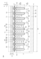
- FIG. 3 is an enlarged view of the portion surrounded by III in FIG. 2, showing a portion of the multiple IGBT regions 24 and multiple diode regions 25.
- the planar structure of the IGBT regions 24 and diode regions 25 described below may be applied to all the IGBT regions 24 and all the diode regions 25 of the semiconductor chip 2, or may be selectively applied to some of the IGBT regions 24 and diode regions 25.
- the planar structure described below is a structure that can be applied to at least one IGBT region 24 and diode region 25.
- multiple types of trench electrode structures 27-29 are formed in a striped pattern on the first main surface 3 of the semiconductor chip 2.
- the multiple trench electrode structures 27-29 extend parallel to each other along the second direction Y.
- the multiple trench electrode structures 27-29 are a trench gate structure 27, an emitter trench structure 28, and a diode side trench structure 29.
- the trench gate structure 27, the emitter trench structure 28, and the diode side trench structure 29 are indicated by hatching.
- the multiple trench gate structures 27 are formed in the IGBT region 24.
- the trench gate structures 27 are formed in a band shape extending along the second direction Y in a plan view.
- the multiple trench gate structures 27 are formed in a stripe shape as a whole.
- the multiple trench gate structures 27 cross from one side to the other side in the second direction Y directly below the gate wiring 13. This allows the trench gate structure 27 to span a plurality of partition regions 20.
- the trench gate structure 27 has an end portion 30 on each of the one side and the other side in the second direction Y. In FIG. 3, the end portion 30 on one side is shown.
- the termination portions 30 of the trench gate structures 27 are formed for each pair of trench gate structures 27.
- the termination portions 30 connect adjacent trench gate structures 27 at the outer peripheral region 19.
- the termination portions 30 are formed in a round shape in a plan view.
- the multiple emitter trench structures 28 are formed in the IGBT region 24.
- the emitter trench structures 28 are formed in a band shape extending along the second direction Y in a plan view.
- the multiple emitter trench structures 28 extend parallel to the trench gate structures 27, and the emitter trench structures 28 and the trench gate structures 27 as a whole are formed in a stripe shape.
- the multiple emitter trench structures 28 are sandwiched between the multiple trench gate structures 27 in the first direction X. In this form, a pair of emitter trench structures 28 are sandwiched between the multiple trench gate structures 27 in the first direction X.
- the multiple emitter trench structures 28 do not cross the gate wiring 13, and have terminal portions 31 inside the IGBT region 24 away from the gate wiring 13 in the second direction Y.
- the terminal portions 31 of the emitter trench structures 28 are formed one for each pair of emitter trench structures 28.
- the terminal portions 31 connect adjacent emitter trench structures 28 within the IGBT region 24.
- the terminal portions 31 are formed in a round shape in a plan view.
- the multiple diode-side trench structures 29 are formed in the diode region 25.
- the diode-side trench structures 29 are formed in a band shape extending along the second direction Y in a plan view.
- the multiple diode-side trench structures 29 are formed in a stripe shape as a whole.
- the multiple diode-side trench structures 29 cross from one side to the other side in the second direction Y directly below the gate wiring 13. This allows the common diode-side trench structure 29 to span the multiple partition regions 20.
- the diode-side trench structure 29 has an end portion 32 on each of the one side and the other side in the second direction Y. In FIG. 3, the end portion 32 on one side is shown.
- the termination portions 32 of the diode side trench structures 29 are formed for each pair of diode side trench structures 29.
- the termination portions 32 connect adjacent diode side trench structures 29 at the outer peripheral region 19.
- the termination portions 32 are formed in a round shape in a plan view.
- the gate wiring 13 is an electrode that extends across the multiple trench gate structures 27 in the first direction X.
- the gate wiring 13 may also be referred to as a gate extension electrode 33.
- the gate extension electrode 33 includes a first electrode layer 34 and a second electrode layer 35.
- the second electrode layer 35 is a layer laminated on the first electrode layer 34.
- the second electrode layer 35 is an electrode layer that appears on the outermost surface of the gate extension electrode 33, and may be referred to as a surface layer.
- the second electrode layer 35 is a layer with a lower resistance than the first electrode layer 34.
- the contour of the second electrode layer 35 coincides with the contour of the gate extension electrode 33.
- the second electrode layer 35 is formed in a strip shape that continuously extends across the multiple IGBT regions 24 and multiple diode regions 25 that are alternately arranged.
- the second electrode layer 35 is strip-shaped with a constant width in the second direction Y.
- the first electrode layer 34 is formed avoiding the region directly above the diode-side trench structure 29. Specifically, the first electrode layer 34 is selectively divided by the non-contact section 36 where the second electrode layer 35 and the diode region 25 face each other. As a result, the first electrode layer 34 is selectively disposed in the contact section 37 where the second electrode layer 35 and the IGBT region 24 face each other. In other words, the gate extension electrode 33 does not have the first electrode layer 34 directly above the trench gate structure 27, and selectively has the second electrode layer 35.
- the first electrode layer 34 is formed in a long strip shape in the first direction X, and collectively covers the multiple trench gate structures 27.
- the first electrode layer 34 is a layer electrically connected to the multiple trench gate structures 27, and may be referred to as a first contact layer 38.
- a second contact layer 39 is formed on the first main surface 3 of the semiconductor chip 2.
- the second contact layer 39 is a layer that is electrically connected to the multiple diode-side trench structures 29.
- the second contact layer 39 is formed in a long strip shape in the first direction X, and collectively covers the multiple diode-side trench structures 29. In this form, the second contact layer 39 is separated from the gate extension electrode 33 toward the inside of the diode region 25 and extends parallel to the gate extension electrode 33.
- a third contact layer 40 is formed on the first main surface 3 of the semiconductor chip 2.
- the third contact layer 40 is a layer that is electrically connected to the multiple emitter trench structures 28.
- the third contact layer 40 is formed in an island shape in a plan view, and collectively covers the terminal ends 31 of a pair of emitter trench structures 28.
- FIG. 4 is a cross-sectional view taken along line IV-IV in FIG. 3.
- FIG. 5 is a cross-sectional view taken along line V-V in FIG. 3.
- the basic cross-sectional structures of the IGBT region 24 and the diode region 25 will be described with reference to FIG. 4 and FIG. 5.
- the semiconductor device 1 includes an n - type drift region 41 formed inside the semiconductor chip 2. Specifically, the drift region 41 is formed over the entire area of the semiconductor chip 2 in the first direction X and the second direction Y. The drift region 41 is formed in a surface layer portion of the first main surface 3 of the semiconductor chip 2 in the normal direction Z (thickness direction of the semiconductor chip 2). The n-type impurity concentration of the drift region 41 may be 1.0 ⁇ 10 13 cm -3 or more and 1.0 ⁇ 10 15 cm -3 or less.
- the semiconductor chip 2 has a single-layer structure including an n - type semiconductor substrate 42.
- the semiconductor substrate 42 may be a silicon FZ (Floating Zone) substrate formed through an FZ method.
- the drift region 41 is formed by the semiconductor substrate 42.
- the semiconductor device 1 includes a collector terminal electrode 43 formed on the second main surface 4 of the semiconductor chip 2.
- the collector terminal electrode 43 is electrically connected to the second main surface 4. Specifically, the collector terminal electrode 43 is electrically connected to the IGBT region 24 (collector region 45 described later) and the diode region 25 (cathode region 58 described later).
- the collector terminal electrode 43 forms an ohmic contact with the second main surface 4.
- the collector terminal electrode 43 transmits a collector signal to the IGBT region 24 and the diode region 25.
- the collector terminal electrode 43 may include at least one of a Ti layer, a Ni layer, an Au layer, an Ag layer, and an Al layer.
- the collector terminal electrode 43 may have a single layer structure including a Ti layer, a Ni layer, an Au layer, an Ag layer, or an Al layer.
- the collector terminal electrode 43 may have a laminated structure in which at least two of a Ti layer, a Ni layer, an Au layer, an Ag layer, and an Al layer are laminated in any manner.
- the semiconductor device 1 includes an n-type buffer layer 44 formed in a surface layer portion of the second main surface 4 of the semiconductor chip 2.
- the buffer layer 44 may be formed over the entire surface layer portion of the second main surface 4.
- the n-type impurity concentration of the buffer layer 44 is higher than the n-type impurity concentration of the drift region 41.
- the n-type impurity concentration of the buffer layer 44 may be 1.0 ⁇ 10 15 cm -3 or more and 1.0 ⁇ 10 17 cm -3 or less.
- the thickness of the buffer layer 44 may be 0.5 ⁇ m or more and 30 ⁇ m or less.
- the thickness of the buffer layer 44 may be 0.5 ⁇ m or more and 5 ⁇ m or less, 5 ⁇ m or more and 10 ⁇ m or less, 10 ⁇ m or more and 15 ⁇ m or less, 15 ⁇ m or more and 20 ⁇ m or less, 20 ⁇ m or more and 25 ⁇ m or less, or 25 ⁇ m or more and 30 ⁇ m or less.
- Each IGBT region 24 includes a p-type collector region 45 formed in a surface layer portion of the second main surface 4 of the semiconductor chip 2.
- the collector region 45 is exposed from the second main surface 4.
- the collector region 45 may be formed throughout the entire IGBT region 24 in the surface layer portion of the second main surface 4.
- the p-type impurity concentration of the collector region 45 may be not less than 1.0 ⁇ 10 15 cm -3 and not more than 1.0 ⁇ 10 18 cm -3 .
- the collector region 45 forms an ohmic contact with the collector terminal electrode 43.
- Each IGBT region 24 includes a FET structure 46 formed on the first main surface 3 of the semiconductor chip 2.
- each IGBT region 24 includes a trench-gate type FET structure 46.
- the FET structure 46 includes a trench gate structure 27 formed on the first main surface 3.
- the trench gate structures 27 are formed in the IGBT region 24 at intervals along the first direction X.
- the distance between two adjacent trench gate structures 27 in the first direction X may be 1 ⁇ m or more and 8 ⁇ m or less.
- the distance between two trench gate structures 27 may be 1 ⁇ m or more and 2 ⁇ m or less, 2 ⁇ m or more and 3 ⁇ m or less, 3 ⁇ m or more and 4 ⁇ m or less, 4 ⁇ m or more and 5 ⁇ m or less, 5 ⁇ m or more and 6 ⁇ m or less, 6 ⁇ m or more and 7 ⁇ m or less, or 7 ⁇ m or more and 8 ⁇ m or less.
- Each trench gate structure 27 includes a gate trench 47, a gate insulating layer 48, and a gate electrode layer 49.
- the gate trench 47 is formed in the first major surface 3.
- the gate trench 47 includes a sidewall and a bottom wall. The sidewall of the gate trench 47 may be formed perpendicular to the first major surface 3.
- the sidewalls of the gate trench 47 may slope downward from the first main surface 3 toward the bottom wall.
- the gate trench 47 may be formed in a tapered shape in which the opening area on the opening side is larger than the bottom area.
- the bottom wall of the gate trench 47 may be formed parallel to the first main surface 3.
- the bottom wall of the gate trench 47 may be formed in a curved shape toward the second main surface 4.
- the gate trench 47 includes a bottom wall edge portion.
- the bottom wall edge portion connects the sidewalls and bottom wall of the gate trench 47.
- the bottom wall edge portion may be formed in a curved shape toward the second main surface 4.
- the depth D1 of the gate trench 47 may be 2 ⁇ m or more and 10 ⁇ m or less.
- the depth D1 of the gate trench 47 may be 2 ⁇ m or more and 3 ⁇ m or less, 3 ⁇ m or more and 4 ⁇ m or less, 4 ⁇ m or more and 5 ⁇ m or less, 5 ⁇ m or more and 6 ⁇ m or less, 6 ⁇ m or more and 7 ⁇ m or less, 8 ⁇ m or more and 9 ⁇ m or less, or 9 ⁇ m or more and 10 ⁇ m or less.
- the depth D1 of the gate trench 47 may be defined as the distance between the deepest depth position of the bottom wall of the gate trench 47 and the first main surface 3.
- the width of the gate trench 47 may be 0.5 ⁇ m or more and 3 ⁇ m or less.
- the width of the gate trench 47 is the width of the gate trench 47 in the first direction X.
- the width of the gate trench 47 may be 0.5 ⁇ m or more and 1 ⁇ m or less, 1 ⁇ m or more and 1.5 ⁇ m or less, 1.5 ⁇ m or more and 2 ⁇ m or less, 2 ⁇ m or more and 2.5 ⁇ m or less, or 2.5 ⁇ m or more and 3 ⁇ m or less.
- the gate insulating layer 48 is formed in the form of a film along the inner wall of the gate trench 47.
- the gate insulating layer 48 defines a recess space within the gate trench 47.
- the gate insulating layer 48 includes a silicon oxide film.
- the gate insulating layer 48 may include a silicon nitride film instead of or in addition to the silicon oxide film.
- the gate electrode layer 49 is embedded in the gate trench 47 with the gate insulating layer 48 sandwiched therebetween. Specifically, the gate electrode layer 49 is embedded in a recess space defined by the gate insulating layer 48 in the gate trench 47.
- the gate electrode layer 49 is controlled by a gate signal.
- the gate electrode layer 49 may include conductive polysilicon.
- the FET structure 46 includes a p-type body region 50 formed in a surface layer portion of the first main surface 3 of the semiconductor chip 2.
- the p-type impurity concentration of the body region 50 may be 1.0 ⁇ 10 17 cm ⁇ 3 or more and 1.0 ⁇ 10 18 cm ⁇ 3 or less.
- the body region 50 is formed on both sides of the trench gate structure 27.
- the body region 50 is formed in a strip shape extending along the trench gate structure 27 in a plan view.
- the body region 50 is exposed from the side wall of the gate trench 47.
- the bottom of the body region 50 is formed in a region between the first main surface 3 and the bottom wall of the gate trench 47 with respect to the normal direction Z.
- the FET structure 46 includes an n + type emitter region 51 formed in a surface layer portion of the body region 50.
- the n-type impurity concentration of the emitter region 51 is higher than the n-type impurity concentration of the drift region 41.
- the n-type impurity concentration of the emitter region 51 may be 1.0 ⁇ 10 19 cm ⁇ 3 or more and 1.0 ⁇ 10 20 cm ⁇ 3 or less.
- the FET structure 46 includes a plurality of emitter regions 51 formed on both sides of the trench gate structure 27.
- the emitter regions 51 are formed in a strip shape extending along the trench gate structure 27 in a plan view.
- the emitter regions 51 are exposed from the first main surface 3 and the sidewalls of the gate trench 47.
- the bottoms of the emitter regions 51 are formed in a region between the upper end of the gate electrode layer 49 and the bottom of the body region 50 in the normal direction Z.
- the FET structure 46 includes an n + type carrier storage region 52 formed in a region on the second main surface 4 side of the body region 50 in the semiconductor chip 2.
- the n type impurity concentration of the carrier storage region 52 is higher than the n type impurity concentration of the drift region 41.
- the n type impurity concentration of the carrier storage region 52 may be 1.0 ⁇ 10 15 cm -3 or more and 1.0 ⁇ 10 17 cm -3 or less.
- the FET structure 46 includes a plurality of carrier storage regions 52 formed on both sides of the trench gate structure 27.
- the carrier storage regions 52 are formed in a strip shape extending along the trench gate structure 27 in a plan view.
- the carrier storage regions 52 are exposed from the side walls of the gate trench 47.
- the bottoms of the carrier storage regions 52 are formed in the region between the bottom of the body region 50 and the bottom wall of the gate trench 47 in the normal direction Z.
- the carrier storage region 52 prevents carriers (holes) supplied to the semiconductor chip 2 from being drawn back (discharged) to the body region 50. This causes holes to accumulate in the region directly below the FET structure 46 in the semiconductor chip 2. As a result, the on-resistance and on-voltage are reduced.
- the FET structure 46 includes a contact trench 53 formed in the first main surface 3 of the semiconductor chip 2.
- the FET structure 46 includes a plurality of contact trenches 53 formed on both sides of the trench gate structure 27.
- the contact trenches 53 expose the emitter region 51.
- the contact trenches 53 penetrate the emitter region 51.
- the contact trench 53 is formed at a distance from the trench gate structure 27 in the first direction X.
- the contact trench 53 extends in a band shape along the trench gate structure 27 in a plan view.
- the FET structure 46 includes a p + type contact region 54 formed in a region along the bottom wall of the contact trench 53 in the body region 50.
- the p-type impurity concentration of the contact region 54 is higher than the p-type impurity concentration of the body region 50.
- the p-type impurity concentration of the contact region 54 may be not less than 1.0 ⁇ 10 19 cm ⁇ 3 and not more than 1.0 ⁇ 10 20 cm ⁇ 3 .
- the contact region 54 is exposed from the bottom wall of the contact trench 53. In a plan view, the contact region 54 extends in a band shape along the contact trench 53. The bottom of the contact region 54 is formed in the region between the bottom wall of the contact trench 53 and the bottom of the body region 50 in the normal direction Z.
- the gate electrode layer 49 faces the body region 50 and the emitter region 51 with the gate insulating layer 48 in between. In this configuration, the gate electrode layer 49 also faces the carrier storage region 52 with the gate insulating layer 48 in between.
- the channel of the IGBT is formed in the region between the emitter region 51 and the drift region 41 (carrier storage region 52) in the body region 50. The on/off of the channel is controlled by a gate signal.
- Each IGBT region 24 includes an emitter trench structure 28 on the first main surface 3 of the semiconductor chip 2. Specifically, each IGBT region 24 includes a plurality of emitter trench structures 28 formed on both sides of the FET structure 46. The emitter trench structures 28 are formed in regions adjacent to the FET structure 46 in the surface layer portion of the first main surface 3. The emitter trench structures 28 are formed in a band shape extending along the second direction Y in a plan view. The emitter trench structures 28 may be band-shaped parallel to the trench gate structure 27.
- the emitter trench structure 28 includes an emitter trench 55, an emitter insulating layer 56, and an emitter potential electrode layer 57.
- the emitter trench 55 is formed in the first main surface 3 of the semiconductor chip 2.
- the emitter trench 55 includes a sidewall and a bottom wall. The sidewall of the emitter trench 55 may be formed perpendicular to the first main surface 3.
- the sidewall of the emitter trench 55 may be inclined downward from the first main surface 3 toward the bottom wall.
- the emitter trench 55 may be formed in a tapered shape in which the opening area on the opening side is larger than the bottom area.
- the emitter region 51, the body region 50, and the carrier storage region 52 are exposed from the sidewall (outer sidewall) of the emitter trench 55 facing the FET structure 46.
- the bottom wall of the emitter trench 55 may be formed parallel to the first main surface 3.
- the bottom wall of the emitter trench 55 may be formed in a curved shape toward the second main surface 4.
- the emitter trench 55 includes a bottom wall edge portion.
- the bottom wall edge portion connects the sidewall and the bottom wall of the emitter trench 55.
- the bottom wall edge portion may be formed in a curved shape toward the second main surface 4 of the semiconductor chip 2.
- the depth D3 of the emitter trench 55 may be 2 ⁇ m or more and 10 ⁇ m or less.
- the depth D3 of the emitter trench 55 may be 2 ⁇ m or more and 3 ⁇ m or less, 3 ⁇ m or more and 4 ⁇ m or less, 4 ⁇ m or more and 5 ⁇ m or less, 5 ⁇ m or more and 6 ⁇ m or less, 6 ⁇ m or more and 7 ⁇ m or less, 8 ⁇ m or more and 9 ⁇ m or less, or 9 ⁇ m or more and 10 ⁇ m or less.
- the depth D3 of the emitter trench 55 may be equal to the depth D1 of the gate trench 47.
- the width of the emitter trench 55 may be 0.5 ⁇ m or more and 3 ⁇ m or less.
- the width of the emitter trench 55 is the width of the emitter trench 55 in the first direction X.
- the width of the emitter trench 55 may be 0.5 ⁇ m or more and 1 ⁇ m or less, 1 ⁇ m or more and 1.5 ⁇ m or less, 1.5 ⁇ m or more and 2 ⁇ m or less, 2 ⁇ m or more and 2.5 ⁇ m or less, or 2.5 ⁇ m or more and 3 ⁇ m or less.
- the width of the emitter trench 55 may be equal to the width of the gate trench 47.
- the emitter insulating layer 56 is formed in the form of a film along the inner wall of the emitter trench 55.
- the emitter insulating layer 56 defines a recess space within the emitter trench 55.
- the emitter insulating layer 56 includes a silicon oxide film.
- the emitter insulating layer 56 may include a silicon nitride film instead of or in addition to the silicon oxide film.
- the emitter potential electrode layer 57 is embedded in the emitter trench 55 with the emitter insulating layer 56 sandwiched therebetween. Specifically, the emitter potential electrode layer 57 is embedded in a recess space defined by the emitter insulating layer 56 in the emitter trench 55.
- the emitter potential electrode layer 57 may include conductive polysilicon.
- the emitter potential electrode layer 57 is controlled by an emitter signal.
- each diode region 25 includes an n + type cathode region 58 (second impurity region) formed in a surface layer portion of the second main surface 4 of the semiconductor chip 2.
- the n type impurity concentration of the cathode region 58 is higher than the n type impurity concentration of the drift region 41.
- the n type impurity concentration of the cathode region 58 may be 1.0 ⁇ 10 19 cm ⁇ 3 or more and 1.0 ⁇ 10 20 cm ⁇ 3 or less.
- the cathode region 58 is exposed from the second main surface 4.
- the cathode region 58 forms an ohmic contact with the collector terminal electrode 43.
- Each diode region 25 includes a cell isolation structure 60 that defines a diode cell region 59. Specifically, each diode region 25 includes a plurality of cell isolation structures 60 that define a plurality of diode cell regions 59. The cell isolation structure 60 corresponds to the diode-side trench structure 29 in FIG. 3.
- the cell separation structure 60 includes a cell separation trench 61, a cell separation insulating layer 62, and a cell separation electrode layer 63.
- the cell separation trench 61 is formed on the first main surface 3.
- the cell separation trench 61 includes a sidewall and a bottom wall. The sidewall of the cell separation trench 61 may be formed perpendicular to the first main surface 3.
- the sidewalls of the cell separation trench 61 may slope downward from the first main surface 3 toward the bottom wall.
- the cell separation trench 61 may be formed in a tapered shape in which the opening area on the opening side is larger than the bottom area.
- the bottom wall of the cell separation trench 61 may be formed parallel to the first main surface 3.
- the bottom wall of the cell separation trench 61 may be formed in a curved shape toward the second main surface 4.
- the cell separation trench 61 includes a bottom wall edge portion.
- the bottom wall edge portion connects the sidewalls and the bottom wall of the cell separation trench 61.
- the bottom wall edge portion may be formed in a curved shape toward the second main surface 4.
- the depth D2 of the cell isolation trench 61 may be 2 ⁇ m or more and 10 ⁇ m or less.
- the depth D2 of the cell isolation trench 61 may be 2 ⁇ m or more and 3 ⁇ m or less, 3 ⁇ m or more and 4 ⁇ m or less, 4 ⁇ m or more and 5 ⁇ m or less, 5 ⁇ m or more and 6 ⁇ m or less, 6 ⁇ m or more and 7 ⁇ m or less, 8 ⁇ m or more and 9 ⁇ m or less, or 9 ⁇ m or more and 10 ⁇ m or less.
- the depth D2 of the cell isolation trench 61 may be equal to the depth D1 of the gate trench 47.
- the depth D2 of the cell isolation trench 61 may be defined as the distance between the deepest depth position of the bottom wall of the cell isolation trench 61 and the first main surface 3.
- the width of the cell isolation trench 61 may be 0.5 ⁇ m or more and 3 ⁇ m or less.
- the width of the cell isolation trench 61 is the width of the cell isolation trench 61 in the first direction X.
- the width of the cell isolation trench 61 may be 0.5 ⁇ m or more and 1 ⁇ m or less, 1 ⁇ m or more and 1.5 ⁇ m or less, 1.5 ⁇ m or more and 2 ⁇ m or less, 2 ⁇ m or more and 2.5 ⁇ m or less, or 2.5 ⁇ m or more and 3 ⁇ m or less.
- the width of the cell isolation trench 61 may be equal to the width of the gate trench 47.
- the cell isolation insulating layer 62 is formed in the form of a film along the inner wall of the cell isolation trench 61.
- the cell isolation insulating layer 62 defines a recess space within the cell isolation trench 61.
- the cell isolation insulating layer 62 includes a silicon oxide film.
- the cell isolation insulating layer 62 may include a silicon nitride film instead of or in addition to the silicon oxide film.
- the cell separation electrode layer 63 is embedded in the cell separation trench 61 with the cell separation insulating layer 62 sandwiched therebetween. Specifically, the cell separation electrode layer 63 is embedded in a recess space defined by the cell separation insulating layer 62 in the cell separation trench 61.
- the cell separation electrode layer 63 is controlled by an emitter signal.
- the cell separation electrode layer 63 may include conductive polysilicon.
- Each diode region 25 includes ap ⁇ type anode region 64 (first impurity region) formed in a surface layer portion of the first main surface 3 of the semiconductor chip 2.
- the p-type impurity concentration of the anode region 64 may be equal to or lower than the p-type impurity concentration of the body region 50.
- the p-type impurity concentration of the anode region 64 is preferably lower than the p-type impurity concentration of the body region 50.
- the p-type impurity concentration of the anode region 64 may be equal to or higher than 1.0 ⁇ 10 15 cm ⁇ 3 and lower than 1.0 ⁇ 10 18 cm ⁇ 3 .
- An anode region 64 is formed in each diode cell region 59. Therefore, a plurality of anode regions 64 are arranged at equal intervals in the first direction X, and are formed in a stripe shape overall.
- the anode region 64 forms a pn junction 65 with the semiconductor chip 2. This forms a pn junction diode D with the anode region 64 as the anode and the semiconductor chip 2 (cathode region 58) as the cathode.
- the anode region 64 includes a diode trench 66 formed in the first main surface 3 of the semiconductor chip 2.
- the anode region 64 includes a plurality of diode trenches 66 formed on both sides of the cell isolation structure 60.
- the diode trenches 66 expose the anode region 64.
- the diode trenches 66 are formed at intervals in the first direction X from the cell isolation structure 60.
- the diode trenches 66 extend in a band shape along the cell isolation structure 60 in a plan view.
- the semiconductor device 1 includes an interlayer insulating layer 67 formed on the first main surface 3 of the semiconductor chip 2.
- the interlayer insulating layer 67 is formed in a film shape along the first main surface 3, and selectively covers the first main surface 3. Specifically, the interlayer insulating layer 67 selectively covers the IGBT region 24 and the diode region 25.
- the interlayer insulating layer 67 may contain silicon oxide or silicon nitride.
- the interlayer insulating layer 67 may contain at least one of NSG (Non-doped Silicate Glass), PSG (Phosphor Silicate Glass), and BPSG (Boron Phosphor Silicate Glass).
- the thickness of the interlayer insulating layer 67 may be 0.1 ⁇ m or more and 1 ⁇ m or less.
- the thickness of the interlayer insulating layer 67 may be 0.1 ⁇ m or more and 0.2 ⁇ m or less, 0.2 ⁇ m or more and 0.4 ⁇ m or less, 0.4 ⁇ m or more and 0.6 ⁇ m or less, 0.6 ⁇ m or more and 0.8 ⁇ m or less, or 0.8 ⁇ m or more and 1 ⁇ m or less.
- the interlayer insulating layer 67 has a laminated structure including a first insulating layer 68, a second insulating layer 69, and a third insulating layer 70, which are laminated in this order from the first main surface 3 side.
- the first insulating layer 68 preferably includes silicon oxide (e.g., a thermal oxide film).
- the second insulating layer 69 preferably includes an NGS layer.
- the second insulating layer 69 may include a PSG layer or a BPSG layer instead of the NGS layer.
- the third insulating layer 70 preferably includes a BPSG layer.
- the third insulating layer 70 may include an NGS layer or a PSG layer instead of the BPSG layer.
- the third insulating layer 70 preferably includes an insulating material having properties different from those of the second insulating layer 69.
- the first insulating layer 68 is formed in the form of a film on the first main surface 3.
- the first insulating layer 68 is continuous with the gate insulating layer 48, the emitter insulating layer 56, and the cell isolation insulating layer 62.
- the second insulating layer 69 is formed in the form of a film on the first insulating layer 68.
- the third insulating layer 70 is formed in the form of a film on the second insulating layer 69.
- the thickness of the first insulating layer 68 may be 500 ⁇ or more and 2000 ⁇ or less.
- the thickness of the first insulating layer 68 may be 500 ⁇ or more and 1000 ⁇ or less, 1000 ⁇ or more and 1500 ⁇ or less, or 1500 ⁇ or more and 2000 ⁇ or less.
- the thickness of the second insulating layer 69 may be 500 ⁇ or more and 4000 ⁇ or less.
- the thickness of the second insulating layer 69 may be 500 ⁇ or more and 1000 ⁇ or less, 1000 ⁇ or more and 1500 ⁇ or less, 1500 ⁇ or more and 2000 ⁇ or less, 2000 ⁇ or more and 2500 ⁇ or less, 2500 ⁇ or more and 3000 ⁇ or less, 3000 ⁇ or more and 3500 ⁇ or less, or 3500 ⁇ or more and 4000 ⁇ or less.
- the thickness of the third insulating layer 70 may be 1000 ⁇ or more and 8000 ⁇ or less.
- the thickness of the third insulating layer 70 may be 1000 ⁇ or more and 2000 ⁇ or less, 2000 ⁇ or more and 4000 ⁇ or less, 4000 ⁇ or more and 6000 ⁇ or less, or 6000 ⁇ or more and 8000 ⁇ or less.
- the interlayer insulating layer 67 includes an emitter opening 71.
- the emitter opening 71 exposes the contact trench 53.
- the emitter opening 71 is connected to the contact trench 53.
- the contact trench 53 is formed on the first main surface 3, penetrating the first insulating layer 68 and the second insulating layer 69.
- the emitter opening 71 penetrates the third insulating layer 70, exposing the contact trench 53.
- the emitter opening 71 forms an opening between the emitter opening 71 and the contact trench 53.
- the edge of the emitter opening 71 is curved toward the inside of the interlayer insulating layer 67. As a result, the emitter opening 71 has an opening width larger than the opening width of the contact trench 53.
- the interlayer insulating layer 67 includes a diode opening 72.
- the diode opening 72 exposes the diode trench 66.
- the diode opening 72 is connected to the diode trench 66.
- the diode opening 72 is formed on the first main surface 3, penetrating the first insulating layer 68 and the second insulating layer 69.
- the diode opening 72 penetrates the third insulating layer 70, exposing the diode trench 66.
- the diode opening 72 forms an opening between the diode opening 72 and the diode trench 66.
- the opening edge portion of the diode opening 72 is formed in a curved shape toward the inside of the interlayer insulating layer 67. As a result, the diode opening 72 has an opening width larger than the opening width of the diode trench 66.
- the semiconductor device 1 includes an emitter plug electrode 73 embedded in a portion of the interlayer insulating layer 67 that covers the IGBT region 24.
- the emitter plug electrode 73 penetrates the interlayer insulating layer 67 and is electrically connected to the emitter region 51 and the contact region 54.
- the emitter plug electrode 73 is embedded in the contact trench 53.
- the emitter plug electrode 73 is electrically connected to the emitter region 51 and the contact region 54 within the contact trench 53.
- the emitter plug electrode 73 has a laminated structure including a barrier electrode layer 74 and a main electrode layer 75.
- the barrier electrode layer 74 is formed in the form of a film along the inner wall of the contact trench 53 so as to contact the interlayer insulating layer 67.
- the barrier electrode layer 74 defines a recess space within the contact trench 53.
- the barrier electrode layer 74 may have a single-layer structure including a titanium layer or a titanium nitride layer.
- the barrier electrode layer 74 may have a laminated structure including a titanium layer and a titanium nitride layer. In this case, the titanium nitride layer may be laminated on the titanium layer.
- the main electrode layer 75 is embedded in the contact trench 53 with the barrier electrode layer 74 sandwiched therebetween. Specifically, the main electrode layer 75 is embedded in a recess space defined by the barrier electrode layer 74 in the contact trench 53.
- the main electrode layer 75 may contain tungsten.
- the semiconductor device 1 includes a diode plug electrode 76 embedded in the diode opening 72.
- the diode plug electrode 76 is electrically connected to the anode region 64 within the diode opening 72.
- the diode plug electrode 76 has a structure corresponding to the emitter plug electrode 73.
- the explanation of the diode plug electrode 76 is the same as that of the emitter plug electrode 73.
- the structure of the diode plug electrode 76 that corresponds to the structure described for the emitter plug electrode 73 is given the same reference numerals and will not be explained.
- the emitter terminal electrode 12 is formed on the interlayer insulating layer 67.
- the emitter terminal electrode 12 may contain at least one of aluminum, copper, an aluminum-silicon-copper alloy, an aluminum-silicon alloy, and an aluminum-copper alloy.
- the emitter terminal electrode 12 may have a single-layer structure containing any one of these conductive materials.
- the emitter terminal electrode 12 may have a layered structure in which at least two of these conductive materials are layered in any order.
- the thickness of the emitter terminal electrode 12 may be 1.0 ⁇ m or more and 6.0 ⁇ m or less.
- the thickness of the emitter terminal electrode 12 may be 1.0 ⁇ m or more and 2.0 ⁇ m or less, 2.0 ⁇ m or more and 4.0 ⁇ m or less, or 4.0 ⁇ m or more and 6.0 ⁇ m or less.
- the emitter terminal electrode 12 has a laminated structure including a first electrode layer 77, a second electrode layer 78, and a third electrode layer 79, which are laminated in this order from the first main surface 3 side.
- the first electrode layer 77 preferably includes an aluminum-silicon-copper alloy (Al-Si-Cu).
- the second electrode layer 78 preferably includes titanium nitride (TiN).
- the second electrode layer 78 may be referred to as a barrier layer.
- the third electrode layer 79 preferably includes an aluminum-copper alloy (Al-Cu).
- the emitter terminal electrode 12 is electrically connected to the emitter region 51 and the contact region 54 via the emitter plug electrode 73 on the interlayer insulating layer 67. Specifically, the emitter terminal electrode 12 extends into the emitter opening 71 from above the interlayer insulating layer 67. The emitter terminal electrode 12 is electrically connected to the emitter plug electrode 73 in the emitter opening 71. As a result, the emitter terminal electrode 12 is electrically connected to the emitter region 51 and the contact region 54 via the emitter plug electrode 73.
- the emitter terminal electrode 12 is further electrically connected to the anode region 64 via a diode plug electrode 76 on the interlayer insulating layer 67. Specifically, the emitter terminal electrode 12 extends into the diode opening 72 from above the interlayer insulating layer 67. The emitter terminal electrode 12 functions as an anode terminal electrode in the diode region 25.
- the emitter terminal electrode 12 is in contact with the inner wall of the diode opening 72.
- the emitter terminal electrode 12 is electrically connected to the anode region 64 at the diode opening 72.
- the emitter terminal electrode 12 is electrically connected to the diode plug electrode 76 at the diode opening 72.
- the gate terminal electrode 7, the first sense terminal electrode 8, the second sense terminal electrode 9, the current detection terminal electrode 10 and the release terminal electrode 11 are formed on the interlayer insulating layer 67, similar to the emitter terminal electrode 12.
- the multiple terminal electrodes 7-12 may each contain at least one of aluminum, copper, aluminum-silicon-copper alloy, aluminum-silicon alloy, and aluminum-copper alloy.
- the multiple terminal electrodes 7-12 may each have a single-layer structure containing any one of these conductive materials.
- the multiple terminal electrodes 7-12 may each have a layered structure in which at least two of these conductive materials are layered in any order. In this embodiment, the multiple terminal electrodes 7-12 contain the same conductive material as the emitter terminal electrode 12.
- a conducting wire e.g., a bonding wire
- a single-layer electrode made of a nickel layer or a gold layer, or a laminated electrode including a nickel layer and a gold layer may be formed on each of the multiple terminal electrodes 7 to 12.
- the gold layer may be formed on the nickel layer.
- the multiple wirings 13-15 may each contain at least one of aluminum, copper, aluminum-silicon-copper alloy, aluminum-silicon alloy, and aluminum-copper alloy.
- the multiple wirings 13-15 may each have a single-layer structure containing any one of these conductive materials.
- the multiple wirings 13-15 may each have a layered structure in which at least two of these conductive materials are layered in any order.
- the multiple terminal electrode wirings 13-15 contain the same conductive material as the emitter terminal electrode 12.
- FIG. 6 is a cross-sectional view taken along line VI-VI in FIG. 3.
- FIG. 7 is a cross-sectional view taken along line VII-VII in FIG. 3.
- the connection form between the third contact layer 40 and the emitter terminal electrode 12, and the connection form between the second contact layer 39 and the emitter terminal electrode 12 will be described with reference to FIG. 6 and FIG. 7.
- structures corresponding to structures already described with respect to the semiconductor device 1 will be given the same reference symbols and will not be described.
- the emitter potential electrode layer 57 of the emitter trench structure 28 has an extraction electrode layer 80 that is drawn out from the emitter trench 55 onto the first main surface 3.
- the extraction electrode layer 80 is the third contact layer 40 in FIG. 3. Specifically, the extraction electrode layer 80 is formed inside the interlayer insulating layer 67.
- the extraction electrode layer 80 is drawn out onto the first insulating layer 68 and is interposed in the region between the first insulating layer 68 and the third insulating layer 70.
- the extraction electrode layer 80 is electrically connected to the emitter terminal electrode 12.
- An emitter signal applied to the extraction electrode layer 80 is transmitted to the emitter potential electrode layer 57 via the extraction electrode layer 80.
- the interlayer insulating layer 67 includes a first opening 81.
- the first opening 81 exposes the extraction electrode layer 80 in the IGBT region 24.
- the first opening 81 is formed so that the opening width narrows from the opening side toward the bottom wall side.
- the semiconductor device 1 includes a first plug electrode 82 embedded in the first opening 81.
- the first plug electrode 82 is electrically connected to the extraction electrode layer 80 within the first opening 81.
- the first plug electrode 82 has a structure corresponding to the emitter plug electrode 73.
- the description of the emitter plug electrode 73 applies mutatis mutandis to the description of the first plug electrode 82.
- the structures of the first plug electrode 82 that correspond to the structures described for the emitter plug electrode 73 are given the same reference symbols and will not be described.
- the emitter terminal electrode 12 is electrically connected to the emitter potential electrode layer 57 via the first plug electrode 82 and the extraction electrode layer 80 on the interlayer insulating layer 67.
- the cell separation electrode layer 63 of the cell separation structure 60 has an extraction electrode layer 83 that is drawn out from the cell separation trench 61 onto the first main surface 3.
- the extraction electrode layer 83 is the second contact layer 39 of FIG. 3.
- the extraction electrode layer 83 is formed inside the interlayer insulating layer 67.
- the extraction electrode layer 83 is drawn out onto the first insulating layer 68 and is interposed in the region between the first insulating layer 68 and the third insulating layer 70.
- the extraction electrode layer 83 is electrically connected to the emitter terminal electrode 12.
- An emitter signal applied to the extraction electrode layer 83 is transmitted to the cell separation electrode layer 63 via the extraction electrode layer 83.
- the interlayer insulating layer 67 includes a second opening 84.
- the second opening 84 exposes the extraction electrode layer 83 in the diode region 25.
- the second opening 84 is formed so that the opening width narrows from the opening side toward the bottom wall side.
- the second opening 84 is formed in a band shape extending in the first direction X.
- the semiconductor device 1 includes a second plug electrode 85 embedded in the second opening 84.
- the second plug electrode 85 is electrically connected to the extraction electrode layer 83 within the second opening 84.
- the second plug electrode 85 has a structure corresponding to the emitter plug electrode 73.
- the description of the emitter plug electrode 73 applies mutatis mutandis to the description of the second plug electrode 85.
- the structures of the second plug electrode 85 that correspond to the structures described for the emitter plug electrode 73 are given the same reference symbols and will not be described.
- the emitter terminal electrode 12 is electrically connected to the cell separation electrode layer 63 via the second plug electrode 85 and the extraction electrode layer 83 on the interlayer insulating layer 67.
- FIG. 8 is a cross-sectional view taken along line VIII-VIII in FIG. 3.
- FIG. 9 is a cross-sectional view taken along line IX-IX in FIG. 3.
- FIG. 10 is a cross-sectional view taken along line X-X in FIG. 3.
- FIG. 11 is a cross-sectional view taken along line XI-XI in FIG. 3.
- the connection form between the first contact layer 38 and the gate extension electrode 33 (gate wiring 13), and the structure of the semiconductor chip 2 directly below the gate extension electrode 33 will be described.
- structures corresponding to those already described with respect to the semiconductor device 1 will be given the same reference numerals and will not be described.
- the semiconductor device 1 includes a p-type well region 87 formed in the surface layer of the first main surface 3 in the region directly below the gate extension electrode 33 (boundary region 86 between adjacent partition regions 20).
- the well region 87 has a higher p-type impurity concentration than the body region 50.
- the well region 87 may have a lower p-type impurity concentration than the body region 50.
- the well region 87 is formed in a band shape extending in the first direction X along the boundary region 86 in a plan view.
- the well region 87 is formed in a layer shape extending along the first main surface 3 and is exposed from the first main surface 3.
- the well region 87 is formed in a region sandwiched between a plurality of trench gate structures 27 and a region sandwiched between a plurality of emitter trench structures 28.
- the well region 87 is formed in a region sandwiched between a plurality of cell isolation structures 60.
- the well region 87 is preferably formed deeper than the body region 50 and the anode region 64. It is particularly preferable that the well region 87 is formed deeper than the trench gate structures 27, the emitter trench structures 28, and the cell isolation structures 60.
- the well region 87 has a portion that covers the bottom walls of the multiple trench gate structures 27 and the bottom walls of the multiple emitter trench structures 28.
- the well region 87 crosses the multiple trench gate structures 27 and the multiple emitter trench structures 28 in the first direction X and collectively covers these bottom walls.
- the well region 87 has a portion that covers the bottom walls of the multiple cell isolation structures 60.
- the well region 87 crosses the multiple cell isolation structures 60 in the first direction X, collectively covering these bottom walls.
- the well region 87 also crosses the multiple trench gate structures 27 and the multiple cell isolation structures 60 in the first direction X, collectively covering these bottom walls.
- the well region 87 straddles the boundary between the IGBT region 24 and the diode region 25 in the first direction X.
- the well region 87 crosses the gate extension electrode 33 in the second direction Y.
- the well region 87 has a width in the second direction Y that is greater than the width of the boundary region 86.
- the well region 87 has an extension portion 88 that is extended from the boundary region 86 into the multiple partition regions 20.
- the well region 87 is integrally connected to the body region 50 of the IGBT region 24.
- the lead-out portion 88 of the well region 87 is connected to the side of the body region 50.
- the well region 87 has an upper protrusion 89 that protrudes above the upper end of the body region 50 (the boundary between the body region 50 and the emitter region 51).
- the well region 87 is integrally connected to the anode region 64 of the diode region 25.
- the lead-out portion 88 of the well region 87 is connected to the side of the anode region 64.
- the well region 87 has an upper end at the same height as the upper end (first main surface 3) of the anode region 64.
- the gate electrode layer 49 of the trench gate structure 27 has an extraction electrode layer 90 that is drawn out from the gate trench 47 onto the first main surface 3.
- the extraction electrode layer 90 is the first contact layer 38 (first electrode layer 34) in FIG. 3.
- the extraction electrode layer 90 is specifically formed inside the interlayer insulating layer 67.
- the extraction electrode layer 90 is drawn out onto the first insulating layer 68 and is interposed in the region between the first insulating layer 68 and the third insulating layer 70.
- the extraction electrode layer 90 is electrically connected to the gate extension electrode 33.
- a gate signal applied to the extraction electrode layer 90 is transmitted to the gate electrode layer 49 via the extraction electrode layer 90.
- the interlayer insulating layer 67 includes a gate opening 91.
- the gate opening 91 exposes the extraction electrode layer 90 in the IGBT region 24.
- the gate opening 91 is formed so that the opening width narrows from the opening side toward the bottom wall side.
- a pair of gate openings 91 are formed along the gate extension electrode 33.
- each gate opening 91 extends in a band shape in the first direction X, and has an end directly above the boundary between the IGBT region 24 and the diode region 25.
- the semiconductor device 1 includes a gate plug electrode 92 embedded in a gate opening 91.
- the gate plug electrode 92 is electrically connected to the extraction electrode layer 90 within the gate opening 91.
- the gate plug electrode 92 has a structure corresponding to the emitter plug electrode 73.
- the description of the gate plug electrode 92 is the same as that of the emitter plug electrode 73.
- the structures of the gate plug electrode 92 that correspond to those described for the emitter plug electrode 73 are given the same reference numerals and will not be described.
- the gate extension electrode 33 is electrically connected to the gate electrode layer 49 via a gate plug electrode 92 and an extraction electrode layer 90 on the interlayer insulating layer 67.
- the second electrode layer 35 of the gate extension electrode 33 has a structure corresponding to the emitter terminal electrode 12.
- the description of the emitter terminal electrode 12 applies mutatis mutandis to the description of the second electrode layer 35 of the gate extension electrode 33.
- the structures in the second electrode layer 35 of the gate extension electrode 33 that correspond to the structures described for the emitter terminal electrode 12 are given the same reference numerals and will not be described.
- the multiple diode-side trench structures 29 are formed in a stripe shape overall.
- the multiple diode-side trench structures 29 cross from one side to the other side in the second direction Y directly below the gate wiring 13.
- the multiple diode-side trench structures 29 are not divided into partition regions 20. This makes it possible to reduce the number of terminal ends 32 of the multiple diode-side trench structures 29.
- the terminal ends 32 of the multiple diode-side trench structures 29 are selectively formed only in the outer periphery region 19.
- the terminations 32 of the multiple diode-side trench structures 29 are rounded, shape abnormalities are more likely to occur due to recess variations than in the stripe shape. Therefore, by reducing the number of terminations 32 of the multiple diode-side trench structures 29, it is possible to suppress insulation breakdown at the terminations 32. As a result, it is possible to improve the ESD (Electro-Static Discharge) tolerance of the semiconductor device 1.
- ESD Electro-Static Discharge
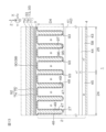
- FIG. 12 is an enlarged view of the portion surrounded by XII in FIG. 2, showing a portion of the multiple IGBT regions 24 and multiple diode regions 25.
- the planar structure of the IGBT regions 24 and diode regions 25 described below may be applied to all the IGBT regions 24 and all the diode regions 25 of the semiconductor chip 2, or may be selectively applied to some of the IGBT regions 24 and diode regions 25.
- the planar structure described below is a structure that can be applied to at least one IGBT region 24 and diode region 25.
- the multiple diode-side trench structures 29 do not cross the gate wiring 13, and have termination portions 32 inside the diode region 25 away from the gate wiring 13 in the second direction Y.
- the second contact layer 39 collectively covers the termination portions 32 of the multiple diode-side trench structures 29.
- the second contact layer 39 is electrically connected to the diode-side trench structures 29 via the termination portions 32.
- the semiconductor device 1 includes a plurality of gate auxiliary trench structures 93 formed on the first main surface 3.
- the plurality of gate auxiliary trench structures 93 are formed directly below the gate extension electrode 33 and are covered by the gate extension electrode 33 in a plan view.
- the plurality of gate auxiliary trench structures 93 are trench structures that are long along the second direction Y.
- the multiple gate-assist trench structures 93 are multiple elliptical trench structures whose major axis direction coincides with the second direction Y.
- the multiple gate-assist trench structures 93 may be formed in a band shape extending along the second direction Y in a plan view.
- the multiple gate-assist trench structures 93 are formed in a stripe shape as a whole.
- the multiple gate-assist trench structures 93 have terminal portions 94 on both one side and the other side of the second direction Y.
- the terminations 94 of the gate auxiliary trench structures 93 are formed for each pair of gate auxiliary trench structures 93.
- the terminations 94 connect adjacent gate auxiliary trench structures 93 in the region directly below the gate extension electrode 33 (boundary region 86 in Figures 10 and 11).
- the terminations 94 are formed in a round shape in a plan view.
- the diode-side trench structure 29 and the gate-assist trench structure 93 are formed on the same imaginary straight line 99 (shown by a dashed line in FIG. 12) extending along the second direction Y. Therefore, the gate-assist trench structure 93 may be a trench structure formed on an extension of the diode-side trench structure 29 in the second direction Y.
- the first electrode layer 34 of the gate extension electrode 33 is formed in a strip shape that continuously extends across the alternatingly arranged IGBT regions 24 and diode regions 25.
- the first electrode layer 34 is strip-shaped with a constant width in the second direction Y.
- the first electrode layer 34 is disposed directly below the second electrode layer 35 in both the non-contact section 36 and the contact section 37.
- the first electrode layer 34 collectively covers the multiple trench gate structures 27 and the multiple gate auxiliary trench structures 93. In this form, the entire gate auxiliary trench structure 93 from one end to the other end in the second direction Y is covered by the first electrode layer 34.
- FIG. 13 is a cross-sectional view taken along line XIII-XIII in FIG. 12.
- structures that correspond to structures already described with respect to the semiconductor device 1 will be given the same reference numerals and will not be described.
- the gate auxiliary trench structure 93 includes a gate auxiliary trench 95, a gate auxiliary insulating layer 96, and a gate auxiliary electrode layer 97.
- the gate auxiliary trench 95 is formed on the first main surface 3 of the semiconductor chip 2.
- the gate auxiliary trench 95 includes a sidewall and a bottom wall. The sidewall of the gate auxiliary trench 95 may be formed perpendicular to the first main surface 3.
- the sidewall of the gate auxiliary trench 95 may be inclined downward from the first main surface 3 toward the bottom wall.
- the gate auxiliary trench 95 may be formed in a tapered shape in which the opening area on the opening side is larger than the bottom area.
- the well region 87 is exposed from the sidewall of the gate auxiliary trench 95.
- the bottom wall of the gate auxiliary trench 95 may be formed parallel to the first main surface 3.
- the bottom wall of the gate auxiliary trench 95 may be formed in a curved shape toward the second main surface 4.
- the gate auxiliary trench 95 includes a bottom wall edge portion.
- the bottom wall edge portion connects the sidewall and bottom wall of the gate auxiliary trench 95.
- the bottom wall edge portion may be formed in a curved shape toward the second main surface 4 of the semiconductor chip 2.
- the depth D4 of the gate auxiliary trench 95 may be 2 ⁇ m or more and 10 ⁇ m or less.
- the depth D4 of the gate auxiliary trench 95 may be 2 ⁇ m or more and 3 ⁇ m or less, 3 ⁇ m or more and 4 ⁇ m or less, 4 ⁇ m or more and 5 ⁇ m or less, 5 ⁇ m or more and 6 ⁇ m or less, 6 ⁇ m or more and 7 ⁇ m or less, 8 ⁇ m or more and 9 ⁇ m or less, or 9 ⁇ m or more and 10 ⁇ m or less.
- the depth D4 of the gate auxiliary trench 95 may be equal to the depth D1 of the gate trench 47.
- the width of the gate auxiliary trench 95 may be 0.5 ⁇ m or more and 3 ⁇ m or less.
- the width of the gate auxiliary trench 95 is the width of the gate auxiliary trench 95 in the first direction X.
- the width of the gate auxiliary trench 95 may be 0.5 ⁇ m or more and 1 ⁇ m or less, 1 ⁇ m or more and 1.5 ⁇ m or less, 1.5 ⁇ m or more and 2 ⁇ m or less, 2 ⁇ m or more and 2.5 ⁇ m or less, or 2.5 ⁇ m or more and 3 ⁇ m or less.
- the width of the gate auxiliary trench 95 may be equal to the width of the gate trench 47.
- the gate auxiliary insulating layer 96 is formed in the form of a film along the inner wall of the gate auxiliary trench 95.
- the gate auxiliary insulating layer 96 defines a recess space within the gate auxiliary trench 95.
- the gate auxiliary insulating layer 96 includes a silicon oxide film.
- the gate auxiliary insulating layer 96 may include a silicon nitride film instead of or in addition to the silicon oxide film.
- the gate auxiliary electrode layer 97 is embedded in the gate auxiliary trench 95 with the gate auxiliary insulating layer 96 sandwiched therebetween. Specifically, the gate auxiliary electrode layer 97 is embedded in a recess space defined by the gate auxiliary insulating layer 96 in the gate auxiliary trench 95.
- the gate auxiliary electrode layer 97 may include conductive polysilicon. The gate auxiliary electrode layer 97 is controlled to the gate potential.
- the extraction electrode layer 90 extended from the gate trench 47 onto the first main surface 3 is integrally connected to the gate auxiliary electrode layer 97.
- the extraction electrode layer 90 is extended onto the first main surface 3 integrally from the gate electrode layer 49 and the gate auxiliary electrode layer 97, and collectively covers the gate trench 47 and the gate auxiliary trench 95.
- each gate-assist trench structure 93 may be formed in an independent strip shape.
- Each gate-assist trench structure 93 is a strip-shaped trench structure whose length direction coincides with the second direction Y.
- the end portions 98 of each gate-assist trench structure 93 are positioned inside both side edges of the first electrode layer 34 in the second direction Y, and are covered by the first electrode layer 34.
- each gate-assist trench structure 93 may be formed in independent strips.
- Each gate-assist trench structure 93 is a strip-shaped trench structure whose length direction coincides with the second direction Y.
- the end portions 98 of each gate-assist trench structure 93 protrude outward beyond both side edges of the first electrode layer 34 in the second direction Y, and are exposed from the first electrode layer 34.
- the multiple gate-assist trench structures 93 are long trench structures along the first direction X.
- the elliptical trench structure of FIG. 12 is rotated by 90°, but of course the strip-shaped trench structure of FIG. 14 and FIG. 15 may also be rotated by 90°.
- multiple gate auxiliary trench structures 93 controlled by the gate potential are formed. This allows the gate capacitance to be increased, thereby improving the ESD tolerance of the gate. Furthermore, the multiple gate auxiliary trench structures 93 are arranged in the empty space directly below the gate extension electrode 33 sandwiched between the multiple diode-side trench structures 29. This makes it possible to avoid an increase in chip area or gate trench density due to the gate auxiliary trench structures 93. This makes it possible to suppress an increase in chip costs and an increase in process difficulty.
- the gate extension electrode 33 can be reliably connected to the gate auxiliary trench structure 93 even if the gate extension electrode 33 is misaligned in the second direction Y.
- FIG. 17 is an enlarged view of the portion surrounded by XVII in FIG. 2, showing a portion of the multiple IGBT regions 24 and multiple diode regions 25.
- the planar structure of the IGBT regions 24 and diode regions 25 described below may be applied to all the IGBT regions 24 and all the diode regions 25 of the semiconductor chip 2, or may be selectively applied to some of the IGBT regions 24 and diode regions 25.
- the planar structure described below is a structure that can be applied to at least one IGBT region 24 and diode region 25.
- the first end (the end on the side surface 5B side) of the RC-IGBT array 26 is formed by a diode region 25.
- This diode region 25 is adjacent to a plurality of terminal electrodes 7 to 11, and may be referred to as a pad-adjacent diode region 25A.
- the pad-adjacent diode region 25A is adjacent to the gate terminal electrode 7 in the first direction X. "Adjacent to the gate terminal electrode 7" may mean that no other diode region 25 or IGBT region 24 is interposed between the gate terminal electrode 7 and the pad-adjacent diode region 25A in the first direction X.
- the multiple diode-side trench structures 29 do not cross the gate wiring 13, and have termination portions 32 inside the diode region 25 away from the gate wiring 13 in the second direction Y.
- the second contact layer 39 collectively covers the termination portions 32 of the multiple diode-side trench structures 29.
- the second contact layer 39 is electrically connected to the diode-side trench structures 29 via the termination portions 32.
- the gate extension electrode 33 includes a ring-shaped peripheral portion 100 that surrounds the gate terminal electrode 7, and an extension portion 101 that extends in a strip shape from the peripheral portion 100 in the first direction X.
- the peripheral portion 100 surrounds the entire periphery of the gate terminal electrode 7, but may be partially separated.
- the end of the peripheral portion 100 on the side surface 5B side is integrally connected to the first portion 16 of the gate wiring 13.
- An annular gap region 102 is formed between the peripheral portion 100 and the gate terminal electrode 7.
- the extension portion 101 extends in the first direction X from the end of the peripheral portion 100 opposite the end on the side surface 5B side.
- the extension portion 101 extends in a band shape in the first direction X.
- the peripheral portion 100 and the extension portion 101 are formed by a laminated structure of a resistive layer 103 and a wiring layer 104.
- the lower resistive layer 103 of the laminated structure is the white region, and the upper wiring layer 104 is the hatched region.
- the resistive layer 103 also serves as the first electrode layer 34 and first contact layer 38 described above.
- the wiring layer 104 also serves as the second electrode layer 35 described above.
- the laminated structure of the resistive layer 103 and the wiring layer 104 may form the gate extension electrode 33, and a part of it may form the gate terminal electrode 7.
- a part of the resistive layer 103 forms an island-shaped pad support layer 105, and the peripheral portion 100 and the second electrode layer 35 that forms the gate terminal electrode 7 are formed independently of each other on the pad support layer 105.
- the second electrode layer 35 of the peripheral portion 100 is connected to the pad support layer 105 via the peripheral contacts 106.
- a pair of peripheral contacts 106 are formed facing each other across the gate terminal electrode 7 in the first direction X.
- the pair of peripheral contacts 106 are formed one at each of the end of the peripheral portion 100 on the side surface 5B side and the opposite end.
- the second electrode layer 35 of the gate terminal electrode 7 is connected to the pad support layer 105 via pad contacts 107.
- a pair of pad contacts 107 are formed adjacent to the peripheral contacts 106 in the first direction X.
- the pair of pad contacts 107 are formed one at a time at a position adjacent to each peripheral contact 106.
- the semiconductor device 1 includes a gate resistor 108 adjacent to the gate terminal electrode 7.
- the gate resistor 108 is selectively formed in a portion of the gate extension electrode 33 that crosses the diode region 25, avoiding the portion directly above the trench gate structure 27.
- the gate resistor 108 is formed in the extension portion 101 at a position adjacent to the terminal end 32 of the diode-side trench structure 29 in the second direction Y. More specifically, the gate resistor 108 is formed in a region sandwiched between a plurality of diode-side trench structures 29 that face each other across the gate extension electrode 33.
- the wiring layer 104 of the gate extension electrode 33 (extension portion 101) is divided into one side and the other side in the first direction X.
- the gate resistor 108 is formed by a portion of the resistance layer 103 sandwiched between the divided wiring layers 104.
- the extension portion 101 includes a first extension portion 109 close to the gate terminal electrode 7 and a second extension portion 110 on the opposite side.
- the first extension portion 109 and the second extension portion 110 are each connected to the resistive layer 103 via a resistive contact 111.
- the gate resistor 108 is disposed between the first extension portion 109 and the second extension portion 110.
- the gate resistor 108 is formed in a band shape of a constant width in a plan view, extending in the first direction X.
- the gate resistor 108 may further include a plurality of trench resistor structures 112.
- the plurality of trench resistor structures 112 are formed in the shape of long stripes in the second direction Y between the first extension portion 109 and the second extension portion 110.
- Each trench resistor structure 112 is formed in the shape of a long strip in a plan view in a direction crossing the gate extension electrode 33.
- FIG. 18 is a cross-sectional view taken along line XVIII-XVIII of FIG. 17.
- FIG. 19 is a cross-sectional view taken along line XIX-XIX of FIG. 17.
- a well region 87 extends directly below the gate terminal electrode 7.
- a pad support layer 105 (resistance layer 103, first electrode layer 34) is formed in the well region 87 via a first insulating layer 68.
- the pad support layer 105 is covered by a third insulating layer 70.
- the peripheral contact 106 and the pad contact 107 are embedded in the third insulating layer 70.
- the peripheral contact 106 and the pad contact 107 may be referred to as a peripheral plug electrode and a pad plug electrode, respectively.
- the peripheral contact 106 and the pad contact 107 have a structure corresponding to the emitter plug electrode 73.
- the explanation of the peripheral contact 106 and the pad contact 107 is to be applied mutatis mutandis to the explanation of the emitter plug electrode 73.
- the structures of the peripheral contact 106 and the pad contact 107 that correspond to the structure described for the emitter plug electrode 73 are given the same reference numerals and will not be explained.
- the gate terminal electrode 7 and the peripheral portion 100 are formed on the third insulating layer 70.
- the gate terminal electrode 7 and the peripheral portion 100 are electrically connected to each other via the pad contact 107, the pad support layer 105, and the peripheral contact 106.
- a trench resistor structure 112 is formed on the first main surface 3.
- the trench resistor structure 112 includes a resistive trench 113, a resistive insulating layer 114, and a resistive electrode layer 115.
- the resistive trench 113 is formed in the first main surface 3 of the semiconductor chip 2.
- the resistive trench 113 includes a sidewall and a bottom wall. The sidewall of the resistive trench 113 may be formed perpendicular to the first main surface 3.
- the sidewall of the resistive trench 113 may be inclined downward from the first main surface 3 toward the bottom wall.
- the resistive trench 113 may be formed in a tapered shape in which the opening area on the opening side is larger than the bottom area.
- the well region 87 is exposed from the sidewall of the resistive trench 113.
- the bottom wall of the resistive trench 113 may be formed parallel to the first main surface 3.
- the bottom wall of the resistive trench 113 may be formed in a curved shape toward the second main surface 4.
- the resistive trench 113 includes a bottom wall edge portion.
- the bottom wall edge portion connects the sidewall and bottom wall of the resistive trench 113.
- the bottom wall edge portion may be formed in a curved shape toward the second main surface 4 of the semiconductor chip 2.
- the depth D5 of the resistive trench 113 may be 2 ⁇ m or more and 10 ⁇ m or less.
- the depth D5 of the resistive trench 113 may be 2 ⁇ m or more and 3 ⁇ m or less, 3 ⁇ m or more and 4 ⁇ m or less, 4 ⁇ m or more and 5 ⁇ m or less, 5 ⁇ m or more and 6 ⁇ m or less, 6 ⁇ m or more and 7 ⁇ m or less, 8 ⁇ m or more and 9 ⁇ m or less, or 9 ⁇ m or more and 10 ⁇ m or less.
- the depth D5 of the resistive trench 113 may be equal to the depth D1 of the gate trench 47.
- the width of the resistive trench 113 may be 0.5 ⁇ m or more and 3 ⁇ m or less.
- the width of the resistive trench 113 is the width of the resistive trench 113 in the first direction X.
- the width of the resistive trench 113 may be 0.5 ⁇ m or more and 1 ⁇ m or less, 1 ⁇ m or more and 1.5 ⁇ m or less, 1.5 ⁇ m or more and 2 ⁇ m or less, 2 ⁇ m or more and 2.5 ⁇ m or less, or 2.5 ⁇ m or more and 3 ⁇ m or less.
- the width of the resistive trench 113 may be equal to the width of the gate trench 47.
- the resistive insulating layer 114 is formed in the form of a film along the inner wall of the resistive trench 113.
- the resistive insulating layer 114 defines a recess space within the resistive trench 113.
- the resistive insulating layer 114 includes a silicon oxide film.
- the resistive insulating layer 114 may include a silicon nitride film instead of or in addition to the silicon oxide film.
- the resistive electrode layer 115 is embedded in the resistive trench 113 with the resistive insulating layer 114 sandwiched therebetween. Specifically, the resistive electrode layer 115 is embedded in a recess space defined by the resistive insulating layer 114 in the resistive trench 113.
- the resistive electrode layer 115 may include conductive polysilicon. The resistive electrode layer 115 is controlled to the gate potential.
- the gate resistor 108 has an extraction resistive layer 116 that is pulled out from the resistive trench 113 onto the first main surface 3.
- the extraction resistive layer 116 is integrally connected to the resistive electrode layer 115.
- the extraction electrode layer 90 is integrally pulled out from the resistive electrode layer 115 onto the first main surface 3, and collectively covers the multiple resistive trenches 113.
- the pad support layer 105 is covered by the third insulating layer 70.
- the resistor contact 111 is embedded in the third insulating layer 70.
- the resistor contact 111 may be referred to as a resistor plug electrode.
- the resistor contact 111 has a structure corresponding to the emitter plug electrode 73.
- the explanation of the resistor contact 111 is the same as that of the emitter plug electrode 73.
- the structure of the resistor contact 111 that corresponds to the structure described for the emitter plug electrode 73 is given the same reference numerals and the explanation is omitted.
- a first extension portion 109 and a second extension portion 110 are formed on the third insulating layer 70.
- the first extension portion 109 and the second extension portion 110 are electrically connected to each other via a resistive contact 111, an extraction resistive layer 116, and a resistive electrode layer 115.
- the portion of the resistive layer 103 where the first extension portion 109 and the second extension portion 110 are laminated is short-circuited by the first extension portion 109 and the second extension portion 110 formed by the wiring layer 104, which has a lower resistance than the resistive layer 103.
- the portion of the resistive layer 103 exposed between the first extension portion 109 and the second extension portion 110 forms the gate resistor 108.
- FIG. 20 is a diagram showing a modified arrangement pattern of the IGBT regions 24 and the diode regions 25.
- FIG. 21 is an enlarged view of the portion surrounded by XXI in FIG. 20.
- the first end (the end on the side surface 5B side) of the RC-IGBT array 26 is formed by a diode region 25.
- This diode region 25 is adjacent to the multiple terminal electrodes 7 to 11, and may be referred to as a pad-adjacent diode region 25A.
- the pad-adjacent diode region 25A is adjacent to the gate terminal electrode 7 in the second direction Y.
- the gate resistor 108 is selectively formed in the gate extension electrode 33 in a portion that crosses the diode region 25, avoiding the portion directly above the trench gate structure 27.
- the gate resistor 108 is formed in the peripheral portion 100 at a position adjacent to the end portion 32 of the diode-side trench structure 29 in the second direction Y. More specifically, the gate resistor 108 is formed in a region sandwiched between a plurality of diode-side trench structures 29 that face each other across the gate terminal electrode 7 and the peripheral portion 100. A pair of gate resistors 108 face each other in the second direction Y, sandwiching the gate terminal electrode 7 therebetween.
- the wiring layer 104 of the gate extension electrode 33 (peripheral portion 100) is divided into one side and the other side in the first direction X.
- the gate resistor 108 is formed by a portion of the resistance layer 103 (pad support layer 105) sandwiched between the divided wiring layers 104.
- the peripheral portion 100 includes a first peripheral portion 117 that is connected to the first portion 16 of the gate wiring 13, and a second peripheral portion 118 on the opposite side.
- the first peripheral portion 117 and the second peripheral portion 118 are each connected to the resistive layer 103 via a resistive contact 111.
- the gate resistor 108 is disposed between the first peripheral portion 117 and the second peripheral portion 118.
- the gate resistor 108 is formed in a band shape of a constant width in a plan view, extending in the first direction X.
- the gate resistor 108 may further include a plurality of trench resistor structures 112.
- the plurality of trench resistor structures 112 are formed in the shape of long stripes in the second direction Y between the first peripheral portion 117 and the second peripheral portion 118.
- Each trench resistor structure 112 is formed in the shape of a long strip in a plan view in a direction crossing the gate extension electrode 33.
- the gate resistor 108 is formed on the gate extension electrode 33.
- the gate resistor 108 constitutes a gate resistance for the gate of the IGBT.
- the gate resistor 108 is effective in suppressing oscillation (noise) caused by parasitic inductance at turn-off.
- the gate resistor 108 is disposed in the empty space directly below the gate extension electrode 33 sandwiched between multiple diode-side trench structures 29. This makes it possible to avoid an increase in chip area due to the gate resistor 108. Therefore, it is possible to provide a semiconductor device 1 having a gate resistor 108 without compromising the effective area of the IGBT region 24.
- the p-type portion may be formed as n-type
- the n-type portion may be formed as p-type
- a chip (2) having a first major surface (3) and a second major surface (4); An insulating layer (67) covering the first main surface (3); an extended electrode (33) extending in a first direction (X) in a region on the first main surface (3), the extended electrode (33) including a first electrode layer (34) formed between the insulating layer (67) and the first main surface (3), and a second electrode layer (35) formed on the insulating layer (67) and electrically connected to the first electrode layer (34); a first element region (24) including an element electrically connected to the extension electrode (33); a second element region (25) adjacent to the first element region (24) in the first direction (X) and formed on one side and the other side of the extension electrode (33) in a second direction (Y) intersecting the first direction (X); a second trench electrode structure (29) formed on the first main surface (3) of the chip (2), crossing the extension electrode (33) and spanning a plurality of the second element regions (25) adjacent to each other with the extension electrode (33) interposed therebetween;
- the second trench electrode structure (29) crosses the extension electrode (33) and spans multiple adjacent second element regions (25) across the extension electrode (33). In other words, the second trench electrode structure (29) is not divided into second element regions (25). This makes it possible to reduce the number of terminations of the second trench electrode structure (29).
- the end of the second trench electrode structure (29) is rounded, shape abnormalities are likely to occur due to variations in the recess. Therefore, by reducing the number of end parts of the second trench electrode structure (29), it is possible to suppress insulation breakdown at the end parts. As a result, it is possible to improve the ESD (Electro-Static Discharge) tolerance of the semiconductor device (1).
- ESD Electro-Static Discharge
- the first element region (24) is formed on one side and the other side of the extension electrode (33) in the second direction (Y), a first trench electrode structure (27) formed on the first main surface (3) of the chip (2), crossing the extension electrode (33), spanning a plurality of the first element regions (24) adjacent to each other with the extension electrode (33) in between, and being physically and electrically isolated from the second trench electrode structure (29);
- the semiconductor device (1) described in Appendix 1-2 includes a second electrode layer (35) extending continuously across the plurality of first element regions (24) and the plurality of second element regions (25), and a plurality of first electrode layers (34) selectively arranged in contact sections (37) where the second electrode layer (35) and the first element region (24) are opposed to each other by being selectively divided at non-contact sections (36) where the second electrode layer (35) and the second element region (25) are opposed to each other.
- the first trench electrode structure (27) includes a first trench (47) and a first buried electrode (49) buried in the first trench (47);
- the second trench electrode structure (29) includes a second trench (61) and a second buried electrode (63) buried in the second trench (61) and covered by the insulating layer (67);
- the semiconductor device (1) described in Appendix 1-4 further includes a second contact layer (39) that is formed adjacent to the extended electrode (33) in the second direction (Y), is integrally drawn out from the second buried electrode (63) onto the first main surface (3), and collectively covers the multiple second trench electrode structures (29).
- the semiconductor device (1) described in Appendix 1-5 further includes a third trench electrode structure (28) that extends in parallel with the first trench electrode structure (27) in the first element region (24), does not cross the extension electrode (33), and has a terminal portion (31) inside the first element region (24) away from the extension electrode (33) in the second direction (Y).
- the third trench electrode structure (28) includes a third trench (55) and a third buried electrode (57) buried in the third trench (55) and covered by the insulating layer (67); a third contact layer (40) extended integrally from the third buried electrode (57) onto the first main surface (3) at the termination portion (31) of the third trench electrode structure (28);
- the semiconductor device (1) described in Appendix 1-7 further includes a surface electrode layer (12) covering the second contact layer (39) and the third contact layer (40) and connected to the second contact layer (39) and the third contact layer (40).
- a plurality of the extension electrodes (33) are formed at intervals in the second direction (Y), The semiconductor device (1) described in Appendix 1-8, wherein the surface electrode layer (12) covers at least one of the first element regions (24) and one of the second element regions (25) in a partition region (20) sandwiched between adjacent extended electrodes (33).
- the first element region (24) includes an IGBT region (24) having a body region (50) of a second conductivity type formed on the first main surface (3), an emitter region (51) of a first conductivity type formed in a surface layer portion of the body region (50), a collector region (45) of a second conductivity type formed on the second main surface (4), and a trench gate structure (27) as the first trench electrode structure (27);
- the second element region (25) includes a diode region (25) having a first impurity region (64) of a second conductivity type formed in the first main surface (3), a second impurity region (58) of a first conductivity type formed in the second main surface (4), and a diode-side trench structure (29) as the second trench electrode structure (29) electrically connected to the emitter region (51);
- the semiconductor device (1) according to any one of Supplementary Note 1-2 to Supplementary Note 1-9, wherein the extension electrode (33) includes
- the semiconductor device (1) described in appendix 1-10 includes a well region (87) of a second conductivity type formed on the first main surface (3) directly below the gate extension electrode (33) and deeper than the trench gate structure (27) and the diode-side trench structure (29).
- Appendix 1-12 The semiconductor device (1) described in Appendix 1-11, wherein the well region (87) spans a boundary between the IGBT region (24) and the diode region (25) in the first direction (X), crosses the gate extension electrode (33) in the second direction (Y), and is integrally connected to the body region (50) of the IGBT region (24) and the first impurity region (64) of the diode region (25).
- the semiconductor device (1) according to any one of Appendices 1-10 to 1-12, wherein the gate extension electrode (33) selectively has a gate resistor (108) in a portion adjacent to the fourth trench electrode structure (29).
- the semiconductor device further includes a gate pad electrode (7) electrically connected to the gate extension electrode (33),
- the diode region (25A) is adjacent to the gate pad electrode (7) in the first direction (X) and includes a pad-adjacent diode region (25A) in which the fourth trench electrode structure (29) is formed,
- the gate extension electrode (33) includes a plurality of the second electrode layers (35, 109, 110) that are divided in a portion crossing the pad-adjacent diode region (25A);
- the semiconductor device (1) according to appendix 1-13, wherein the gate resistor (108) is formed by a portion of the first electrode layer (34) sandwiched between the plurality of second electrode layers (35, 109, 110).
- the semiconductor device further includes a gate pad electrode (7) electrically connected to the gate extension electrode (33), the diode region (25) is adjacent to the gate pad electrode (7) in the second direction (Y) and includes a pad-adjacent diode region (25) in which the fourth trench electrode structure (29) is formed; the gate extension electrode (33) includes a plurality of the second electrode layers (35, 109, 110) that are divided in a portion crossing the pad-adjacent diode region (25);
- the semiconductor device (1) according to appendix 1-13, wherein the gate resistor (108) is formed by a portion of the first electrode layer (34) sandwiched between the plurality of second electrode layers (35, 109, 110).
- the gate extension electrode (33) selectively has a gate resistor (108) in a portion crossing the diode region (25) while avoiding a portion directly above the trench gate structure (27).
- the gate extension electrode (33) has a gate resistor (108).
- the gate resistor (108) constitutes a gate resistance for the gate of the IGBT.
- the gate resistor (108) is effective in suppressing oscillation (noise) caused by parasitic inductance at turn-off.
- the gate resistor (108) is selectively arranged in a portion of the gate extension electrode (33) that crosses the diode region (25) while avoiding the portion directly above the trench gate structure (27). Therefore, it is possible to avoid an increase in the chip (2) area due to the gate resistor (108). Therefore, it is possible to provide a semiconductor device (1) having a gate resistor (108) without impairing the effective area of the IGBT region (24).
- the gate extension electrode (33) includes a resistance layer (103) formed between the insulating layer (67) and the first main surface (3) and extending continuously across the IGBT region (24) and the diode region (25) in the first direction (X), and a plurality of wiring layers (104) formed on the insulating layer (67), divided at a portion crossing the diode region (25), and having a lower resistance than the resistance layer (103);
- the trench gate structure (27) includes a gate trench (47) and a gate buried electrode (49) buried in the gate trench (47);
- the gate extension electrode (33) includes an annular peripheral portion (100) surrounding the gate pad electrode (7) and an extension portion (101) extending in a strip shape from the peripheral portion (100) in the first direction (X),
- the diode region (25) includes a pad-adjacent diode region (25A) adjacent to the gate pad electrode (7) in the first direction (X), a diode-side trench structure (29) formed in the pad-adjacent diode region (25A) and having a termination portion (32) inside the pad-adjacent diode region (25A) away from the extension portion (101) in a second direction (Y) intersecting the first direction (X);
- the semiconductor device (1) according to any one of Supplementary Notes 2-1 to 2-5, wherein the gate resistor (108) is formed adjacent to the termination portion (32) of the diode-side trench structure (29) in the extension portion (101).
- a plurality of the IGBT regions (24) and a plurality of the diode regions (25) are alternately arranged in the first direction (X),
- the pad-adjacent diode region (25A) is selectively formed in a portion adjacent to the gate pad electrode (7) in the first direction (X),
- the gate pad electrode (7) is disposed on the periphery of the chip (2),
- the gate extension electrode (33) is formed from the gate pad electrode (7) along the periphery of the chip (2) and includes an outer extension electrode (16) surrounding an active area (18), and an inner extension electrode (17, 33) that crosses the active area (18) and has one end and the other end connected to different positions on the outer extension electrode (16),
- the semiconductor device (1) according to claim 2-6 or 2-7, wherein the gate resistor (108) is formed on the inner extension electrode (17, 33).
- the gate extension electrode (33) includes an annular peripheral portion (100) surrounding the gate pad electrode (7) and an extension portion (101) extending in a strip shape from the peripheral portion (100) in the first direction (X),
- the diode region (25) includes a pad-adjacent diode region (25A) adjacent to the gate pad electrode (7) in a second direction (Y) intersecting the first direction (X), a diode-side trench structure (29) formed in the pad-adjacent diode region (25A) and having a termination portion (32) inside the pad-adjacent diode region (25A) away from the periphery portion (100) in the second direction (Y);
- the semiconductor device (1) according to any one of Appendix 2-1 to Appendix 2-5, wherein the gate resistor (108) is formed adjacent to the terminal portion (32) of the diode-side trench structure (29) in the peripheral portion (100) of the gate extension electrode (33
- a plurality of the IGBT regions (24) and a plurality of the diode regions (25) are alternately arranged in the first direction (X),
- the pad-adjacent diode region (25A) is selectively formed in a portion adjacent to the gate pad electrode (7) in the second direction (Y),
- a gate auxiliary buried electrode (97) is formed that is electrically connected to the gate extension electrode (33). This increases the gate capacitance, thereby improving the ESD tolerance of the gate.
- the gate auxiliary buried electrode (97) is disposed in the empty space directly below the gate extension electrode (33). This makes it possible to avoid an increase in the chip (2) area or an increase in the density of the gate trenches (47) due to the gate auxiliary buried electrode (97). This makes it possible to suppress an increase in chip costs and an increase in process difficulty.
- the trench gate structure (27) includes a gate trench (47) and a gate buried electrode (49) buried in the gate trench (47);
- the semiconductor device (1) according to any one of Appendix 3-1 to Appendix 3-5, wherein the gate extension electrode (33) includes a first electrode layer (34) that is integrally drawn out from the gate buried electrode (49) and the gate auxiliary buried electrode (97) onto the first main surface (3) and collectively covers the gate trench (47) and the gate auxiliary trench (95), and a second electrode layer (35) that is formed on the first electrode layer (34) via an insulating layer (67) and extends in the first direction (X) across the gate trench (47) and the gate auxiliary trench (95).
- the first electrode layer (34) is in a strip shape extending with a constant width in the first direction (X)
- the semiconductor device (1) according to any one of Appendices 3-1 to 3-7, wherein the second element region (25) includes a diode region (25) having a first impurity region (64) of a second conductivity type formed in the first main surface (3), a second impurity region (58) of a first conductivity type formed in the second main surface (4), and a diode-side trench structure (29) as the second trench electrode structure (29) electrically connected to the emitter region (51).
- the gate extension electrode (33) includes a resistance layer (103) formed between the insulating layer (67) and the first main surface (3) and extending continuously across the IGBT region (24) and the diode region (25) in the first direction (X), and a plurality of wiring layers (104) formed on the insulating layer (67), divided at a portion crossing the diode region (25), and having a lower resistance than the resistance layer (103);
- the semiconductor device further includes a gate pad electrode (7) electrically connected to the gate extension electrode (33),
- the diode region (25) includes a pad-adjacent diode region (25A) adjacent to the gate pad electrode (7) in the first direction (X),
- the semiconductor device (1) according to any one of appendices 3-10 to 3-13, wherein the gate resistor (108) is formed in the gate extension electrode (33) at a position adjacent to the pad-adjacent diode region (25A).
- the semiconductor device further includes a gate pad electrode (7) electrically connected to the gate extension electrode (33),
- the diode region (25) includes a pad-adjacent diode region (25A) adjacent to the gate pad electrode (7) in the second direction (Y),
- the semiconductor device (1) according to any one of Supplementary Notes 3-10 to 3-13, wherein the gate resistor (108) is formed in the gate extension electrode (33) at a position adjacent to the pad-adjacent diode region (25A).
Landscapes
- Metal-Oxide And Bipolar Metal-Oxide Semiconductor Integrated Circuits (AREA)
- Electrodes Of Semiconductors (AREA)
Priority Applications (2)
| Application Number | Priority Date | Filing Date | Title |
|---|---|---|---|
| JP2025521934A JPWO2024241882A1 (https=) | 2023-05-22 | 2024-05-08 | |
| US19/396,386 US20260082683A1 (en) | 2023-05-22 | 2025-11-21 | Semiconductor device |
Applications Claiming Priority (2)
| Application Number | Priority Date | Filing Date | Title |
|---|---|---|---|
| JP2023-084042 | 2023-05-22 | ||
| JP2023084042 | 2023-05-22 |
Related Child Applications (1)
| Application Number | Title | Priority Date | Filing Date |
|---|---|---|---|
| US19/396,386 Continuation US20260082683A1 (en) | 2023-05-22 | 2025-11-21 | Semiconductor device |
Publications (1)
| Publication Number | Publication Date |
|---|---|
| WO2024241882A1 true WO2024241882A1 (ja) | 2024-11-28 |
Family
ID=93589174
Family Applications (1)
| Application Number | Title | Priority Date | Filing Date |
|---|---|---|---|
| PCT/JP2024/017129 Ceased WO2024241882A1 (ja) | 2023-05-22 | 2024-05-08 | 半導体装置 |
Country Status (3)
| Country | Link |
|---|---|
| US (1) | US20260082683A1 (https=) |
| JP (1) | JPWO2024241882A1 (https=) |
| WO (1) | WO2024241882A1 (https=) |
Citations (5)
| Publication number | Priority date | Publication date | Assignee | Title |
|---|---|---|---|---|
| JP2009206478A (ja) * | 2008-01-28 | 2009-09-10 | Fuji Electric Device Technology Co Ltd | 半導体装置 |
| WO2019098271A1 (ja) * | 2017-11-16 | 2019-05-23 | 富士電機株式会社 | 半導体装置 |
| WO2021010000A1 (ja) * | 2019-07-12 | 2021-01-21 | 富士電機株式会社 | 半導体装置 |
| US20210119006A1 (en) * | 2019-10-17 | 2021-04-22 | Infineon Technologies Ag | Transistor device with a varying gate runner resistivity per area |
| WO2022201903A1 (ja) * | 2021-03-22 | 2022-09-29 | ローム株式会社 | 半導体装置 |
-
2024
- 2024-05-08 JP JP2025521934A patent/JPWO2024241882A1/ja active Pending
- 2024-05-08 WO PCT/JP2024/017129 patent/WO2024241882A1/ja not_active Ceased
-
2025
- 2025-11-21 US US19/396,386 patent/US20260082683A1/en active Pending
Patent Citations (5)
| Publication number | Priority date | Publication date | Assignee | Title |
|---|---|---|---|---|
| JP2009206478A (ja) * | 2008-01-28 | 2009-09-10 | Fuji Electric Device Technology Co Ltd | 半導体装置 |
| WO2019098271A1 (ja) * | 2017-11-16 | 2019-05-23 | 富士電機株式会社 | 半導体装置 |
| WO2021010000A1 (ja) * | 2019-07-12 | 2021-01-21 | 富士電機株式会社 | 半導体装置 |
| US20210119006A1 (en) * | 2019-10-17 | 2021-04-22 | Infineon Technologies Ag | Transistor device with a varying gate runner resistivity per area |
| WO2022201903A1 (ja) * | 2021-03-22 | 2022-09-29 | ローム株式会社 | 半導体装置 |
Also Published As
| Publication number | Publication date |
|---|---|
| JPWO2024241882A1 (https=) | 2024-11-28 |
| US20260082683A1 (en) | 2026-03-19 |
Similar Documents
| Publication | Publication Date | Title |
|---|---|---|
| JP7207463B2 (ja) | 半導体装置 | |
| US20240178223A1 (en) | Semiconductor device | |
| CN112216691B (zh) | 一种集成箝位二极管的半导体功率器件 | |
| US11664448B2 (en) | Semiconductor device | |
| EP3686929A1 (en) | Semiconductor die | |
| US20240405110A1 (en) | Semiconductor device | |
| US20250380491A1 (en) | Semiconductor device | |
| WO2020246230A1 (ja) | 半導体装置 | |
| US12538508B2 (en) | Semiconductor device | |
| JP2020167230A (ja) | 半導体装置 | |
| WO2024014362A1 (ja) | 半導体装置 | |
| EP4250370A1 (en) | Transistor device | |
| US20250261389A1 (en) | Semiconductor device | |
| WO2024241882A1 (ja) | 半導体装置 | |
| WO2024241883A1 (ja) | 半導体装置 | |
| WO2024241884A1 (ja) | 半導体装置 | |
| JP7472613B2 (ja) | 半導体装置 | |
| JP7424782B2 (ja) | 半導体装置 | |
| CN116018689A (zh) | 半导体装置 | |
| WO2022034828A1 (ja) | 半導体装置 | |
| WO2024202987A1 (ja) | 半導体装置 | |
| WO2025239027A1 (ja) | 半導体装置 | |
| US20250393287A1 (en) | Semiconductor device | |
| US20260011660A1 (en) | Semiconductor device | |
| US20240203835A1 (en) | Semiconductor device |
Legal Events
| Date | Code | Title | Description |
|---|---|---|---|
| 121 | Ep: the epo has been informed by wipo that ep was designated in this application |
Ref document number: 24810890 Country of ref document: EP Kind code of ref document: A1 |
|
| ENP | Entry into the national phase |
Ref document number: 2025521934 Country of ref document: JP Kind code of ref document: A |
|
| NENP | Non-entry into the national phase |
Ref country code: DE |