WO2024237201A1 - 表示装置および電子機器 - Google Patents
表示装置および電子機器 Download PDFInfo
- Publication number
- WO2024237201A1 WO2024237201A1 PCT/JP2024/017432 JP2024017432W WO2024237201A1 WO 2024237201 A1 WO2024237201 A1 WO 2024237201A1 JP 2024017432 W JP2024017432 W JP 2024017432W WO 2024237201 A1 WO2024237201 A1 WO 2024237201A1
- Authority
- WO
- WIPO (PCT)
- Prior art keywords
- electrode
- layer
- display device
- light
- reflective
- Prior art date
- Legal status (The legal status is an assumption and is not a legal conclusion. Google has not performed a legal analysis and makes no representation as to the accuracy of the status listed.)
- Ceased
Links
Images














Classifications
-
- H—ELECTRICITY
- H10—SEMICONDUCTOR DEVICES; ELECTRIC SOLID-STATE DEVICES NOT OTHERWISE PROVIDED FOR
- H10K—ORGANIC ELECTRIC SOLID-STATE DEVICES
- H10K59/00—Integrated devices, or assemblies of multiple devices, comprising at least one organic light-emitting element covered by group H10K50/00
- H10K59/80—Constructional details
- H10K59/875—Arrangements for extracting light from the devices
- H10K59/878—Arrangements for extracting light from the devices comprising reflective means
-
- G—PHYSICS
- G09—EDUCATION; CRYPTOGRAPHY; DISPLAY; ADVERTISING; SEALS
- G09F—DISPLAYING; ADVERTISING; SIGNS; LABELS OR NAME-PLATES; SEALS
- G09F9/00—Indicating arrangements for variable information in which the information is built-up on a support by selection or combination of individual elements
- G09F9/30—Indicating arrangements for variable information in which the information is built-up on a support by selection or combination of individual elements in which the desired character or characters are formed by combining individual elements
-
- G—PHYSICS
- G09—EDUCATION; CRYPTOGRAPHY; DISPLAY; ADVERTISING; SEALS
- G09G—ARRANGEMENTS OR CIRCUITS FOR CONTROL OF INDICATING DEVICES USING STATIC MEANS TO PRESENT VARIABLE INFORMATION
- G09G3/00—Control arrangements or circuits, of interest only in connection with visual indicators other than cathode-ray tubes
- G09G3/20—Control arrangements or circuits, of interest only in connection with visual indicators other than cathode-ray tubes for presentation of an assembly of a number of characters, e.g. a page, by composing the assembly by combination of individual elements arranged in a matrix no fixed position being assigned to or needed to be assigned to the individual characters or partial characters
- G09G3/22—Control arrangements or circuits, of interest only in connection with visual indicators other than cathode-ray tubes for presentation of an assembly of a number of characters, e.g. a page, by composing the assembly by combination of individual elements arranged in a matrix no fixed position being assigned to or needed to be assigned to the individual characters or partial characters using controlled light sources
- G09G3/30—Control arrangements or circuits, of interest only in connection with visual indicators other than cathode-ray tubes for presentation of an assembly of a number of characters, e.g. a page, by composing the assembly by combination of individual elements arranged in a matrix no fixed position being assigned to or needed to be assigned to the individual characters or partial characters using controlled light sources using electroluminescent panels
- G09G3/32—Control arrangements or circuits, of interest only in connection with visual indicators other than cathode-ray tubes for presentation of an assembly of a number of characters, e.g. a page, by composing the assembly by combination of individual elements arranged in a matrix no fixed position being assigned to or needed to be assigned to the individual characters or partial characters using controlled light sources using electroluminescent panels semiconductive, e.g. using light-emitting diodes [LED]
- G09G3/3208—Control arrangements or circuits, of interest only in connection with visual indicators other than cathode-ray tubes for presentation of an assembly of a number of characters, e.g. a page, by composing the assembly by combination of individual elements arranged in a matrix no fixed position being assigned to or needed to be assigned to the individual characters or partial characters using controlled light sources using electroluminescent panels semiconductive, e.g. using light-emitting diodes [LED] organic, e.g. using organic light-emitting diodes [OLED]
- G09G3/3225—Control arrangements or circuits, of interest only in connection with visual indicators other than cathode-ray tubes for presentation of an assembly of a number of characters, e.g. a page, by composing the assembly by combination of individual elements arranged in a matrix no fixed position being assigned to or needed to be assigned to the individual characters or partial characters using controlled light sources using electroluminescent panels semiconductive, e.g. using light-emitting diodes [LED] organic, e.g. using organic light-emitting diodes [OLED] using an active matrix
-
- H—ELECTRICITY
- H10—SEMICONDUCTOR DEVICES; ELECTRIC SOLID-STATE DEVICES NOT OTHERWISE PROVIDED FOR
- H10K—ORGANIC ELECTRIC SOLID-STATE DEVICES
- H10K50/00—Organic light-emitting devices
- H10K50/10—OLEDs or polymer light-emitting diodes [PLED]
-
- H—ELECTRICITY
- H10—SEMICONDUCTOR DEVICES; ELECTRIC SOLID-STATE DEVICES NOT OTHERWISE PROVIDED FOR
- H10K—ORGANIC ELECTRIC SOLID-STATE DEVICES
- H10K50/00—Organic light-emitting devices
- H10K50/10—OLEDs or polymer light-emitting diodes [PLED]
- H10K50/11—OLEDs or polymer light-emitting diodes [PLED] characterised by the electroluminescent [EL] layers
-
- H—ELECTRICITY
- H10—SEMICONDUCTOR DEVICES; ELECTRIC SOLID-STATE DEVICES NOT OTHERWISE PROVIDED FOR
- H10K—ORGANIC ELECTRIC SOLID-STATE DEVICES
- H10K50/00—Organic light-emitting devices
- H10K50/80—Constructional details
- H10K50/805—Electrodes
- H10K50/81—Anodes
- H10K50/813—Anodes characterised by their shape
-
- H—ELECTRICITY
- H10—SEMICONDUCTOR DEVICES; ELECTRIC SOLID-STATE DEVICES NOT OTHERWISE PROVIDED FOR
- H10K—ORGANIC ELECTRIC SOLID-STATE DEVICES
- H10K50/00—Organic light-emitting devices
- H10K50/80—Constructional details
- H10K50/805—Electrodes
- H10K50/81—Anodes
- H10K50/814—Anodes combined with auxiliary electrodes, e.g. ITO layer combined with metal lines
-
- H—ELECTRICITY
- H10—SEMICONDUCTOR DEVICES; ELECTRIC SOLID-STATE DEVICES NOT OTHERWISE PROVIDED FOR
- H10K—ORGANIC ELECTRIC SOLID-STATE DEVICES
- H10K50/00—Organic light-emitting devices
- H10K50/80—Constructional details
- H10K50/805—Electrodes
- H10K50/81—Anodes
- H10K50/818—Reflective anodes, e.g. ITO combined with thick metallic layers
-
- H—ELECTRICITY
- H10—SEMICONDUCTOR DEVICES; ELECTRIC SOLID-STATE DEVICES NOT OTHERWISE PROVIDED FOR
- H10K—ORGANIC ELECTRIC SOLID-STATE DEVICES
- H10K50/00—Organic light-emitting devices
- H10K50/80—Constructional details
- H10K50/805—Electrodes
- H10K50/82—Cathodes
- H10K50/828—Transparent cathodes, e.g. comprising thin metal layers
-
- H—ELECTRICITY
- H10—SEMICONDUCTOR DEVICES; ELECTRIC SOLID-STATE DEVICES NOT OTHERWISE PROVIDED FOR
- H10K—ORGANIC ELECTRIC SOLID-STATE DEVICES
- H10K50/00—Organic light-emitting devices
- H10K50/80—Constructional details
- H10K50/85—Arrangements for extracting light from the devices
- H10K50/856—Arrangements for extracting light from the devices comprising reflective means
-
- H—ELECTRICITY
- H10—SEMICONDUCTOR DEVICES; ELECTRIC SOLID-STATE DEVICES NOT OTHERWISE PROVIDED FOR
- H10K—ORGANIC ELECTRIC SOLID-STATE DEVICES
- H10K59/00—Integrated devices, or assemblies of multiple devices, comprising at least one organic light-emitting element covered by group H10K50/00
- H10K59/10—OLED displays
-
- H—ELECTRICITY
- H10—SEMICONDUCTOR DEVICES; ELECTRIC SOLID-STATE DEVICES NOT OTHERWISE PROVIDED FOR
- H10K—ORGANIC ELECTRIC SOLID-STATE DEVICES
- H10K59/00—Integrated devices, or assemblies of multiple devices, comprising at least one organic light-emitting element covered by group H10K50/00
- H10K59/10—OLED displays
- H10K59/12—Active-matrix OLED [AMOLED] displays
- H10K59/121—Active-matrix OLED [AMOLED] displays characterised by the geometry or disposition of pixel elements
-
- H—ELECTRICITY
- H10—SEMICONDUCTOR DEVICES; ELECTRIC SOLID-STATE DEVICES NOT OTHERWISE PROVIDED FOR
- H10K—ORGANIC ELECTRIC SOLID-STATE DEVICES
- H10K59/00—Integrated devices, or assemblies of multiple devices, comprising at least one organic light-emitting element covered by group H10K50/00
- H10K59/10—OLED displays
- H10K59/12—Active-matrix OLED [AMOLED] displays
- H10K59/122—Pixel-defining structures or layers, e.g. banks
-
- H—ELECTRICITY
- H10—SEMICONDUCTOR DEVICES; ELECTRIC SOLID-STATE DEVICES NOT OTHERWISE PROVIDED FOR
- H10K—ORGANIC ELECTRIC SOLID-STATE DEVICES
- H10K59/00—Integrated devices, or assemblies of multiple devices, comprising at least one organic light-emitting element covered by group H10K50/00
- H10K59/10—OLED displays
- H10K59/12—Active-matrix OLED [AMOLED] displays
- H10K59/131—Interconnections, e.g. wiring lines or terminals
-
- H—ELECTRICITY
- H10—SEMICONDUCTOR DEVICES; ELECTRIC SOLID-STATE DEVICES NOT OTHERWISE PROVIDED FOR
- H10K—ORGANIC ELECTRIC SOLID-STATE DEVICES
- H10K59/00—Integrated devices, or assemblies of multiple devices, comprising at least one organic light-emitting element covered by group H10K50/00
- H10K59/80—Constructional details
- H10K59/805—Electrodes
- H10K59/8051—Anodes
-
- H—ELECTRICITY
- H10—SEMICONDUCTOR DEVICES; ELECTRIC SOLID-STATE DEVICES NOT OTHERWISE PROVIDED FOR
- H10K—ORGANIC ELECTRIC SOLID-STATE DEVICES
- H10K59/00—Integrated devices, or assemblies of multiple devices, comprising at least one organic light-emitting element covered by group H10K50/00
- H10K59/80—Constructional details
- H10K59/805—Electrodes
- H10K59/8052—Cathodes
-
- H—ELECTRICITY
- H10—SEMICONDUCTOR DEVICES; ELECTRIC SOLID-STATE DEVICES NOT OTHERWISE PROVIDED FOR
- H10K—ORGANIC ELECTRIC SOLID-STATE DEVICES
- H10K59/00—Integrated devices, or assemblies of multiple devices, comprising at least one organic light-emitting element covered by group H10K50/00
- H10K59/80—Constructional details
- H10K59/87—Passivation; Containers; Encapsulations
Definitions
- This disclosure relates to a display device and an electronic device equipped with the same.
- Some display devices have an organic-containing layer, including an organic light-emitting layer, that is connected between pixels.
- an organic-containing layer including an organic light-emitting layer
- a reflector structure has been proposed between pixels to increase the light extraction efficiency (see, for example, Patent Document 1).
- the objective of this disclosure is to provide a display device that can suppress abnormal light emission between pixels and an electronic device equipped with the same.
- the display device comprises: A plurality of first electrodes provided for each pixel; At least one reflective electrode disposed between pixels; an organic-containing layer including an organic light-emitting layer provided on the first electrode and connected between pixels; a second electrode provided on the organic material-containing layer; a first portion of the organic material-containing layer located between the pixels protrudes with respect to a second portion of the organic light-emitting layer located within the pixel;
- the reflective electrode is disposed below the protruding second portion, The reflective electrode has a top portion located above the top surface of the first portion.
- the electronic device includes the above-mentioned display device.
- FIG. 1 is a plan view of a display device according to an embodiment.
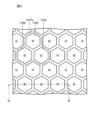
- FIG. 2 is an enlarged plan view showing a part of the effective pixel region.
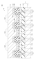
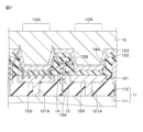
- FIG. 3 is a cross-sectional view taken along line III-III in FIG.
- FIG. 4 is a plan view of a reflective electrode of the display device according to an embodiment.
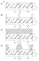
- 5A, 5B, 5C, and 5D are diagrams showing manufacturing steps of a display device according to an embodiment.
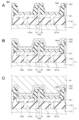
- 6A, 6B, and 6C are diagrams showing manufacturing steps of a display device according to an embodiment.
- FIG. 7 is a cross-sectional view for explaining the function and effect of the display device according to the embodiment.
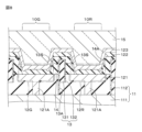
- FIG. 8 is a cross-sectional view of a display device according to the first modification.
- FIG. 9 is a cross-sectional view of a display device according to the first modification.
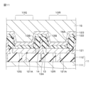
- FIG. 10 is a cross-sectional view of a display device according to the second modification.
- FIG. 11 is a cross-sectional view of a display device according to the second modification.
- FIG. 12 is a cross-sectional view of a display device according to the second modification.
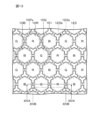
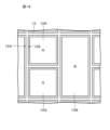
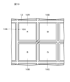
- FIG. 13 is a plan view of a display device according to the third modification.
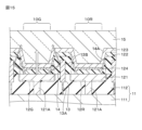
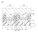
- Fig. 14A is a cross-sectional view taken along line XIVA-XIVA in Fig. 13.
- Fig. 14B is a cross-sectional view taken along line XIVB-XIVB in Fig. 13.
- FIG. 15 is a cross-sectional view of a display device according to the fourth modification.
- FIG. 14A is a cross-sectional view taken along line XIVA-XIVA in Fig. 13.
- Fig. 14B is a cross-sectional view taken along line XIVB-
- FIG. 16 is a cross-sectional view of a display device according to the fifth modification.
- FIG. 17 is a plan view of a reflective electrode of a display device according to the fifth modification.
- FIG. 18 is a plan view of a reflective electrode of a display device according to the sixth modification.
- FIG. 19 is a plan view of a reflective electrode of a display device according to the sixth modification.
- FIG. 20 is a plan view of a reflective electrode of a display device according to the sixth modification.
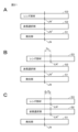
- 21A, 21B, and 21C are conceptual diagrams for explaining the relationship between a normal line LN passing through the center of the light-emitting portion, a normal line LN' passing through the center of the lens member, and a normal line LN" passing through the center of the wavelength selection portion, respectively.
- FIG. 21A, 21B, and 21C are conceptual diagrams for explaining the relationship between a normal line LN passing through the center of the light-emitting portion, a normal line LN' passing through the center of
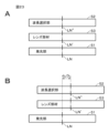
- FIG. 22 is a conceptual diagram for explaining the relationship between a normal line LN passing through the center of the light emitting portion, a normal line LN' passing through the center of the lens member, and a normal line LN" passing through the center of the wavelength selecting portion.
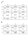
- 23A and 23B are conceptual diagrams for explaining the relationship between a normal line LN passing through the center of the light-emitting portion, a normal line LN' passing through the center of the lens member, and a normal line LN" passing through the center of the wavelength selection portion, respectively.
- FIG. 22 is a conceptual diagram for explaining the relationship between a normal line LN passing through the center of the light emitting portion, a normal line LN' passing through the center of the lens member, and a normal line LN" passing through the center of the wavelength selecting portion, respectively.
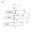
- FIG. 24 is a conceptual diagram for explaining the relationship between a normal line LN passing through the center of the light emitting portion, a normal line LN' passing through the center of the lens member, and a normal line LN" passing through the center of the wavelength selecting portion.
- Fig. 25A is a schematic cross-sectional view for explaining a first example of a resonator structure
- Fig. 25B is a schematic cross-sectional view for explaining a second example of a resonator structure
- 26A and 26B are schematic cross-sectional views for explaining a third example of the resonator structure and a fourth example of the resonator structure, respectively.
- FIGS. 27A and 27B are schematic cross-sectional views for explaining a fifth example of the resonator structure and a sixth example of the resonator structure, respectively.
- FIG. 28 is a schematic cross-sectional view for explaining a seventh example of the resonator structure.
- 29A and 29B are front and rear views of the digital still camera.
- FIG. 30 is a perspective view of a head mounted display.
- FIG. 31 is a perspective view of a television device.
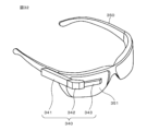
- FIG. 32 is a perspective view of a see-through head mounted display.
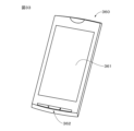
- FIG. 33 is a perspective view of a smartphone.
- Fig. 34A is a diagram showing the interior of the vehicle from the rear to the front
- Fig. 34B is a diagram showing the interior of the vehicle from the diagonally rear to the diagonally front.
- One embodiment> [Schematic configuration of display device 101] 1 is a plan view of a display device 101 according to an embodiment of the present invention.
- the display device 101 has an effective pixel region RE1 and a peripheral region RE2 provided around the effective pixel region RE1.
- FIG. 2 is a plan view showing an enlarged portion of the effective pixel region RE1.
- a plurality of pixels 10R, a plurality of pixels 10G, and a plurality of pixels 10B are provided in the effective pixel region RE1.
- the plurality of pixels 10 are two-dimensionally arranged in a prescribed arrangement pattern. In one embodiment, the arrangement pattern of the plurality of pixels 10 may be a delta arrangement.
- a pad section 11a and a driver (not shown) for displaying images, etc. are provided in the peripheral region RE2.
- a flexible printed circuit (FPC) (not shown) may be connected to the pad section 11a.
- Pixels 10R, 10G, and 10B have different colors.
- Pixel 10R is a red pixel and can emit red light.
- Pixel 10G is a green pixel and can emit green light.
- Pixel 10B is a blue pixel and can emit blue light.
- the sections marked with the letters "R,” “G,” and “B” in FIG. 2 represent pixel 10R, pixel 10G, and pixel 10B, respectively.
- the pixels 10R, 10G, and 10B may be so-called sub-pixels 10R, 10G, and 10B.
- one pixel (one pixel) 10Px may be composed of three adjacent sub-pixels 10R, 10G, and 10B.
- the configuration of one pixel 10Px is not limited to this example.
- shapes of the pixel 10 include, but are not limited to, a square shape such as a rectangular shape in a plan view, a hexagonal shape, a circle shape, or an ellipse shape.
- a rectangular shape is also considered to include a square shape.
- FIG. 2 shows an example in which the pixel 10 has a hexagonal shape in a plan view.
- a square shape, a hexagonal shape, a circle shape, an ellipse shape, a rectangular shape, and a square shape are considered to include an approximately square shape, an approximately hexagonal shape, an approximately circular shape, an approximately ellipse shape, an approximately rectangular shape, and an approximately square shape, respectively.
- the upper limit of the size of the pixel 10 is preferably 10 ⁇ m or less, more preferably 8 ⁇ m or less, and even more preferably 5 ⁇ m or less, 4 ⁇ m or less, or 3.5 ⁇ m or less.
- the lower limit of the size of the pixel 10 is, for example, 1 ⁇ m or more.
- the display device 101 may be a top-emission OLED (Organic Light Emitting Diode) display device.
- the display device 101 may be a microdisplay.
- the display device 101 may be provided in an eyewear device such as a VR (Virtual Reality) device, an MR (Mixed Reality) device, or an AR (Augmented Reality) device, or may be provided in an electronic view finder (EVF) or a small projector, etc.
- Fig. 3 is a cross-sectional view taken along line III-III in Fig. 2.
- the display device 101 includes a drive substrate 11, a plurality of light-emitting elements 12R, a plurality of light-emitting elements 12G, a plurality of light-emitting elements 12B, a plurality of reflective electrodes 13, an insulating layer 14, and a protective layer 15.
- planar view refers to viewing an object from a direction perpendicular to the first surface.
- the driving substrate 11 is a so-called backplane, and is capable of driving a plurality of light-emitting elements 12.
- the driving substrate 11 includes, for example, a substrate 111 and an insulating layer 112 in this order.
- the substrate 111 may be, for example, a semiconductor substrate on which transistors and the like can be easily formed, or a glass substrate or resin substrate with low moisture and oxygen permeability.
- the semiconductor substrate includes, for example, amorphous silicon, polycrystalline silicon, or single crystal silicon.
- the glass substrate includes, for example, high strain point glass, soda glass, borosilicate glass, forsterite, lead glass, or quartz glass.
- the resin substrate includes, for example, at least one selected from the group consisting of polymethyl methacrylate, polyvinyl alcohol, polyvinyl phenol, polyether sulfone, polyimide, polycarbonate, polyethylene terephthalate, and polyethylene naphthalate.
- the insulating layer 112 may be provided on the first surface of the substrate 111, and may cover and planarize the multiple drive circuits, multiple wirings, etc.
- the insulating layer 112 may provide insulation between the multiple drive circuits, multiple wirings, etc. provided on the first surface of the substrate 111 and the multiple light-emitting elements 12.
- the wiring may be connected to the pad portion 11a.
- the insulating layer 112 may be an organic insulating layer, an inorganic insulating layer, or a laminate of these.
- the organic insulating layer includes at least one selected from the group consisting of polyimide resin, acrylic resin, novolac resin, etc.
- the inorganic insulating layer includes at least one selected from the group consisting of silicon oxide (SiO x ), silicon nitride (SiN x ), silicon oxynitride (SiO x N y ), etc.
- the insulating layer 112 includes therein a plurality of contact plugs 121A and a plurality of contact plugs 13A.
- the contact plugs 121A are connection members that electrically connect the light-emitting element 12 to a driving circuit, etc.
- the contact plugs 13A are connection members that electrically connect the reflective electrode 13 to a driving circuit, etc.
- the contact plugs 121A and the contact plugs 13A each include at least one metal selected from the group consisting of, for example, copper (Cu) and titanium (Ti).
- the light-emitting element 12R can emit red light based on the control of a drive circuit etc.
- the light-emitting element 12G can emit green light based on the control of a drive circuit etc.
- the light-emitting element 12B can emit blue light based on the control of a drive circuit etc.
- the light-emitting element 12R constitutes the pixel 10R.
- the light-emitting element 12G constitutes the pixel 10G.
- the light-emitting element 12B constitutes the pixel 10B.
- the light-emitting element 12 may be an OLED element.
- the OLED element may be a Micro-OLED (M-OLED) element.
- M-OLED Micro-OLED
- the multiple light-emitting elements 12 are two-dimensionally arranged in a specified arrangement pattern on the first surface of the drive substrate 11.
- the specified arrangement pattern is as described above as the specified arrangement pattern of the multiple pixels 10.
- the light-emitting element 12 has a first electrode 121, an OLED layer 122, and a second electrode 123, in that order, on the first surface of the drive substrate 11.
- the light-emitting element 12R has a resonator structure, and the red light component contained in the white light emitted by the OLED layer 122 can be resonated and emphasized by the resonator structure.
- the light-emitting element 12G has a resonator structure, and the green light component contained in the white light emitted by the OLED layer 122 can be resonated and emphasized by the resonator structure.
- the light-emitting element 12B has a resonator structure, and the blue light component contained in the white light emitted by the OLED layer 122 can be resonated and emphasized by the resonator structure. Details of the resonator structure are explained in ⁇ 4. Examples of resonator structure>.
- the first electrode 121 is provided on a first surface of the insulating layer 112.
- An insulating material constituting the insulating layer 112 may be provided between adjacent first electrodes 121, and adjacent first electrodes 121 may be separated by the insulating material.
- the insulating material may cover a peripheral portion of the first surface of the first electrode 121.
- the peripheral portion of the first surface of the first electrode 121 refers to a region having a predetermined width from the peripheral portion of the first surface of the first electrode 121 toward the inside.
- a contact plug 121A is connected to a second surface of the first electrode 121.
- the first electrode 121 is an individual electrode provided for each of the multiple light-emitting elements 12 in the effective pixel region RE1 (for each pixel). That is, the first electrode 121 is divided between adjacent light-emitting elements 12 in the in-plane direction of the first surface of the drive substrate 11 in the effective pixel region RE1.
- the first electrode 121 is an anode. When a voltage is applied between the first electrode 121 and the second electrode 123, holes are injected from the first electrode 121 into the OLED layer 122.
- the first electrode 121 may be composed of a metal layer, or may be composed of a metal layer and a transparent conductive oxide layer.
- the transparent conductive oxide layer is provided on the OLED layer 122 side, from the viewpoint of having a layer having a high work function adjacent to the OLED layer 122.
- the metal layer also functions as a reflective layer that reflects the light emitted by the OLED layer 122.
- the metal layer contains at least one metal element selected from the group consisting of chromium (Cr), gold (Au), platinum (Pt), nickel (Ni), copper (Cu), molybdenum (Mo), titanium (Ti), tantalum (Ta), aluminum (Al), magnesium (Mg), iron (Fe), tungsten (W) and silver (Ag).
- the metal layer may contain at least one of the above metal elements as a constituent element of an alloy. Specific examples of the alloy include an aluminum alloy or a silver alloy. Specific examples of the aluminum alloy include AlNd or AlCu.
- a base layer may be provided adjacent to the second surface side of the metal layer.
- the base layer may be capable of improving the crystal orientation of the metal layer when the metal layer is formed.
- the base layer may contain at least one metal element selected from the group consisting of titanium (Ti) and tantalum (Ta), for example.
- the base layer may contain the at least one metal element as a constituent element of an alloy.
- the transparent conductive oxide layer includes a transparent conductive oxide.
- the transparent conductive oxide includes at least one type selected from the group consisting of transparent conductive oxides containing indium (hereinafter referred to as "indium-based transparent conductive oxides"), transparent conductive oxides containing tin (hereinafter referred to as “tin-based transparent conductive oxides”), and transparent conductive oxides containing zinc (hereinafter referred to as “zinc-based transparent conductive oxides").
- Indium-based transparent conductive oxides include, for example, indium tin oxide (ITO), indium zinc oxide (IZO), indium gallium oxide (IGO), indium gallium zinc oxide (IGZO) or fluorine-doped indium oxide (IFO).
- ITO indium tin oxide
- ITO indium tin oxide
- Tin-based transparent conductive oxides include, for example, tin oxide, antimony-doped tin oxide (ATO) or fluorine-doped tin oxide (FTO).
- Zinc-based transparent conductive oxides include, for example, zinc oxide, aluminum-doped zinc oxide (AZO), boron-doped zinc oxide or gallium-doped zinc oxide (GZO).
- the OLED layer 122 can emit white light.
- the OLED layer 122 is provided between a first electrode 121 and a second electrode 123.
- the OLED layer 122 is disposed on a driving substrate 121a, 121b, 121c, 121d, 121e, 121f, 121g, 121h, 121i, 121j, 121i ...
- the OLED layer 122 is a layer that is connected between adjacent light emitting elements 12 in the in-plane direction of the first surface of the substrate 11 and is common to a plurality of light emitting elements 12 in the effective pixel region RE1. This is an example.
- the OLED layer 122 may be composed of a laminate including an organic light-emitting layer, and in that case, some layers of the laminate (e.g., an electron injection layer) may be inorganic layers.
- the OLED layer 122 may be an OLED layer having a single light-emitting unit, an OLED layer having two light-emitting units (tandem structure), or an OLED layer having a structure other than these.
- An OLED layer having a single light-emitting unit has a structure in which, for example, a hole injection layer, a hole transport layer, a red light-emitting layer, a light-emitting separation layer, a blue light-emitting layer, a green light-emitting layer, an electron transport layer, and an electron injection layer are stacked in this order from the first electrode 121 to the second electrode 123.
- An OLED layer having two light-emitting units has a structure in which, for example, a hole injection layer, a hole transport layer, a blue light-emitting layer, an electron transport layer, a charge generation layer, a hole transport layer, a yellow light-emitting layer, an electron transport layer, and an electron injection layer are stacked in this order from the first electrode 121 to the second electrode 123.
- the hole injection layer can increase the efficiency of hole injection into each light-emitting layer and suppress leakage.
- the hole transport layer can increase the efficiency of hole transport into each light-emitting layer.
- the electron injection layer can increase the efficiency of electron injection into each light-emitting layer.
- the electron transport layer can increase the efficiency of electron transport into each light-emitting layer.
- the light-emitting separation layer is a layer for adjusting the injection of carriers into each light-emitting layer, and the light emission balance of each color is adjusted by injecting electrons and holes into each light-emitting layer through the light-emitting separation layer.
- the charge generation layer can supply electrons and holes to the two light-emitting layers arranged to sandwich the charge generation layer.
- red, green, blue, and yellow light-emitting layers When an electric field is applied to the red, green, blue, and yellow light-emitting layers, recombination occurs between holes injected from the first electrode 121 or the charge generation layer and electrons injected from the second electrode 123 or the charge generation layer, and the red, green, blue, and yellow light-emitting layers can emit light, green, blue, and yellow, respectively.
- the second electrode 123 is provided on the first surface of the OLED layer 122.
- the second electrode 123 is connected between adjacent light-emitting elements 12 in the in-plane direction of the first surface of the drive substrate 11 within the effective pixel region RE1, and is an electrode common to the multiple light-emitting elements 12 within the effective pixel region RE1.
- the second electrode 123 is a cathode. When a voltage is applied between the first electrode 121 and the second electrode 123, electrons are injected from the second electrode 123 into the OLED layer 122.
- the second electrode 123 is translucent to the white light emitted from the OLED layer 122.
- the second electrode 123 is preferably a transparent electrode that is transparent to visible light. In this specification, visible light refers to light in a wavelength range of 360 nm or more and 830 nm or less.
- the second electrode 123 is preferably made of a material with as high a light transmittance as possible and a small work function in order to increase the light emission efficiency.
- the second electrode 123 is made of, for example, at least one layer of a metal layer and a transparent conductive oxide layer. More specifically, the second electrode 123 is made of a single layer film of a metal layer or a transparent conductive oxide layer, or a laminated film of a metal layer and a transparent conductive oxide layer.
- the metal layer may be provided on the OLED layer 122 side, or the transparent conductive oxide layer may be provided on the OLED layer 122 side. However, from the viewpoint of having a layer with a low work function adjacent to the OLED layer 122, it is preferable that the metal layer is provided on the OLED layer 122 side.
- the metal layer contains at least one metal element selected from the group consisting of magnesium (Mg), aluminum (Al), silver (Ag), calcium (Ca) and sodium (Na).
- the metal layer may contain at least one of the metal elements as a constituent element of an alloy. Specific examples of the alloy include an MgAg alloy, an MgAl alloy, and an AlLi alloy.
- the transparent conductive oxide layer contains a transparent conductive oxide. Examples of the transparent conductive oxide include materials similar to the transparent conductive oxide of the first electrode 121 described above.
- the reflective electrode 13 is a plan view of the reflective electrode 13.
- the reflective electrode 13 is provided between adjacent light-emitting elements, i.e., between adjacent pixels, and separates the adjacent light-emitting elements.
- the reflective electrode 13 can reflect light emitted from the light-emitting elements 12 toward the front.
- the reflective electrode 13 has a wall shape and stands upright against the first surface of the drive substrate 11.
- a contact plug 13A is connected to the lower part of the reflective electrode.
- the reflective electrode 13 has a top at a position higher than the first surface (upper surface) of the second portion of the OLED layer 122 located within the pixel. This allows light emitted obliquely from the light emitting element 12 to be reflected toward the front.
- the portion of the reflective electrode 13 from the top to a predetermined position is covered by an insulating layer 14.
- the reflective electrode 13 may have a lower portion at a position lower than the first surface of the drive substrate 11.
- the portion of the reflective electrode 13 from the bottom to the predetermined position may be buried in the insulating layer 112 of the drive substrate 11.
- the reflective electrode 13 has a reflective surface 13S that surrounds the light-emitting element 12 (i.e., the pixel 10).
- the reflective surface 13S can reflect the light emitted from the light-emitting element 12 toward the front.
- the reflective surface 13S may have a planar shape.
- the reflectance of the reflective electrode 13 is preferably 85% or more, more preferably 87% or more, and even more preferably 90% or more, 92% or more, or 94% or more.
- the reflectance represents the reflectance for light with a wavelength of 550 nm.
- the angle ⁇ (see FIG. 7) between the reflective surface 13S of the reflective electrode 13 and the first surface (surface on the organic-containing layer side) of the first electrode 121 is preferably 90° or more, more preferably greater than 90°, even more preferably 92° or more, and particularly preferably 94° or more, 96° or more, 98° or more, or 100° or more, from the viewpoint of improving the light extraction efficiency.
- the reflective electrode 13 is connected to a power source via a drive circuit.
- the reflective electrode 13 also has an electrode function.
- the reflective electrode 13 also has an electrode function of applying an electric field to the OLED layer 122 sandwiched between the second electrode 123 and the reflective electrode 13 between pixels based on the control of the drive circuit.
- the drive circuit applies an electric field between the second electrode 123 and the reflective electrode 13 adjacent to the lit pixel 10. Specifically, for example, the drive circuit applies an electric field between the second electrode 123 and the reflective electrode 13 adjacent to the lit pixel 10 at the same time as lighting of the pixel 10, or applies an electric field between the second electrode 123 and the reflective electrode 13 adjacent to the lit pixel 10 a predetermined time before lighting of the pixel 10.
- the drive circuit stops applying a voltage between the second electrode 123 and the reflective electrode 13 adjacent to the turned-off pixel 10. Specifically, for example, the drive circuit stops applying a voltage between the second electrode 123 and the reflective electrode 13 adjacent to the turned-off pixel 10 at the same time as the pixel 10 is turned off, or stops applying a voltage between the second electrode 123 and the reflective electrode 13 adjacent to the turned-off pixel 10 a predetermined time after the pixel 10 is turned off.
- the reflective electrode 13 includes a conductive material such as a metal.
- the reflective electrode 13 may be composed of a single metal member.
- the metal constituting the reflective electrode 13 specifically includes at least one metal element selected from the group consisting of chromium (Cr), gold (Au), platinum (Pt), nickel (Ni), copper (Cu), molybdenum (Mo), titanium (Ti), tantalum (Ta), aluminum (Al), magnesium (Mg), iron (Fe), tungsten (W) and silver (Ag).
- the reflective electrode 13 may include at least one of the above metal elements as a constituent element of an alloy. Specific examples of the alloy include an aluminum alloy or a silver alloy. Specific examples of the aluminum alloy include AlNd or AlCu.
- the insulating layer 14 is provided on the first surface of the driving substrate 11 in a portion between pixels.
- the insulating layer 14 covers the reflective electrode 13 and can insulate the reflective electrode 13 from the OLED layer 122.
- the OLED layer 122 and the second electrode 123 are formed so as to straddle the insulating layer 14 between the pixels. Therefore, a first portion of the OLED layer 122 located between the pixels protrudes toward the display surface based on a second portion of the OLED layer 122 located within the pixel. Similarly, a first portion of the second electrode 123 located between the pixels protrudes toward the display surface based on a second portion of the second electrode 123 located within the pixel.
- the reflective electrode 13 is provided below the protruding first portion of the OLED layer 122.
- the insulating layer 14 has a plurality of openings 14A. Each of the plurality of openings 14A is provided corresponding to each of the light-emitting elements 12. Each of the plurality of openings 14A may be provided on the first surface (the surface on the OLED layer 122 side) of each of the first electrodes 121. The first electrode 121 and the OLED layer 122 come into contact with each other through the openings 14A.
- the side surface of the opening 14A may be a vertical surface that is approximately parallel to a first axis that extends in the thickness direction of the display device 101, or may be an inclined surface that is inclined with respect to the first axis.
- the minimum thickness t min (see FIG. 7 ) of the insulating layer 14 between the reflective surface 13S of the reflective electrode 13 and the second surface (lower surface) of the OLED layer 122 is preferably 3 nm or more. When the minimum thickness t min of the insulating layer 14 is 3 nm or more, it is possible to suppress the dielectric breakdown of the insulating layer 14 when an electric field is applied between the reflective electrode 13 and the second electrode 123.
- the maximum thickness t max of the insulating layer 14 between the reflective surface 13S of the reflective electrode 13 and the second surface (lower surface) of the OLED layer 122 is preferably 10 nm or less. When the maximum thickness t max of the insulating layer 14 is 10 nm or less, it is possible to suppress the decrease in the aperture ratio.
- the minimum thickness t min and maximum thickness t max of the insulating layer 14 are obtained as follows. First, a cross section (a cross section parallel to the thickness direction of the display device 101) of the display device 101 is cut out by cryo-FIB (Focused Ion Beam) processing or the like to prepare a thin slice. Next, the prepared thin slice is observed by a TEM (Transmission Electron Microscope) to obtain a cross-sectional TEM image. Next, the minimum thickness t min and maximum thickness t max of the insulating layer 14 are measured in the obtained cross-sectional TEM image.
- cryo-FIB Fluorous Ion Beam
- the minimum thickness of the OLED layer 122 on the side of the opening 14A of the insulating layer 14 is preferably thinner than the minimum thickness of the OLED layer 122 on the first electrode 121. This lowers the threshold voltage and makes it easier for recombination to occur due to an electric field, thereby further enhancing the effect of suppressing abnormal light emission between pixels.
- the insulating layer 14 may be an organic insulating layer, an inorganic insulating layer, or a laminate thereof.
- the organic insulating layer includes at least one selected from the group consisting of, for example, polyester-based resin, polyimide-based resin, acrylic-based resin, and novolac-based resin.
- the polyester-based resin may include, for example, polyethylene terephthalate (PET).
- PET polyethylene terephthalate
- the inorganic insulating layer includes at least one selected from the group consisting of, for example, silicon oxide (SiO x ), silicon nitride (SiN x ), and silicon oxynitride (SiO x N y ).
- the protective layer 15 is provided on the first surface of the second electrode 123, and covers the plurality of pixels 10 and the spaces between the pixels.
- the protective layer 15 is translucent to the light emitted from the light-emitting element 12.
- the protective layer 15 is preferably transparent to visible light.
- the protective layer 15 can protect the plurality of light-emitting elements 12 and the like.
- the protective layer 15 can suppress the intrusion of moisture from the external environment into the plurality of light-emitting elements 12.
- the protective layer 15 may have a function of suppressing oxidation of the metal layer.
- the protective layer 15 includes, for example, an inorganic material or an organic material having low hygroscopicity.
- the protective layer 15 may have a single-layer structure or a multi-layer structure. When the thickness of the protective layer 15 is increased, it is preferable to use a multi-layer structure. This is to relieve internal stress in the protective layer 15.
- the inorganic material includes, for example, at least one selected from the group consisting of silicon oxide (SiO x ), silicon nitride (SiN x ), silicon oxynitride (SiO x N y ), titanium oxide (TiO x ), and aluminum oxide (AlO x ).
- the organic material includes, for example, at least one cured resin selected from the group consisting of thermosetting resin and ultraviolet curing resin.
- the organic material includes, for example, at least one selected from the group consisting of acrylic resin, polyimide resin, novolac resin, epoxy resin, norbornene resin, and parylene resin.
- the protective layer 15 preferably includes a deposition layer in which a monolayer is deposited.
- the deposition layer may be an ALD (Atomic Layer Deposition) layer.
- ALD Advanced Layer Deposition
- the deposition layer includes, for example, a metal oxide or a metal nitride.
- the metal oxide includes, for example, aluminum oxide (AlO x ) or titanium oxide (TiO x ).
- the metal nitride includes, for example, titanium nitride (TiN x ).
- Step of forming the first electrode 121 and the lower part of the reflective electrode 13 First, a metal layer and a metal oxide layer are sequentially formed on the first surface of the driving substrate 11 by, for example, a sputtering method, and then the metal layer and the metal oxide layer are patterned by, for example, a photolithography technique. As a result, as shown in FIG. 5A, a plurality of first electrodes 121 and the lower portions of a plurality of reflective electrodes 13 are formed on the first surface of the driving substrate 11. At this time, the second surface of the first electrode 121 is connected to a contact plug 121A formed in advance in the insulating layer 112.
- the lower portion of the reflective electrode 13 is connected to a contact plug 13A formed in advance in the insulating layer 112.
- the gap between the first electrode 121 and the lower portion of the reflective electrode 13 may be filled with an insulating material by, for example, a CVD (Chemical Vapor Deposition) method and a photolithography technique.
- FIG. 5A shows a state in which the gap between the first electrode 121 and the lower portion of the reflective electrode 13 is filled with an insulating material.
- Step of forming the upper part of the reflective electrode 13 a metal layer is formed on the first surface of the drive substrate 11 by, for example, a sputtering method, and then the metal layer is patterned by, for example, a photolithography technique, whereby the upper portions of the plurality of reflective electrodes 13 are formed on the lower portions of the reflective electrodes 13, as shown in FIG.
- an insulating layer 14 is formed on the first surface of the drive substrate 11 so as to cover the first electrodes 121 and the reflective electrodes 13, for example, by a chemical vapor deposition (CVD) method.
- the insulating layer 14 is processed, for example, by a photolithography technique, to form openings 14A on the first surface of each of the first electrodes 121, as shown in Fig. 5D.
- Step of forming second electrode 123) the second electrode 123 is formed on the first surface of the OLED layer 122 by, for example, evaporation or sputtering, as shown in Fig. 6B. This results in the formation of a plurality of light-emitting elements 12 on the first surface of the driving substrate 11.
- protective layer 15 is formed on the first surface of second electrode 123 by, for example, CVD or evaporation, as shown in Fig. 6C. In this manner, the intended display device 101 is obtained.
- a reflective electrode 13 is provided between pixels.
- the driving circuit applies an electric field between the second electrode 123 and the reflective electrode 13 adjacent to the lit pixel 10 in response to lighting of the pixel 10 adjacent to the reflective electrode 13, recombination of carriers leaking from the pixel 10 to between pixels is promoted. Therefore, as shown in FIG. 7, carriers can be recombined at or near the periphery of the pixel 10 (for example, the lower end of the side surface of the opening 14A). Therefore, abnormal light emission between pixels can be suppressed. Thus, the image quality of the display device 101 can be improved.
- the reflective electrode 13 also has a top at a position higher than the first surface of the second portion of the OLED layer 122 located within the pixel. This allows the light emitted obliquely from the light emitting element 12 to be reflected toward the front, as shown in FIG. 7. This improves the light extraction efficiency of the display device 101.
- the reflective electrode 13 may include an insulating substrate 131 and a metal layer 132 provided on the surface of the substrate 131.
- the substrate 131 includes, for example, at least one of an insulating inorganic material and an insulating organic material. Examples of materials for the metal layer 132 include the same materials as those for the reflective electrode 13 in one embodiment.
- the reflective electrode 13 may have a lower member (first member) 133 and an upper member (second member) 134.
- the lower member 133 is preferably made of the same material as the first electrode 121. By making the lower member 133 of the same material as the first electrode 121, the lower member 133 can be formed in the same process as the first electrode 121.
- the lower member 133 and the upper member 134 may be made of different materials.
- the lower member 133 may be made of a transparent conductive oxide
- the upper member 134 may be made of a metal.
- An example of the transparent conductive oxide constituting the lower member 133 is a material similar to the transparent conductive oxide of the first electrode 121 in one embodiment.
- An example of the metal constituting the upper member 134 is a material similar to the reflective electrode 13 in one embodiment.
- the lower member 133 and the upper member 134 may both have both a light reflecting function and an electrode function.
- the lower member 133 may have an electrode function
- the upper member 134 may have a light reflecting function.
- an insulating material may be sandwiched between the lower member 133 and the upper member 134, and the lower member 133 and the upper member 134 may be spaced apart.
- the reflective surface 13S of the reflective electrode 13 has a flat shape.
- the shape of the reflective surface 13S of the reflective electrode 13 is not limited to this example, and the reflective surface 13S may have, for example, the following shape.
- the reflective surface 13S of the reflective electrode 13 may have a forward tapered shape in which the thickness of the reflective electrode 13 becomes thinner from the bottom to the top.
- the reflecting surface 13S of the reflecting electrode 13 may have a curved shape.
- the curved shape may be a convex curved shape or a concave curved shape.
- the reflective surface 13S of the reflective electrode 13 may have a multi-step shape.
- the step portions of the multi-step shape may be vertical surfaces that are substantially parallel to a first axis extending in the thickness direction of the display device 101, or may be inclined surfaces inclined with respect to the first axis.
- the terrace portions between the step portions may be parallel surfaces that are substantially parallel to a second axis that is perpendicular to the first axis, or may be inclined surfaces inclined with respect to the first axis.
- the step portions and the terrace portions may have a flat shape or a curved shape.
- the curved shape may be a convex curved shape or a concave curved shape.
- the reflective surface 13S of the reflective electrode 13 By having the reflective surface 13S of the reflective electrode 13 have the above-mentioned shape (for example, the shape shown in FIG. 10, FIG. 11, or FIG. 12), it becomes easier to direct the reflected light in the forward direction, thereby further improving the light extraction efficiency of the display device 101.
- the angle ⁇ between the reflective surface 13S of the reflective electrode 13 and the first surface (surface on the organic substance-containing layer side) of the first electrode 121 may be the same as the angle ⁇ in the first embodiment.
- the angle ⁇ between the reflective surface 13S of the reflective electrode 13 and the first surface (surface on the organic substance-containing layer side) of the first electrode 121 being equal to or greater than a specified angle means that the minimum value of the angle ⁇ between the reflective surface 13S of the reflective electrode 13 and the first surface (surface on the organic substance-containing layer side) of the first electrode 121 is 90° or greater.
- the display device 101 may have an OLED layer 122 having island-shaped portions 122a and bridge-shaped portions 122b.
- the second electrode 123 may have island-shaped portions 123a and bridge-shaped portions 123b.
- the island-shaped portion 122a and the island-shaped portion 123a are disposed within the pixel.
- the island-shaped portion 122a is provided on the first surface of the first electrode 121.
- the island-shaped portion 123a is provided on the first surface of the island-shaped portion 122a.
- Bridge portion 122b and bridge portion 122b are disposed between pixels.
- Bridge portion 122b is provided on the first surface of insulating layer 14 and on the side of opening 14A of insulating layer 14.
- Bridge portion 123b is provided on the first surface of bridge portion 122b. Island portions 122a of adjacent pixels 10 are connected by bridge portion 122b. Island portions 123a of adjacent pixels 10 are connected by bridge portion 123b.
- the bridge portions 122b and 123b are formed so as to straddle the insulating layer 14 between the pixels. Therefore, the bridge portions 122b located between the pixels protrude toward the display surface based on the island portions 122a located within the pixels. Similarly, the bridge portions 123b located between the pixels protrude toward the display surface based on the island portions 123a located within the pixels.
- the reflective electrode 13 is provided below the bridge portions 122b and 123b.
- the protective layer 15 has a plurality of recesses 151 on its first surface. Each recess 151 is preferably provided in a portion between pixels where bridge portions 122b and 123b are not provided. By having the protective layer 15 have a plurality of recesses 151 on its first surface, light incident between pixels can be reflected toward the front by the side of the recess 151.
- the recess 151 may be a gap or may be filled with a material such as a filling resin. When the recess 151 is filled with a material, it is preferable that the refractive index of the material filling the recess 151 is lower than the refractive index of the protective layer 15.
- the display device 101 In the display device 101 according to the third modification, light incident on a portion between pixels where the recess 151 is provided can be reflected toward the front by the side of the recess 151. Light incident on a portion between pixels where the recess 151 is not provided can be reflected toward the front by the reflective electrode 13. Therefore, the light extraction efficiency can be improved even in the display device 101 in which the OLED layer 122 and the second electrode 123 are patterned.
- the recess 151 is not provided with a reflective electrode 13, but the recess 151 may also be provided with a reflective electrode 13. In this case, the light transmitted through the side of the recess 151 can be reflected toward the front by the reflective electrode 13.
- the reflective electrode 13 provided in the recess 151 and the reflective electrode 13 provided below the bridge portion 122b and the bridge portion 123b may or may not be separated. If the reflective electrode 13 is separated, the reflective electrode 13 provided in the recess 151 does not need to be connected to a power source. In other words, the reflective electrode 13 provided in the recess 151 may be a reflective member that does not have an electrode function.
- the second electrode 123 is a transparent electrode (transparent conductive oxide layer)
- the resonance effect (cavity effect) of emphasizing light of a predetermined color by resonating it with a resonator structure is reduced, and the light extraction efficiency is likely to be reduced.
- the second electrode 123 is a metal electrode (metal layer)
- the light incident between the pixels is diffusely reflected by the metal electrode, and stray light is likely to be generated.
- the display device 101 includes a reflective pixel electrode 124 and a second electrode 123 as a transparent electrode.
- the reflective pixel electrode 124 is provided within the pixel and is sandwiched between the OLED layer 122 and the second electrode 123. However, the reflective pixel electrode 124 may be provided on the first surface of the second electrode 123.
- the reflective pixel electrode 124 is, for example, made of a metal layer. Examples of materials for the metal layer include the same materials as those for the metal layer of the first electrode 121 in one embodiment.
- the second electrode 123 which is a transparent electrode, is composed of, for example, a transparent conductive oxide layer.
- materials for the transparent conductive oxide layer include the same materials as those for the transparent conductive oxide layer of the first electrode 121 in one embodiment.
- a reflective pixel electrode 124 is provided within the pixel and is sandwiched between the OLED layer 122 and the second electrode. This makes it possible to suppress the decrease in the resonance effect (cavity effect), and therefore the decrease in the light extraction efficiency.
- the second electrode 123 is a transparent electrode made of a transparent conductive oxide layer or the like. This makes it possible to suppress the light emitted between the pixels from being reflected by the second electrode 123, and therefore the occurrence of stray light can be suppressed.
- the display device 101 includes two reflective electrodes 13M, 13N between pixels.
- the two reflective electrodes 13M, 13N are arranged side by side in the inter-pixel direction.
- the two reflective electrodes 13M, 13N are spaced apart.
- An insulating material may be provided between the two spaced apart reflective electrodes 13M, 13N.
- the reflective electrode 13M surrounds one adjacent pixel 10, and the reflective electrode 13N surrounds the other adjacent pixel 10.
- the reflective surface 13S of the reflective electrodes 13M, 13N may be flat, tapered, curved, or multi-stepped.
- the tapered, curved, and multi-stepped shapes are as described in Modification 2.
- the opposing surfaces of the reflective electrodes 13M, 13N are vertical surfaces that are approximately parallel to a first axis extending in the thickness direction of the display device 101.
- the drive circuit In response to lighting of one of the two adjacent pixels 10, the drive circuit applies an electric field between the second electrode 123 and the reflective electrode 13M adjacent to the one pixel 10. In response to lighting of the other of the two adjacent pixels 10, the drive circuit applies an electric field between the second electrode 123 and the reflective electrode 13N adjacent to the other pixel 10.
- the drive circuit stops applying a voltage between the second electrode 123 and the reflective electrode 13M adjacent to that one pixel 10. In response to one of the two adjacent pixels 10 being turned off, the drive circuit also grounds the reflective electrode 13M adjacent to that one pixel 10.
- the drive circuit stops applying voltage between the second electrode 123 and the reflective electrode 13N adjacent to the other pixel 10. In response to the other of the two adjacent pixels 10 being turned off, the drive circuit also grounds the reflective electrode 13N adjacent to the other pixel 10.
- two reflective electrodes 13M, 13N are provided between adjacent pixels. This allows the electric field of the reflective electrode 13M to be shielded by the reflective electrode 13N. Therefore, when one pixel 10G of two adjacent pixels 10R, 10G is turned on and the other pixel 10R is turned off, light emission at the periphery of the other pixel 10R is suppressed, thereby preventing a decrease in contrast and color purity.
- the display device 101 is described as having two reflective electrodes 13M and 13N.
- the number of reflective electrodes 13 is not limited to this, and the display device 101 may have three or more reflective electrodes 13.
- the three or more reflective electrodes 13 are arranged side by side in the inter-pixel direction. Adjacent reflective electrodes 13 are spaced apart.
- the arrangement pattern of the pixels 10 is not limited to this example.
- the pixels 10 may be arranged in a square array (see FIGS. 18 and 19) or a stripe array (see FIG. 20).
- one pixel may be composed of three pixels 10R, 10G, and 10B, as shown in FIG. 18.
- the size of pixel 10B may be approximately twice the size of pixel 10R or pixel 10G.
- the sizes of pixel 10B, pixel 10G, and pixel 10B are not limited to this example, and pixel 10R may be approximately twice the size of pixel 10G or pixel 10B, and pixel 10G may be approximately twice the size of pixel 10R or pixel 10B.
- one pixel may be composed of four pixels 10, as shown in FIG. 19.
- FIG. 19 shows an example in which one pixel includes two blue pixels 10B, but one pixel may also include two red pixels 10R, or two green pixels 10G.
- one pixel may be composed of three pixels 10R, 10G, and 10B, as shown in FIG. 20.
- the display device 101 is configured to extract red light, green light, and blue light using a resonator structure to display a color image.
- the colorization method of the display device 101 is not limited to this example.
- the display device 101 may be configured to be capable of displaying a color image by combining a plurality of light-emitting elements 12 that can emit white light and a color filter as a color conversion layer.
- the display device 101 may be configured to be capable of improving color purity by combining a plurality of light-emitting elements 12R, 12G, and 12B and a color filter.
- the color filter is provided above the multiple light-emitting elements 12. More specifically, the color filter is provided on the first surface of the protective layer 15. A planarization layer may be provided between the protective layer 15 and the color filter. However, the arrangement of the color filter is not limited to this example, and a filled resin layer and a glass substrate having a color filter may be provided in this order on the first surface of the protective layer 15.
- the color filter includes, for example, multiple red color layers, multiple green color layers, and multiple blue color layers.
- the multiple colored layers are two-dimensionally arranged on the first surface of the protective layer 15 in a specified arrangement pattern.
- the specified arrangement pattern is as described above as the specified arrangement pattern of the multiple pixels 10.
- Each colored layer is provided above the light-emitting element 12.
- the pixel 10R is composed of the light-emitting element 12 and a red colored layer provided above the light-emitting element 12.
- the pixel 10G is composed of the light-emitting element 12 and a green colored layer provided above the light-emitting element 12.
- the pixel 10B is composed of the light-emitting element 12 and a blue colored layer provided above the light-emitting element 12.
- the color conversion layer is not limited to a color filter, and a quantum dot layer may be provided instead of a color filter, or a quantum dot layer may be provided together with a color filter.
- the quantum dot layer contains quantum dots (semiconductor particles) and can convert the color of light emitted from the multiple light-emitting elements.
- multiple light-emitting elements multiple light-emitting elements capable of emitting blue light may be provided instead of multiple light-emitting elements capable of emitting white light.
- the display device 101 may further include a lens array on the first surface of the protective layer 15.
- the lens array may be provided on the first surface of the color filter.
- the display device 101 may further include a planarization layer between the color filter and the lens array, as necessary.
- the lens array includes multiple lenses.
- the lenses can focus the light emitted upward from the light-emitting element 12 in a forward direction.
- the multiple lenses are so-called on-chip microlenses (OCL), and are two-dimensionally arranged on the first surface of the protective layer 15 in a specified arrangement pattern.
- One lens may be provided above one light-emitting element 12, or two or more lenses may be provided above one light-emitting element 12.
- the lens may have a curved surface on the emission surface side that emits light incident from the light-emitting element 12.
- the curved surface is preferably a convex curved surface that protrudes in a direction away from the light-emitting element 12, but is not limited to a convex curved surface. Examples of curved surfaces include an approximately parabolic shape, an approximately hemispherical shape, and an approximately semi-ellipsoidal shape, but are not limited to these shapes.
- configurations, methods, processes, shapes, materials, and values given in one embodiment are merely examples, and different configurations, methods, processes, shapes, materials, and values may be used as necessary.
- the present disclosure may also employ the following configuration.
- the reflective electrode has a reflective surface; an angle between the reflective surface of the reflective electrode and a surface of the first electrode facing the organic substance-containing layer is 90° or more;
- the reflectance of the reflective electrode is 85% or more. The display device according to any one of (1) to (3).
- the reflective electrode has an insulating substrate and a metal layer covering the substrate.
- the reflective electrode has a first member and a second member provided on the first member, The first member and the second member are made of different materials.
- the reflective electrode has a tapered reflective surface.
- the display device according to any one of (1) to (7). (9) The reflective electrode has a curved reflective surface.
- the display device according to any one of (1) to (7).
- the reflective electrode has a multi-step reflective surface.
- the organic substance-containing layer has an island-shaped portion provided for each pixel, and a bridge-shaped portion provided between the pixels and connecting the island-shaped portions, The reflective electrode is provided below the bridge portion.
- the display device according to any one of (1) to (10).
- the second electrode includes a reflective pixel electrode provided for each of the pixels, and a transparent electrode that is in contact with the pixel electrode and connects the pixels together;
- the reflective electrode surrounds each of the pixels.
- the at least one reflective electrode includes a plurality of reflective electrodes; The plurality of reflective electrodes are arranged in a direction between the pixels.
- the reflective electrode is connected to a driving circuit; a voltage is applied between the second electrode and the reflective electrode by the drive circuit in response to lighting of the pixel adjacent to the reflective electrode;
- An electronic device comprising the display device according to any one of (1) to (16).
- the light-emitting portion is, for example, the light-emitting element 12 in one embodiment.
- the lens member is, for example, the lens in variant example 8.
- the wavelength selection portion is, for example, the coloring portion in variant example 7.
- the size of the wavelength selection section may be changed as appropriate in response to the light emitted by the light emitting section, or in the case where a light absorbing section (e.g., a black matrix section) is provided between the wavelength selection sections of adjacent light emitting sections, the size of the light absorbing section may be changed as appropriate in response to the light emitted by the light emitting section.
- the size of the wavelength selection section may be changed as appropriate in response to the distance (offset amount) d 0 between the normal line passing through the center of the light emitting section and the normal line passing through the center of the wavelength selection section.
- the planar shape of the wavelength selection section may be the same as, similar to, or different from the planar shape of the lens member.
- a configuration may be adopted in which the normal line LN passing through the center of the light-emitting section 51, the normal line LN′′ passing through the center of the wavelength selecting section 52, and the normal line LN′ passing through the center of the lens member 53 do not all coincide. That is, D 0 >0, d 0 >0, and D 0 ⁇ d 0 may be satisfied.
- the center of the wavelength selecting section 52 (the position indicated by the black square in FIG. 22 ) is located on a straight line LL connecting the center of the light-emitting section 51 and the center of the lens member 53 (the position indicated by the black circle in FIG. 22 ). Specifically, when the distance in the thickness direction (vertical direction in FIG.
- the thickness direction refers to the thickness direction of the light emitting section 51 , the wavelength selecting section 52 , and the lens member 53 .
- a configuration may be adopted in which the normal line LN passing through the center of the light-emitting section 51, the normal line LN′′ passing through the center of the wavelength selecting section 52, and the normal line LN′ passing through the center of the lens member 53 do not all coincide.
- the center of the lens member 53 (the position indicated by a black circle in FIG. 24 ) is located on a straight line LL connecting the center of the light-emitting section 51 and the center of the wavelength selecting section 52 (the position indicated by a black square in FIG. 24 ).
- the distance in the thickness direction vertical direction in FIG.
- the thickness direction refers to the thickness direction of the light emitting section 51 , the wavelength selecting section 52 , and the lens member 53 .
- the pixels included in the display device 101 according to one embodiment and the display device 101 according to a modified example thereof may be configured to have a resonator structure that resonates light generated by a light-emitting element.
- the resonator structure will be described below with reference to the drawings.
- the first surface of each layer may be referred to as the upper surface.
- Resonator structure 1st example
- 25A is a schematic cross-sectional view for explaining a first example of a resonator structure.
- the light-emitting elements provided corresponding to the pixels 10R, 10G, and 10B.
- the light-emitting elements are provided corresponding to the pixels 10R, 10G, and 10B, respectively, they are referred to as light-emitting elements 12R , 12G , and 12B .
- the portions of the OLED layer 122 corresponding to the pixels 10R, 10G, and 10B may be referred to as an OLED layer 122R , an OLED layer 122G , and an OLED layer 122B , respectively.
- the first electrode 121 is formed with a common film thickness in each light-emitting element 12. The same is true for the second electrode 123.
- a reflector 71 is disposed under the first electrode 121 of the light-emitting element 12 with an optical adjustment layer 72 sandwiched therebetween.
- a resonator structure that resonates light generated by the OLED layer 122 is formed between the reflector 71 and the second electrode 123.
- the optical adjustment layers 72 provided corresponding to the pixels 10R, 10G, and 10B, respectively, may be referred to as optical adjustment layers 72R , 72G , and 72B .
- the reflector 71 is formed to have a common thickness for each light-emitting element 12.
- the thickness of the optical adjustment layer 72 varies depending on the color to be displayed by the pixel. By having the optical adjustment layers 72R , 72G , and 72B have different thicknesses, it is possible to set an optical distance that produces optimal resonance for the wavelength of light corresponding to the color to be displayed.
- the upper surfaces of the reflectors 71 of the light-emitting elements 12R , 12G , and 12B are arranged so as to be aligned.
- the film thickness of the optical adjustment layer 72 differs depending on the color to be displayed by the pixel, and therefore the position of the upper surface of the second electrode 123 differs depending on the type of the light-emitting element 12R , 12G , and 12B .
- the reflector 71 can be formed using metals such as aluminum (Al), silver (Ag), copper (Cu), etc., or alloys containing these as main components.
- the optical adjustment layer 72 can be made of inorganic insulating materials such as silicon nitride (SiN x ), silicon oxide (SiO x ), silicon oxynitride (SiO x N y ), or organic resin materials such as acrylic resins and polyimide resins.
- the optical adjustment layer 72 may be a single layer or a laminated film of a plurality of these materials. The number of layers may vary depending on the type of the light emitting element 12.
- the first electrode 121 can be formed using a transparent conductive material such as indium tin oxide (ITO), indium zinc oxide (IZO), or zinc oxide (ZnO).
- ITO indium tin oxide
- IZO indium zinc oxide
- ZnO zinc oxide
- the second electrode 123 must function as a semi-transmissive reflective film.
- the second electrode 123 can be formed using magnesium (Mg) or silver (Ag), or a magnesium-silver alloy (MgAg) containing these as the main components, or an alloy containing an alkali metal or an alkaline earth metal.
- FIG. 25B is a schematic cross-sectional view for explaining the second example of the resonator structure.
- the first electrode 121 and the second electrode 123 are also formed with a common film thickness in each light-emitting element 12.
- a reflector 71 is also disposed under the first electrode 121 of the light-emitting element 12, with the optical adjustment layer 72 sandwiched between them.
- a resonator structure that resonates the light generated by the OLED layer 122 is formed between the reflector 71 and the second electrode 123.
- the reflector 71 is formed with a common thickness for each light-emitting element 12, and the thickness of the optical adjustment layer 72 differs depending on the color that the pixel is to display.
- the upper surfaces of the reflectors 71 in the light-emitting elements 12 R , 12 G , and 12 B are arranged so as to be aligned, and the position of the upper surface of the second electrode 123 differs depending on the type of the light-emitting element 12 R , 12 G , and 12 B.
- the upper surfaces of the second electrodes 123 are arranged to be aligned for the light-emitting elements 12R , 12G , and 12B .
- the upper surfaces of the reflectors 71 for the light-emitting elements 12R , 12G , and 12B are arranged to be different depending on the type of the light-emitting element 12R , 12G , and 12B .
- the lower surface of the reflector 71 (in other words, the upper surface of the base layer (insulating layer) 73) has a stepped shape depending on the type of the light-emitting element 12.
- the materials constituting the reflector 71, the optical adjustment layer 72, the first electrode 121, and the second electrode 123 are the same as those described in the first example, so the description will be omitted.
- FIG. 26A is a schematic cross-sectional view for explaining a third example of the resonator structure.
- the reflectors 71 provided corresponding to the pixels 10R, 10G, and 10B are referred to as reflectors. These may be referred to as plates 71R , 71G , and 71B .
- the first electrode 121 and the second electrode 123 are also formed with a common film thickness in each light-emitting element 12.
- a reflector 71 is disposed under the first electrode 121 of the light-emitting element 12 with an optical adjustment layer 72 sandwiched therebetween.
- a resonator structure that resonates the light generated by the OLED layer 122 is formed between the reflector 71 and the second electrode 123.
- the film thickness of the optical adjustment layer 72 varies depending on the color to be displayed by the pixel.
- the upper surface of the second electrode 123 is disposed so as to be aligned with the light-emitting elements 12R , 12G , and 12B .
- the bottom surface of the reflector 71 has a stepped shape according to the type of light-emitting element 12 in order to align the top surface of the second electrode 123.
- the film thickness of the reflector 71 is set to be different depending on the types of the light-emitting elements 12R , 12G , and 12B . More specifically, the film thickness is set so that the bottom surfaces of the reflectors 71R , 71G , and 71B are aligned.
- the materials constituting the reflector 71, the optical adjustment layer 72, the first electrode 121, and the second electrode 123 are the same as those described in the first example, so the description will be omitted.
- (Resonator structure: 4th example) 26B is a schematic cross-sectional view for explaining the fourth example of the resonator structure.
- the first electrodes 121 provided corresponding to the pixels 10R, 10G, and 10B are These may be referred to as first electrodes 121R , 121G , and 121B .
- the first electrode 121 and the second electrode 123 of each light-emitting element 12 are formed to have a common film thickness.
- a reflector 71 is disposed under the first electrode 121 of the light-emitting element 12 with an optical adjustment layer 72 sandwiched therebetween.
- the optical adjustment layer 72 is omitted, and the film thickness of the first electrode 121 is set to be different depending on the type of the light emitting elements 12R , 12G , and 12B .
- the reflector 71 is formed to have a common thickness for each light-emitting element 12.
- the thickness of the first electrode 121 varies depending on the color to be displayed by the pixel.
- the materials constituting the reflector 71, the optical adjustment layer 72, the first electrode 121, and the second electrode 123 are the same as those described in the first example, so a description thereof will be omitted.
- FIG. 27A is a schematic cross-sectional view for explaining a fifth example of the resonator structure.
- the first electrode 121 and the second electrode 123 are formed to a common thickness in each light-emitting element 12.
- a reflector 71 is disposed under the first electrode 121 of the light-emitting element 12 with an optical adjustment layer 72 sandwiched therebetween.
- the optical adjustment layer 72 is omitted, and instead, an oxide film 74 is formed on the surface of the reflector 71.
- the thickness of the oxide film 74 is set to be different depending on the type of the light-emitting elements 12R , 12G, and 12B.
- the oxide films 74 provided corresponding to the pixels 10R, 10G, and 10B may be referred to as oxide films 74R , 74G , and 74B .
- the thickness of the oxide film 74 varies depending on the color to be displayed by the pixel.
- the oxide films 74R , 74G , and 74B have different thicknesses, it is possible to set an optical distance that produces optimal resonance for the wavelength of light corresponding to the color to be displayed.
- the oxide film 74 is a film formed by oxidizing the surface of the reflector 71, and is made of, for example, aluminum oxide, tantalum oxide, titanium oxide, magnesium oxide, zirconium oxide, etc.
- the oxide film 74 functions as an insulating film for adjusting the optical path length (optical distance) between the reflector 71 and the second electrode 123.
- the oxide film 74 having a thickness that varies depending on the type of the light emitting elements 12 R , 12 G , and 12 B can be formed, for example, as follows.
- a positive voltage is applied to the reflector 71 with the electrode as a reference, and the reflector 71 is anodized.
- the thickness of the oxide film formed by anodization is proportional to the voltage value to the electrode. Therefore, anodization is performed while a voltage according to the type of light-emitting element 12 is applied to each of the reflectors 71R , 71G , and 71B . This allows oxide films 74 with different thicknesses to be formed all at once.
- the materials constituting the reflector 71, the first electrode 121, and the second electrode 123 are the same as those described in the first example, so a description thereof will be omitted.
- FIG. 27B is a schematic cross-sectional view for explaining the sixth example of the resonator structure.
- the light-emitting element 12 is configured by laminating a first electrode 121, an OLED layer 122, and a second electrode 123.
- the first electrode 121 is formed so as to function both as an electrode and a reflector.
- the first electrode (doubles as a reflector) 121 is formed of a material having an optical constant selected according to the type of the light-emitting elements 12R , 12G , and 12B . By varying the phase shift caused by the first electrode (doubles as a reflector) 121, it is possible to set an optical distance that generates an optimal resonance for the wavelength of light according to the color to be displayed.
- the first electrode (doubles as a reflector) 121 can be made of a single metal such as aluminum (Al), silver (Ag), gold (Au), copper (Cu), or an alloy mainly made of these metals.
- the first electrode (doubles as a reflector) 121R of the light-emitting element 12R can be made of copper (Cu)
- the first electrode (doubles as a reflector) 121G of the light-emitting element 12G and the first electrode (doubles as a reflector) 121B of the light-emitting element 12B can be made of aluminum.
- the materials constituting the second electrode 123 are the same as those described in the first example, so the description will be omitted.
- FIG. 28 is a schematic cross-sectional view for explaining a seventh example of the resonator structure.
- the seventh example is basically a configuration in which the sixth example is applied to the light emitting elements 12 R and 12 G , and the first example is applied to the light emitting element 12 B. Even in this configuration, it is possible to set an optical distance that produces optimal resonance for the wavelength of light corresponding to the color to be displayed.
- the first electrodes (which also serve as reflectors) 121R , 121G used in the light-emitting elements 12R , 12G can be made of a single metal such as aluminum (Al), silver (Ag), gold (Au), copper (Cu), or an alloy containing these as its main component.
- the materials constituting the reflector 71B , the optical adjustment layer 72B and the first electrode 121B used in the light emitting element 12B are similar to those described in the first example, and therefore description thereof will be omitted.
- the display device 101 according to an embodiment may be provided in various electronic devices.
- the display device 101 according to an embodiment is particularly suitable for eyewear devices such as head-mounted displays, or electronic viewfinders for video cameras or single-lens reflex cameras that require high resolution and are used in a magnified state near the eyes.
- 29A and 29B show an example of the external appearance of a digital still camera 310.
- This digital still camera 310 is a lens-interchangeable single-lens reflex type, and has an interchangeable photographing lens unit (interchangeable lens) 312 approximately in the center of the front of a camera main body (camera body) 311, and a grip part 313 for the photographer to hold on the left side of the front.
- interchangeable photographing lens unit interchangeable lens
- a monitor 314 is provided at a position shifted to the left from the center on the back of the camera body 311.
- An electronic viewfinder (eyepiece window) 315 is provided at the top of the monitor 314. By looking through the electronic viewfinder 315, the photographer can visually confirm the optical image of the subject guided by the photographing lens unit 312 and determine the composition.
- the electronic viewfinder 315 includes any of the display devices 101 according to one embodiment.
- the head mounted display 320 is an example of an eyewear device.
- the head mounted display 320 has, for example, ear hooks 322 for wearing on the user's head on both sides of a glasses-shaped display unit 321.
- the display unit 321 includes any one of the display devices 101 according to one embodiment.
- the television device 330 has, for example, an image display screen unit 331 including a front panel 332 and a filter glass 333, and the image display screen unit 331 includes any one of the display devices 101 according to one embodiment.
- the see-through head mounted display 340 is an example of an eyewear device.
- the see-through head mounted display 340 includes a main body 341, an arm 342, and a lens barrel 343.
- Main body 341 is connected to arm 342 and glasses 350. Specifically, the end of the long side of main body 341 is connected to arm 342, and one side of main body 341 is connected to glasses 350 via a connecting member. Note that main body 341 may also be worn directly on the head of the human body.
- Main body 341 incorporates a control board for controlling the operation of see-through head mounted display 340, and a display unit.
- Arm 342 connects main body 341 to barrel 343 and supports barrel 343. Specifically, arm 342 is coupled to an end of main body 341 and an end of barrel 343, respectively, and fixes barrel 343.
- Arm 342 also incorporates a signal line for communicating data related to images provided from main body 341 to barrel 343.
- the telescope tube 343 projects image light provided from the main body 341 via the arm 342 through the eyepiece 351 toward the eye of the user wearing the see-through head mounted display 340.
- the display unit of the main body 341 includes any one of the display devices 101 according to one embodiment.
- the smartphone 360 includes a display unit 361 that displays various information, an operation unit 362 that includes buttons that accept operation input by a user, and the like.
- the display unit 361 includes any one of the display devices 101 according to an embodiment.
- the display device 101 may be provided in various displays provided in a vehicle.
- FIGS. 34A and 34B are diagrams showing an example of the internal configuration of a vehicle 500 equipped with various displays. Specifically, FIG. 34A is a diagram showing an example of the interior of the vehicle 500 from the rear to the front, and FIG. 34B is a diagram showing an example of the interior of the vehicle 500 from diagonally rear to diagonally front.
- the vehicle 500 includes a center display 501, a console display 502, a head-up display 503, a digital rear mirror 504, a steering wheel display 505, and a rear entertainment display 506. At least one of these displays includes any of the display devices 101, etc. according to an embodiment. For example, all of these displays may include any of the display devices 101, etc. according to an embodiment.
- the center display 501 is disposed in a portion of the dashboard facing the driver's seat 508 and the passenger seat 509.
- Figs. 34A and 34B show an example of a horizontally elongated center display 501 extending from the driver's seat 508 side to the passenger seat 509 side
- the screen size and location of the center display 501 are arbitrary.
- the center display 501 can display information detected by various sensors.
- the center display 501 can display an image captured by an image sensor, an image of the distance to an obstacle in front of or to the side of the vehicle 500 measured by a ToF sensor, the body temperature of a passenger detected by an infrared sensor, and the like.
- the center display 501 can be used to display, for example, at least one of safety-related information, operation-related information, a life log, health-related information, authentication/identification-related information, and entertainment-related information.
- the safety-related information includes information such as detection of dozing, looking away, mischief by children in the vehicle, whether or not a seat belt is fastened, and detection of an occupant being left behind, and is information detected, for example, by a sensor arranged on the back side of the center display 501.
- the operation-related information is obtained by detecting gestures related to the operation of the occupant using a sensor.
- the detected gestures may include operations of various facilities in the vehicle 500. For example, operations of the air conditioning equipment, navigation device, AV device, lighting device, etc. are detected.
- the life log includes the life log of all occupants. For example, the life log includes a record of the actions of each occupant while on board.
- the health-related information is obtained by detecting the body temperature of the occupant using a sensor such as a temperature sensor, and inferring the health condition of the occupant based on the detected body temperature.
- a sensor such as a temperature sensor
- the face of the occupant may be captured using an image sensor, and the health condition of the occupant may be inferred from the facial expression captured in the image.
- the occupant may be spoken to by an automated voice and the occupant's health condition may be inferred based on the occupant's responses.
- Authentication/identification related information includes a keyless entry function that uses a sensor to perform face authentication, a function for automatically adjusting the seat height and position by face recognition, etc.
- Entertainment related information includes a function for detecting operation information of an AV device by an occupant using a sensor, a function for recognizing the occupant's face using a sensor and providing content suitable for the occupant via an AV device, etc.
- the console display 502 can be used, for example, to display life log information.
- the console display 502 is disposed near the shift lever 511 on the center console 510 between the driver's seat 508 and the passenger seat 509.
- the console display 502 can also display information detected by various sensors.
- the console display 502 may also display an image of the surroundings of the vehicle captured by an image sensor, or an image showing the distance to obstacles around the vehicle.
- the head-up display 503 is virtually displayed behind the windshield 512 in front of the driver's seat 508.
- the head-up display 503 can be used to display, for example, at least one of safety-related information, operation-related information, a life log, health-related information, authentication/identification-related information, and entertainment-related information. Since the head-up display 503 is often virtually positioned in front of the driver's seat 508, it is suitable for displaying information directly related to the operation of the vehicle 500, such as the speed of the vehicle 500 and the remaining fuel (battery) level.
- the digital rear-view mirror 504 can not only display the rear of the vehicle 500, but can also display the state of passengers in the back seats, so by placing a sensor on the back side of the digital rear-view mirror 504, it can be used to display life log information, for example.
- the steering wheel display 505 is disposed near the center of the steering wheel 513 of the vehicle 500.
- the steering wheel display 505 can be used to display, for example, at least one of safety-related information, operation-related information, life log, health-related information, authentication/identification-related information, and entertainment-related information.
- the steering wheel display 505 since the steering wheel display 505 is located near the driver's hands, it is suitable for displaying life log information such as the driver's body temperature, and for displaying information related to the operation of AV equipment, air conditioning equipment, etc.
- the rear entertainment display 506 is attached to the rear side of the driver's seat 508 and passenger seat 509, and is intended for viewing by rear seat passengers.
- the rear entertainment display 506 can be used to display at least one of safety-related information, operation-related information, life log, health-related information, authentication/identification-related information, and entertainment-related information, for example.
- information related to the rear seat passengers is displayed on the rear entertainment display 506.
- the rear entertainment display 506 may display information related to the operation of AV equipment or air conditioning equipment, or may display the results of measuring the body temperature of the rear seat passengers using a temperature sensor.
- a sensor may be arranged on the back side of the display device 101, etc., so that the distance to an object in the vicinity can be measured.
- Optical distance measurement methods are broadly divided into passive and active types. Passive types measure distance by receiving light from an object without projecting light from the sensor onto the object. Passive types include the lens focusing method, the stereo method, and the monocular vision method. Active types measure distance by projecting light onto an object and receiving reflected light from the object with a sensor. Active types include the optical radar method, the active stereo method, the photometric stereo method, the moire topography method, and the interference method.
- the display device 101, etc. according to one embodiment can be applied to any of these distance measurement methods. By using a sensor arranged on the back side of the display device 101, the above-mentioned passive or active distance measurement can be performed.
Landscapes
- Physics & Mathematics (AREA)
- Engineering & Computer Science (AREA)
- Optics & Photonics (AREA)
- Microelectronics & Electronic Packaging (AREA)
- Geometry (AREA)
- General Physics & Mathematics (AREA)
- Theoretical Computer Science (AREA)
- Computer Hardware Design (AREA)
- Electroluminescent Light Sources (AREA)
Abstract
画素間の異常発光を抑制することができる表示装置を提供する。 表示装置は、画素毎に設けられた複数の第1電極と、画素間に設けられた少なくとも1つの反射電極と、第1電極上に設けられ、画素間で繋がっている、有機発光層を含む有機物含有層と、有機物含有層上に設けられた第2電極とを備える。有機物含有層のうち画素間に位置する第1部分は、有機発光層のうち画素内に位置する第2部分を基準にして突出している。反射電極は、突出した第2部分の下方に設けられ、反射電極は、第1部分の上面よりも高い位置に頂部を有する。
Description
本開示は、表示装置およびそれを備える電子機器に関する。
表示装置として、有機発光層を含む有機物含有層が、画素間で繋がっている構成のものがある。この種の表示装置においては、光取り出し効率を高めるために、画素間にリフレクタ構造を設けたものが提案されている(例えば特許文献1参照)。
しかしながら、画素間にリフレクタ構造が設けられた表示装置では、画素間で異常発光が発生しやすい。
本開示の目的は、画素間の異常発光を抑制することができる表示装置およびそれを備える電子機器を提供することにある。
上述の課題を解決するために、本開示に係る表示装置は、
画素毎に設けられた複数の第1電極と、
画素間に設けられた少なくとも1つの反射電極と、
第1電極上に設けられ、画素間で繋がっている、有機発光層を含む有機物含有層と、
有機物含有層上に設けられた第2電極と
を備え、
有機物含有層のうち画素間に位置する第1部分は、有機発光層のうち画素内に位置する第2部分を基準にして突出しており、
反射電極は、突出した第2部分の下方に設けられ、
反射電極は、第1部分の上面よりも高い位置に頂部を有する。
画素毎に設けられた複数の第1電極と、
画素間に設けられた少なくとも1つの反射電極と、
第1電極上に設けられ、画素間で繋がっている、有機発光層を含む有機物含有層と、
有機物含有層上に設けられた第2電極と
を備え、
有機物含有層のうち画素間に位置する第1部分は、有機発光層のうち画素内に位置する第2部分を基準にして突出しており、
反射電極は、突出した第2部分の下方に設けられ、
反射電極は、第1部分の上面よりも高い位置に頂部を有する。
本開示に係る電子機器は、上記表示装置を備える。
本開示の実施形態等について以下の順序で説明する。
1 一実施形態(表示装置の例)
2 変形例
3 発光部、レンズ部材、波長選択部のそれぞれの中心を通る法線の関係
4 共振器構造の例
5 応用例(電子機器の例)
以下に説明する実施形態等は本開示の好適な具体例であり、本開示の内容がこれらの実施形態等に限定されるものではない。なお、以下の説明において、実質的に同一の機能構成を有するものについては同一の符号を付し、重複説明を適宜省略する。また、図示が煩雑になることを防止するために、一部の構成のみに参照符号を付す場合や、図示を簡略化したり、拡大または縮小する場合もある。
1 一実施形態(表示装置の例)
2 変形例
3 発光部、レンズ部材、波長選択部のそれぞれの中心を通る法線の関係
4 共振器構造の例
5 応用例(電子機器の例)
以下に説明する実施形態等は本開示の好適な具体例であり、本開示の内容がこれらの実施形態等に限定されるものではない。なお、以下の説明において、実質的に同一の機能構成を有するものについては同一の符号を付し、重複説明を適宜省略する。また、図示が煩雑になることを防止するために、一部の構成のみに参照符号を付す場合や、図示を簡略化したり、拡大または縮小する場合もある。
<1 一実施形態>
[表示装置101の概略構成]
図1は、一実施形態に係る表示装置101の平面図である。表示装置101は、有効画素領域RE1と、有効画素領域RE1の周辺に設けられた周辺領域RE2とを有する。
[表示装置101の概略構成]
図1は、一実施形態に係る表示装置101の平面図である。表示装置101は、有効画素領域RE1と、有効画素領域RE1の周辺に設けられた周辺領域RE2とを有する。
図2は、有効画素領域RE1の一部を拡大して表す平面図である。複数の画素10R、複数の画素10Gおよび複数の画素10Bが、有効画素領域RE1に設けられている。以下の説明において、画素10R、10G、10Bを特に区別せず総称する場合には、画素10ということがある。複数の画素10は、規定の配置パターンで2次元配置されている。一実施形態では、複数の画素10の配置パターンがデルタ配列であってもよい。パッド部11aおよび映像表示用のドライバ(図示せず)等が、周辺領域RE2に設けられている。図示しないフレキシブルプリント配線基板(Flexible Printed Circuit:FPC)が、パッド部11aに接続されてもよい。
画素10R、10G、10Bは、互いに異なる色を有する。画素10Rは、赤色画素であり、赤色光を出射することができる。画素10Gは、緑色画素であり、緑色光を出射することができる。画素10Bは、青色画素であり、青色光を出射することができる。図2中にて文字「R」、「G」、「B」が付された区画はそれぞれ、画素10R、画素10G、画素10Bを表している。
画素10R、10G、10Bは、いわゆる副画素10R、10G、10Bであってもよい。この場合、1画素(1ピクセル)10Pxが、隣接する3つの副画素10R、10G、10Bにより構成されていてもよい。但し、1画素10Pxの構成はこの例に限定されるものではない。
画素10の形状例としては、平面視において長方形状等の四角形状、六角形状、円形状または楕円形状等が挙げられるが、これらの形状に限定されるものではない。本明細書において、長方形状には、正方形状も含まれるものとする。なお、図2では、画素10が平面視において六角形状を有する例が示されている。ここで、四角形状、六角形状、円形状、楕円形状、長方形状、正方形状はそれぞれ、略四角形状、略六角形状、略円形状、略楕円形状、略長方形状、略正方形状を含むものとする。画素10のサイズの上限値は、好ましくは10μm以下、より好ましくは8μm以下、さらにより好ましくは5μm以下、4μm以下または3.5μm以下である。画素10のサイズの下限値は、例えば1μm以上である。
表示装置101は、トップエミッション方式のOLED(Organic Light Emitting Diode)表示装置であってもよい。表示装置101は、マイクロディスプレイであってもよい。表示装置101は、VR(Virtual Reality)装置、MR(Mixed Reality)装置、AR(Augmented Reality)装置等のアイウェアデバイスに備えられてもよいし、電子ビューファインダ(Electronic View Finder:EVF)または小型プロジェクタ等に備えられてもよい。
[表示装置101の層構成]
図3は、図2のIII-III線に沿った断面図である。表示装置101は、駆動基板11と、複数の発光素子12Rと、複数の発光素子12Gと、複数の発光素子12Bと、複数の反射電極13と、絶縁層14と、保護層15とを備える。
図3は、図2のIII-III線に沿った断面図である。表示装置101は、駆動基板11と、複数の発光素子12Rと、複数の発光素子12Gと、複数の発光素子12Bと、複数の反射電極13と、絶縁層14と、保護層15とを備える。
本明細書において、表示装置101を構成する各層の両面のうち、表示装置101の表示面側(トップ側)となる面を第1面(上面)といい、表示装置101の表示面とは反対側(ボトム側)となる面を第2面(下面)ということがある。本明細書において、平面視とは、第1面に対して垂直な方向から対象物を見ることを表す。
(駆動基板11)
駆動基板11は、いわゆるバックプレーンであり、複数の発光素子12を駆動することができる。駆動基板11は、例えば、基板111と、絶縁層112とを順に備える。
駆動基板11は、いわゆるバックプレーンであり、複数の発光素子12を駆動することができる。駆動基板11は、例えば、基板111と、絶縁層112とを順に備える。
複数の駆動回路(図示せず)および複数の配線(図示せず)等が、基板111の第1面に設けられていてもよい。基板111は、例えば、トランジスタ等の形成が容易な半導体基板であってもよいし、水分および酸素の透過性が低いガラス基板または樹脂基板であってもよい。半導体基板は、例えば、アモルファスシリコン、多結晶シリコンまたは単結晶シリコン等を含む。ガラス基板は、例えば、高歪点ガラス、ソーダガラス、ホウケイ酸ガラス、フォルステライト、鉛ガラスまたは石英ガラス等を含む。樹脂基板は、例えば、ポリメチルメタクリレート、ポリビニルアルコール、ポリビニルフェノール、ポリエーテルスルホン、ポリイミド、ポリカーボネート、ポリエチレンテレフタラートおよびポリエチレンナフタレート等からなる群より選ばれた少なくとも1種を含む。
絶縁層112は、基板111の第1面上に設けられ、複数の駆動回路および複数の配線等を覆い平坦化することができてもよい。絶縁層112は、基板111の第1面上に設けられた複数の駆動回路および複数の配線等と、複数の発光素子12の間を絶縁してもよい。配線は、パッド部11aに接続されていてもよい。
絶縁層112は、有機絶縁層であってもよいし、無機絶縁層であってもよいし、これらの積層体であってもよい。有機絶縁層は、例えば、ポリイミド系樹脂、アクリル系樹脂およびノボラック系樹脂等からなる群より選ばれた少なくとも1種を含む。無機絶縁層は、例えば、酸化シリコン(SiOx)、窒化シリコン(SiNx)および酸窒化シリコン(SiOxNy)等からなる群より選ばれた少なくとも1種を含む。
絶縁層112は、複数のコンタクトプラグ121Aおよび複数のコンタクトプラグ13Aを内部に含む。コンタクトプラグ121Aは、発光素子12と駆動回路等とを電気的に接続する接続部材である。コンタクトプラグ13Aは、反射電極13と駆動回路等とを電気的に接続する接続部材である。コンタクトプラグ121Aおよびコンタクトプラグ13Aは、例えば、銅(Cu)およびチタン(Ti)等からなる群より選ばれた少なくとも1種の金属を含む。
(発光素子12R、12G、12B)
発光素子12Rは、駆動回路等の制御に基づき、赤色光を出射することができる。発光素子12Gは、駆動回路等の制御に基づき、緑色光を出射することができる。発光素子12Bは、駆動回路等の制御に基づき、青色光を出射することができる。発光素子12Rは、画素10Rを構成する。発光素子12Gは、画素10Gを構成する。発光素子12Bは、画素10Bを構成する。
発光素子12Rは、駆動回路等の制御に基づき、赤色光を出射することができる。発光素子12Gは、駆動回路等の制御に基づき、緑色光を出射することができる。発光素子12Bは、駆動回路等の制御に基づき、青色光を出射することができる。発光素子12Rは、画素10Rを構成する。発光素子12Gは、画素10Gを構成する。発光素子12Bは、画素10Bを構成する。
発光素子12は、OLED素子であってもよい。OLED素子は、Micro-OLED(M-OLED)素子であってもよい。複数の発光素子12は、規定の配置パターンで駆動基板11の第1面上に2次元配置されている。規定の配置パターンは、複数の画素10の規定の配置パターンとして説明したとおりである。発光素子12は、第1電極121と、OLED層122と、第2電極123とを駆動基板11の第1面上に順に有する。
発光素子12Rは、共振器構造を有し、OLED層122で発光された白色光に含まれる赤色光の成分を共振器構造により共振させ強調することができる。発光素子12Gは、共振器構造を有し、OLED層122で発光された白色光に含まれる緑色光の成分を共振器構造により共振させ強調することができる。発光素子12Bは、共振器構造を有し、OLED層122で発光された白色光に含まれる青色光の成分を共振器構造により共振させ強調することができる。共振器構造の詳細については、<4 共振器構造の例>にて説明される。
(第1電極121)
第1電極121は、絶縁層112の第1面に設けられている。絶縁層112を構成する絶縁材料が、隣接する第1電極121の間に設けられ、隣接する第1電極121の間が、絶縁材料により分離されていてもよい。絶縁材料が、第1電極121の第1面の周縁部を覆っていてもよい。ここで、第1電極121の第1面の周縁部とは、第1電極121の第1面の周縁から内側に向かって所定の幅を有する領域を表す。第1電極121の第2面にはコンタクトプラグ121Aが接続されている。
第1電極121は、絶縁層112の第1面に設けられている。絶縁層112を構成する絶縁材料が、隣接する第1電極121の間に設けられ、隣接する第1電極121の間が、絶縁材料により分離されていてもよい。絶縁材料が、第1電極121の第1面の周縁部を覆っていてもよい。ここで、第1電極121の第1面の周縁部とは、第1電極121の第1面の周縁から内側に向かって所定の幅を有する領域を表す。第1電極121の第2面にはコンタクトプラグ121Aが接続されている。
第1電極121は、有効画素領域RE1内において複数の発光素子12で個別(画素毎)に設けられている個別電極である。すなわち、第1電極121は、有効画素領域RE1内において、駆動基板11の第1面の面内方向に隣接する発光素子12の間で分断されている。第1電極121は、アノードである。第1電極121と第2電極123の間に電圧が加えられると、第1電極121からOLED層122にホールが注入される。
第1電極121は、金属層により構成されてもよいし、金属層と透明導電性酸化物層により構成されてもよい。第1電極121が金属層と透明導電性酸化物層により構成されている場合には、高い仕事関数を有する層をOLED層122に隣接させる観点からすると、透明導電性酸化物層がOLED層122側に設けられることが好ましい。
金属層は、OLED層122で発光された光を反射する反射層としての機能も有している。金属層は、例えば、クロム(Cr)、金(Au)、白金(Pt)、ニッケル(Ni)、銅(Cu)、モリブデン(Mo)、チタン(Ti)、タンタル(Ta)、アルミニウム(Al)、マグネシウム(Mg)、鉄(Fe)、タングステン(W)および銀(Ag)からなる群より選ばれた少なくとも1種の金属元素を含む。金属層は、上記少なくとも1種の金属元素を合金の構成元素として含んでもよい。合金の具体例としては、アルミニウム合金または銀合金が挙げられる。アルミニウム合金の具体例としては、例えば、AlNdまたはAlCuが挙げられる。
下地層(図示せず)が、金属層の第2面側に隣接して設けられていてもよい。下地層は、金属層の成膜時に、金属層の結晶配向性を向上させることができてもよい。下地層は、例えば、チタン(Ti)およびタンタル(Ta)からなる群より選ばれた少なくとも1種の金属元素を含む。下地層は、上記少なくとも1種の金属元素を合金の構成元素として含んでもよい。
透明導電性酸化物層は、透明導電性酸化物を含む。透明導電性酸化物は、例えば、インジウムを含む透明導電性酸化物(以下「インジウム系透明導電性酸化物」という。)、錫を含む透明導電性酸化物(以下「錫系透明導電性酸化物」という。)および亜鉛を含む透明導電性酸化物(以下「亜鉛系透明導電性酸化物」という。)からなる群より選ばれた少なくとも1種を含む。
インジウム系透明導電性酸化物は、例えば、酸化インジウム錫(ITO)、酸化インジウム亜鉛(IZO)、酸化インジウムガリウム(IGO)、酸化インジウムガリウム亜鉛(IGZO)またはフッ素ドープ酸化インジウム(IFO)を含む。これらの透明導電性酸化物のうちでも酸化インジウム錫(ITO)が特に好ましい。酸化インジウム錫(ITO)は、仕事関数的にOLED層122へのホール注入障壁が特に低いため、表示装置101の駆動電圧を特に低電圧化することができるからである。錫系透明導電性酸化物は、例えば、酸化錫、アンチモンドープ酸化錫(ATO)またはフッ素ドープ酸化錫(FTO)を含む。亜鉛系透明導電性酸化物は、例えば、酸化亜鉛、アルミニウムドープ酸化亜鉛(AZO)、ホウ素ドープ酸化亜鉛またはガリウムドープ酸化亜鉛(GZO)を含む。
(OLED層122)
OLED層122は、白色光を発光することができる。OLED層122は、第1電極121と第2電極123の間に設けられている。OLED層122は、有効画素領域RE1内において、駆動基板11の第1面の面内方向に隣接する発光素子12間で繋がり、有効画素領域RE1内において複数の発光素子12で共通の層である。OLED層122は、特許請求の範囲における有機物含有層の一例である。
OLED層122は、白色光を発光することができる。OLED層122は、第1電極121と第2電極123の間に設けられている。OLED層122は、有効画素領域RE1内において、駆動基板11の第1面の面内方向に隣接する発光素子12間で繋がり、有効画素領域RE1内において複数の発光素子12で共通の層である。OLED層122は、特許請求の範囲における有機物含有層の一例である。
OLED層122は、有機発光層を含む積層体により構成されてもよく、その場合、積層体のうちの一部の層(例えば電子注入層)は無機層であってもよい。OLED層122は、単層の発光ユニットを備えるOLED層であってもよいし、2層の発光ユニットを備えるOLED層(タンデム構造)であってもよいし、これら以外の構造のOLED層であってもよい。単層の発光ユニットを備えるOLED層は、例えば、第1電極121から第2電極123に向かって、正孔注入層、正孔輸送層、赤色発光層、発光分離層、青色発光層、緑色発光層、電子輸送層、電子注入層がこの順序で積層された構成を有する。2層の発光ユニットを備えるOLED層は、例えば、第1電極121から第2電極123に向かって、正孔注入層、正孔輸送層、青色発光層、電子輸送層、電荷発生層、正孔輸送層、黄色発光層、電子輸送層と、電子注入層がこの順序で積層された構成を有する。
正孔注入層は、各発光層への正孔注入効率を高めると共に、リークを抑制することができる。正孔輸送層は、各発光層への正孔輸送効率を高めることができる。電子注入層は、各発光層への電子注入効率を高めることができる。電子輸送層は、各発光層への電子輸送効率を高めることができる。発光分離層は、各発光層へのキャリアの注入を調整するための層であり、発光分離層を介して各発光層に電子やホールが注入されることにより各色の発光バランスが調整される。電荷発生層は、当該電荷発生層を挟むように設けられた2つの発光層に電子と正孔をそれぞれ供給することができる。
赤色発光層、緑色発光層、青色発光層、黄色発光層はそれぞれ、電界をかけることにより、第1電極121または電荷発生層から注入された正孔と第2電極123または電荷発生層から注入された電子との再結合が起こり、赤色光、緑色光、青色光、黄色光を発光することができる。
(第2電極123)
第2電極123は、OLED層122の第1面上に設けられている。第2電極123は、有効画素領域RE1内において、駆動基板11の第1面の面内方向に隣接する発光素子12間で繋がり、有効画素領域RE1内において複数の発光素子12で共通の電極である。
第2電極123は、OLED層122の第1面上に設けられている。第2電極123は、有効画素領域RE1内において、駆動基板11の第1面の面内方向に隣接する発光素子12間で繋がり、有効画素領域RE1内において複数の発光素子12で共通の電極である。
第2電極123は、カソードである。第1電極121と第2電極123の間に電圧が加えられると、第2電極123からOLED層122に電子が注入される。第2電極123は、OLED層122から発せられる白色光に対して透光性を有している。第2電極123は、可視光に対して透明性を有する透明電極であることが好ましい。本明細書において、可視光とは、360nm以上830nm以下の波長域の光をいう。
第2電極123は、できるだけ透光性が高く、かつ、仕事関数が小さい材料によって構成されることが、発光効率を高める上で好ましい。第2電極123は、例えば、金属層および透明導電性酸化物層のうちの少なくとも一層により構成されている。より具体的には、第2電極123は、金属層もしくは透明導電性酸化物層の単層膜、または金属層と透明導電性酸化物層の積層膜により構成されている。第2電極123が積層膜により構成されている場合、金属層がOLED層122側に設けられてもよいし、透明導電性酸化物層がOLED層122側に設けられてもよいが、低い仕事関数を有する層をOLED層122に隣接させる観点からすると、金属層がOLED層122側に設けられていることが好ましい。
金属層は、例えば、マグネシウム(Mg)、アルミニウム(Al)、銀(Ag)、カルシウム(Ca)およびナトリウム(Na)からなる群より選ばれた少なくとも1種の金属元素を含む。金属層は、上記少なくとも1種の金属元素を合金の構成元素として含んでもよい。合金の具体例としては、MgAg合金、MgAl合金またはAlLi合金等が挙げられる。透明導電性酸化物層は、透明導電性酸化物を含む。当該透明導電性酸化物としては、上記の第1電極121の透明導電性酸化物と同様の材料を例示することができる。
(反射電極13)
図4は、反射電極13の平面図である。反射電極13は、隣接する発光素子間、すなわち隣接する画素間に設けられ、隣接する発光素子間を区切っている。反射電極13は、発光素子12から出射された光を正面に向けて反射することができる。反射電極13は、壁状を有し、駆動基板11の第1面に対して立てられている。反射電極の下部にはコンタクトプラグ13Aが接続されている。
図4は、反射電極13の平面図である。反射電極13は、隣接する発光素子間、すなわち隣接する画素間に設けられ、隣接する発光素子間を区切っている。反射電極13は、発光素子12から出射された光を正面に向けて反射することができる。反射電極13は、壁状を有し、駆動基板11の第1面に対して立てられている。反射電極の下部にはコンタクトプラグ13Aが接続されている。
反射電極13は、OLED層122のうち画素内に位置する第2部分の第1面(上面)よりも高い位置に頂部を有する。これにより、発光素子12から斜めに出射された光を正面に向けて反射することができる。反射電極13の頂部から所定位置までの部分は、絶縁層14により覆われている。反射電極13は、駆動基板11の第1面より低い位置に下部を有していてもよい。反射電極13の下部から所定位置までの部分は、駆動基板11の絶縁層112内に埋められていてもよい。
反射電極13は、発光素子12(すなわち画素10)を囲む反射面13Sを有している。当該反射面13Sは、発光素子12から出射された光を正面に向けて反射することができる。反射面13Sは、平面状を有していてもよい。反射電極13の反射率は、光取り出し効率の向上の観点から、好ましくは85%以上、より好ましくは87%以上、さらに好ましくは90%以上、92%以上または94%以上である。ここで、反射率は、波長550nmの光に対する反射率を表す。
反射電極13の反射面13Sと、第1電極121の第1面(有機物含有層側の面)のなす角θ(図7参照)は、光取り出し効率の向上の観点から、好ましくは90°以上、より好ましくは90°より大きく、さらに好ましくは92°以上、特に好ましくは94°以上、96°以上、98°以上または100°以上である。
反射電極13は、駆動回路を介して電源に接続されている。反射電極13は、光反射機能に加えて、電極機能も有している。具体的には、反射電極13は、駆動回路の制御に基づき、画素間において第2電極123と反射電極13の間に挟まれたOLED層122に対して電界を印加する電極機能も有している。反射電極13が光反射機能と電極機能の両方を有することで、表示装置101の構造の複雑化を抑制しつつ、光取り出し効率の向上と画素間の異常発光の抑制の効果を得ることができる。
駆動回路は、画素10の点灯に応じて、第2電極123と当該点灯画素10に隣接する反射電極13との間に電界を印加する。具体的には例えば、駆動回路は、画素10の点灯と同時に、第2電極123と当該点灯画素10に隣接する反射電極13との間に電界を印加する、または、画素10の点灯の所定時間前に、第2電極123と当該点灯画素10に隣接する反射電極13との間に電界を印加する。
駆動回路は、画素10の消灯に応じて、第2電極123と当該消灯画素10に隣接する反射電極13との間に対する電圧の印加を停止する。具体的には例えば、駆動回路は、画素10の消灯と同時に、第2電極123と当該消灯画素10に隣接する反射電極13との間に対する電圧の印加を停止する、または、画素10の消灯の所定時間後に、第2電極123と当該消灯画素10に隣接する反射電極13との間に対する電圧の印加を停止する。
反射電極13は、例えば、金属等の導電性材料を含む。反射電極13が、1つの金属部材により構成されていてもよい。反射電極13を構成する金属は、具体的には例えば、クロム(Cr)、金(Au)、白金(Pt)、ニッケル(Ni)、銅(Cu)、モリブデン(Mo)、チタン(Ti)、タンタル(Ta)、アルミニウム(Al)、マグネシウム(Mg)、鉄(Fe)、タングステン(W)および銀(Ag)からなる群より選ばれた少なくとも1種の金属元素を含む。反射電極13は、上記少なくとも1種の金属元素を合金の構成元素として含んでもよい。合金の具体例としては、アルミニウム合金または銀合金が挙げられる。アルミニウム合金の具体例としては、例えば、AlNdまたはAlCuが挙げられる。
(絶縁層14)
絶縁層14は、駆動基板11の第1面のうち画素間の部分に設けられている。絶縁層14は、反射電極13を覆っており、反射電極13とOLED層122の間を絶縁することができる。OLED層122および第2電極123は、画素間において絶縁層14上を跨ぐように形成されている。このため、OLED層122のうち画素間に位置する第1部分は、OLED層122のうち画素内に位置する第2部分を基準にして表示面に向けて突出している。同様に、第2電極123のうち画素間に位置する第1部分は、第2電極123のうち画素内に位置する第2部分を基準にして表示面に向けて突出している。反射電極13は、突出したOLED層122の第1部分の下方に設けられている。
絶縁層14は、駆動基板11の第1面のうち画素間の部分に設けられている。絶縁層14は、反射電極13を覆っており、反射電極13とOLED層122の間を絶縁することができる。OLED層122および第2電極123は、画素間において絶縁層14上を跨ぐように形成されている。このため、OLED層122のうち画素間に位置する第1部分は、OLED層122のうち画素内に位置する第2部分を基準にして表示面に向けて突出している。同様に、第2電極123のうち画素間に位置する第1部分は、第2電極123のうち画素内に位置する第2部分を基準にして表示面に向けて突出している。反射電極13は、突出したOLED層122の第1部分の下方に設けられている。
絶縁層14は、複数の開口14Aを有する。複数の開口14Aはそれぞれ、各発光素子12に対応して設けられている。複数の開口14Aがそれぞれ、各第1電極121の第1面(OLED層122側の面)上に設けられていてもよい。開口14Aを介して、第1電極121とOLED層122とが接触する。開口14Aの側面は、表示装置101の厚さ方向に延びる第1軸と略平行な鉛直面であってもよいし、上記第1軸に対して傾斜した傾斜面であってもよい。
反射電極13の反射面13SとOLED層122の第2面(下面)の間における絶縁層14の最小厚さtmin(図7参照)は、好ましくは3nm以上である。絶縁層14の最小厚さtminが3nm以上であると、反射電極13と第2電極123の間に電界が印加された際の絶縁層14の絶縁破壊を抑制することができる。反射電極13の反射面13SとOLED層122の第2面(下面)の間における絶縁層14の最大厚さtmaxは、好ましくは10nm以下である。絶縁層14の最大厚さtmaxが10nm以下であると、開口率の低下を抑制することができる。
絶縁層14の最小厚さtminおよび最大厚さtmaxは以下のようにして求められる。まず、クライオFIB(Focused Ion Beam)加工等により表示装置101の断面(表示装置101の厚さ方向に平行な断面)を切り出し、薄片を作製する。続いて、作製した薄片をTEM(Transmission Electron Microscope)により観察し、断面TEM像を取得する。次に、取得した断面TEM像中において、絶縁層14の最小厚さtminおよび最大厚さtmaxを測定する。
絶縁層14の開口14Aの側面上におけるOLED層122の最小厚さは、第1電極121上におけるOLED層122の最小厚さよりも薄いことが好ましい。これにより、閾値電圧が低くなり、電界による再結合を引き起こしやすくなるため、画素間異常発光の抑制効果をさらに高めることができる。
絶縁層14は、有機絶縁層であってもよいし、無機絶縁層であってもよいし、これらの積層体であってもよい。有機絶縁層は、例えば、ポリエステル系樹脂、ポリイミド系樹脂、アクリル系樹脂およびノボラック系樹脂等からなる群より選ばれた少なくとも1種を含む。ポリエステル系樹脂は、例えば、ポリエチレンテレフタレート(PET)を含んでもよい。無機絶縁層は、例えば、酸化シリコン(SiOx)、窒化シリコン(SiNx)および酸窒化シリコン(SiOxNy)等からなる群より選ばれた少なくとも1種を含む。
(保護層15)
保護層15は、第2電極123の第1面上に設けられ、複数の画素10および画素間を覆っている。保護層15は、発光素子12から発せられる光に対して透光性を有している。保護層15は、可視光に対して透明性を有することが好ましい。保護層15は、複数の発光素子12等を保護することができる。例えば、保護層15は、外部環境から複数の発光素子12への水分浸入を抑制することができる。また、第2電極123が金属層により構成されている場合には、保護層15は、この金属層の酸化を抑制する機能を有していてもよい。
保護層15は、第2電極123の第1面上に設けられ、複数の画素10および画素間を覆っている。保護層15は、発光素子12から発せられる光に対して透光性を有している。保護層15は、可視光に対して透明性を有することが好ましい。保護層15は、複数の発光素子12等を保護することができる。例えば、保護層15は、外部環境から複数の発光素子12への水分浸入を抑制することができる。また、第2電極123が金属層により構成されている場合には、保護層15は、この金属層の酸化を抑制する機能を有していてもよい。
保護層15は、例えば、吸湿性が低い無機材料または有機材料を含む。保護層15は、単層構造であってもよいし、多層構造であってもよい。保護層15の厚さを厚くする場合には、多層構造とすることが好ましい。保護層15における内部応力を緩和するためである。無機材料は、例えば、酸化シリコン(SiOx)、窒化シリコン(SiNx)、酸化窒化シリコン(SiOxNy)、酸化チタン(TiOx)および酸化アルミニウム(AlOx)等からなる群より選ばれた少なくとも1種を含む。有機材料は、例えば、熱硬化性樹脂および紫外線硬化性樹脂等からなる群より選ばれた少なくとも1種の樹脂の硬化物を含む。有機材料は、具体的には例えば、アクリル系樹脂、ポリイミド系樹脂、ノボラック系樹脂、エポキシ系樹脂、ノルボルネン系樹脂およびパリレン系樹脂等からなる群より選ばれた少なくとも1種を含む。
保護層15は、単分子層が堆積された堆積層を含むことが好ましい。堆積層は、ALD(Atomic Layer Deposition)層であってもよい。保護層15が堆積層を含むことにより、保護層15による水分浸入の抑制効果を向上させることができる。堆積層は、例えば、金属酸化物または金属窒化物を含む。金属酸化物は、例えば、酸化アルミニウム(AlOx)または酸化チタン(TiOx)を含む。金属窒化物は、例えば、窒化チタン(TiNx)を含む。
[表示装置101の製造方法]
以下、図5Aから図5Dおよび図6Aから図6Cを参照して、一実施形態に係る表示装置101の製造方法の一例について説明する。
以下、図5Aから図5Dおよび図6Aから図6Cを参照して、一実施形態に係る表示装置101の製造方法の一例について説明する。
(第1電極121および反射電極13の下部の形成工程)
まず、例えばスパッタリング法により、金属層、金属酸化物層を駆動基板11の第1面上に順次形成した後、例えばフォトリソグラフィ技術を用いて金属層および金属酸化物層をパターニングする。これにより、図5Aに示されるように、複数の第1電極121および複数の反射電極13の下部が駆動基板11の第1面上に形成される。この際、第1電極121の第2面は、絶縁層112内に予め形成されたコンタクトプラグ121Aに接続される。また、反射電極13の下部が、絶縁層112内に予め形成されたコンタクトプラグ13Aに接続される。次に、必要に応じて、例えばCVD(Chemical Vapor Deposition)法およびフォトリソグラフィ技術により、第1電極121と反射電極13の下部の間の隙間を絶縁材料により埋めてもよい。なお、図5Aでは、第1電極121と反射電極13の下部の間の隙間が絶縁材料に埋められている状態が示されている。
まず、例えばスパッタリング法により、金属層、金属酸化物層を駆動基板11の第1面上に順次形成した後、例えばフォトリソグラフィ技術を用いて金属層および金属酸化物層をパターニングする。これにより、図5Aに示されるように、複数の第1電極121および複数の反射電極13の下部が駆動基板11の第1面上に形成される。この際、第1電極121の第2面は、絶縁層112内に予め形成されたコンタクトプラグ121Aに接続される。また、反射電極13の下部が、絶縁層112内に予め形成されたコンタクトプラグ13Aに接続される。次に、必要に応じて、例えばCVD(Chemical Vapor Deposition)法およびフォトリソグラフィ技術により、第1電極121と反射電極13の下部の間の隙間を絶縁材料により埋めてもよい。なお、図5Aでは、第1電極121と反射電極13の下部の間の隙間が絶縁材料に埋められている状態が示されている。
(反射電極13の上部の形成工程)
次に、例えばスパッタリング法により、金属層を駆動基板11の第1面上に形成した後、例えばフォトリソグラフィ技術を用いて金属層をパターニングする。これにより、図5Bに示されるように、複数の反射電極13の上部が反射電極13の下部上に形成され、複数の反射電極13が得られる。
次に、例えばスパッタリング法により、金属層を駆動基板11の第1面上に形成した後、例えばフォトリソグラフィ技術を用いて金属層をパターニングする。これにより、図5Bに示されるように、複数の反射電極13の上部が反射電極13の下部上に形成され、複数の反射電極13が得られる。
(絶縁層14の形成工程)
次に、例えばCVD(Chemical Vapor Deposition)法により、図5Cに示されるように、複数の第1電極121および複数の反射電極13を覆うように駆動基板11の第1面上に絶縁層14を形成する。次に、例えばフォトリソグラフィ技術により、絶縁層14を加工することにより、図5Dに示されるように、各第1電極121の第1面上に開口14Aを形成する。
次に、例えばCVD(Chemical Vapor Deposition)法により、図5Cに示されるように、複数の第1電極121および複数の反射電極13を覆うように駆動基板11の第1面上に絶縁層14を形成する。次に、例えばフォトリソグラフィ技術により、絶縁層14を加工することにより、図5Dに示されるように、各第1電極121の第1面上に開口14Aを形成する。
(OLED層122の形成工程)
次に、例えば蒸着法により、正孔輸送層、赤色発光層、発光分離層、青色発光層、緑色発光層、電子輸送層、電子注入層を複数の第1電極121の第1面上、絶縁層14の第1面上および絶縁層14の側面上にこの順序で積層する。これにより、図6Aに示されるように、OLED層122が形成される。
次に、例えば蒸着法により、正孔輸送層、赤色発光層、発光分離層、青色発光層、緑色発光層、電子輸送層、電子注入層を複数の第1電極121の第1面上、絶縁層14の第1面上および絶縁層14の側面上にこの順序で積層する。これにより、図6Aに示されるように、OLED層122が形成される。
(第2電極123の形成工程)
次に、例えば蒸着法またはスパッタリング法により、図6Bに示されるように、第2電極123をOLED層122の第1面上に形成する。これにより、駆動基板11の第1面上に複数の発光素子12が形成される。
次に、例えば蒸着法またはスパッタリング法により、図6Bに示されるように、第2電極123をOLED層122の第1面上に形成する。これにより、駆動基板11の第1面上に複数の発光素子12が形成される。
(保護層15の形成工程)
次に、例えばCVD法または蒸着法により、図6Cに示されるように、保護層15を第2電極123の第1面上に形成する。以上により、目的とする表示装置101が得られる。
次に、例えばCVD法または蒸着法により、図6Cに示されるように、保護層15を第2電極123の第1面上に形成する。以上により、目的とする表示装置101が得られる。
[作用効果]
一実施形態に係る表示装置101では、画素間に反射電極13が設けられている。これにより、駆動回路が、反射電極13に隣接する画素10の点灯に応じて、第2電極123と当該点灯画素10に隣接する反射電極13の間に電界を印加すると、画素10から画素間にリークするキャリアの再結合が促進される。このため、図7に示されるように、画素10の周縁部またはその近傍(例えば開口14Aの側面の下端部)にてキャリアを再結合させることができる。したがって、画素間の異常発光を抑制することができる。よって、表示装置101の画像品位を向上させることができる。
一実施形態に係る表示装置101では、画素間に反射電極13が設けられている。これにより、駆動回路が、反射電極13に隣接する画素10の点灯に応じて、第2電極123と当該点灯画素10に隣接する反射電極13の間に電界を印加すると、画素10から画素間にリークするキャリアの再結合が促進される。このため、図7に示されるように、画素10の周縁部またはその近傍(例えば開口14Aの側面の下端部)にてキャリアを再結合させることができる。したがって、画素間の異常発光を抑制することができる。よって、表示装置101の画像品位を向上させることができる。
また、反射電極13は、OLED層122のうち画素内に位置する第2部分の第1面よりも高い位置に頂部を有する。これにより、図7に示されるように、発光素子12から斜めに出射された光を正面に向けて反射することができる。したがって、表示装置101の光取り出し効率を向上させることができる。
<2 変形例>
[変形例1]
上記一実施形態では、反射電極13が1つの金属部材により構成されている例について説明した。しかしながら、反射電極13の構成はこの例に限定されるものではなく、例えば、反射電極13が以下の構成を有していてもよい。
[変形例1]
上記一実施形態では、反射電極13が1つの金属部材により構成されている例について説明した。しかしながら、反射電極13の構成はこの例に限定されるものではなく、例えば、反射電極13が以下の構成を有していてもよい。
図8に示されるように、反射電極13は、絶縁性の基材131と、基材131の表面に設けられた金属層132とを備えていてもよい。基材131は、例えば、絶縁性の無機材料および絶縁性の有機材料のうちの少なくとも1種を含む。金属層132の材料としては、例えば、一実施形態にける反射電極13と同様の材料を例示することができる。
図9に示されるように、反射電極13は、下部部材(第1部材)133と上部部材(第2部材)134とを有していてもよい。下部部材133は、第1電極121と同様の材料により構成されていることが好ましい。下部部材133が第1電極121と同様の材料により構成されていることにより、下部部材133を第1電極121と同一工程にて形成することができる。
下部部材133と上部部材134は異なる材料により構成されていてもよい。例えば、下部部材133が透明導電性酸化物により構成され、上部部材134が金属により構成されていてもよい。下部部材133を構成する透明導電性酸化物としては、一実施形態における第1電極121の透明導電性酸化物と同様の材料を例示することができる。上部部材134を構成する金属としては、一実施形態における反射電極13と同様の材料を例示することができる。
下部部材133と上部部材134の両方が光反射機能と電極機能の両機能を有していてもよい。下部部材133が電極機能を有し、上部部材134が光反射機能を有していてもよい。この場合、下部部材133と上部部材134の間に絶縁材が挟まれ、下部部材133と上部部材134の間が離隔されていてもよい。
[変形例2]
上記一実施形態では、反射電極13の反射面13Sが平面状を有する例について説明した。しかしながら、反射電極13の反射面13Sの形状はこの例に限定されるものではなく、例えば、反射面13Sは以下の形状を有していてもよい。
上記一実施形態では、反射電極13の反射面13Sが平面状を有する例について説明した。しかしながら、反射電極13の反射面13Sの形状はこの例に限定されるものではなく、例えば、反射面13Sは以下の形状を有していてもよい。
図10に示されるように、反射電極13の反射面13Sが、反射電極13の厚みが下部から頂部に向かうに従って薄くなる順テーパー状を有していてもよい。
図11に示されるように、反射電極13の反射面13Sが、湾曲状を有していてもよい。当該湾曲状は、凸湾曲状であってもよいし、凹湾曲状であってもよい。
図12に示されるように、反射電極13の反射面13Sが、多段形状を有していてもよい。多段形状の段差部分(ステップ部分)は、表示装置101の厚さ方向に延びる第1軸と略平行な鉛直面であってもよいし、上記第1軸に対して傾斜した傾斜面であってもよい。段差部分の間のテラス部分は、上記第1軸と直交する第2軸と略平行な平行面であってもよいし、上記第1軸に対して傾斜した傾斜面であってもよい。段差部分およびテラス部分は、平面状を有していてもよいし、湾曲状を有していてもよい。当該湾曲状は、凸湾曲状であってもよいし、凹湾曲状であってもよい。
反射電極13の反射面13Sが上記形状(例えば、図10、図11または図12に示される形状)を有することで、反射光を正面方向にさらに向けやすくなるため、表示装置101の光取り出し効率をさらに向上させることができる。
なお、反射面13Sが平面でない場合(例えば、反射面13Sが図10、図11または図12に示される形状の場合)、反射電極13の反射面13Sと、第1電極121の第1面(有機物含有層側の面)のなす角θは一実施形態におけるなす角θと同様であってもよい。但し、変形例2において、反射電極13の反射面13Sと第1電極121の第1面(有機物含有層側の面)のなす角θが規定の角度以上であるとは、反射電極13の反射面13Sと第1電極121の第1面(有機物含有層側の面)のなす角θのうちの最小値が90°以上ことを表す。
[変形例3]
上記一実施形態では、OLED層122および第2電極123がパターニングされていない例について説明した。しかしながら、OLED層122および第2電極123の構成はこの例に限定されるものではなく、OLED層122および第2電極123がパターニングされていてもよい。
上記一実施形態では、OLED層122および第2電極123がパターニングされていない例について説明した。しかしながら、OLED層122および第2電極123の構成はこの例に限定されるものではなく、OLED層122および第2電極123がパターニングされていてもよい。
例えば、表示装置101は、図13、図14A、図14Bに示されるように、OLED層122が島状部122aと橋状部122bとを有していてもよい。第2電極123も同様に島状部123aと橋状部123bとを有していてもよい。
島状部122aおよび島状部123aは、画素内に配置されている。島状部122aは、第1電極121の第1面上に設けられている。島状部123aは、島状部122aの第1面上に設けられている。
橋状部122bおよび橋状部122bは、画素間に配置されている。橋状部122bは、絶縁層14の第1面上および絶縁層14の開口14Aの側面上に設けられている。橋状部123bは、橋状部122bの第1面上に設けられている。隣接する画素10の島状部122aは、橋状部122bにより接続されている。隣接する画素10の島状部123aは、橋状部123bにより接続されている。
橋状部122bおよび橋状部123bは、画素間において絶縁層14上を跨ぐように形成されている。このため、画素間に位置する橋状部122bは、画素内に位置する島状部122aを基準にして表示面に向けて突出している。同様に、画素間に位置する橋状部123bは、画素内に位置する島状部123aを基準にして表示面に向けて突出している。反射電極13は、橋状部122bおよび橋状部123bの下方に設けられている。
保護層15は、複数の凹部151を第1面に有している。各凹部151は、画素間のうち橋状部122bおよび橋状部123bが設けられていない部分に設けられていることが好ましい。保護層15が複数の凹部151を第1面に有することで、画素間に入射する光を凹部151の側面にて正面に向けて反射することができる。凹部151内は空隙であってもよいし、充填樹脂等の材料で埋められていてもよい。凹部151内が材料で埋められている場合には、凹部151を埋める材料の屈折率は、保護層15の屈折率に比べて低いことが好ましい。
変形例3に係る表示装置101では、画素間のうち凹部151が設けられている部分に入射する光を、凹部151の側面にて正面に向けて反射することができる。画素間のうち凹部151が設けられていない部分に入射する光を、反射電極13により正面に向けて反射することができる。したがって、OLED層122および第2電極123がパターリングされている表示装置101においても、光取り出し効率を向上させることができる。
上記の例では、凹部151には反射電極13が設けられていない例について説明したが、凹部151にも反射電極13が設けられていてもよい。この場合、凹部151の側面を透過した光を反射電極13により正面に向けて反射することができる。凹部151に設けられる反射電極13と、橋状部122bおよび橋状部123bの下方に設けられる反射電極13は分離されていてもよいし、分離されていなくてもよい。反射電極13が分離されている場合には、凹部151に設けられる反射電極13は電源に接続されていなくてもよい。すなわち、凹部151に設けられる反射電極13は、電極機能を有していない反射部材であってもよい。
[変形例4]
上記一実施形態に係る表示装置101では、第2電極123が透明電極(透明導電性酸化物層)である場合、所定色の光を共振器構造により共振させ強調する共振効果(キャビティ効果)が低下し、光取り出し効率が低下する虞がある。一方、第2電極123が金属電極(金属層)である場合、画素間に入射した光が金属電極により乱反射され、迷光が発生する虞がある。
上記一実施形態に係る表示装置101では、第2電極123が透明電極(透明導電性酸化物層)である場合、所定色の光を共振器構造により共振させ強調する共振効果(キャビティ効果)が低下し、光取り出し効率が低下する虞がある。一方、第2電極123が金属電極(金属層)である場合、画素間に入射した光が金属電極により乱反射され、迷光が発生する虞がある。
変形例4では、上記のような光取り出し効率の低下および迷光の発生を抑制することができる表示装置101について説明する。変形例4に係る表示装置101は、図15に示されるように、反射型の画素電極124と、透明電極としての第2電極123を備えている。
反射型の画素電極124は、画素内に設けられると共に、OLED層122と第2電極123の間に挟まれている。但し、反射型の画素電極124が第2電極123の第1面上に設けられていてもよい。反射型の画素電極124は、例えば、金属層により構成されている。金属層の材料としては、一実施形態における第1電極121の金属層と同様の材料を例示することができる。
透明電極である第2電極123は、例えば、透明導電性酸化物層により構成されている。透明導電性酸化物層の材料としては、一実施形態における第1電極121の透明導電性酸化物層と同様の材料を例示することができる。
変形例4に係る表示装置101では、反射型の画素電極124が、画素内に設けられると共に、OLED層122と第2電極の間に挟まれている。これにより、共振効果(キャビティ効果)の低下を抑制することができるので、光取り出し効率の低下を抑制することができる。また、変形例4に係る表示装置101では、第2電極123が、透明導電性酸化物層等により構成される透明電極である。これにより、画素間に出射された光が第2電極123により反射されるのを抑制することができるので、迷光の発生を抑制することができる。
[変形例5]
上記一実施形態に係る表示装置101では、1つの反射電極13が画素間に設けられている例について説明した。しかしながら、このような構成の表示装置101において、隣接する画素10の一方が点灯され、他方の画素10が消灯されている場合、消灯されている他方の画素10の第2電極123と反射電極13の間にも電界が印加される可能性がある。このように電界が印加された場合には、他方の画素10の周縁部でも発光が促されるため、コントラストおよび色純度が低下する虞がある。
上記一実施形態に係る表示装置101では、1つの反射電極13が画素間に設けられている例について説明した。しかしながら、このような構成の表示装置101において、隣接する画素10の一方が点灯され、他方の画素10が消灯されている場合、消灯されている他方の画素10の第2電極123と反射電極13の間にも電界が印加される可能性がある。このように電界が印加された場合には、他方の画素10の周縁部でも発光が促されるため、コントラストおよび色純度が低下する虞がある。
変形例5では、上記のようなコントラストおよび色純度の低下を抑制することがでる表示装置101について説明する。変形例5に係る表示装置101は、図16および図17に示されるように、画素間に2つの反射電極13M、13Nを備える。2つの反射電極13M、13Nは、図16および図17に示されるように、画素間方向に並んで配置されている。2つの反射電極13M、13Nは、離隔されている。離隔された2つの反射電極13M、13Nの間に絶縁材料が設けられていてもよい。反射電極13Mは、隣接する一方の画素10を取り囲み、反射電極13Nは、隣接する他方の画素10を取り囲んでいる。
反射電極13M、13Nの反射面13Sは、平面状を有していてもよいし、順テーパー状、湾曲状または多段形状を有していてもよい。順テーパー状、湾曲状および多段形状については変形例2にて説明したとおりである。反射電極13M、13Nの対向面は、開口率の低下を抑制する観点から、表示装置101の厚さ方向に延びる第1軸と略平行な鉛直面であることが好ましい。
駆動回路は、隣接する2つの画素10のうちの一方の画素10の点灯に応じて、第2電極123と当該一方の画素10に隣接する反射電極13Mの間に電界を印加する。駆動回路は、隣接する2つの画素10のうちの他方の画素10の点灯に応じて、第2電極123と当該他方の画素10に隣接する反射電極13Nの間に電界を印加する。
駆動回路は、隣接する2つの画素10のうちの一方の画素10の消灯に応じて、第2電極123と当該一方の画素10に隣接する反射電極13Mの間に対する電圧の印加を停止する。また、駆動回路は、隣接する2つの画素10のうちの一方の画素10の消灯に応じて、当該一方の画素10に隣接する反射電極13Mを接地する。
駆動回路は、隣接する2つの画素10のうちの他方の画素10の消灯に応じて、第2電極123と当該他方の画素10に隣接する反射電極13Nの間に対する電圧の印加を停止する。また、駆動回路は、隣接する2つの画素10のうちの他方の画素10の消灯に応じて、当該他方の画素10に隣接する反射電極13Nを接地する。
変形例4に係る表示装置101では、隣接画素間に2つの反射電極13M、13Nが備えられている。これにより、反射電極13Mの電界を反射電極13Nにより遮蔽することができる。したがって、隣接する2つの画素10R、10Gのうちの一方の画素10Gが点灯され、他方の画素10Rが消灯されている場合に、他方の画素10Rの周縁部における発光が抑制されるため、コントラストおよび色純度が低下を抑制することができる。
上記の例では、表示装置101が2つの反射電極13M、13Nを備える例について説明した。しかしながら、反射電極13の個数はこれに限定されるものではなく、表示装置101が3つ以上の反射電極13を備えていてもよい。この場合、3つ以上の反射電極13は、画素間方向に並んで配置されている。隣接する反射電極13の間は、離隔されている。
[変形例6]
上記一実施形態では、複数の画素10がデルタ配列されている例について説明した。しかしながら、複数の画素10の配置パターンはこの例に限定されるものではない。例えば、複数の画素10は正方配列(図18、図19参照)またはストライプ配列(図20参照)されていてもよい。
上記一実施形態では、複数の画素10がデルタ配列されている例について説明した。しかしながら、複数の画素10の配置パターンはこの例に限定されるものではない。例えば、複数の画素10は正方配列(図18、図19参照)またはストライプ配列(図20参照)されていてもよい。
複数の画素10の配置パターンが正方配列の場合、図18に示されるように、1画素が3つの画素10R、10G、10Bにより構成されていてもよい。この場合、画素10Bのサイズが、画素10Rまたは画素10Gのサイズの約2倍であってもよい。但し、画素10B、画素10Gおよび画素10Bのサイズはこの例に限定されるものではなく、画素10Rが画素10Gまたは画素10Bの約2倍であってもよいし、画素10Gが画素10Rまたは画素10Bの約2倍であってもよい。
複数の画素10の配置パターンが正方配列の場合、図19に示されるように、1画素が4つの画素10により構成されていてもよい。図19では、1画素が2つの青色の画素10Bを含む例が示されているが、1画素が2つの赤色の画素10Rを含んでもよいし、2つの緑色の画素10Gを含んでもよい。
複数の画素10の配置パターンがストライプ配列の場合、図20に示されるように、1画素が3つの画素10R、10G、10Bにより構成されていてもよい。
[変形例7]
上記一実施形態では、表示装置101が、共振器構造により赤色光、緑色光および青色光を取り出しカラー画像を表示可能に構成されている例について説明した。しかしながら、表示装置101のカラー化の方式はこの例に限定されるものではない。例えば、表示装置101は、白色光を発光することができる複数の発光素子12と、色変換層としてのカラーフィルタとを備え、これらの組み合わせによりカラー画像を表示することが可能に構成されていてもよい。また、表示装置101は、複数の発光素子12R、12G、12Bとカラーフィルタとを備え、これらの組み合わせにより色純度を向上させることが可能に構成されていてもよい。
上記一実施形態では、表示装置101が、共振器構造により赤色光、緑色光および青色光を取り出しカラー画像を表示可能に構成されている例について説明した。しかしながら、表示装置101のカラー化の方式はこの例に限定されるものではない。例えば、表示装置101は、白色光を発光することができる複数の発光素子12と、色変換層としてのカラーフィルタとを備え、これらの組み合わせによりカラー画像を表示することが可能に構成されていてもよい。また、表示装置101は、複数の発光素子12R、12G、12Bとカラーフィルタとを備え、これらの組み合わせにより色純度を向上させることが可能に構成されていてもよい。
カラーフィルタは、複数の発光素子12の上方に設けられる。より具体的には、カラーフィルタは、保護層15の第1面上に設けられる。平坦化層が、保護層15とカラーフィルタの間に設けられていてもよい。但し、カラーフィルタの配置はこの例に限定されるものではなく、充填樹脂層、カラーフィルタを有するガラス基板が、保護層15の第1面上にこの順序で設けられていてもよい。カラーフィルタは、例えば、複数の赤色着色層と、複数の緑色着色層と、複数の青色着色層とを含む。
複数の着色層は、規定の配置パターンで保護層15の第1面上に2次元配置されている。規定の配置パターンは、複数の画素10の規定の配置パターンとして説明したとおりである。各着色層は、発光素子12の上方に設けられている。画素10Rは、発光素子12と当該発光素子12の上方に設けられた赤色着色層とにより構成される。画素10Gは、発光素子12と当該発光素子12の上方に設けられた緑色着色層とにより構成される。画素10Bは、発光素子12と当該発光素子12の上方に設けられた青色着色層とにより構成される。
色変換層はカラーフィルタに限定されるものではなく、カラーフィルタに代えて量子ドット層が備えられてもよいし、カラーフィルタと共に量子ドット層が備えられてもよい。量子ドット層は、量子ドット(半導体粒子)を含み、複数の発光素子から出射された光の色を変換することができる。複数の発光素子としては、白色光を発光することができる複数の発光素子に代えて、青色光を発光することができる複数の発光素子が備えられてもよい。
[変形例8]
表示装置101は、保護層15の第1面上にレンズアレイをさらに備えていてもよい。表示装置101が、変形例7にて説明したように、保護層15の第1面上にカラーフィルタを備える場合には、レンズアレイをカラーフィルタの第1面上に備えてもよい。この場合、表示装置101が、必要に応じて、カラーフィルタとレンズアレイの間に平坦化層をさらに備えていてもよい。
表示装置101は、保護層15の第1面上にレンズアレイをさらに備えていてもよい。表示装置101が、変形例7にて説明したように、保護層15の第1面上にカラーフィルタを備える場合には、レンズアレイをカラーフィルタの第1面上に備えてもよい。この場合、表示装置101が、必要に応じて、カラーフィルタとレンズアレイの間に平坦化層をさらに備えていてもよい。
レンズアレイは、複数のレンズを含む。レンズは、発光素子12から上方に出射された光を正面方向に集光することができる。複数のレンズは、いわゆるオンチップマイクロレンズ(On Chip Microlens:OCL)であり、規定の配置パターンで保護層15の第1面上に2次元配置されている。
1つのレンズが、1つの発光素子12の上方に設けられていてもよいし、2つ以上のレンズが、1つの発光素子12の上方に設けられていてもよい。レンズは、発光素子12から入射した光を出射する出射面側に曲面を有していてもよい。当該曲面は、発光素子12から遠ざかる方向に突出した凸状の湾曲面であることが好ましいが、凸状の湾曲面に限定されるものではない。湾曲面としては、例えば、略放物面状、略半球面状および略半楕円面状等が挙げられるが、これらの形状に限定されるものではない。
[その他の変形例]
以上、本開示の一実施形態およびそれらの変形例(以下「一実施形態等」という。)について具体的に説明したが、本開示は、一実施形態等に限定されるものではなく、本開示の技術的思想に基づく各種の変形が可能である。
以上、本開示の一実施形態およびそれらの変形例(以下「一実施形態等」という。)について具体的に説明したが、本開示は、一実施形態等に限定されるものではなく、本開示の技術的思想に基づく各種の変形が可能である。
例えば、一実施形態等において挙げた構成、方法、工程、形状、材料および数値等はあくまでも例に過ぎず、必要に応じてこれと異なる構成、方法、工程、形状、材料および数値等を用いてもよい。
一実施形態等の構成、方法、工程、形状、材料および数値等は、本開示の主旨を逸脱しない限り、互いに組み合わせることが可能である。
一実施形態等に例示した材料は、特に断らない限り、1種を単独でまたは2種以上を組み合わせて用いることができる。
また、本開示は以下の構成を採用することもできる。
(1)
画素毎に設けられた複数の第1電極と、
画素間に設けられた少なくとも1つの反射電極と、
前記第1電極上に設けられ、前記画素間で繋がっている、有機発光層を含む有機物含有層と、
前記有機物含有層上に設けられた第2電極と
を備え、
前記有機物含有層のうち前記画素間に位置する第1部分は、前記有機物含有層のうち前記画素内に位置する第2部分を基準にして突出しており、
前記反射電極は、突出した前記第1部分の下方に設けられ、
前記反射電極は、前記第2部分の上面よりも高い位置に頂部を有する、
表示装置。
(2)
前記反射電極は、反射面を有し、
前記反射電極の前記反射面と、前記第1電極の前記有機物含有層側の面のなす角は、90°以上である、
(1)に記載の表示装置。
(3)
前記画素間において前記反射電極と前記有機物含有層の間に設けられた絶縁層をさらに備え、
前記絶縁層上における前記有機物含有層の最小厚さは、前記第1電極上における前記有機物含有層の最小厚さよりも薄い、
(1)または(2)に記載の表示装置。
(4)
前記反射電極の反射率は、85%以上である、
(1)から(3)のいずれか1項に記載の表示装置。
(5)
前記画素間において前記反射電極と前記有機物含有層の間に設けられた絶縁層をさらに備え、
前記反射電極は、反射面を有し、
前記反射面と前記有機物含有層の間にける絶縁層の最小厚さtminが、3nm以上である、
(1)記載の表示装置。
(6)
前記反射電極は、絶縁性の基材と、前記基材を覆う金属層とを有する、
(1)から(5)のいずれか1項に記載の表示装置。
(7)
前記反射電極は、第1部材と、前記第1部材上に設けられた第2部材とを有し、
前記第1部材と前記第2部材とは異なる材料により構成されている、
(1)から(5)のいずれか1項に記載の表示装置。
(8)
前記反射電極は、テーパー状の反射面を有する、
(1)から(7)のいずれか1項に記載の表示装置。
(9)
前記反射電極は、湾曲状の反射面を有する、
(1)から(7)のいずれか1項に記載の表示装置。
(10)
前記反射電極は、多段形状の反射面を有する、
(1)から(7)のいずれか1項に記載の表示装置。
(11)
前記有機物含有層は、前記画素毎に設けられた島状部と、前記画素間に設けられ、前記島状部を繋ぐ橋状部とを有し、
前記反射電極は、前記橋状部の下方に設けられている、
(1)から(10)のいずれか1項に記載の表示装置。
(12)
複数の前記画素および前記画素間を覆う保護層をさらに備え、
前記保護層は、前記画素間のうち前記橋状部が設けられていない部分に凹部を有する、
(11)に記載の表示装置。
(13)
前記第2電極は、前記画素毎に設けられた反射型の画素電極と、前記画素電極と接触すると共に、前記画素間を繋ぐ透明電極とを有する、
(1)から(12)のいずれか1項に記載の表示装置。
(14)
前記反射電極は、各前記画素を囲んでいる、
(1)から(13)のいずれか1項に記載の表示装置。
(15)
前記少なくとも1つの反射電極は、複数の反射電極を含み、
前記複数の反射電極は、前記画素間の方向に並んでいる、
(1)から(14)のいずれか1項に記載の表示装置。
(16)
前記反射電極は、駆動回路に接続され、
前記反射電極に隣接する前記画素の点灯に応じて、前記駆動回路により前記第2電極と前記反射電極の間に電圧が印加される、
(1)から(15)のいずれか1項に記載の表示装置。
(17)
(1)から(16)のいずれか1項に記載の表示装置を備える電子機器。
(1)
画素毎に設けられた複数の第1電極と、
画素間に設けられた少なくとも1つの反射電極と、
前記第1電極上に設けられ、前記画素間で繋がっている、有機発光層を含む有機物含有層と、
前記有機物含有層上に設けられた第2電極と
を備え、
前記有機物含有層のうち前記画素間に位置する第1部分は、前記有機物含有層のうち前記画素内に位置する第2部分を基準にして突出しており、
前記反射電極は、突出した前記第1部分の下方に設けられ、
前記反射電極は、前記第2部分の上面よりも高い位置に頂部を有する、
表示装置。
(2)
前記反射電極は、反射面を有し、
前記反射電極の前記反射面と、前記第1電極の前記有機物含有層側の面のなす角は、90°以上である、
(1)に記載の表示装置。
(3)
前記画素間において前記反射電極と前記有機物含有層の間に設けられた絶縁層をさらに備え、
前記絶縁層上における前記有機物含有層の最小厚さは、前記第1電極上における前記有機物含有層の最小厚さよりも薄い、
(1)または(2)に記載の表示装置。
(4)
前記反射電極の反射率は、85%以上である、
(1)から(3)のいずれか1項に記載の表示装置。
(5)
前記画素間において前記反射電極と前記有機物含有層の間に設けられた絶縁層をさらに備え、
前記反射電極は、反射面を有し、
前記反射面と前記有機物含有層の間にける絶縁層の最小厚さtminが、3nm以上である、
(1)記載の表示装置。
(6)
前記反射電極は、絶縁性の基材と、前記基材を覆う金属層とを有する、
(1)から(5)のいずれか1項に記載の表示装置。
(7)
前記反射電極は、第1部材と、前記第1部材上に設けられた第2部材とを有し、
前記第1部材と前記第2部材とは異なる材料により構成されている、
(1)から(5)のいずれか1項に記載の表示装置。
(8)
前記反射電極は、テーパー状の反射面を有する、
(1)から(7)のいずれか1項に記載の表示装置。
(9)
前記反射電極は、湾曲状の反射面を有する、
(1)から(7)のいずれか1項に記載の表示装置。
(10)
前記反射電極は、多段形状の反射面を有する、
(1)から(7)のいずれか1項に記載の表示装置。
(11)
前記有機物含有層は、前記画素毎に設けられた島状部と、前記画素間に設けられ、前記島状部を繋ぐ橋状部とを有し、
前記反射電極は、前記橋状部の下方に設けられている、
(1)から(10)のいずれか1項に記載の表示装置。
(12)
複数の前記画素および前記画素間を覆う保護層をさらに備え、
前記保護層は、前記画素間のうち前記橋状部が設けられていない部分に凹部を有する、
(11)に記載の表示装置。
(13)
前記第2電極は、前記画素毎に設けられた反射型の画素電極と、前記画素電極と接触すると共に、前記画素間を繋ぐ透明電極とを有する、
(1)から(12)のいずれか1項に記載の表示装置。
(14)
前記反射電極は、各前記画素を囲んでいる、
(1)から(13)のいずれか1項に記載の表示装置。
(15)
前記少なくとも1つの反射電極は、複数の反射電極を含み、
前記複数の反射電極は、前記画素間の方向に並んでいる、
(1)から(14)のいずれか1項に記載の表示装置。
(16)
前記反射電極は、駆動回路に接続され、
前記反射電極に隣接する前記画素の点灯に応じて、前記駆動回路により前記第2電極と前記反射電極の間に電圧が印加される、
(1)から(15)のいずれか1項に記載の表示装置。
(17)
(1)から(16)のいずれか1項に記載の表示装置を備える電子機器。
<3 発光部、レンズ部材、波長選択部のそれぞれの中心を通る法線の関係>
以下、発光部の中心を通る法線LNと、レンズ部材の中心を通る法線LN’と、波長選択部の中心を通る法線LN”との関係を説明する。ここで、発光部は、例えば、一実施形態等における発光素子12である。レンズ部材は、例えば、変形例8におけるレンズである。波長選択部は、例えば、変形例7における着色部である。
以下、発光部の中心を通る法線LNと、レンズ部材の中心を通る法線LN’と、波長選択部の中心を通る法線LN”との関係を説明する。ここで、発光部は、例えば、一実施形態等における発光素子12である。レンズ部材は、例えば、変形例8におけるレンズである。波長選択部は、例えば、変形例7における着色部である。
なお、発光部が出射する光に対応して、波長選択部の大きさを、適宜、変えてもよいし、隣接する発光部の波長選択部の間に光吸収部(例えば、ブラックマトリクス部)が設けられている場合、発光部が出射する光に対応して、光吸収部の大きさを、適宜、変えてもよい。また、波長選択部の大きさを、発光部の中心を通る法線と波長選択部の中心を通る法線との間の距離(オフセット量)d0に応じて、適宜、変えてもよい。波長選択部の平面形状は、レンズ部材の平面形状と同じであってもよいし、相似であってもよいし、異なっていてもよい。
以下、図21A、図21B、図21C、図22を参照して、発光部51と、波長選択部52、レンズ部材53が、この順序で配置されている場合の各部の中心を通る法線の関係について説明する。
図21Aに示されるように、発光部51の中心を通る法線LNと、波長選択部52の中心を通る法線LN”と、レンズ部材53の中心を通る法線LN’とは、一致していてもよい。すなわち、D0=0、d0=0であってもよい。但し、D0は、発光部51の中心を通る法線LNとレンズ部材53の中心を通る法線LN’との間の距離(オフセット量)を表し、d0は、発光部51の中心を通る法線LNと波長選択部52の中心を通る法線LN”との間の距離(オフセット量)を表す。
図21Bに示されるように、発光部51の中心を通る法線LNと、波長選択部52の中心を通る法線LN”とは、一致しているが、発光部51の中心を通る法線LNおよび波長選択部52の中心を通る法線LN”と、レンズ部材53の中心を通る法線LN’とは、一致していない構成としてもよい。すなわち、D0>0、d0=0であってもよい。
図21Cに示されるように、発光部51の中心を通る法線LNと、波長選択部52の中心を通る法線LN”およびレンズ部材53の中心を通る法線LN’とは、一致しておらず、波長選択部52の中心を通る法線LN”と、レンズ部材53の中心を通る法線LN’とは、一致している構成としてもよい。すなわち、D0>0、d0>0、D0=d0であってもよい。
図22に示されるように、発光部51の中心を通る法線LNと、波長選択部52の中心を通る法線LN”と、レンズ部材53の中心を通る法線LN’とがいずれも、一致していない構成としてもよい。すなわち、D0>0、d0>0、D0≠d0であってもよい。ここで、発光部51の中心とレンズ部材53の中心(図22において黒丸で示される位置)とを結ぶ直線LL上に、波長選択部52の中心(図22において黒四角で示される位置)が位置することが好ましい。具体的には、発光部51の中心と波長選択部52の中心との間の、厚さ方向(図22中、垂直方向)における距離をLL1、波長選択部52の中心とレンズ部材53の中心との間の、厚さ方向における距離をLL2としたとき、
D0>d0>0
であり、製造上のバラツキを考慮した上で、
d0:D0=LL1:(LL1+LL2)
を満足することが好ましい。
ここで、厚さ方向とは、発光部51、波長選択部52、レンズ部材53の厚さ方向を表す。
D0>d0>0
であり、製造上のバラツキを考慮した上で、
d0:D0=LL1:(LL1+LL2)
を満足することが好ましい。
ここで、厚さ方向とは、発光部51、波長選択部52、レンズ部材53の厚さ方向を表す。
以下、図23A、図23B、図24を参照して、発光部51と、レンズ部材53、波長選択部52が、この順序で配置されている場合の各部の中心を通る法線の関係について説明する。
図23Aに示されるように、発光部51の中心を通る法線LNと、波長選択部52の中心を通る法線LN”と、レンズ部材53の中心を通る法線LN’とは、一致している構成としてもよい。すなわち、D0>0、d0=0であってもよい。
図23Bに示されるように、発光部51の中心を通る法線LNと、波長選択部52の中心を通る法線LN”およびレンズ部材53の中心を通る法線LN’とは、一致しておらず、波長選択部52の中心を通る法線LN”と、レンズ部材53の中心を通る法線LN’とは、一致している構成としてもよい。すなわち、D0>0、d0>0、D0=d0であってもよい。
図24に示されるように、発光部51の中心を通る法線LNと、波長選択部52の中心を通る法線LN”と、レンズ部材53の中心を通る法線LN’とがいずれも、一致していない構成としてもよい。ここで、発光部51の中心と波長選択部52の中心(図24において黒四角で示される位置)とを結ぶ直線LL上に、レンズ部材53の中心(図24において黒丸で示される位置)が位置することが好ましい。具体的には、発光部51の中心とレンズ部材53の中心との間の、厚さ方向(図24中、垂直方向)における距離をLL2、レンズ部材53の中心と波長選択部52の中心との間の、厚さ方向における距離をLL1としたとき、
d0>D0>0
であり、製造上のバラツキを考慮した上で、
D0:d0=LL2:(LL1+LL2)
を満足することが好ましい。
ここで、厚さ方向とは、発光部51、波長選択部52、レンズ部材53の厚さ方向を表す。
d0>D0>0
であり、製造上のバラツキを考慮した上で、
D0:d0=LL2:(LL1+LL2)
を満足することが好ましい。
ここで、厚さ方向とは、発光部51、波長選択部52、レンズ部材53の厚さ方向を表す。
<4 共振器構造の例>
一実施形態に係る表示装置101およびその変形例に係る表示装置101(以下「一実施形態に係る表示装置101等」という。)に含まれる画素は、発光素子で発生した光を共振させる共振器構造を備えている構成とすることができる。以下、図面を参照しながら、共振器構造について説明する。また、以下の説明において、各層の第1面を上面ということがある。
一実施形態に係る表示装置101およびその変形例に係る表示装置101(以下「一実施形態に係る表示装置101等」という。)に含まれる画素は、発光素子で発生した光を共振させる共振器構造を備えている構成とすることができる。以下、図面を参照しながら、共振器構造について説明する。また、以下の説明において、各層の第1面を上面ということがある。
(共振器構造:第1例)
図25Aは、共振器構造の第1例を説明するための模式的な断面図である。以下の説明において、画素10R、10G、10Bにそれぞれに対応して設けられた発光素子を特に区別せず総称する場合には、発光素子12ということがある。画素10R、10G、10Bにそれぞれに対応して設けられた発光素子を区別する場合には、発光素子12R、12G、12Bということがある。OLED層122のうち画素10R、10G、10Bにそれぞれに対応する部分を、OLED層122R、OLED層122G、OLED層122Bということがある。発光素子は、例えば、一実施形態における発光素子12R、12G、12Bにおける発光素子である。
図25Aは、共振器構造の第1例を説明するための模式的な断面図である。以下の説明において、画素10R、10G、10Bにそれぞれに対応して設けられた発光素子を特に区別せず総称する場合には、発光素子12ということがある。画素10R、10G、10Bにそれぞれに対応して設けられた発光素子を区別する場合には、発光素子12R、12G、12Bということがある。OLED層122のうち画素10R、10G、10Bにそれぞれに対応する部分を、OLED層122R、OLED層122G、OLED層122Bということがある。発光素子は、例えば、一実施形態における発光素子12R、12G、12Bにおける発光素子である。
第1例において、第1電極121は各発光素子12において共通の膜厚で形成されている。第2電極123においても同様である。
発光素子12の第1電極121の下に、光学調整層72を挟んだ状態で、反射板71が配されている。反射板71と第2電極123との間にOLED層122が発生する光を共振させる共振器構造が形成される。以下の説明において、画素10R、10G、10Bにそれぞれに対応して設けられた光学調整層72を、光学調整層72R、72G、72Bということがある。
反射板71は各発光素子12において共通の膜厚で形成されている。光学調整層72の膜厚は、画素が表示すべき色に応じて異なっている。光学調整層72R、72G、72Bが異なる膜厚を有することにより、表示すべき色に応じた光の波長に最適な共振を生ずる光学的距離を設定することができる。
図25Aに示す例では、発光素子12R、12G、12Bにおける反射板71の上面は揃うように配置されている。上述したように、光学調整層72の膜厚は、画素が表示すべき色に応じて異なっているので、第2電極123の上面の位置は、発光素子12R、12G、12Bの種類に応じて相違する。
反射板71は、例えば、アルミニウム(Al)、銀(Ag)、銅(Cu)等の金属、あるいは、これらを主成分とする合金を用いて形成することができる。
光学調整層72は、シリコン窒化物(SiNx)、シリコン酸化物(SiOx)、シリコン酸窒化物(SiOxNy)等の無機絶縁材料や、アクリル系樹脂やポリイミド系樹脂等といった有機樹脂材料を用いて構成することができる。光学調整層72は単層でも良いし、これら複数の材料の積層膜であってもよい。また、発光素子12の種類に応じて積層数が異なっても良い。
第1電極121は、インジウムスズ酸化物(ITO)やインジウム亜鉛酸化物(IZO)、亜鉛酸化物(ZnO)等の透明導電材料を用いて形成することができる。
第2電極123は、半透過反射膜として機能する必要がある。第2電極123は、マグネシウム(Mg)や銀(Ag)、またはこれらを主成分とするマグネシウム銀合金(MgAg)、さらには、アルカリ金属やアルカリ土類金属を含んだ合金等を用いて形成することができる。
(共振器構造:第2例)
図25Bは、共振器構造の第2例を説明するための模式的な断面図である。
図25Bは、共振器構造の第2例を説明するための模式的な断面図である。
第2例においても、第1電極121や第2電極123は各発光素子12において共通の膜厚で形成されている。
そして、第2例においても、発光素子12の第1電極121の下に、光学調整層72を挟んだ状態で、反射板71が配される。反射板71と第2電極123との間にOLED層122が発生する光を共振させる共振器構造が形成される。第1例と同様に、反射板71は各発光素子12において共通の膜厚で形成されており、光学調整層72の膜厚は、画素が表示すべき色に応じて異なっている。
図25Aに示す第1例においては、発光素子12R、12G、12Bにおける反射板71の上面は揃うように配置され、第2電極123の上面の位置は、発光素子12R、12G、12Bの種類に応じて相違していた。
これに対し、図25Bに示す第2例において、第2電極123の上面は、発光素子12R、12G、12Bで揃うように配置されている。第2電極123の上面を揃えるために、発光素子12R、12G、12Bにおいて反射板71の上面は、発光素子12R、12G、12Bの種類に応じて異なるように配置されている。このため、反射板71の下面(換言すれば、下地層(絶縁層)73の上面)は、発光素子12の種類に応じた階段形状となる。
反射板71、光学調整層72、第1電極121および第2電極123を構成する材料等については、第1例において説明した内容と同様であるので、説明を省略する。
(共振器構造:第3例)
図26Aは、共振器構造の第3例を説明するための模式的な断面図である。以下の説明において、画素10R、10G、10Bにそれぞれに対応して設けられた反射板71を、反射板71R、71G、71Bということがある。
図26Aは、共振器構造の第3例を説明するための模式的な断面図である。以下の説明において、画素10R、10G、10Bにそれぞれに対応して設けられた反射板71を、反射板71R、71G、71Bということがある。
第3例においても、第1電極121や第2電極123は各発光素子12において共通の膜厚で形成されている。
そして、第3例においても、発光素子12の第1電極121の下に、光学調整層72を挟んだ状態で、反射板71が配される。反射板71と第2電極123との間に、OLED層122が発生する光を共振させる共振器構造が形成される。第1例や第2例と同様に、光学調整層72の膜厚は、画素が表示すべき色に応じて異なっている。そして、第2例と同様に、第2電極123の上面の位置は、発光素子12R、12G、12Bで揃うように配置されている。
図26Bに示す第2例にあっては、第2電極123の上面を揃えるために、反射板71の下面は、発光素子12の種類に応じた階段形状であった。
これに対し、図26Aに示す第3例において、反射板71の膜厚は、発光素子12R、12G、12Bの種類に応じて異なるように設定されている。より具体的には、反射板71R、71G、71Bの下面が揃うように膜厚が設定されている。
反射板71、光学調整層72、第1電極121および第2電極123を構成する材料等については、第1例において説明した内容と同様であるので、説明を省略する。
(共振器構造:第4例)
図26Bは、共振器構造の第4例を説明するための模式的な断面図である。以下の説明において、画素10R、10G、10Bにそれぞれに対応して設けられた第1電極121を、第1電極121R、121G、121Bということがある。
図26Bは、共振器構造の第4例を説明するための模式的な断面図である。以下の説明において、画素10R、10G、10Bにそれぞれに対応して設けられた第1電極121を、第1電極121R、121G、121Bということがある。
図26Aに示す第1例において、各発光素子12の第1電極121や第2電極123は、共通の膜厚で形成されている。そして、発光素子12の第1電極121の下に、光学調整層72を挟んだ状態で、反射板71が配されている。
これに対し、図26Bに示す第4例では、光学調整層72を省略し、第1電極121の膜厚を、発光素子12R、12G、12Bの種類に応じて異なるように設定した。
反射板71は各発光素子12において共通の膜厚で形成されている。第1電極121の膜厚は、画素が表示すべき色に応じて異なっている。第1電極121R、121G、121Bが異なる膜厚を有することにより、表示すべき色に応じた光の波長に最適な共振を生ずる光学的距離を設定することができる。
反射板71、光学調整層72、第1電極121および第2電極123を構成する材料等については、第1例において説明した内容と同様であるので、説明を省略する。
(共振器構造:第5例)
図27Aは、共振器構造の第5例を説明するための模式的な断面図である。
図27Aは、共振器構造の第5例を説明するための模式的な断面図である。
図25Aに示す第1例において、第1電極121や第2電極123は各発光素子12において共通の膜厚で形成されている。そして、発光素子12の第1電極121の下に、光学調整層72を挟んだ状態で、反射板71が配されている。
これに対し、図27Aに示す第5例にあっては、光学調整層72を省略し、代わりに、反射板71の表面に酸化膜74を形成した。酸化膜74の膜厚は、発光素子12R、12G、12Bの種類に応じて異なるように設定した。以下の説明において、画素10R、10G、10Bにそれぞれに対応して設けられた酸化膜74を、酸化膜74R、74G、74Bということがある。
酸化膜74の膜厚は、画素が表示すべき色に応じて異なっている。酸化膜74R、74G、74Bが異なる膜厚を有することにより、表示すべき色に応じた光の波長に最適な共振を生ずる光学的距離を設定することができる。
酸化膜74は、反射板71の表面を酸化した膜であって、例えば、アルミニウム酸化物、タンタル酸化物、チタン酸化物、マグネシウム酸化物、ジルコニウム酸化物等から構成される。酸化膜74は、反射板71と第2電極123との間の光路長(光学的距離)を調整するための絶縁膜として機能する。
発光素子12R、12G、12Bの種類に応じて膜厚が異なる酸化膜74は、例えば、以下のようにして形成することができる。
先ず、容器の中に電解液を充填し、反射板71が形成された基板を電解液の中に浸漬する。また、反射板71と対向するように電極を配置する。
そして、電極を基準として正電圧を反射板71に印加して、反射板71を陽極酸化する。陽極酸化による酸化膜の膜厚は、電極に対する電圧値に比例する。そこで、反射板71R、71G、71Bのそれぞれに発光素子12の種類に応じた電圧を印加した状態で陽極酸化を行う。これによって、膜厚の異なる酸化膜74を一括して形成することができる。
反射板71、第1電極121および第2電極123を構成する材料等については、第1例において説明した内容と同様であるので、説明を省略する。
(共振器構造:第6例)
図27Bは、共振器構造の第6例を説明するための模式的な断面図である。
図27Bは、共振器構造の第6例を説明するための模式的な断面図である。
第6例において、発光素子12は、第1電極121とOLED層122と第2電極123とが積層されて構成されている。但し、第6例において、第1電極121は、電極と反射板の機能を兼ねるように形成されている。第1電極(兼反射板)121は、発光素子12R、12G、12Bの種類に応じて選択された光学定数を有する材料によって形成されている。第1電極(兼反射板)121による位相シフトが異なることによって、表示すべき色に応じた光の波長に最適な共振を生ずる光学的距離を設定することができる。
第1電極(兼反射板)121は、アルミニウム(Al)、銀(Ag)、金(Au)、銅(Cu)等の単体金属や、これらを主成分とする合金から構成することができる。例えば、発光素子12Rの第1電極(兼反射板)121Rを銅(Cu)で形成し、発光素子12Gの第1電極(兼反射板)121Gと発光素子12Bの第1電極(兼反射板)121Bとをアルミニウムで形成するといった構成とすることができる。
第2電極123を構成する材料等については、第1例において説明した内容と同様であるので、説明を省略する。
(共振器構造:第7例)
図28は、共振器構造の第7例を説明するための模式的な断面図である。
図28は、共振器構造の第7例を説明するための模式的な断面図である。
第7例は、基本的には、発光素子12R、12Gについては第6例を適用し、発光素子12Bについては第1例を適用したといった構成である。この構成においても、表示すべき色に応じた光の波長に最適な共振を生ずる光学的距離を設定することができる。
発光素子12R、12Gに用いられる第1電極(兼反射板)121R、121Gは、アルミニウム(Al)、銀(Ag)、金(Au)、銅(Cu)等の単体金属や、これらを主成分とする合金から構成することができる。
発光素子12Bに用いられる、反射板71B、光学調整層72Bおよび第1電極121Bを構成する材料等については、第1例において説明した内容と同様であるので、説明を省略する。
<5 応用例>
(電子機器)
一実施形態に係る表示装置101等は、各種の電子機器に備えられてもよい。一実施形態に係る表示装置101等は、特にヘッドマウント型ディスプレイ等のアイウェアデバイス、またはビデオカメラもしくは一眼レフカメラの電子ビューファインダ等の高解像度が要求され、目の近くで拡大して使用されるものに適する。
(電子機器)
一実施形態に係る表示装置101等は、各種の電子機器に備えられてもよい。一実施形態に係る表示装置101等は、特にヘッドマウント型ディスプレイ等のアイウェアデバイス、またはビデオカメラもしくは一眼レフカメラの電子ビューファインダ等の高解像度が要求され、目の近くで拡大して使用されるものに適する。
(具体例1)
図29A、図29Bは、デジタルスチルカメラ310の外観の一例を示す。このデジタルスチルカメラ310は、レンズ交換式一眼レフレックスタイプのものであり、カメラ本体部(カメラボディ)311の正面略中央に交換式の撮影レンズユニット(交換レンズ)312を有し、正面左側に撮影者が把持するためのグリップ部313を有している。
図29A、図29Bは、デジタルスチルカメラ310の外観の一例を示す。このデジタルスチルカメラ310は、レンズ交換式一眼レフレックスタイプのものであり、カメラ本体部(カメラボディ)311の正面略中央に交換式の撮影レンズユニット(交換レンズ)312を有し、正面左側に撮影者が把持するためのグリップ部313を有している。
カメラ本体部311の背面中央から左側にずれた位置には、モニタ314が設けられている。モニタ314の上部には、電子ビューファインダ(接眼窓)315が設けられている。撮影者は、電子ビューファインダ315を覗くことによって、撮影レンズユニット312から導かれた被写体の光像を視認して構図決定を行うことが可能である。電子ビューファインダ315は、一実施形態に係る表示装置101等のうちいずれかを備える。
(具体例2)
図30は、ヘッドマウントディスプレイ320の外観の一例を示す。ヘッドマウントディスプレイ320は、アイウェアデバイスの一例である。ヘッドマウントディスプレイ320は、例えば、眼鏡形の表示部321の両側に、使用者の頭部に装着するための耳掛け部322を有している。表示部321は、一実施形態に係る表示装置101等のうちいずれかを備える。
図30は、ヘッドマウントディスプレイ320の外観の一例を示す。ヘッドマウントディスプレイ320は、アイウェアデバイスの一例である。ヘッドマウントディスプレイ320は、例えば、眼鏡形の表示部321の両側に、使用者の頭部に装着するための耳掛け部322を有している。表示部321は、一実施形態に係る表示装置101等のうちいずれかを備える。
(具体例3)
図31は、テレビジョン装置330の外観の一例を示す。このテレビジョン装置330は、例えば、フロントパネル332およびフィルターガラス333を含む映像表示画面部331を有しており、この映像表示画面部331は、一実施形態に係る表示装置101等のうちいずれかを備える。
図31は、テレビジョン装置330の外観の一例を示す。このテレビジョン装置330は、例えば、フロントパネル332およびフィルターガラス333を含む映像表示画面部331を有しており、この映像表示画面部331は、一実施形態に係る表示装置101等のうちいずれかを備える。
(具体例4)
図32は、シースルーヘッドマウントディスプレイ340の外観の一例を示す。シースルーヘッドマウントディスプレイ340は、アイウェアデバイスの一例である。シースルーヘッドマウントディスプレイ340は、本体部341と、アーム342と、鏡筒343とを備える。
図32は、シースルーヘッドマウントディスプレイ340の外観の一例を示す。シースルーヘッドマウントディスプレイ340は、アイウェアデバイスの一例である。シースルーヘッドマウントディスプレイ340は、本体部341と、アーム342と、鏡筒343とを備える。
本体部341は、アーム342および眼鏡350と接続される。具体的には、本体部341の長辺方向の端部はアーム342と結合され、本体部341の側面の一側は接続部材を介して眼鏡350と連結される。なお、本体部341は、直接的に人体の頭部に装着されてもよい。
本体部341は、シースルーヘッドマウントディスプレイ340の動作を制御するための制御基板や、表示部を内蔵する。アーム342は、本体部341と鏡筒343とを接続させ、鏡筒343を支える。具体的には、アーム342は、本体部341の端部および鏡筒343の端部とそれぞれ結合され、鏡筒343を固定する。また、アーム342は、本体部341から鏡筒343に提供される画像に係るデータを通信するための信号線を内蔵する。
鏡筒343は、本体部341からアーム342を経由して提供される画像光を、接眼レンズ351を通じて、シースルーヘッドマウントディスプレイ340を装着するユーザの目に向かって投射する。このシースルーヘッドマウントディスプレイ340において、本体部341の表示部は、一実施形態に係る表示装置101等のうちいずれかを備える。
(具体例5)
図33は、スマートフォン360の外観の一例を示す。スマートフォン360は、各種情報を表示する表示部361、およびユーザによる操作入力を受け付けるボタン等から構成される操作部362等を備える。表示部361は、一実施形態に係る表示装置101等のうちいずれかを備える。
図33は、スマートフォン360の外観の一例を示す。スマートフォン360は、各種情報を表示する表示部361、およびユーザによる操作入力を受け付けるボタン等から構成される操作部362等を備える。表示部361は、一実施形態に係る表示装置101等のうちいずれかを備える。
(具体例6)
一実施形態に係る表示装置101等は、乗物に備えられる各種のディスプレイに備えられてもよい。
一実施形態に係る表示装置101等は、乗物に備えられる各種のディスプレイに備えられてもよい。
図34Aおよび図34Bは、各種のディスプレイが備えられた乗物500の内部の構成の一例を示す図である。具体的には、図34Aは、乗物500の後方から前方にかけての乗物500の内部の様子の一例を示す図、図34Bは、乗物500の斜め後方から斜め前方にかけての乗物500の内部の様子の一例を示す図である。
乗物500は、センターディスプレイ501と、コンソールディスプレイ502と、ヘッドアップディスプレイ503と、デジタルリアミラー504と、ステアリングホイールディスプレイ505と、リアエンタテイメントディスプレイ506とを備える。これらのディスプレイの少なくとも1つが、一実施形態に係る表示装置101等のうちいずれかを備える。例えば、これらのディスプレイのすべてが、一実施形態に係る表示装置101等のうちいずれかを備えてもよい。
センターディスプレイ501は、運転席508および助手席509に対向するダッシュボードの部分に配置されている。図34Aおよび図34Bでは、運転席508側から助手席509側まで延びる横長形状のセンターディスプレイ501の例を示すが、センターディスプレイ501の画面サイズや配置場所は任意である。センターディスプレイ501には、種々のセンサで検知された情報を表示可能である。具体的な一例として、センターディスプレイ501には、イメージセンサで撮影した撮影画像、ToFセンサで計測された乗物500の前方や側方の障害物までの距離画像、赤外線センサで検出された乗客の体温等を表示可能である。センターディスプレイ501は、例えば、安全関連情報、操作関連情報、ライフログ、健康関連情報、認証/識別関連情報、およびエンタテイメント関連情報の少なくとも一つを表示するために用いることができる。
安全関連情報は、居眠り検知、よそ見検知、同乗している子供のいたずら検知、シートベルト装着有無、乗員の置き去り検知等の情報であり、例えばセンターディスプレイ501の裏面側に重ねて配置されたセンサにて検知される情報である。操作関連情報は、センサを用いて乗員の操作に関するジェスチャを検知する。検知されるジェスチャは、乗物500内の種々の設備の操作を含んでもよい。例えば、空調設備、ナビゲーション装置、AV装置、照明装置等の操作を検知する。ライフログは、乗員全員のライフログを含む。例えば、ライフログは、乗車中の各乗員の行動記録を含む。ライフログを取得および保存することで、事故時に乗員がどのような状態であったかを確認できる。健康関連情報は、温度センサ等のセンサを用いて乗員の体温を検知し、検知した体温に基づいて乗員の健康状態を推測する。あるいは、イメージセンサを用いて乗員の顔を撮像し、撮像した顔の表情から乗員の健康状態を推測してもよい。さらに、乗員に対して自動音声で会話を行って、乗員の回答内容に基づいて乗員の健康状態を推測してもよい。認証/識別関連情報は、センサを用いて顔認証を行うキーレスエントリ機能や、顔識別でシート高さや位置の自動調整機能等を含む。エンタテイメント関連情報は、センサを用いて乗員によるAV装置の操作情報を検出する機能や、センサで乗員の顔を認識して、乗員に適したコンテンツをAV装置にて提供する機能等を含む。
コンソールディスプレイ502は、例えば、ライフログ情報の表示に用いることができる。コンソールディスプレイ502は、運転席508と助手席509の間のセンターコンソール510のシフトレバー511の近くに配置されている。コンソールディスプレイ502にも、種々のセンサで検知された情報を表示可能である。また、コンソールディスプレイ502には、イメージセンサで撮像された車両周辺の画像を表示してもよいし、車両周辺の障害物までの距離画像を表示してもよい。
ヘッドアップディスプレイ503は、運転席508の前方のフロントガラス512の奥に仮想的に表示される。ヘッドアップディスプレイ503は、例えば、安全関連情報、操作関連情報、ライフログ、健康関連情報、認証/識別関連情報、およびエンタテイメント関連情報の少なくとも一つを表示するために用いることができる。ヘッドアップディスプレイ503は、運転席508の正面に仮想的に配置されることが多いため、乗物500の速度や燃料(バッテリ)残量等の乗物500の操作に直接関連する情報を表示するのに適している。
デジタルリアミラー504は、乗物500の後方を表示できるだけでなく、後部座席の乗員の様子も表示できるため、デジタルリアミラー504の裏面側に重ねてセンサを配置することで、例えばライフログ情報の表示に用いることができる。
ステアリングホイールディスプレイ505は、乗物500のハンドル513の中心付近に配置されている。ステアリングホイールディスプレイ505は、例えば、安全関連情報、操作関連情報、ライフログ、健康関連情報、認証/識別関連情報、およびエンタテイメント関連情報の少なくとも一つを表示するために用いることができる。特に、ステアリングホイールディスプレイ505は、運転者の手の近くにあるため、運転者の体温等のライフログ情報を表示したり、AV装置や空調設備等の操作に関する情報等を表示するのに適している。
リアエンタテイメントディスプレイ506は、運転席508や助手席509の背面側に取り付けられており、後部座席の乗員が視聴するためのものである。リアエンタテイメントディスプレイ506は、例えば、安全関連情報、操作関連情報、ライフログ、健康関連情報、認証/識別関連情報、およびエンタテイメント関連情報の少なくとも一つを表示するために用いることができる。特に、リアエンタテイメントディスプレイ506は、後部座席の乗員の目の前にあるため、後部座席の乗員に関連する情報が表示される。例えば、AV装置や空調設備の操作に関する情報を表示したり、後部座席の乗員の体温等を温度センサで計測した結果を表示してもよい。
表示装置101等の裏面側に重ねてセンサを配置し、周囲に存在する物体までの距離を計測することができる構成としてもよい。光学的な距離計測の手法には、大きく分けて、受動型と能動型がある。受動型は、センサから物体に光を投光せずに、物体からの光を受光して距離計測を行うものである。受動型には、レンズ焦点法、ステレオ法、および単眼視法等がある。能動型は、物体に光を投光して、物体からの反射光をセンサで受光して距離計測を行うものである。能動型には、光レーダ方式、アクティブステレオ方式、照度差ステレオ法、モアレトポグラフィ法、干渉法等がある。一実施形態に係る表示装置101等は、これらのどの方式の距離計測にも適用可能である。表示装置101の裏面側に重ねて配置されるセンサを用いることで、上述した受動型または能動型の距離計測を行うことができる。
10R、10G、10B 画素
10Px 1画素
11 駆動基板
11a パッド部
12R、12G、12B 発光素子
121 第1電極
122 OLED層(有機物含有層)
123 第2電極
13、13M、13N 反射電極
13A コンタクトプラグ
13S 反射面
14 絶縁層
14a 開口
15 保護層
101 表示装置
121A コンタクトプラグ
122a、123a 島状部
122b、123b 橋状部
131 基材
132 金属層
133 下部部材
134 上部部材
151 凹部
124 金属層
310 デジタルスチルカメラ
320 ヘッドマウントディスプレイ
330 テレビジョン装置
340 シースルーヘッドマウントディスプレイ
360 スマートフォン
500 乗物
RE1 有効画素領域
RE2 周辺領域
10Px 1画素
11 駆動基板
11a パッド部
12R、12G、12B 発光素子
121 第1電極
122 OLED層(有機物含有層)
123 第2電極
13、13M、13N 反射電極
13A コンタクトプラグ
13S 反射面
14 絶縁層
14a 開口
15 保護層
101 表示装置
121A コンタクトプラグ
122a、123a 島状部
122b、123b 橋状部
131 基材
132 金属層
133 下部部材
134 上部部材
151 凹部
124 金属層
310 デジタルスチルカメラ
320 ヘッドマウントディスプレイ
330 テレビジョン装置
340 シースルーヘッドマウントディスプレイ
360 スマートフォン
500 乗物
RE1 有効画素領域
RE2 周辺領域
Claims (17)
- 画素毎に設けられた複数の第1電極と、
画素間に設けられた少なくとも1つの反射電極と、
前記第1電極上に設けられ、前記画素間で繋がっている、有機発光層を含む有機物含有層と、
前記有機物含有層上に設けられた第2電極と
を備え、
前記有機物含有層のうち前記画素間に位置する第1部分は、前記有機物含有層のうち前記画素内に位置する第2部分を基準にして突出しており、
前記反射電極は、突出した前記第1部分の下方に設けられ、
前記反射電極は、前記第2部分の上面よりも高い位置に頂部を有する、
表示装置。 - 前記反射電極は、反射面を有し、
前記反射電極の前記反射面と、前記第1電極の前記有機物含有層側の面のなす角は、90°以上である、
請求項1に記載の表示装置。 - 前記画素間において前記反射電極と前記有機物含有層の間に設けられた絶縁層をさらに備え、
前記絶縁層上における前記有機物含有層の最小厚さは、前記第1電極上における前記有機物含有層の最小厚さよりも薄い、
請求項1に記載の表示装置。 - 前記反射電極の反射率は、85%以上である、
請求項1に記載の表示装置。 - 前記画素間において前記反射電極と前記有機物含有層の間に設けられた絶縁層をさらに備え、
前記反射電極は、反射面を有し、
前記反射面と前記有機物含有層の間にける絶縁層の最小厚さtminが、3nm以上である、
請求項1に記載の表示装置。 - 前記反射電極は、絶縁性の基材と、前記基材を覆う金属層とを有する、
請求項1に記載の表示装置。 - 前記反射電極は、第1部材と、前記第1部材上に設けられた第2部材とを有し、
前記第1部材と前記第2部材とは異なる材料により構成されている、
請求項1に記載の表示装置。 - 前記反射電極は、テーパー状の反射面を有する、
請求項1に記載の表示装置。 - 前記反射電極は、湾曲状の反射面を有する、
請求項1に記載の表示装置。 - 前記反射電極は、多段形状の反射面を有する、
請求項1に記載の表示装置。 - 前記有機物含有層は、前記画素毎に設けられた島状部と、前記画素間に設けられ、前記島状部を繋ぐ橋状部とを有し、
前記反射電極は、前記橋状部の下方に設けられている、
請求項1に記載の表示装置。 - 複数の前記画素および前記画素間を覆う保護層をさらに備え、
前記保護層は、前記画素間のうち前記橋状部が設けられていない部分に凹部を有する、
請求項11に記載の表示装置。 - 前記第2電極は、前記画素毎に設けられた反射型の画素電極と、前記画素電極と接触すると共に、前記画素間を繋ぐ透明電極とを有する、
請求項1に記載の表示装置。 - 前記反射電極は、各前記画素を囲んでいる、
請求項1に記載の表示装置。 - 前記少なくとも1つの反射電極は、複数の反射電極を含み、
前記複数の反射電極は、前記画素間の方向に並んでいる、
請求項1に記載の表示装置。 - 前記反射電極は、駆動回路に接続され、
前記反射電極に隣接する前記画素の点灯に応じて、前記駆動回路により前記第2電極と前記反射電極の間に電圧が印加される、
請求項1に記載の表示装置。 - 請求項1に記載の表示装置を備える電子機器。
Priority Applications (2)
| Application Number | Priority Date | Filing Date | Title |
|---|---|---|---|
| CN202480030937.5A CN121080153A (zh) | 2023-05-17 | 2024-05-10 | 显示装置及电子设备 |
| KR1020257040992A KR20260010405A (ko) | 2023-05-17 | 2024-05-10 | 표시 장치 및 전자 기기 |
Applications Claiming Priority (2)
| Application Number | Priority Date | Filing Date | Title |
|---|---|---|---|
| JP2023-081798 | 2023-05-17 | ||
| JP2023081798 | 2023-05-17 |
Publications (1)
| Publication Number | Publication Date |
|---|---|
| WO2024237201A1 true WO2024237201A1 (ja) | 2024-11-21 |
Family
ID=93519701
Family Applications (1)
| Application Number | Title | Priority Date | Filing Date |
|---|---|---|---|
| PCT/JP2024/017432 Ceased WO2024237201A1 (ja) | 2023-05-17 | 2024-05-10 | 表示装置および電子機器 |
Country Status (3)
| Country | Link |
|---|---|
| KR (1) | KR20260010405A (ja) |
| CN (1) | CN121080153A (ja) |
| WO (1) | WO2024237201A1 (ja) |
Citations (5)
| Publication number | Priority date | Publication date | Assignee | Title |
|---|---|---|---|---|
| JP2009105068A (ja) * | 2009-02-09 | 2009-05-14 | Seiko Epson Corp | 電気光学装置、電気光学装置の製造方法及び電子機器 |
| JP2014220235A (ja) * | 2013-04-12 | 2014-11-20 | 株式会社半導体エネルギー研究所 | 発光モジュール、発光パネル、発光装置 |
| US20160149155A1 (en) * | 2014-11-25 | 2016-05-26 | Lg Display Co., Ltd. | Organic light-emitting display device and method of manufacturing the same |
| WO2018034040A1 (ja) * | 2016-08-19 | 2018-02-22 | ソニーセミコンダクタソリューションズ株式会社 | 発光素子、表示素子、および発光素子の製造方法 |
| JP2018109758A (ja) * | 2016-12-29 | 2018-07-12 | エルジー ディスプレイ カンパニー リミテッド | 補助電極を含むディスプレイ装置 |
Family Cites Families (1)
| Publication number | Priority date | Publication date | Assignee | Title |
|---|---|---|---|---|
| JP6082907B2 (ja) | 2012-02-17 | 2017-02-22 | 株式会社Joled | 表示装置及び表示装置の製造方法 |
-
2024
- 2024-05-10 CN CN202480030937.5A patent/CN121080153A/zh active Pending
- 2024-05-10 WO PCT/JP2024/017432 patent/WO2024237201A1/ja not_active Ceased
- 2024-05-10 KR KR1020257040992A patent/KR20260010405A/ko active Pending
Patent Citations (5)
| Publication number | Priority date | Publication date | Assignee | Title |
|---|---|---|---|---|
| JP2009105068A (ja) * | 2009-02-09 | 2009-05-14 | Seiko Epson Corp | 電気光学装置、電気光学装置の製造方法及び電子機器 |
| JP2014220235A (ja) * | 2013-04-12 | 2014-11-20 | 株式会社半導体エネルギー研究所 | 発光モジュール、発光パネル、発光装置 |
| US20160149155A1 (en) * | 2014-11-25 | 2016-05-26 | Lg Display Co., Ltd. | Organic light-emitting display device and method of manufacturing the same |
| WO2018034040A1 (ja) * | 2016-08-19 | 2018-02-22 | ソニーセミコンダクタソリューションズ株式会社 | 発光素子、表示素子、および発光素子の製造方法 |
| JP2018109758A (ja) * | 2016-12-29 | 2018-07-12 | エルジー ディスプレイ カンパニー リミテッド | 補助電極を含むディスプレイ装置 |
Also Published As
| Publication number | Publication date |
|---|---|
| CN121080153A (zh) | 2025-12-05 |
| KR20260010405A (ko) | 2026-01-20 |
Similar Documents
| Publication | Publication Date | Title |
|---|---|---|
| WO2025070503A1 (ja) | 表示装置および電子機器 | |
| WO2024117213A1 (ja) | 表示装置および電子機器 | |
| US20250318395A1 (en) | Display device and electronic apparatus | |
| CN118805453A (zh) | 显示装置及电子设备 | |
| KR20240159594A (ko) | 표시 장치 | |
| WO2025134639A1 (ja) | 表示装置およびその製造方法、ならびに電子機器 | |
| US20250248287A1 (en) | Display device | |
| WO2024048559A1 (ja) | 発光装置および電子機器 | |
| WO2022124401A1 (ja) | 表示装置および電子機器 | |
| WO2024117193A1 (ja) | 表示装置、表示装置の製造方法及び電子機器 | |
| WO2024014214A1 (ja) | 表示装置及び電子機器 | |
| TW202415140A (zh) | 發光裝置及電子機器 | |
| KR20260010405A (ko) | 표시 장치 및 전자 기기 | |
| WO2025206155A1 (ja) | 表示装置および電子機器 | |
| WO2025018077A1 (ja) | 表示装置および電子機器 | |
| WO2024185733A1 (ja) | 表示装置および電子機器 | |
| WO2025023242A1 (ja) | 表示装置および電子機器 | |
| WO2024204580A1 (ja) | 表示装置および電子機器 | |
| WO2025028395A1 (ja) | 発光装置および電子機器 | |
| WO2025094849A1 (ja) | 表示装置、光学系および電子機器 | |
| WO2024252856A1 (ja) | 表示装置および電子機器 | |
| WO2024247697A1 (ja) | 表示装置および電子機器 | |
| WO2024117219A1 (ja) | 発光装置および電子機器 | |
| WO2024116879A1 (ja) | 発光装置およびその製造方法、ならびに電子機器 | |
| WO2024053611A1 (ja) | 発光装置および電子機器 |
Legal Events
| Date | Code | Title | Description |
|---|---|---|---|
| 121 | Ep: the epo has been informed by wipo that ep was designated in this application |
Ref document number: 24807153 Country of ref document: EP Kind code of ref document: A1 |
|
| WWE | Wipo information: entry into national phase |
Ref document number: 1020257040992 Country of ref document: KR |
|
| NENP | Non-entry into the national phase |
Ref country code: DE |
|
| WWP | Wipo information: published in national office |
Ref document number: 1020257040992 Country of ref document: KR |