WO2024225235A1 - 電子部品収納用パッケージおよび電子モジュール - Google Patents
電子部品収納用パッケージおよび電子モジュール Download PDFInfo
- Publication number
- WO2024225235A1 WO2024225235A1 PCT/JP2024/015797 JP2024015797W WO2024225235A1 WO 2024225235 A1 WO2024225235 A1 WO 2024225235A1 JP 2024015797 W JP2024015797 W JP 2024015797W WO 2024225235 A1 WO2024225235 A1 WO 2024225235A1
- Authority
- WO
- WIPO (PCT)
- Prior art keywords
- frame
- electronic component
- connection member
- lid
- component storage
- Prior art date
- Legal status (The legal status is an assumption and is not a legal conclusion. Google has not performed a legal analysis and makes no representation as to the accuracy of the status listed.)
- Ceased
Links
Images





Classifications
-
- H—ELECTRICITY
- H10—SEMICONDUCTOR DEVICES; ELECTRIC SOLID-STATE DEVICES NOT OTHERWISE PROVIDED FOR
- H10W—GENERIC PACKAGES, INTERCONNECTIONS, CONNECTORS OR OTHER CONSTRUCTIONAL DETAILS OF DEVICES COVERED BY CLASS H10
- H10W76/00—Containers; Fillings or auxiliary members therefor; Seals
- H10W76/10—Containers or parts thereof
- H10W76/12—Containers or parts thereof characterised by their shape
- H10W76/15—Containers comprising an insulating or insulated base
- H10W76/157—Containers comprising an insulating or insulated base having interconnections parallel to the insulating or insulated base
Definitions
- This disclosure relates to packages for storing electronic components and electronic modules.
- Patent Document 1 A conventional mounting structure is described, for example, in Patent Document 1.
- a package for storing electronic components includes a base, a frame, a first conductive connection member, and a lid.
- the base has a first region.
- the frame is located on the base and surrounds the first region.
- the first connection member is partially located on the frame and extends outward in a first direction.
- the lid is located on the first connection member.
- the frame has a first frame side surface that intersects with the first connection member in a plan view.
- the lid has a first lid side surface that intersects with the first connection member in a plan view.
- the first frame side surface is located inward from the first lid side surface.
- the base has a first base side surface that intersects with the first connection member in a plan view.
- the first frame side surface is located inward from the first base side surface.
- the distance L1 in the first direction between the first frame side and the first base side is greater than or equal to the distance L2 in the first direction between the first frame side and the first lid side.
- the distance L2 in the first direction between the first frame side and the first lid side is greater than half the distance L1 in the first direction between the first frame side and the first base side.
- the lid has a bottom surface and a recess.
- the bottom surface faces the frame.
- the recess is located on the bottom surface and overlaps the first region in a plan view.
- the recess has a first inner wall surface. The distance L3 between the first inner wall surface and the first frame side surface is greater than the distance L2 in the first direction between the first frame side surface and the first lid side surface.
- the electronic component storage package described in (1) to (6) above further includes a conductive second connection member, a portion of which is located on the frame body, facing the first connection member in the first direction and extending outward.
- the frame body has a second frame body side surface that intersects with the second connection member in a plan view.
- the lid body has a second lid body side surface that intersects with the second connection member in a plan view.
- the second frame body side surface is located inward from the second lid body side surface.
- the base has a second base side surface that intersects with the second connection member in a plan view.
- the second frame side surface is located inward from the second base side surface.
- the electronic component storage package described in (1) to (8) above includes a first bonding material and a second bonding material.
- the first bonding material is located between the frame and the first connecting member, and contains a first resin material.
- the second bonding material is located between the lid and the frame, and contains a second resin material.
- the second bonding material is also located between the lid and the first connecting member.
- the lid has a bottom surface and a recess.
- the bottom surface faces the frame.
- the recess is located on the bottom surface and overlaps with the first region in a plan view.
- the recess has a first inner wall surface.
- the second bonding material contacts the first inner wall surface and the side surface of the first frame.
- the lid has a first recessed portion that is recessed along the first connection member in a second direction that intersects with the first direction.
- the first recessed portion overlaps with the first connection member in a plan view.
- the frame contains a ceramic material.
- the base contains copper in an amount of 95% by weight or more.
- the thermal expansion coefficient of the base is 1.5 to 3.0 times the thermal expansion coefficient of the frame.
- the electronic component storage package described in (1) to (13) above further includes a third bonding material.
- the third bonding material is located between the base body and the frame body and contains a third resin material.
- An electronic module according to an embodiment of the present disclosure further includes an electronic component storage package as described in (1) to (14) above, and an electronic component.
- the electronic component is located on the first region.
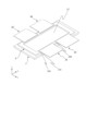
- FIG. 1 is a perspective view of an electronic component storage package and an electronic module according to an embodiment
- 2 is a see-through view of a lid of the electronic component storage package and the electronic module shown in FIG. 1 .
- FIG. 2 is a plan view of the electronic component storage package shown in FIG. 1 .
- 4 is a cross-sectional view of the electronic component storage package shown in FIG. 3 taken along line IV-IV.
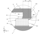
- FIG. 5 is an enlarged view of a main part A shown in FIG. 4 .
- 6 is a cross-sectional view of the electronic component storage package shown in FIG. 3 taken along line VI-VI.
- FIG. 7 is an enlarged view of a main part B shown in FIG. 6 .
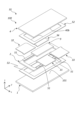
- FIG. 1 is a perspective view of an electronic component storage package according to one embodiment with a lid removed; 1 is an exploded perspective view of an electronic component storage package and an electronic module according to an embodiment; FIG. 13 is a perspective view of an electronic component storage package and an electronic module according to another embodiment.
- a conventional mounting structure includes a heat dissipation substrate, a ceramic frame body provided on the heat dissipation substrate and bonded via a thermosetting resin, a connection terminal provided on the ceramic frame body for electrically connecting the inside and outside of the ceramic frame body, and a lid body provided on the ceramic frame body.
- the connection terminal will fall off when stress is applied from below (the heat dissipation substrate side).
- ⁇ Configuration of Electronic Component Storage Package> ⁇ Configuration of Electronic Component Storage Package>
- any direction of the electronic component storage package may be regarded as up or down, for convenience, a Cartesian coordinate system xyz is defined, and the positive side of the z direction is regarded as up.
- a plan view is a concept that includes a planar perspective view.
- the package 100 for storing electronic components comprises a base body 1, a frame body 2, a conductive first connecting member 31, and a lid body 4.
- the base 1 has a first region 101.
- the base 1 has, for example, a rectangular shape in a plan view with dimensions of 5 mm ⁇ 10 mm to 25 mm ⁇ 50 mm and a thickness of 0.5 mm to 20 mm.
- An electronic component 9 (described later) can be positioned directly or indirectly on the first region 101 .
- the material of the substrate 1 may be, for example, a metal material such as copper, iron, tungsten, molybdenum, nickel, or cobalt, or an alloy containing these metal materials.
- the substrate 1 may be a single metal plate or a laminate of multiple metal plates. If the metal material constituting the substrate 1 is one of the above metal materials, a plating layer of nickel, gold, or the like may be formed on the surface of the substrate 1 by electroplating or electroless plating in order to reduce oxidation corrosion.
- the substrate 1 being made of a metal material here means that it is substantially made of a metal material, and may, for example, include a non-metallic material that is unavoidable in the manufacturing process.
- the material of the base 1 is an insulating material, and may be, for example, an aluminum oxide sintered body, a mullite sintered body, a silicon carbide sintered body, an aluminum nitride sintered body, a silicon nitride sintered body, or a ceramic material such as glass ceramics.
- the Young's modulus of the base 1 may be, for example, not less than 100 GPa and not more than 500 GPa.
- the frame body 2 is located on the base body 1 and surrounds the first region 101.
- the frame body 2 has a first frame body side surface 21s that intersects with the first connecting member 31 in a plan view.
- the surface that intersects with the first connecting member 31 can be defined as the first frame body side surface 21s.
- the material of the frame 2 may be, for example, a ceramic material such as an aluminum oxide sintered body, a mullite sintered body, a silicon carbide sintered body, an aluminum nitride sintered body, or a silicon nitride sintered body, or a dielectric material such as a glass ceramic material or a glass epoxy material.
- the surface of the frame 2 may be plated with a metal such as nickel or gold.
- metal wiring may be located on the inner layer and surface of the frame 2 .
- the frame body 2 does not necessarily have to be integrally molded.
- the frame body 2 may be formed by joining two U-shaped members, or may be formed into the shape of the frame body 2 by joining a plurality of members.
- a portion of the first connection member 31 is located on the frame body 2.
- the first connection member 31 extends outward in the first direction (i.e., the x-direction). In other words, the first connection member 31 protrudes outward from above the frame body 2. In this disclosure, outward refers to the direction away from the first region 101.
- a first bonding material 51 which will be described later, may be located between the first connection member 31 and the frame body 2.
- the dimension in the y direction of a part of the first connecting member 31 located on the frame body 2 may be larger than the dimension in the y direction of a part protruding from the frame body 2.
- the first connecting member 31 may be wider at the portion overlapping with the frame body 2.
- the material of the first connection member 31 include conductive materials such as iron-nickel alloy, iron-nickel-cobalt alloy, and copper. Metal plating may be present on the surface of the first connection member 31.
- the second connection member 32, third connection member 33, and fourth connection member 34 described below may also be made of the same or similar material as the first connection member 31.
- the first connection member 31 is a lead terminal, but is not limited to this, and the first connection member 31 may be, for example, a flexible printed circuit (FPC). Furthermore, a flexible circuit or a printed circuit board (PCB) on which an electronic circuit is formed may be connected to the tip of the first connection member 31. In other words, the first connection member 31 serves to electrically connect the inside and outside of the electronic component storage package 100.
- FPC flexible printed circuit
- PCB printed circuit board
- the lid body 4 is located on the first connection member 31.
- the material of the lid body 4 may be a ceramic material such as an aluminum oxide sintered body, a mullite sintered body, a silicon carbide sintered body, an aluminum nitride sintered body, or a silicon nitride sintered body, a dielectric material such as a glass ceramic material or a glass epoxy material, or a metal material such as copper, iron, tungsten, molybdenum, nickel, or cobalt, or an alloy containing these metal materials.
- the material of the lid body 4 may be the same as that of the frame body 2. In this case, it is possible to reduce the possibility that the lid body 4 and/or the frame body 2 will warp due to the difference in thermal expansion coefficient, and that the electronic component housing package 100 will be damaged.
- the lid body 4 and the frame body 2 are made of the same dielectric material, by making the combined thickness of the lid body 4 and the frame body 2 (the dimension in the z direction in the drawings) larger than the thickness of the base body 1, it is possible to reduce the possibility of the frame body 2 deforming due to the difference in thermal expansion coefficients even if the thermal expansion coefficient of the base body 1 is larger than that of the frame body 2. This reduces the possibility of the frame body 2 being damaged.
- the lid 4 has a first lid side 41s that intersects with the first connecting member 31 in a plan view.
- the first frame side 21s is located inward from the first lid side 41s.
- the first lid side 41s protrudes outward from the first frame side 21s.
- the inward direction refers to the opposite direction to the outward direction described above.
- the inward direction refers to the direction approaching the first region 101.
- the base 1 has a first base side surface 11s that intersects with the first connection member 31 in a plan view.
- the first frame side surface 21s may be located inward from the first base side surface 11s.
- the first base side surface 11s may protrude outward from the first frame side surface 21s.
- the distance L1 in the x direction between the first frame side surface 21s and the first base side surface 11s may be greater than the distance L2 in the x direction between the first frame side surface 21s and the first lid side surface 41s.
- the amount of protrusion L1 of the base 1 in the x direction relative to the frame 2 is greater than the amount of protrusion L2 of the lid 4 in the x direction relative to the frame 2.
- This configuration allows the lid 4 to be made smaller, so that the electronic component storage package 100 can be made smaller overall.
- the distance L1 in the x direction between the first frame side surface 21s and the first base side surface 11s may be greater than the distance L2 in the x direction between the first frame side surface 21s and the first lid side surface 41s.
- the base 1 can be seen in a plan view, so that the electronic component storage package 100 and the electronic module 10 can be easily arranged on other members.
- the first connection member 31 may bend upward, with the point where the first connection member 31 and the first lid side surface 41s intersect as a fulcrum.
- the above-described configuration reduces the possibility of an obstacle coming into contact with the first connection member 31 from below.
- the area near the fulcrum is covered by the base 1, so the first connection member 31 can be protected by the base 1.
- the distance L2 in the x direction between the first frame side surface 21s and the first lid side surface 41s may be greater than half the distance L1 in the x direction between the first frame side surface 21s and the first base side surface 11s.
- the distance L1 in the x direction between the first frame side surface 21s and the first base side surface 11s is, for example, 0.1 mm to 1.0 mm.
- the distance L2 in the x direction between the first frame side surface 21s and the first lid side surface 41s is, for example, 0.05 mm to 0.5 mm.
- the lid body 4 may have a lower surface 40b and a recess 40.
- the lower surface 40b faces the frame body 2.
- the recess 40 may be located on the lower surface 40b and overlap with the first region 101 in a planar view.
- the recess 40 also has a first inner wall surface 40s.
- the distance L3 between the first inner wall surface 40s and the first frame body side surface 21s may be greater than the distance L2 in the x direction between the first frame body side surface 21s and the first lid body side surface 41s.
- the dimension L3 in the x direction of the portion where the lid body 4 and the frame body 2 overlap may be greater than the protrusion amount L2 of the lid body 4 in the x direction relative to the frame body 2.
- the lid body 4 can be stably positioned on the frame body 2.
- the first inner wall surface 40s is the surface that connects with the lower surface 40b.
- the first inner wall surface 40s may be defined as a surface that faces the first lid side surface 41s, the second lid side surface 42s, the third lid side surface 43s, and the fourth lid side surface 44s in a cross-sectional view.
- the distance L3 between the first inner wall surface 40s and the first frame side surface 21s is, for example, 0.1 mm to 1.5 mm.
- the entire first lid side surface 41s may intersect with the first connecting member 31.
- the entire first connecting member 31 is covered by the lid body 4 in the y direction, so that the first connecting member 31 can be more stably positioned between the lid body 4 and the frame body 2. It is not necessary that all of the side surfaces of the lid body 4 protrude outward in the x direction from the first frame body side surface 21s of the frame body 2.
- a first lid body side surface 41s that intersects with the first connection member 31 may protrude in a plan view.
- the electronic component storage package 100 may further include a conductive second connection member 32, a part of which is located on the frame body 2, facing the first connection member 31 in the x direction and extending outward.
- the frame body 2 may have a second frame body side surface 22s that intersects with the second connection member 32 in a plan view.
- the lid body 4 may have a second lid body side surface 42s that intersects with the second connection member 32 in a plan view.
- the second frame body side surface 22s may be located inward from the second lid body side surface 42s.
- the above configuration can be rephrased as the dimension of the lid body 4 in the x direction being larger than the dimension of the frame body 2 in the x direction.
- the second connection member 32 can be stably positioned between the lid body 4 and the frame body 2.
- a distance L4 in the x direction between the second frame side surface 22s and the second base side surface 12s may be greater than or equal to a distance L5 in the x direction between the second frame side surface 22s and the second cover side surface 42s.
- a distance L5 in the x direction between the second frame side surface 22s and the second cover side surface 42s may be greater than half the distance L4 in the x direction between the second frame side surface 22s and the second base side surface 12s.
- the distance L6 between the first inner wall surface 40s and the second frame side surface 22s may be greater than the distance L5 in the x direction between the second frame side surface 22s and the second lid side surface 42s.
- the electronic component storage package 100 may further include a conductive third connection member 33 and a conductive fourth connection member 34, portions of which are located on the frame body 2.
- the third connection member 33 is located alongside the first connection member 31 in the y direction and extends outward in the x direction.
- the fourth connection member 34 is located alongside the second connection member 32 in the y direction and extends outward in the x direction.
- the fourth connection member 34 may also face the third connection member 33 in the x direction.
- the frame 2 may have a third frame side surface 23s that intersects with the third connecting member 33 in a plan view.
- the lid 4 may have a third lid side surface 43s that intersects with the third connecting member 33 in a plan view. In this case, the third frame side surface 23s may be located inward of the third lid side surface 43s.
- the frame 2 may have a fourth frame side surface 24s that intersects with the fourth connecting member 34 in a plan view.
- the lid 4 may have a fourth lid side surface 44s that intersects with the fourth connecting member 34 in a plan view. In this case, the fourth frame side surface 24s may be located inward from the fourth lid side surface 44s.
- the third frame side surface 23s may be flush with the first frame side surface 21s, and the fourth frame side surface 24s may be flush with the second frame side surface 22s.
- the third lid side surface 43s may be flush with the first lid side surface 41s, and the fourth lid side surface 44s may be flush with the second lid side surface 42s.
- the base 1 may have a second base side surface 12s that intersects with the second connecting member 32 in a plan view.
- the second frame side surface 22s may be located inward from the second base side surface 12s.
- the dimension of the base 1 in the x direction may be greater than the dimension of the frame 2 in the x direction.
- the package 100 for storing electronic components only needs to have the dimension of the lid body 4 in the x direction on the long side (the direction along the y direction in the drawings) greater than the dimension of the frame body 2 in the x direction. Also, the package 100 for storing electronic components may have the dimension of the lid body 4 in the y direction on the short side (the direction along the x direction in the drawings) the same as the dimension of the frame body 2 in the y direction.
- the electronic component storage package 100 may have the side surface of the frame 2 and the side surface of the lid 4 flush with each other on the short side (the direction along the x direction in the drawings). In this case, it is easy to align the lid 4 with the frame 2 using the flush side surfaces of the frame 2 and the lid 4 as a reference.
- the base 1 may have a third base side surface 13s that intersects with the third connection member 33 in a plan view.
- the third frame side surface 23s may be located inward from the third base side surface 13s.
- the base 1 may have a fourth base side surface 14s that intersects with the fourth connecting member 34 in a plan view.
- the fourth frame side surface 24s may be located inward from the fourth base side surface 14s.
- the third substrate side surface 13s may be flush with the first substrate side surface 11s, and the fourth substrate side surface 14s may be flush with the second substrate side surface 12s.
- the electronic component storage package 100 may further include a first bonding material 51 and a second bonding material 52.
- the first bonding material 51 is located between the frame body 2 and the first connecting member 31, and may contain a first resin material.
- the material of the first bonding material 51 may be, for example, a brazing material or solder.
- the first bonding material 51 contains the first resin material, the temperature during bonding between the frame body 2 and the first connecting member 31 can be lowered compared to when the first bonding material 51 is a brazing material or solder. Therefore, the possibility that the first connecting member 31 and/or the frame body 2 will be warped or deteriorated due to heat during bonding can be reduced.
- the first resin material may be, for example, a thermoplastic resin such as an epoxy resin, a polyimide resin, or a silicone resin.
- the first bonding material 51 may also contain an inorganic filler in addition to the first resin material.
- inorganic filler materials include silica glass fiber, alumina fiber, carbon fiber, barium sulfate, and titanium oxide.
- the first bonding material 51 may form a fillet from the back surface (the surface facing the frame body 2) of the first connection member 31 to the first frame body side surface 21s. This configuration can improve the bonding strength between the first connection member 31 and the frame body 2. More specifically, the first bonding material 51 may have a convex shape on the inside and outside in a cross-sectional view.
- the heat resistance temperature of the first bonding material 51 may be higher than the heat resistance temperature of the second bonding material 52 described below.
- the first connection member 31 is electrically connected to the electronic component 9 described below, for example, by a bonding wire.
- the bonding wire is connected to the first connection member 31, heat is applied.
- the above-described configuration reduces the possibility that the first bonding material 51 will deteriorate or break when wire bonding to the first connection member 31. Therefore, when wire bonding to the first connection member 31, the possibility that the first connection member 31 will shift or fall off from the frame body 2 can be reduced.
- the second bonding material 52 may be located between the lid body 4 and the frame body 2 and may contain a second resin material.
- the second bonding material 52 may also be located between the lid body 4 and the first connecting member 31. In other words, the second bonding material 52 is in contact with each of the lid body 4, the frame body 2, and the first connecting member 31.
- the second resin material may be a so-called B-stage epoxy material.
- the second bonding material 52 is applied in advance to the lower surface 40b of the lid body 4 and the first recessed portion 401 described below to be in a B-stage state (semi-cured state), and after the electronic component 9 is positioned on the first region 101, the lid body 4 to which the second bonding material 52 has been applied is positioned on the frame body 2 and/or the first connecting member 31, and the second bonding material 52 is then cured to stably bond the lid body 4 and the frame body 2.
- the lid 4 may have a bottom surface 40b and a recess 40.
- the bottom surface 40b faces the frame 2.
- the recess 40 is located on the bottom surface 40b and overlaps with the first region 101 in a plan view.
- the recess 40 has a first inner wall surface 40s.
- the second bonding material 52 may be in contact with the first inner wall surface 40s and the first frame side surface 21s. This configuration can improve the bonding strength between the lid 4 and the frame 2. This can improve the airtightness of the electronic component storage package 100.
- the second bonding material 52 may form a fillet from the lower surface 40b to the first frame side surface 21s.
- the second bonding material 52 may also form a fillet from the upper surface of the frame 2 to the first inner wall surface 40s.
- the second bonding material 52 may be convex inward and outward in a cross-sectional view. In this case, the point where the first connecting member 31 intersects with the first cover side surface 41s and the point where the first connecting member 31 intersects with the inner wall surface 40s can be protected from external obstacles.
- stress is applied to the first connecting member 31, the possibility that the first connecting member 31 will be deformed can be reduced by using the point where the first connecting member 31 intersects with the first cover side surface 41s as a fulcrum.
- the second bonding material 52 may be in contact with the first lid side surface 41s. This configuration can further improve the bonding strength between the lid 4 and the frame 2. In addition, since the bonding strength between the lid 4 and the frame 2 is improved, the airtightness of the electronic component storage package 100 can be improved.
- the second bonding material 52 may form a fillet from the top surface of the first connection member 31 (the surface facing the lid body 4) to the first lid body side surface 41s. This configuration can improve the bonding strength between the lid body 4 and the first connection member 31.
- the lid body 4 may have a first recessed portion 401 recessed along the first connecting member 31 in the y direction.
- the first recessed portion 401 may overlap the first connecting member 31 in a plan view.
- the thickness of the lid body 4 located on the first connecting member 31 can be reduced compared to when the first recessed portion 401 is not present (in other words, when the lower surface 40b is flush).
- the lid body 4 and the frame body 2 can be firmly bonded by the second bonding material 52. Therefore, the airtightness of the electronic component storage package 100 can be improved.
- the lid body 4 and the frame body 2 can be bonded.
- the first connecting member 31 is pressed by the first recessed portion 401, thereby reducing the possibility that the first connecting member 31 will be displaced, distorted, or dropped off.
- the first recessed portion 401 may be continuous with the recess 40.
- the cover 4 may further include a second recess 402, a third recess 403, and a fourth recess 404.
- the second recess 402 may be recessed in the y direction along the second connecting member 32.
- the third recess 403 may be recessed in the y direction along the third connecting member 33.
- the fourth recess 404 may be recessed in the y direction along the fourth connecting member 34.
- the frame 2 may contain a ceramic material.
- the base 1 may contain copper at a ratio of 95% by weight or more. In this case, the base 1 can be effectively used as a heat sink, and the heat generated by the electronic component 9 can be efficiently dissipated.
- the thermal expansion coefficient of the base 1 may be 1.5 to 3.0 times that of the frame 2 .
- the electronic component storage package 100 may further include a third bonding material 53.
- the third bonding material 53 is located between the base body 1 and the frame body 2, and contains a third resin material.
- the third bonding material 53 has excellent elasticity because it contains the third resin material. Therefore, even if the thermal expansion coefficient of the base body 1 is different from the thermal expansion coefficient of the frame body 2 (for example, the thermal expansion coefficient of the base body 1 is 1.5 to 3.0 times the thermal expansion coefficient of the frame body 2), the possibility that the frame body 2 will fall off the base body 1 or the frame body 2 will be damaged due to the difference in thermal expansion coefficients can be reduced.
- the third resin material may be the same as or different from the first resin material.
- the electronic module 10 according to the embodiment of the present disclosure further includes an electronic component storage package 100 and an electronic component 9 .
- the electronic component 9 may be a component that performs signal processing, such as converting a radio signal or an optical signal into an electrical signal, or converting an electrical signal into an optical signal or a radio signal.
- the electronic component 9 is located on the first region 101 and is housed in the electronic component housing package 100.
- the electronic component 9 is electrically connected to the first connection member 31 via a conductive member such as a bonding wire.
- the electronic component 9 may also be electrically connected to the second connection member 32 to the fourth connection member 34.
- the number of electronic components 9 located on the first region 101 is not necessarily limited to one, and there may be a plurality of electronic components 9 .
- the electronic component 9 can be formed from a semiconductor material such as gallium arsenide or gallium nitride. More specifically, the electronic component 9 can be a so-called power semiconductor element that uses a wide band gap semiconductor.
- the electronic component 9 may also be, for example, an optical semiconductor element such as a semiconductor laser (LD: Laser Diode) or a photodiode (PD: Photodiode), a semiconductor integrated circuit element such as a field effect transistor (FET: Field Effect Transistor), or a sensor element such as an optical sensor.
- an optical semiconductor element such as a semiconductor laser (LD: Laser Diode) or a photodiode (PD: Photodiode), a semiconductor integrated circuit element such as a field effect transistor (FET: Field Effect Transistor), or a sensor element such as an optical sensor.
- the electronic component 9 does not necessarily have to be located directly on the first region 101, but may be located indirectly on the first region 101 via a so-called submount.
- This disclosure can be used as a package for storing electronic components and an electronic module.
Landscapes
- Piezo-Electric Or Mechanical Vibrators, Or Delay Or Filter Circuits (AREA)
Priority Applications (1)
| Application Number | Priority Date | Filing Date | Title |
|---|---|---|---|
| JP2025516803A JPWO2024225235A1 (https=) | 2023-04-25 | 2024-04-23 |
Applications Claiming Priority (2)
| Application Number | Priority Date | Filing Date | Title |
|---|---|---|---|
| JP2023071665 | 2023-04-25 | ||
| JP2023-071665 | 2023-04-25 |
Publications (1)
| Publication Number | Publication Date |
|---|---|
| WO2024225235A1 true WO2024225235A1 (ja) | 2024-10-31 |
Family
ID=93256444
Family Applications (1)
| Application Number | Title | Priority Date | Filing Date |
|---|---|---|---|
| PCT/JP2024/015797 Ceased WO2024225235A1 (ja) | 2023-04-25 | 2024-04-23 | 電子部品収納用パッケージおよび電子モジュール |
Country Status (2)
| Country | Link |
|---|---|
| JP (1) | JPWO2024225235A1 (https=) |
| WO (1) | WO2024225235A1 (https=) |
Citations (2)
| Publication number | Priority date | Publication date | Assignee | Title |
|---|---|---|---|---|
| JPH02116740U (https=) * | 1989-03-03 | 1990-09-19 | ||
| WO2023054246A1 (ja) * | 2021-09-30 | 2023-04-06 | 京セラ株式会社 | 電子部品搭載用パッケージ及び電子装置 |
-
2024
- 2024-04-23 WO PCT/JP2024/015797 patent/WO2024225235A1/ja not_active Ceased
- 2024-04-23 JP JP2025516803A patent/JPWO2024225235A1/ja active Pending
Patent Citations (2)
| Publication number | Priority date | Publication date | Assignee | Title |
|---|---|---|---|---|
| JPH02116740U (https=) * | 1989-03-03 | 1990-09-19 | ||
| WO2023054246A1 (ja) * | 2021-09-30 | 2023-04-06 | 京セラ株式会社 | 電子部品搭載用パッケージ及び電子装置 |
Also Published As
| Publication number | Publication date |
|---|---|
| JPWO2024225235A1 (https=) | 2024-10-31 |
Similar Documents
| Publication | Publication Date | Title |
|---|---|---|
| CN100562999C (zh) | 电路模块 | |
| CN101901795A (zh) | 功率半导体模块 | |
| CN104126224B (zh) | 元件收纳用封装件 | |
| KR102490612B1 (ko) | 전력용 반도체 모듈 | |
| JPWO2018151176A1 (ja) | 熱電素子内蔵パッケージ | |
| CN110140205B (zh) | 半导体装置 | |
| KR102829692B1 (ko) | 파워모듈 및 그 제조방법 | |
| JP2000340876A (ja) | 光半導体素子用パッケージおよびその製造方法 | |
| US20240321692A1 (en) | Power module | |
| US20250202189A1 (en) | Tube-housing packaging member, packaging assembly, and lidar transmit module | |
| JP2022173218A (ja) | 発光素子搭載用基板および発光装置 | |
| KR102792456B1 (ko) | 파워모듈 및 그 제조방법 | |
| JP4822820B2 (ja) | 半導体素子収納用パッケージおよび半導体装置 | |
| JP6626735B2 (ja) | 電子部品搭載用基板、電子装置および電子モジュール | |
| WO2024225235A1 (ja) | 電子部品収納用パッケージおよび電子モジュール | |
| KR20210141903A (ko) | 파워모듈 | |
| US20040173898A1 (en) | Semiconductor apparatus having system-in-package arrangement with improved heat dissipation | |
| WO2023089059A2 (en) | Laser package and method for manufacturing a laser package | |
| JPH09330994A (ja) | 半導体装置 | |
| KR20230136459A (ko) | 전력 반도체 모듈 및 전력 반도체 모듈의 제조 방법 | |
| JP4360577B2 (ja) | 半導体装置 | |
| US20250006565A1 (en) | Electronic component housing package and electronic module | |
| JP2007012718A (ja) | 電子部品収納用パッケージおよび電子装置 | |
| CN222749495U (zh) | 一种轻薄型的集成电路框架和半导体器件 | |
| JP7196249B2 (ja) | 半導体素子用パッケージおよび半導体装置 |
Legal Events
| Date | Code | Title | Description |
|---|---|---|---|
| 121 | Ep: the epo has been informed by wipo that ep was designated in this application |
Ref document number: 24796981 Country of ref document: EP Kind code of ref document: A1 |
|
| ENP | Entry into the national phase |
Ref document number: 2025516803 Country of ref document: JP Kind code of ref document: A |
|
| WWE | Wipo information: entry into national phase |
Ref document number: 2025516803 Country of ref document: JP |
|
| NENP | Non-entry into the national phase |
Ref country code: DE |
|
| 122 | Ep: pct application non-entry in european phase |
Ref document number: 24796981 Country of ref document: EP Kind code of ref document: A1 |