WO2024224711A1 - 積層セラミックコンデンサ - Google Patents
積層セラミックコンデンサ Download PDFInfo
- Publication number
- WO2024224711A1 WO2024224711A1 PCT/JP2024/001186 JP2024001186W WO2024224711A1 WO 2024224711 A1 WO2024224711 A1 WO 2024224711A1 JP 2024001186 W JP2024001186 W JP 2024001186W WO 2024224711 A1 WO2024224711 A1 WO 2024224711A1
- Authority
- WO
- WIPO (PCT)
- Prior art keywords
- laminate
- thin film
- film layer
- main surface
- layer
- Prior art date
- Legal status (The legal status is an assumption and is not a legal conclusion. Google has not performed a legal analysis and makes no representation as to the accuracy of the status listed.)
- Ceased
Links
Images









Classifications
-
- H—ELECTRICITY
- H01—ELECTRIC ELEMENTS
- H01G—CAPACITORS; CAPACITORS, RECTIFIERS, DETECTORS, SWITCHING DEVICES, LIGHT-SENSITIVE OR TEMPERATURE-SENSITIVE DEVICES OF THE ELECTROLYTIC TYPE
- H01G4/00—Fixed capacitors; Processes of their manufacture
- H01G4/30—Stacked capacitors
-
- H—ELECTRICITY
- H01—ELECTRIC ELEMENTS
- H01G—CAPACITORS; CAPACITORS, RECTIFIERS, DETECTORS, SWITCHING DEVICES, LIGHT-SENSITIVE OR TEMPERATURE-SENSITIVE DEVICES OF THE ELECTROLYTIC TYPE
- H01G4/00—Fixed capacitors; Processes of their manufacture
- H01G4/002—Details
- H01G4/005—Electrodes
- H01G4/012—Form of non-self-supporting electrodes
-
- H—ELECTRICITY
- H01—ELECTRIC ELEMENTS
- H01G—CAPACITORS; CAPACITORS, RECTIFIERS, DETECTORS, SWITCHING DEVICES, LIGHT-SENSITIVE OR TEMPERATURE-SENSITIVE DEVICES OF THE ELECTROLYTIC TYPE
- H01G4/00—Fixed capacitors; Processes of their manufacture
- H01G4/002—Details
- H01G4/018—Dielectrics
- H01G4/06—Solid dielectrics
- H01G4/08—Inorganic dielectrics
- H01G4/12—Ceramic dielectrics
-
- H—ELECTRICITY
- H01—ELECTRIC ELEMENTS
- H01G—CAPACITORS; CAPACITORS, RECTIFIERS, DETECTORS, SWITCHING DEVICES, LIGHT-SENSITIVE OR TEMPERATURE-SENSITIVE DEVICES OF THE ELECTROLYTIC TYPE
- H01G4/00—Fixed capacitors; Processes of their manufacture
- H01G4/002—Details
- H01G4/228—Terminals
- H01G4/232—Terminals electrically connecting two or more layers of a stacked or rolled capacitor
-
- H—ELECTRICITY
- H01—ELECTRIC ELEMENTS
- H01G—CAPACITORS; CAPACITORS, RECTIFIERS, DETECTORS, SWITCHING DEVICES, LIGHT-SENSITIVE OR TEMPERATURE-SENSITIVE DEVICES OF THE ELECTROLYTIC TYPE
- H01G4/00—Fixed capacitors; Processes of their manufacture
- H01G4/002—Details
- H01G4/228—Terminals
- H01G4/232—Terminals electrically connecting two or more layers of a stacked or rolled capacitor
- H01G4/2325—Terminals electrically connecting two or more layers of a stacked or rolled capacitor characterised by the material of the terminals
Definitions
- the present invention relates to a multilayer ceramic capacitor.
- a multilayer ceramic capacitor is known in which the dimension T in the Z-axis direction (stacking direction) is less than 0.3 mm.
- the multilayer ceramic capacitor described in Patent Document 1 has external electrodes that are composed of a base film made of a sintered metal film and a plating film placed on top of that.
- the main objective of the present invention is to provide a multilayer ceramic capacitor that can distribute the stress applied to the ends of the thin film layer (base film) and suppress the propagation of cracks into the interior of the multilayer ceramic capacitor.
- the multilayer ceramic capacitor of the present invention comprises a laminate including a plurality of laminated dielectric layers, a first main surface and a second main surface facing each other in the lamination direction, a first side surface and a second side surface facing each other in a width direction perpendicular to the lamination direction, a first end surface and a second end surface facing each other in a length direction perpendicular to the lamination direction and the width direction, a first internal electrode layer alternately laminated with the plurality of dielectric layers and exposed at the first end surface, and a second internal electrode layer alternately laminated with the plurality of dielectric layers and exposed at the second end surface, and a conductive layer covering a portion of the first end surface and a portion of the first main surface of the laminate.
- the laminated ceramic capacitor has a first external electrode arranged so as to cover a portion of the second end face and a portion of the first main surface of the laminate, and each of the first external electrode and the second external electrode has a thin film layer covering at least a portion of the first main surface, an underplating layer covering at least a portion of the thin film layer, an upper plating layer arranged on the underplating layer, and a top plating layer arranged on the upper plating layer, and on the first main surface, an edge portion of the thin film layer located toward the center of the laminate is separated from the laminate.
- the multilayer ceramic capacitor according to the present invention also comprises a laminate including a plurality of laminated dielectric layers, a first main surface and a second main surface facing each other in the lamination direction, a first side surface and a second side surface facing each other in a width direction perpendicular to the lamination direction, a third side surface and a fourth side surface facing each other in a length direction perpendicular to the lamination direction and the width direction, a first internal electrode layer alternately laminated with the plurality of dielectric layers and exposed at least on the first side surface and the second side surface, and a second internal electrode layer alternately laminated with the plurality of dielectric layers and exposed at least on the first side surface and the second side surface, a first external electrode arranged to cover a portion of the first side surface and a portion of the first main surface of the laminate, and a second external electrode arranged to cover a portion of the second side surface and a portion of the first main surface of the laminate.
- each of the first external electrode, the second external electrode, the third external electrode, and the fourth external electrode includes a thin film layer covering at least a portion of one or more surfaces of the laminate, an underplating layer covering at least a portion of the thin film layer, an upper plating layer arranged on the underplating layer, and a top plating layer arranged on the upper plating layer, and an edge portion of the thin film layer located on the center side of the laminate is separated from the laminate.
- the edge portion located at the center of the laminate of the thin film layers is spaced from the laminate, dispersing the stress acting on the edge portion of the thin film layers and suppressing the propagation of cracks into the interior of the multilayer ceramic capacitor.
- the present invention provides a multilayer ceramic capacitor that can distribute the stress applied to the ends (edges) of the thin film layer (base film) and suppress the propagation of cracks into the interior of the multilayer ceramic capacitor.
- FIG. 1 is an external perspective view showing a multilayer ceramic capacitor according to a first embodiment of the present invention
- 1 is a front view showing a multilayer ceramic capacitor according to a first embodiment of the present invention
- 1 is a top view showing a multilayer ceramic capacitor according to a first embodiment of the present invention
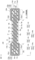
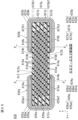
- FIG. 4 is a cross-sectional view taken along line IV-IV in FIG. 2 is a cross-sectional view taken along line VV in FIG. 1.
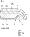
- FIG. 5 is an enlarged view of a portion ⁇ in FIG. 4 .
- FIG. 5 is an external perspective view showing a multilayer ceramic capacitor according to a second embodiment of the present invention.
- FIG. 4 is a front view showing a multilayer ceramic capacitor according to a second embodiment of the present invention.
- FIG. 4 is a top view showing a multilayer ceramic capacitor according to a second embodiment of the present invention.
- 8 is a cross-sectional view taken along line XX in FIG. 7.
- 8 is a cross-sectional view taken along line XI-XI in FIG. 7.
- FIG. 11 is an external perspective view showing a multilayer ceramic capacitor according to a third embodiment of the present invention.
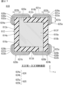
- 13 is a cross-sectional view taken along line XIII-XIII in FIG. 12.
- 13 is a cross-sectional view taken along line XIV-XIV in FIG. 12.
- 13 is a cross-sectional view taken along line XV-XV in FIG. 12.
- FIG. 11 is a top view showing a laminate and a thin film layer of a multilayer ceramic capacitor according to a third embodiment of the present invention.
- FIG. 11 is a bottom view showing a laminate and a thin film layer of a multilayer ceramic capacitor according to a third embodiment of the present invention.
- FIG. 11 is a front view showing a laminate and a thin film layer of a multilayer ceramic capacitor according to a third embodiment of the present invention.
- FIG. 11 is a rear view showing a laminate and a thin film layer of the multilayer ceramic capacitor according to the third embodiment of the present invention.
- FIG. 11 is a left side view showing a laminate and a thin film layer of a multilayer ceramic capacitor according to a third embodiment of the present invention.
- FIG. 11 is a top view showing a laminate and a thin film layer of a multilayer ceramic capacitor according to a third embodiment of the present invention.
- FIG. 11 is a bottom view showing a laminate and a thin film layer of a multilayer ceramic capacitor according to
- FIG. 11 is a right side view showing a laminate and a thin film layer of a multilayer ceramic capacitor according to a third embodiment of the present invention.
- FIG. 14 is an enlarged view of the ⁇ portion in FIG. 13 .
- FIG. 13 is an exploded perspective view of the laminate shown in FIG. 12 .
- FIG. 13 is an external perspective view showing a multilayer ceramic capacitor according to a fourth embodiment of the present invention.
- 25 is a cross-sectional view taken along line XXV-XXV in FIG. 24. 25 is a cross-sectional view taken along line XXVI-XXVI in FIG. 24. 25 is a cross-sectional view taken along line XXVII-XXVII in FIG. 24.
- FIG. 25 is an exploded perspective view of the laminate shown in FIG.
- FIG. 13 is an external perspective view showing a multilayer ceramic capacitor according to a fifth embodiment of the present invention.
- FIG. 13 is a bottom view showing a multilayer ceramic capacitor according to a fifth embodiment of the present invention.
- 30 is a cross-sectional view taken along line XXXI-XXXI in FIG. 29.
- 30 is a cross-sectional view taken along line XXXII-XXXII in FIG. 29.
- the multilayer ceramic capacitor according to the present invention will be described below.
- FIG. 1 is an external perspective view showing the multilayer ceramic capacitor according to the first embodiment of the present invention.
- FIG. 2 is a front view showing the multilayer ceramic capacitor according to the first embodiment of the present invention.
- FIG. 3 is a top view showing the multilayer ceramic capacitor according to the first embodiment of the present invention.
- FIG. 4 is a cross-sectional view taken along line IV-IV in FIG. 1.
- FIG. 5 is a cross-sectional view taken along line V-V in FIG. 1.
- FIG. 6 is an enlarged view of the ⁇ portion in FIG. 4.
- the multilayer ceramic capacitor 10 has a laminate 12 and an external electrode 24. Below, the configuration of each component will be explained in the order of the laminate 12 and the external electrode 24.
- the laminate 12 includes a plurality of stacked dielectric layers 14 and a plurality of stacked internal electrode layers 16.
- the laminate 12 further includes a first main surface 12a and a second main surface 12b that face the stacking direction x, a first side surface 12c and a second side surface 12d that face the width direction y perpendicular to the stacking direction x, and a first end surface 12e and a second end surface 12f that face the length direction z perpendicular to the stacking direction x and the width direction y.
- the first main surface 12a and the second main surface 12b extend along the width direction y and the length direction z, respectively.
- the first side surface 12c and the second side surface 12d extend along the stacking direction x and the length direction z, respectively.
- the first end surface 12e and the second end surface 12f extend along the stacking direction x and the width direction y, respectively. Therefore, the stacking direction x is the direction connecting the first main surface 12a and the second main surface 12b, the width direction y is the direction connecting the first side surface 12c and the second side surface 12d, and the length direction z is the direction connecting the first end surface 12e and the second end surface 12f.
- the surfaces of the first main surface 12a and the second main surface 12b, the first side surface 12c and the second side surface 12d, and the first end surface 12e and the second end surface 12f may be provided with irregularities, or may be roughened.
- the corners and ridges of the laminate 12 are rounded. Note that a corner refers to a portion where three adjacent faces of the laminate 12 intersect, and a ridge refers to a portion where two adjacent faces of the laminate 12 intersect.
- the laminate 12 has an inner layer portion 15a in which multiple internal electrode layers 16 face each other in the stacking direction x connecting the first main surface 12a and the second main surface 12b, a first main surface side outer layer portion 15b1 formed from multiple dielectric layers 14 located between the internal electrode layer 16 located closest to the first main surface 12a and the first main surface 12a, and a second main surface side outer layer portion 15b2 formed from multiple dielectric layers 14 located between the internal electrode layer 16 located closest to the second main surface 12b and the second main surface 12b.
- the dielectric layer 14 has an inner dielectric layer 14a which is the dielectric layer 14 of the inner layer portion 15a, and an outer dielectric layer 14b which is the dielectric layer 14 of the first main surface side outer layer portion 15b1 and the second main surface side outer layer portion 15b2.
- the first main surface side outer layer portion 15b1 is located on the first main surface 12a side of the laminate 12, and is an assembly of multiple outer dielectric layers 14b located between the first main surface 12a and the internal electrode layer 16 closest to the first main surface 12a.
- the second main surface side outer layer portion 15b2 is located on the second main surface 12b side of the laminate 12, and is an assembly of multiple outer dielectric layers 14b located between the second main surface 12b and the internal electrode layer 16 closest to the second main surface 12b.
- the area sandwiched between the first main surface side outer layer portion 15b1 and the second main surface side outer layer portion 15b2 is the inner layer portion 15a.
- the inner layer portion 15a is the area where the internal electrode layers 16 are stacked.
- the inner layer portion 15a includes an inner dielectric layer 14a, a first internal electrode layer 16a alternately stacked with the inner dielectric layer 14a, and a second internal electrode layer 16b alternately stacked with the inner dielectric layer 14a.
- the first internal electrode layer 16a is exposed at the first end face 12e.
- the second internal electrode layer 16b is exposed at the second end face 12f.
- the dielectric layer 14 may have a plurality of crystal grains including a perovskite type compound having a basic structure of BaTiO 3 .
- the dielectric layer 14 may be formed from, for example, a dielectric material.
- the dielectric material may be, for example, a dielectric ceramic composed of a main component such as BaTiO3 , CaTiO3 , SrTiO3 , or CaZrO3 .
- a material containing a subcomponent such as a Mn compound, an Fe compound, a Cr compound, a Co compound, or a Ni compound added to the main component may also be used.
- the inner dielectric layer 14a and the outer dielectric layer 14b may be used for different materials, taking into consideration the required functions.
- the outer dielectric layer 14b is made of a soft material, it is possible to buffer the stress on the laminate 12.
- the outer dielectric layer 14b is made of a hard material, it is possible to suppress the occurrence of cracks.
- the first main surface side outer layer portion 15b1 and the second main surface side outer layer portion 15b2 are each an assembly of multiple outer dielectric layers 14b.
- the first main surface side outer layer portion 15b1 and the second main surface side outer layer portion 15b2 may become integrated after baking and may not be distinguished from each other.
- the number of dielectric layers 14 to be stacked is not particularly limited, but it is preferable that the number be 30 or more and 90 or less, including the outer dielectric layer 14b. In addition, it is preferable that the thickness of the dielectric layer 14 is 0.5 ⁇ m or less.
- the internal electrode layer 16 has a first internal electrode layer 16a and a second internal electrode layer 16b.
- the first internal electrode layer 16a is alternately stacked with a plurality of dielectric layers 14 and is exposed at the first end face 12e.
- the second internal electrode layer 16b is alternately stacked with a plurality of dielectric layers 14 and is exposed at the second end face 12f.
- the first internal electrode layer 16a and the second internal electrode layer 16b are alternately stacked with the inner dielectric layer 14a interposed therebetween.
- the first internal electrode layer 16a is disposed on the surface of the inner dielectric layer 14a.
- the first internal electrode layer 16a has a first opposing electrode portion 18a that faces the second internal electrode layer 16b, and a first lead electrode portion 20a that is located on one end side of the first internal electrode layer 16a and extends from the first opposing electrode portion 18a to the first end face 12e of the laminate 12. The end of the first lead electrode portion 20a is led out to the first end face 12e and exposed.
- the shape of the first opposing electrode portion 18a of the first internal electrode layer 16a is not particularly limited, but is preferably rectangular in plan view. However, the corners in plan view may be rounded or may be formed at an angle in plan view (tapered). It may also be tapered in plan view, with a slope in either direction.
- the shape of the first extraction electrode portion 20a of the first internal electrode layer 16a is not particularly limited, but is preferably rectangular in plan view. However, the corners in plan view may be rounded or may be formed at an angle in plan view (tapered). It may also be tapered in plan view, with a slope in either direction.
- the width of the first extraction electrode portion 20a may be tapered, narrowing from the first opposing electrode portion 18a toward the first end face 12e.
- the width in the width direction y of the first extraction electrode portion 20a may be narrower than the width of the first opposing electrode portion 18a.
- the width of the first extraction electrode portion 20a may be formed to be the same as the width of the first opposing electrode portion 18a.
- the second internal electrode layer 16b is disposed on a surface of an inner dielectric layer 14a different from the inner dielectric layer 14a on which the first internal electrode layer 16a is disposed.
- the second internal electrode layer 16b has a second opposing electrode portion 18b that faces the first internal electrode layer 16a, and a second extraction electrode portion 20b that is located on one end side of the second internal electrode layer 16b and extends from the second opposing electrode portion 18b to the second end face 12f of the laminate 12.
- the end of the second extraction electrode portion 20b is extended to the second end face 12f and exposed.
- the shape of the second opposing electrode portion 18b of the second internal electrode layer 16b is not particularly limited, but is preferably rectangular in plan view. However, the corners in plan view may be rounded or may be formed at an angle in plan view (tapered). It may also be tapered in plan view, with a slope in either direction.
- the shape of the second extraction electrode portion 20b of the second internal electrode layer 16b is not particularly limited, but is preferably rectangular in plan view. However, the corners in plan view may be rounded or may be formed at an angle in plan view (tapered). It may also be tapered in plan view, with a slope in either direction.
- the width of the second extraction electrode portion 20b may be tapered, narrowing from the second opposing electrode portion 18b toward the second end face 12f.
- the width in the width direction y of the second extraction electrode portion 20b may be narrower than the width of the second opposing electrode portion 18b.
- the width of the second extraction electrode portion 20b may be formed to be the same as the width of the second opposing electrode portion 18b.
- the first and second lead-out electrode portions 20a and 20b may be curved toward the first main surface 12a or the second main surface 12b. Furthermore, the longest distance in the stacking direction x between the exposed portion of the first internal electrode layer 16a and the exposed portion of the second internal electrode layer 16b that are led out to the first end face 12e or the second end face 12f may be shorter than the longest distance in the stacking direction x between the first opposing electrode portion 18a of the first internal electrode layer 16a and the second opposing electrode portion 18b of the second internal electrode layer 16b.
- Capacitance is generated when the first internal electrode layer 16a and the second internal electrode layer 16b face each other via the inner dielectric layer 14a.
- the laminate 12 includes ends (hereinafter referred to as "L gaps") 22b of the laminate 12 formed between the end of the first internal electrode layer 16a opposite the first lead electrode portion 20a and the second end face 12f, and between the end of the second internal electrode layer 16b opposite the second lead electrode portion 20b and the first end face 12e.
- the laminate 12 includes a side portion (hereinafter referred to as a "W gap") 22a of the laminate 12 formed between one end of the first opposing electrode portion 18a and the second opposing electrode portion 18b in the width direction y and the first side surface 12c, and between the other end of the first opposing electrode portion 18a and the second opposing electrode portion 18b in the width direction y and the second side surface 12d.
- a W gap a side portion of the laminate 12 formed between one end of the first opposing electrode portion 18a and the second opposing electrode portion 18b in the width direction y and the first side surface 12c
- the first internal electrode layer 16a and the second internal electrode layer 16b can be made of an appropriate conductive material, such as a metal such as Ni, Cu, Ag, Pd, or Au, or an Ag-Pd alloy that contains one of these metals.
- the first internal electrode layer 16a and the second internal electrode layer 16b may contain Sn.
- Sn in the first internal electrode layer 16a and the second internal electrode layer 16b, the potential barrier height at the interface between the first internal electrode layer 16a and the second internal electrode layer 16b and the inner dielectric layer 14a can be increased, and the thickness of the depletion layer can be increased. This can alleviate electric field concentration at the interface, leading to improved high temperature load reliability.
- Sn can be sufficiently effective even if it is contained in only one of the internal electrode layers 16, the first internal electrode layer 16a or the second internal electrode layer 16b.
- the area of the internal electrode layer 16 must be increased.
- the LW surface coverage of the internal electrode layer 16 is 90% or more.
- the LW surface coverage is defined as the ratio of the area inside the edge of the internal electrode layer 16 when viewed from a cross section (LW surface) of the laminate 12 in the width direction y and length direction z, minus the area of the gap. The higher the LW surface coverage, the higher the capacitance of the capacitor, but even if it is low, the inner dielectric layers 14a are bonded together via gaps, so the bonding strength between the layers is high and delamination is less likely to occur.
- the thickness of the internal electrode layers 16, i.e., the first internal electrode layers 16a and the second internal electrode layers 16b, is preferably 0.3 ⁇ m or more and 0.9 ⁇ m or less.
- the total number of the first internal electrode layers 16a and the second internal electrode layers 16b is preferably 20 or more and 80 or less.
- the external electrode 24 has a first external electrode 24a and a second external electrode 24b.
- the first external electrode 24a is connected to the first internal electrode layer 16a and is arranged to cover a portion of the first end face 12e and a portion of the first main face 12a of the laminate 12. It may also extend slightly around a portion of the second main face 12b, a portion of the first side face 12c, and/or a portion of the second side face 12d.
- the second external electrode 24b is connected to the second internal electrode layer 16b and is arranged to cover a portion of the second end face 12f and a portion of the first main face 12a of the laminate 12. It may also extend slightly around a portion of the second main face 12b, a portion of the first side face 12c, and/or a portion of the second side face 12d.
- Each of the external electrodes 24, i.e., the first external electrode 24a and the second external electrode 24b, has a thin film layer 26 that covers at least a portion of the first main surface 12a of the laminate 12, a bottom plating layer 28 that covers at least a portion of the thin film layer 26, an upper plating layer 30 that is disposed on the bottom plating layer 28, and a top plating layer 32 that is disposed on the upper plating layer 30.
- the thin film layer 26 has a first thin film layer 26a and a second thin film layer 26b.
- the first thin film layer 26a is formed so as to cover a portion of the first main surface 12a on the side of the first end face 12e of the laminate 12.
- the second thin film layer 26b is formed so as to cover a portion of the first main surface 12a on the side of the second end face 12f of the laminate 12.
- the edge portion P1 of the first thin film layer 26a located on the center side of the laminate 12 in the length direction z is separated from the laminate 12 in the stacking direction x.
- the edge portion P1 of the first thin film layer 26a located on the center side of the laminate 12 in the length direction z is floating from the laminate 12. Since the edge portion P1 of the first thin film layer 26a is continuously floating in the width direction y, it is possible to suppress the tensile stress applied to the edge portion P1 of the first thin film layer 26a even when thermal stress is applied. This makes it possible to suppress cracks in the laminate 12 caused by thermal stress.
- the position of the first thin film layer 26a closest to the center of the length direction z of the laminate 12 in the length direction z is defined as position A
- the position where the first thin film layer 26a starts to move away from the laminate 12 in the stacking direction x is defined as position B
- the position where a perpendicular line drawn from position A to the stacking direction x intersects with the laminate 12 is defined as position C.
- ⁇ ABC is preferably 20 degrees or more and 70 degrees or less.
- the edge portion P 1 located on the center side of the length direction z of the laminate 12 of the first thin film layer 26a is sufficiently separated from the laminate 12, and the distance in the length direction z from position B to position C can be sufficiently secured. Therefore, the direction of the compressive stress can be sufficiently changed. As a result, even when thermal stress is applied, it is possible to suppress the tensile stress applied to the edge portion P 1 of the first thin film layer 26a. This makes it possible to suppress cracks in the laminate 12 caused by thermal stress.
- the distance in the length direction z from position A to position B is preferably 5 ⁇ m or more and 20 ⁇ m or less. This allows a sufficient distance from position A to position B, so that the direction of the compressive stress can be sufficiently changed.
- the distance in the length direction z from position A to position B is smaller than 5 ⁇ m, the edge portion P 1 of the first thin film layer 26 a located on the center side of the stack 12 in the length direction z cannot be sufficiently separated from the stack 12.
- the distance in the length direction z from position A to position B is larger than 20 ⁇ m, the stress of the first thin film layer 26 a is too strong, and there is a possibility that the stack 12 will crack.
- the edge portion P2 located on the center side of the laminate 12 in the length direction z of the second thin film layer 26b is separated from the laminate 12 in the stacking direction x.
- the edge portion P2 located on the center side of the laminate 12 in the length direction z of the second thin film layer 26b is floating from the laminate 12. Since the edge portion P2 of the second thin film layer 26b is continuously floating in the width direction y, it is possible to suppress the tensile stress applied to the edge portion P2 of the second thin film layer 26b even when thermal stress is applied. This makes it possible to suppress cracks in the laminate 12 caused by thermal stress.
- the position of the second thin film layer 26b closest to the center of the length direction z of the laminate 12 in the length direction z is defined as position A
- the position where the second thin film layer 26b starts to move away from the laminate 12 in the stacking direction x is defined as position B
- the position where a perpendicular line drawn from position A to the stacking direction x intersects with the laminate 12 is defined as position C.
- ⁇ ABC is preferably 20 degrees or more and 70 degrees or less.
- the edge portion P2 of the second thin film layer 26b located on the center side of the length direction z of the laminate 12 is sufficiently separated from the laminate 12, and the distance in the length direction z from position B to position C can be sufficiently secured. Therefore, the direction of the compressive stress can be sufficiently changed. As a result, even when thermal stress is applied, it is possible to suppress the tensile stress applied to the edge portion P2 of the second thin film layer 26b. This makes it possible to suppress cracks in the laminate 12 caused by thermal stress.
- the distance in the length direction z from position A to position B is preferably 5 ⁇ m or more and 20 ⁇ m or less. This allows a sufficient distance from position A to position B, so that the direction of the compressive stress can be sufficiently changed.
- the distance in the length direction z from position A to position B is smaller than 5 ⁇ m, the edge portion P 2 located on the center side of the laminate 12 in the length direction z of the second thin film layer 26 b cannot be sufficiently separated from the laminate 12.
- the distance in the length direction z from position A to position B is larger than 20 ⁇ m, the stress of the second thin film layer 26 b is too strong, and the laminate 12 may crack.
- the edge portions P1 , P2 of the thin film layer 26 may have a discontinuous shape.
- discontinuous shape means that the edge portions P1 , P2 of the thin film layer 26 are formed discontinuously in a plan view.
- the thin film layer 26 is formed by depositing metal particles.
- the thin film layer 26 is preferably formed by a thin film formation method such as sputtering, evaporation, chemical vapor deposition (CVD), or atomic layer deposition (ALD).
- CVD chemical vapor deposition
- ALD atomic layer deposition
- the thickness of the thin film layer 26 can be calculated from the concentration of a given element using, for example, a fluorescent X-ray device and a calibration curve method for the relevant metal species. In addition, the thickness can also be measured from the actual observation image of the cross section of the part using a focused ion beam (FIB) and a scanning electron microscope.
- FIB focused ion beam
- the thin film layer 26 may contain ceramic and metal components. By including ceramic and metal components in the thin film layer 26, the thin film layer 26 and the dielectric ceramic contained in the dielectric layer 14 of the laminate 12 are bonded together. This can further improve the bonding strength between the laminate 12 and the external electrode 24.
- the metal components of the thin film layer 26 are preferably, for example, mainly Cu or Ni, mixed with 1 vol% of Cr, V, Ti, Co, and Mn.
- the grain size of the metal component of the thin film layer 26 is preferably, for example, 1.0 ⁇ m or less. By reducing the grain size of the metal component of the thin film layer 26, the compressive stress of the entire thin film layer 26 can be reduced.
- the grain size of the metal component of the thin film layer 26 is measured by exposing the LT cross section at a position that is 1/2 the dimension in the width direction y of the multilayer ceramic capacitor 10, and observing the cross section of the thin film layer 26 with an electron microscope. A magnification of 20,000 times or more is preferable. Ten lines are drawn at equal intervals in the lamination direction x on the observation surface, which is the cross section of the thin film layer 26, and the maximum grain size of the grains of the metal particles that fall on the lines is measured, and the average value is calculated as the grain size.
- the thin film layer 26 contains ceramic
- the LT cross section at a position half the dimension in the width direction y of the multilayer ceramic capacitor 10 is exposed, and a cross-sectional photograph is taken using a digital microscope (VHX-5000; manufactured by Keyence Corporation).
- the thickness can also be calculated from the cross-sectional photograph.
- the thickness can be measured from the actual observation image of the component cross section taken with a focused ion beam (FIB) using a scanning electron microscope.
- FIB focused ion beam
- the thickness of the first thin film layer 26a and the second thin film layer 26b in the stacking direction x is preferably 50 nm or more and 500 nm or less.
- the underplating layer 28 has a first underplating layer 28a and a second underplating layer 28b.
- the underplating layer 28 is disposed on the thin film layer 26 and on the first end face 12e and the second end face 12f.
- the underplating layer 28 is formed so as to be inserted between the laminate 12 and the thin film layer 26.
- the first underplating layer 28a is disposed on the first end surface 12e of the laminate 12 where the thin film layer 26 is not disposed, and is further disposed so as to cover the first thin film layer 26a disposed on the first main surface 12a.
- the second underplating layer 28b is disposed on the second end surface 12f of the laminate 12 where the thin film layer 26 is not disposed, and is further disposed so as to cover the second thin film layer 26b disposed on the first main surface 12a.
- each plating layer has a thickness of uniform when forming the upper plating layer 30 and the surface plating layer 32, and reduces variation in the thickness of the upper plating layer 30 and the surface plating layer 32.
- the underplating layer 28 may be arranged so as to wrap around from the first main surface 12a to the first end surface 12e or the second end surface 12f. It may also be arranged so as to wrap around to the first side surface 12c and/or the second side surface 12d. When the underplating layer 28 is arranged so as to wrap around from the first main surface 12a to the first end surface 12e or the second end surface 12f, it is preferable that the internal electrode layer 16 and the underplating layer 28 are connected.
- the underplating layer 28 is formed of a Cu plating layer.
- the underplating layer 28 is formed of a Cu plating layer and is provided so as to cover the surface of the thin film layer 26, which has the effect of suppressing the infiltration of the plating solution.
- the thickness of the first undercoat layer 28a and the second undercoat layer 28b in the stacking direction x is preferably 50 nm or more and 500 nm or less.
- the upper plating layer 30 has a first upper plating layer 30a and a second upper plating layer 30b.
- the first upper plating layer 30a is disposed so as to cover the first lower plating layer 28a. Specifically, the first upper plating layer 30a is disposed on the first end face 12e of the surface of the first lower plating layer 28a, and is preferably provided so as to extend to the first main surface 12a of the surface of the first lower plating layer 28a. Note that the first upper plating layer 30a may be disposed only on the surface of the first lower plating layer 28a disposed on the first end face 12e.
- the second upper plating layer 30b is disposed so as to cover the second lower plating layer 28b. Specifically, the second upper plating layer 30b is disposed on the second end face 12f of the surface of the second lower plating layer 28b, and is preferably provided so as to extend to the first main surface 12a of the surface of the second lower plating layer 28b. Note that the second upper plating layer 30b may be disposed only on the surface of the second lower plating layer 28b disposed on the second end face 12f.
- the upper plating layer 30 is preferably a Ni plating layer that has a solder barrier effect.
- the upper plating layer 30 is formed by a Ni plating layer.
- the thickness of the upper plating layer 30 in the stacking direction x is preferably 1 ⁇ m or more and 9 ⁇ m or less.
- the surface plating layer 32 has a first surface plating layer 32a and a second surface plating layer 32b.
- the first surface plating layer 32a is disposed so as to cover the first upper plating layer 30a. Specifically, the first surface plating layer 32a is disposed on the first end face 12e of the surface of the first upper plating layer 30a, and is preferably provided so as to extend to the first main surface 12a of the surface of the first upper plating layer 30a.
- the second surface plating layer 32b is disposed so as to cover the second upper plating layer 30b. Specifically, the second surface plating layer 32b is disposed on the second end face 12f of the surface of the second upper plating layer 30b, and is preferably provided so as to extend to the first main surface 12a of the surface of the second upper plating layer 30b.
- the surface plating layer 32 can be formed of a Sn plating layer, which has good adhesion to solder, or a Cu plating layer in consideration of the demand for embedding the element in a substrate, but is not limited to these.
- the thickness of the surface plating layer 32 in the lamination direction x is preferably 1 ⁇ m or more and 7 ⁇ m or less.
- the dimension in the length direction z of the multilayer ceramic capacitor 10 including the laminate 12, the first external electrode 24a, and the second external electrode 24b is defined as dimension L
- the dimension in the stacking direction x of the multilayer ceramic capacitor 10 including the laminate 12, the first external electrode 24a, and the second external electrode 24b is defined as dimension T
- the dimension in the width direction y of the multilayer ceramic capacitor 10 including the laminate 12, the first external electrode 24a, and the second external electrode 24b is defined as dimension W.
- the dimensions of the multilayer ceramic capacitor 10 are preferably such that the L dimension in the length direction z is 200 mm to 900 mm, the W dimension in the width direction y is 200 mm to 900 mm, and the T dimension in the stacking direction x is 50 ⁇ m to 300 mm.
- the multilayer ceramic capacitor 10 can effectively achieve the effects of the present invention when the sum (dimension T) of the thickness of each of the first external electrode 24a and the second external electrode 24b arranged on the first main surface 12a and the thickness of the laminate 12 in the stacking direction x is 80 ⁇ m or less. Furthermore, the effect is even more effective when the dimension T in the stacking direction x of the multilayer ceramic capacitor 10 is 55 ⁇ m or less, more preferably 50 ⁇ m or less.
- the edge portions P1 , P2 of the thin film layer 26 located at the center of the laminate 12 in the longitudinal direction z are spaced apart from the laminate 12, so that the stress acting on the edge portions P1 , P2 of the thin film layer 26 can be dispersed, thereby suppressing the propagation of cracks into the interior of the multilayer ceramic capacitor 10.
- ⁇ ABC 20 degrees or more and 70 degrees or less, so that the edge portions P 1 and P 2 of the thin film layer 26 located on the center side of the length direction z of the laminate 12 are sufficiently separated from the laminate 12 and can have a sufficient length.
- the direction of the compressive stress can be sufficiently changed.
- the position of the thin film layer 26 closest to the center of the length direction z of the laminate 12 among the edge portions P 1 , P 2 located toward the center of the length direction z of the laminate 12 is defined as position A
- the position at which the thin film layer 26 begins to move away from the laminate 12 in the stacking direction x is defined as position B
- the distance in the length direction z from position A to position B is 5 ⁇ m or more and 20 ⁇ m or less, and therefore the distance from position A to position B can be sufficiently secured, and therefore the direction of the compressive stress can be sufficiently changed.
- the metal grain size of the thin film layer 26 is 1.0 ⁇ m or less, so the compressive stress of the entire thin film layer 26 can be reduced.
- the sum of the thickness of each of the first external electrode 24a and the second external electrode 24b arranged on the first main surface 12a and the thickness of the laminate 12 in the stacking direction x is 80 ⁇ m or less, so that the above-mentioned effects of the present invention can be effectively achieved.
- the dielectric sheet and the conductive paste for the internal electrodes contain a binder (e.g., a known organic binder) and a solvent (e.g., a known organic binder).
- a binder e.g., a known organic binder
- a solvent e.g., a known organic binder
- a conductive paste for the internal electrodes is printed in a predetermined pattern on the ceramic green sheets, for example by screen printing or gravure printing, to form an internal electrode pattern.
- a conductive paste layer is formed by applying a paste made of a conductive material to the ceramic green sheets by a method such as the printing method described above.
- the paste made of a conductive material is, for example, a metal powder to which an organic binder and an organic solvent have been added.
- ceramic green sheets for the outer layers, on which no internal electrode pattern is printed, are also produced.
- the laminated sheet is produced using the ceramic green sheets on which these internal electrode patterns are formed. That is, a predetermined number of ceramic green sheets for the outer layers on which no internal electrode patterns are formed are laminated, and ceramic green sheets on which internal electrode patterns corresponding to the first internal electrode layer 16a and ceramic green sheets on which internal electrode patterns corresponding to the second internal electrode layer 16b are formed are alternately laminated on top of the laminated sheets, and a predetermined number of ceramic green sheets for the outer layers on which no internal electrode patterns are formed are further laminated on top of the laminated sheets to produce the laminated sheet.
- the laminated sheets are pressed in the lamination direction using a means such as a hydrostatic press to create a laminated block.
- the laminated block is cut to a predetermined size to cut out laminated chips.
- the corners and edges of the laminated chips may be rounded by barrel polishing or the like.
- the firing temperature depends on the ceramic and internal electrode materials, but is preferably 900°C or higher and 1400°C or lower.
- a thin film layer 26 is formed on a portion of the first main surface 12a of the laminate 12.
- a resist made of resin or the like is placed on the first main surface 12a of the laminate 12, and the first thin film layer 26a and the second thin film layer 26b are placed on the resist and the first main surface 12a of the laminate 12 by a sputtering method, a screen printing method, or the like.
- the resist portion is then peeled off.
- the edge portion P1 of the first thin film layer 26a located on the center side of the laminate 12 in the length direction z, and the edge portion P2 of the second thin film layer 26b located on the center side of the laminate 12 in the length direction z can be separated from the laminate 12 in the stacking direction x.
- a Cu plating layer which is an underplating layer 28, is formed so as to directly cover the thin film layer 26 and the first end face 12e and the second end face 12f of the laminate 12 on which the thin film layer 26 is not disposed.
- the underplating layer 28 is formed so as to enter between the laminate 12 and the thin film layer 26 at an edge portion P1 located toward the center of the laminate 12 in the length direction z of the first thin film layer 26a and an edge portion P2 located toward the center of the laminate 12 in the length direction z of the second thin film layer 26b.
- a Ni plating layer which is the upper plating layer 30, is formed on the surface of the lower plating layer 28.
- a Sn plating layer which is the upper plating layer 32, is formed on the surface of the upper plating layer 30.
- a resist can be placed on the first main surface 12a, and electrolytic plating or electroless plating can be performed to separate the edge portion of the underplating layer 28 located at the center of the length direction z of the laminate 12 from the laminate 12 in the stacking direction x.
- the resist can be placed after the thin film layer 26 is formed and baked.
- the multilayer ceramic capacitor 10 shown in Figure 1 can be manufactured.
- a multilayer ceramic capacitor 110 according to a second embodiment of the present invention will be described.
- Fig. 7 is an external perspective view showing the multilayer ceramic capacitor according to the second embodiment of the present invention.
- Fig. 8 is a front view showing the multilayer ceramic capacitor according to the second embodiment of the present invention.
- Fig. 9 is a top view showing the multilayer ceramic capacitor according to the second embodiment of the present invention.
- Fig. 10 is a cross-sectional view taken along line X-X in Fig. 7.
- Fig. 11 is a cross-sectional view taken along line XI-XI in Fig. 7.
- the multilayer ceramic capacitor 110 according to the second embodiment differs from the multilayer ceramic capacitor 10 according to the first embodiment in that the thin film layer 26 is disposed not only on the first main surface 12a but also on the second main surface 12b, and that the dimensions of the multilayer ceramic capacitor in the length direction z and the width direction y are different. Therefore, the same reference numerals are used for components corresponding to those in the first embodiment, and detailed descriptions thereof will be omitted.
- the multilayer ceramic capacitor 110 has a laminate 12 and an external electrode 124.
- the laminate 12 has a plurality of laminated dielectric layers 14 and a plurality of internal electrode layers 16.
- the laminate 12 has an inner layer portion 15a in which multiple internal electrode layers 16 face each other in the stacking direction x connecting the first main surface 12a and the second main surface 12b, a first main surface side outer layer portion 15b1 formed from multiple dielectric layers 14 located between the internal electrode layer 16 located closest to the first main surface 12a and the first main surface 12a, and a second main surface side outer layer portion 15b2 formed from multiple dielectric layers 14 located between the internal electrode layer 16 located closest to the second main surface 12b and the second main surface 12b.
- the inner layer portion 15a includes an inner dielectric layer 14a, a first internal electrode layer 16a alternately stacked with the inner dielectric layer 14a, and a second internal electrode layer 16b alternately stacked with the inner dielectric layer 14a.
- the first internal electrode layer 16a may be exposed to the first end face 12e, the first side face 12c, and the second side face 12d
- the second internal electrode layer 16b may be exposed to the second end face 12f, the first side face 12c, and the second side face 12d.
- the external electrode 124 has a first external electrode 124a and a second external electrode 124b.
- the first external electrode 124a is connected to the first internal electrode layer 16a and is arranged so as to cover the first end face 12e, part of the first main surface 12a, and part of the second main surface 12b. It may also extend slightly around part of the first side surface 12c and part of the second side surface 12d. It is not limited to this, and it may cover only either the first main surface or the second main surface.
- the second external electrode 124b is connected to the second internal electrode layer 16b, and is arranged so as to cover the second end face 12f, part of the first main surface 12a, and part of the second main surface 12b. It may also extend slightly around part of the first side surface 12c and part of the second side surface 12d. It is not limited to this, and it may cover only either the first main surface or the second main surface.
- the external electrode 124 is composed of a thin film layer 126 arranged on at least one of the first main surface 12a, the second main surface 12b, the first end surface 12e, and the second end surface 12f, a lower plating layer 128 that covers the thin film layer 126, an upper plating layer 130 that covers the lower plating layer 128, and a top plating layer 132 that covers the upper plating layer 130.
- the thin film layer 126 of the external electrode 124 is disposed not only on the first principal surface 12a, but also on the second principal surface 12b.
- the thin film layer 126 has a first thin film layer 126a and a second thin film layer 126b.
- the first thin film layer 126a has a first main surface side thin film layer 126a1 that covers a portion of the first main surface 12a on the first end surface 12e side of the laminate 12, and a third main surface side thin film layer 126a2 that covers a portion of the second main surface 12b on the first end surface 12e side of the laminate 12.
- the second thin film layer 126b has a second main surface side thin film layer 126b1 that covers a portion of the first main surface 12a on the second end surface 12f side of the laminate 12, and a fourth main surface side thin film layer 126b2 that covers a portion of the second main surface 12b on the second end surface 12f side of the laminate 12.
- the edge portion P1 of the first main surface side thin film layer 126a1 located at the center of the length direction z of the laminate 12 is separated from the laminate 12 in the lamination direction x.
- the edge portion P1 of the first main surface side thin film layer 126a1 located at the center of the length direction z of the laminate 12 is floating from the laminate 12. Since the edge portion P1 of the first main surface side thin film layer 126a1 is continuously floating in the width direction y, it is possible to suppress the tensile stress applied to the edge portion P1 of the first main surface side thin film layer 126a1 even when thermal stress is applied. This makes it possible to suppress cracks in the laminate 12 caused by thermal stress.
- the position closest to the center side of the length direction z of the first main surface side thin film layer 126a1 in the length direction z of the laminate 12 is defined as position A
- the position where the first main surface side thin film layer 126a1 starts to move away from the laminate 12 in the stacking direction x is defined as position B
- the position where a perpendicular line drawn from position A to the stacking direction x intersects with the laminate 12 is defined as position C.
- ⁇ ABC is preferably 20 degrees or more and 70 degrees or less.
- the edge portion P 1 located on the center side of the length direction z of the laminate 12 of the first main surface side thin film layer 126a1 is sufficiently separated from the laminate 12, and the distance in the length direction z from position B to position C can be sufficiently secured. Therefore, the direction of the compressive stress can be sufficiently changed. As a result, even when thermal stress is applied, it is possible to suppress the tensile stress applied to the edge portion P 1 of the first main surface side thin film layer 126a1. This makes it possible to suppress cracks in the laminate 12 caused by thermal stress.
- the distance in the length direction z from position A to position B is preferably 5 ⁇ m or more and 20 ⁇ m or less. This allows a sufficient distance from position A to position B, so that the direction of the compressive stress can be sufficiently changed.
- the distance in the length direction z from position A to position B is smaller than 5 ⁇ m, the edge portion P 1 located on the center side of the laminate 12 in the length direction z of the first main surface side thin film layer 126a1 cannot be sufficiently separated from the laminate 12.
- the distance in the length direction z from position A to position B is larger than 20 ⁇ m, the stress of the first main surface side thin film layer 126a1 is too strong, and there is a possibility that a crack will occur in the laminate 12.
- the edge portion P2 of the second main surface side thin film layer 126b1 located at the center of the length direction z of the laminate 12 of the second main surface side thin film layer 126b1 is spaced from the laminate 12 in the stacking direction x.
- the edge portion P2 of the second main surface side thin film layer 126b1 located at the center of the length direction z of the laminate 12 of the second main surface side thin film layer 126b1 is floating from the laminate 12.
- edge portion P2 of the second main surface side thin film layer 126b1 is continuously floating in the width direction y, it is possible to suppress the tensile stress applied to the edge portion P2 of the second main surface side thin film layer 126b1 even when thermal stress is applied. This makes it possible to suppress cracks in the laminate 12 caused by thermal stress.
- the position closest to the center side of the length direction z of the laminate 12 of the second main surface side thin film layer 126b1 in the length direction z is defined as position A
- the position where it starts to move away from the laminate 12 in the stacking direction x is defined as position B
- the position where a perpendicular line drawn from position A to the stacking direction x intersects with the laminate 12 is defined as position C.
- ⁇ ABC is preferably 20 degrees or more and 70 degrees or less.
- the edge portion P2 located on the center side of the length direction z of the laminate 12 of the second main surface side thin film layer 126b1 is sufficiently separated from the laminate 12, and the distance in the length direction z from position B to position C can be sufficiently secured. Therefore, the direction of the compressive stress can be sufficiently changed. As a result, even when thermal stress is applied, it is possible to suppress the tensile stress applied to the edge portion P2 of the second main surface side thin film layer 126b1. This makes it possible to suppress cracks in the laminate 12 caused by thermal stress.
- the distance in the length direction z from position A to position B is preferably 5 ⁇ m or more and 20 ⁇ m or less. This allows a sufficient distance from position A to position B, so that the direction of the compressive stress can be sufficiently changed.
- the distance in the length direction z from position A to position B is smaller than 5 ⁇ m, the edge portion P 2 located on the center side of the laminate 12 in the length direction z of the second main surface side thin film layer 126b1 cannot be sufficiently separated from the laminate 12.
- the distance in the length direction z from position A to position B is larger than 20 ⁇ m, the stress of the second main surface side thin film layer 126b1 is too strong, and there is a possibility that a crack will occur in the laminate 12.
- the edge portion P3 of the third main surface side thin film layer 126a2 located at the center of the length direction z of the laminate 12 of the third main surface side thin film layer 126a2 is spaced from the laminate 12 in the stacking direction x.
- the edge portion P3 of the third main surface side thin film layer 126a2 located at the center of the length direction z of the laminate 12 of the third main surface side thin film layer 126a2 is floating from the laminate 12.
- edge portion P3 of the third main surface side thin film layer 126a2 is continuously floating in the width direction y, it is possible to suppress the tensile stress applied to the edge portion P3 of the third main surface side thin film layer 126a2 even when thermal stress is applied. This makes it possible to suppress cracks in the laminate 12 caused by thermal stress.
- the position of the third main surface side thin film layer 126a2 closest to the center side of the length direction z of the laminate 12 in the length direction z is defined as position A
- the position where the third main surface side thin film layer 126a2 starts to move away from the laminate 12 in the stacking direction x is defined as position B
- the position where a perpendicular line drawn from position A to the stacking direction x intersects with the laminate 12 is defined as position C.
- ⁇ ABC is preferably 20 degrees or more and 70 degrees or less.
- the edge portion P3 of the third main surface side thin film layer 126a2 located on the center side of the length direction z of the laminate 12 is sufficiently separated from the laminate 12, and the distance in the length direction z from position B to position C can be sufficiently secured. Therefore, the direction of the compressive stress can be sufficiently changed. As a result, even when thermal stress is applied, it is possible to suppress the tensile stress applied to the edge portion P3 of the third main surface side thin film layer 126a2. This makes it possible to suppress cracks in the laminate 12 caused by thermal stress.
- the distance in the length direction z from position A to position B is preferably 5 ⁇ m or more and 20 ⁇ m or less. This allows a sufficient distance from position A to position B, so that the direction of the compressive stress can be sufficiently changed.
- the distance in the length direction z from position A to position B is smaller than 5 ⁇ m, the edge portion P 3 located on the center side of the laminate 12 in the length direction z of the third main surface side thin film layer 126a2 cannot be sufficiently separated from the laminate 12.
- the distance in the length direction z from position A to position B is larger than 20 ⁇ m, the stress of the third main surface side thin film layer 126a2 is too strong, and there is a possibility that a crack will occur in the laminate 12.
- the edge portion P4 of the fourth main surface side thin film layer 126b2 located at the center of the length direction z of the laminate 12 of the fourth main surface side thin film layer 126b2 is spaced from the laminate 12 in the stacking direction x.
- the edge portion P4 of the fourth main surface side thin film layer 126b2 located at the center of the length direction z of the laminate 12 of the fourth main surface side thin film layer 126b2 is floating from the laminate 12.
- edge portion P4 of the fourth main surface side thin film layer 126b2 is continuously floating in the width direction y, it is possible to suppress the tensile stress applied to the edge portion P4 of the fourth main surface side thin film layer 126b2 even when thermal stress is applied. This makes it possible to suppress cracks in the laminate 12 caused by thermal stress.
- the position of the fourth main surface side thin film layer 126b2 closest to the center side of the length direction z of the laminate 12 in the length direction z is defined as position A
- the position where the fourth main surface side thin film layer 126b2 starts to move away from the laminate 12 in the stacking direction x is defined as position B
- the position where a perpendicular line drawn from position A to the stacking direction x intersects with the laminate 12 is defined as position C.
- ⁇ ABC is preferably 20 degrees or more and 70 degrees or less.
- the edge portion P4 of the fourth main surface side thin film layer 126b2 located on the center side of the length direction z of the laminate 12 is sufficiently separated from the laminate 12, and the distance in the length direction z from position B to position C can be sufficiently secured. Therefore, the direction of the compressive stress can be sufficiently changed. As a result, even when thermal stress is applied, it is possible to suppress the tensile stress applied to the edge portion P4 of the fourth main surface side thin film layer 126b2. This makes it possible to suppress cracks in the laminate 12 caused by thermal stress.
- the distance in the length direction z from position A to position B is preferably 5 ⁇ m or more and 20 ⁇ m or less. This allows a sufficient distance from position A to position B, so that the direction of the compressive stress can be sufficiently changed.
- the distance in the length direction z from position A to position B is smaller than 5 ⁇ m, the edge portion P 4 located on the center side of the laminate 12 in the length direction z of the fourth main surface side thin film layer 126 b 2 cannot be sufficiently separated from the laminate 12.
- the distance in the length direction z from position A to position B is larger than 20 ⁇ m, the stress of the fourth main surface side thin film layer 126 b 2 is too strong, and there is a possibility that a crack will occur in the laminate 12.
- the underplating layer 128 has a first underplating layer 128a and a second underplating layer 128b.
- the underplating layer 128 is disposed on the thin film layer 126 and on the first end face 12e and the second end face 12f.
- the underplating layer 128 is formed so as to be inserted between the laminate 12 and the thin film layer 126.
- the first underplating layer 128a is disposed on the first end surface 12e of the laminate 12 where the thin film layer 126 is not disposed, and is further disposed so as to cover the first main surface side thin film layer 126a1 disposed on the first main surface 12a and the third main surface side thin film layer 126a2 disposed on the second main surface 12b.
- the second underplating layer 128b is disposed on the second end surface 12f of the laminate 12 where the thin film layer 126 is not disposed, and is further disposed so as to cover the second main surface side thin film layer 126b1 disposed on the first main surface 12a and the fourth main surface side thin film layer 126b2 disposed on the second main surface 12b.
- the upper plating layer 130 has a first upper plating layer 130a and a second upper plating layer 130b.
- the first upper plating layer 130a is arranged so as to cover the first lower plating layer 128a.
- the second upper plating layer 130b is arranged so as to cover the second lower plating layer 128b.
- the top plating layer 132 has a first top plating layer 132a and a second top plating layer 132b.
- the first top plating layer 132a is arranged so as to cover the first top plating layer 130a.
- the second top plating layer 132b is arranged so as to cover the second top plating layer 130b.
- the shape of the external electrode 124 is U-shaped when viewed from the front.
- this is not limited to this, and the shape of the external electrode 124 can also be V-shaped or U-shaped when viewed from the front.
- the dimension in the length direction z of the multilayer ceramic capacitor 110 including the laminate 12, the first external electrode 124a, and the second external electrode 124b is defined as dimension L
- the dimension in the stacking direction x of the multilayer ceramic capacitor 110 including the laminate 12, the first external electrode 124a, and the second external electrode 124b is defined as dimension T
- the dimension in the width direction y of the multilayer ceramic capacitor 110 including the laminate 12, the first external electrode 124a, and the second external electrode 124b is defined as dimension W.
- the dimensions of the multilayer ceramic capacitor 110 are preferably such that the L dimension in the length direction z is 200 mm to 900 mm, the W dimension in the width direction y is 200 mm to 900 mm, and the T dimension in the stacking direction x is 50 ⁇ m to 300 mm.
- the multilayer ceramic capacitor 110 has a dimension in the width direction y (W dimension) larger than a dimension in the length direction z (T dimension).
- W dimension dimension
- T dimension dimension in the length direction z
- the multilayer ceramic capacitor 110 has an L dimension in the length direction z shorter than the W dimension in the width direction y of the multilayer ceramic capacitor 110. Since the multilayer ceramic capacitor 110 has an LW inverted shape in this way, the current path is shortened, making it possible to reduce the ESL.
- the multilayer ceramic capacitor 110 can effectively achieve the effects of the present invention when the sum (dimension T) of the thickness of each of the first external electrode 124a and the second external electrode 124b arranged on the first main surface 12a and the thickness of the laminate 12 in the stacking direction x is 80 ⁇ m or less. Furthermore, the effect is even more effective when the dimension T in the stacking direction x of the multilayer ceramic capacitor 110 is 55 ⁇ m or less, more preferably 50 ⁇ m or less.
- FIG. 12 is an external perspective view showing a multilayer ceramic capacitor according to the third embodiment of the present invention.
- FIG. 13 is a cross-sectional view taken along line XIII-XIII in FIG. 12.
- FIG. 14 is a cross-sectional view taken along line XIV-XIV in FIG. 12.
- FIG. 15 is a cross-sectional view taken along line XV-XV in FIG. 12.
- FIG. 16 is a top view showing a laminate and a thin film layer of a multilayer ceramic capacitor according to a third embodiment of the present invention.
- FIG. 17 is a bottom view showing a laminate and a thin film layer of a multilayer ceramic capacitor according to a third embodiment of the present invention.
- FIG. 18 is a front view showing a laminate and a thin film layer of a multilayer ceramic capacitor according to a third embodiment of the present invention.
- FIG. 19 is a rear view showing a laminate and a thin film layer of a multilayer ceramic capacitor according to a third embodiment of the present invention.
- FIG. 20 is a left side view showing a laminate and a thin film layer of a multilayer ceramic capacitor according to a third embodiment of the present invention.
- FIG. 21 is a right side view showing a laminate and a thin film layer of a multilayer ceramic capacitor according to a third embodiment of the present invention.
- Fig. 22 is an enlarged view of the ⁇ portion in Fig. 13.
- Fig. 23 is an exploded perspective view of the laminate shown in Fig. 12.
- the multilayer ceramic capacitor 510 includes a laminate 512 and external electrodes 524, 525.
- the laminate 512 includes a plurality of stacked dielectric layers 514 and a plurality of stacked internal electrode layers 516.
- the laminate 512 has a first main surface 512a and a second main surface 512b facing the stacking direction x, a first side surface 512c and a second side surface 512d facing the width direction y perpendicular to the stacking direction x, and a third side surface 512e and a fourth side surface 512f facing the length direction z perpendicular to the stacking direction x and the width direction y.
- the first main surface 512a and the second main surface 512b extend along the width direction y and the length direction z, respectively.
- the first side surface 512c and the second side surface 512d extend along the stacking direction x and the length direction z, respectively.
- the third side surface 512e and the fourth side surface 512f extend along the stacking direction x and the width direction y, respectively. Therefore, the stacking direction x is the direction connecting the first main surface 512a and the second main surface 512b, the width direction y is the direction connecting the first side surface 512c and the second side surface 512d, and the length direction z is the direction connecting the third side surface 512e and the fourth side surface 512f.
- the corners and ridges of the laminate 512 are rounded.
- the corners are the portions where three faces of the laminate 512 intersect, and the ridges are the portions where two faces of the laminate 512 intersect.
- the laminate 512 has an inner layer portion 515a in which multiple internal electrode layers 516 face each other in the stacking direction x connecting the first main surface 512a and the second main surface 512b, a first main surface side outer layer portion 515b1 formed from multiple dielectric layers 514 located between the internal electrode layer 516 located closest to the first main surface 512a and the first main surface 512a, and a second main surface side outer layer portion 515b2 formed from multiple dielectric layers 514 located between the internal electrode layer 516 located closest to the second main surface 512b and the second main surface 512b.
- the dielectric layer 514 has an inner dielectric layer 514a which is the dielectric layer 514 of the inner layer 515a, and an outer dielectric layer 514b which is the dielectric layer 514 of the first main surface side outer layer 515b1 and the second main surface side outer layer 515b2.
- the first main surface side outer layer portion 515b1 is located on the first main surface 512a side of the laminate 512, and is a collection of multiple outer layer dielectric layers 514b located between the first main surface 512a and the internal electrode layer 516 closest to the first main surface 512a.
- the second main surface side outer layer portion 515b2 is located on the second main surface 512b side of the laminate 512, and is a collection of multiple outer layer dielectric layers 514b located between the second main surface 512b and the internal electrode layer 516 closest to the second main surface 512b.
- the area sandwiched between the first main surface side outer layer portion 515b1 and the second main surface side outer layer portion 515b2 is the inner layer portion 515a.
- the inner layer portion 515a is the area where the internal electrode layers 516 are stacked.
- the inner layer portion 515a includes an inner dielectric layer 514a, a first internal electrode layer 516a alternately stacked with the inner dielectric layer 514a, and a second internal electrode layer 516b alternately stacked with the inner dielectric layer 514a.
- the dielectric layer 514 may have a plurality of crystal grains including a perovskite-type compound having a BaTiO 3 basic structure.
- the dielectric layer 514 may be formed of, for example, a dielectric material.
- a dielectric ceramic consisting of a main component such as BaTiO3 , CaTiO3 , SrTiO3 , or CaZrO3 may be used as the dielectric material.
- a subcomponent such as a Mn compound, an Fe compound, a Cr compound, a Co compound, or a Ni compound may be added to the main component.
- the inner dielectric layer 514a and the outer dielectric layer 514b may be used for different materials.
- the outer dielectric layer 514b is made of a soft material, it is possible to buffer the stress on the laminate 512.
- the outer dielectric layer 514b is made of a hard material, it is possible to suppress the occurrence of cracks.
- the first main surface side outer layer portion 515b1 and the second main surface side outer layer portion 515b2 are each an assembly of multiple outer dielectric layers 514b.
- the first main surface side outer layer portion 515b1 and the second main surface side outer layer portion 515b2 may become integrated after baking and may not be distinguished from each other.
- the number of dielectric layers 514 to be stacked is not particularly limited, but is preferably 3 to 20, including the first main surface side outer layer portion 515b1 and the second main surface side outer layer portion 515b2.
- the thickness of the dielectric layer 514 is preferably 1 ⁇ m to 6 ⁇ m.
- the internal electrode layer 516 has a plurality of first internal electrode layers 516a and a plurality of second internal electrode layers 516b.
- the first internal electrode layers 516a are alternately stacked with a plurality of dielectric layers 514 and are exposed at least on the first side surface 512c and the second side surface 512d.
- the second internal electrode layers 516b are alternately stacked with a plurality of dielectric layers 14 and are exposed at least on the first side surface 512c and the second side surface 512d.
- the first internal electrode layers 516a and the second internal electrode layers 516b are alternately stacked via the inner layer dielectric layer 514a.
- the first internal electrode layer 516a is disposed on the surface of the inner dielectric layer 514a.
- the first internal electrode layer 516a also has a first opposing electrode portion 518a that faces the first main surface 512a and the second main surface 512b, and is laminated in the direction connecting the first main surface 512a and the second main surface 512b.
- the second internal electrode layer 516b is disposed on a surface of an inner dielectric layer 514a different from the inner dielectric layer 514a on which the first internal electrode layer 516a is disposed.
- the second internal electrode layer 516b has a second opposing electrode portion 518b that faces the first main surface 512a and the second main surface 512b, and is laminated in a direction connecting the first main surface 512a and the second main surface 512b.
- the first internal electrode layer 516a is drawn out to the first side 512c and third side 512e of the laminate 512 by the first lead-out electrode portion 520a, and is drawn out to the second side 512d and fourth side 512f of the laminate 512 by the second lead-out electrode portion 520b.
- the width of the first lead-out electrode portion 520a drawn out to the first side 512c may be approximately equal to the width of the first lead-out electrode portion 520a drawn out to the third side 512e
- the width of the second lead-out electrode portion 520b drawn out to the second side 512d may be approximately equal to the width of the second lead-out electrode portion 520b drawn out to the fourth side 512f.
- the second internal electrode layer 516b is drawn out to the first side 512c and fourth side 512f of the laminate 512 by the third draw-out electrode portion 521a, and drawn out to the second side 512d and third side 512e of the laminate 512 by the fourth draw-out electrode portion 521b.
- the width of the third draw-out electrode portion 521a drawn out to the first side 512c may be approximately equal to the width of the third draw-out electrode portion 521a drawn out to the fourth side 512f
- the width of the fourth draw-out electrode portion 521b drawn out to the second side 512d may be approximately equal to the width of the fourth draw-out electrode portion 521b drawn out to the third side 512e.
- the laminate 512 includes a side portion (L gap) 522b of the laminate 512 formed between one end in the length direction z of the first opposing electrode portion 518a and the third side surface 512e, and between the other end in the length direction z of the second opposing electrode portion 518b and the fourth side surface 512f.
- the laminate 512 includes a side portion (W gap) 522a of the laminate 512 formed between one end in the width direction y of the first opposing electrode portion 518a and the first side surface 512c, and between the other end in the width direction y of the second opposing electrode portion 518b and the second side surface 512d.
- the internal electrode layer 516 can be made of a suitable conductive material, such as a metal such as Ni, Cu, Ag, Pd, or Au, or an Ag-Pd alloy that contains one of these metals.
- a suitable conductive material such as a metal such as Ni, Cu, Ag, Pd, or Au, or an Ag-Pd alloy that contains one of these metals.
- the potential barrier height at the interface between the first internal electrode layer 516a and the second internal electrode layer 516b and the inner dielectric layer 514a can be increased, and the depletion layer thickness can be increased. This can alleviate electric field concentration at the interface, leading to improved high temperature load reliability. In this case, even if Sn is included in only one of the internal electrode layers 516, either the first internal electrode layer 516a or the second internal electrode layer 516b, it can be sufficiently effective.
- the area of the internal electrode layer 516 must be increased.
- the LW surface coverage of the internal electrode layer 516 is 90% or more.
- the LW surface coverage is defined as the ratio of the area of the inside of the edge of the internal electrode layer 516 when viewed from the cross section (LW surface) of the laminate 512 in the width direction y and length direction z, minus the area of the gap. The higher the LW surface coverage, the higher the capacitance of the capacitor, but even if it is low, the inner dielectric layers 514a are bonded to each other via gaps, so the bonding strength between the layers is high and delamination is less likely to occur.
- the thickness of the internal electrode layers 516 i.e., the first internal electrode layers 516a and the second internal electrode layers 516b, is preferably 0.3 ⁇ m or more and 1.0 ⁇ m or less.
- the total number of the first internal electrode layers 516a and the second internal electrode layers 516b is preferably 20 or more and 90 or less.
- External electrodes 524, 525 are arranged on the laminate 512 as shown in FIG. 12.
- the external electrode 524 has a first external electrode 524a and a second external electrode 524b.
- the first external electrode 524a is arranged so as to cover a portion of the first side surface 512c and a portion of the first main surface 512a of the laminate 512.
- the first external electrode 524a is arranged so as to cover the first extraction electrode portion 520a on the first side surface 512c and the third side surface 512e, and so as to cover a portion of the first main surface 512a and the second main surface 512b.
- the first external electrode 524a is electrically connected to the first extraction electrode portion 520a of the first internal electrode layer 516a.
- the second external electrode 524b is arranged so as to cover a portion of the second side surface 512d and a portion of the first main surface 512a of the laminate 512.
- the second external electrode 524b is arranged so as to cover the second extraction electrode portion 520b on the second side surface 512d and the fourth side surface 512f, and is arranged so as to cover a portion of the first main surface 512a and the second main surface 512b.
- the second external electrode 524b is electrically connected to the second extraction electrode portion 520b of the first internal electrode layer 516a.
- the external electrode 525 has a third external electrode 525a and a fourth external electrode 525b.
- the third external electrode 525a is disposed at a distance from the first external electrode 524a, and is disposed so as to cover a portion of the first side surface 512c and a portion of the first main surface 512a of the laminate 512.
- the third external electrode 525a is disposed so as to cover the third extraction electrode portion 521a on the first side surface 512c and the fourth side surface 512f, and is disposed so as to cover a portion of the first main surface 512a and the second main surface 512b.
- the third external electrode 525a is electrically connected to the third extraction electrode portion 521a of the second internal electrode layer 516b.
- the fourth external electrode 525b is disposed at a distance from the second external electrode 524b, and is disposed so as to cover a portion of the second side surface 512d and a portion of the first main surface 512a of the laminate 512.
- the fourth external electrode 525b is disposed so as to cover the fourth extraction electrode portion 521b on the second side surface 512d and the third side surface 512e, and is disposed so as to cover a portion of the first main surface 512a and the second main surface 512b.
- the fourth external electrode 525b is electrically connected to the fourth extraction electrode portion 521b of the second internal electrode layer 516b.
- the first opposing electrode portion 518a of the first internal electrode layer 516a and the second opposing electrode portion 518b of the second internal electrode layer 516b face each other via the inner dielectric layer 514a, forming a capacitance. Therefore, a capacitance can be obtained between the first external electrode 524a and the second external electrode 524b to which the first internal electrode layer 516a is connected, and the third external electrode 525a and the fourth external electrode 525b to which the second internal electrode layer 516b is connected, and the characteristics of a capacitor are expressed.
- the external electrodes 524, 525 are disposed on the first main surface 512a and the second main surface 512b of the laminate 512. However, as long as they are disposed on the first main surface 512a of the laminate 512, they do not have to be disposed on the second main surface 512b.
- Each of the external electrodes 524 i.e., the first external electrode 524a and the second external electrode 524b, includes a thin film layer 526 covering at least a portion of one or more surfaces of the laminate 512, a bottom plating layer 528 covering at least a portion of the thin film layer 526, an upper plating layer 530 arranged on the bottom plating layer 528, and a top plating layer 532 arranged on the upper plating layer 530.
- Each of the external electrodes 525 i.e., the third external electrode 525a and the fourth external electrode 525b, includes a thin film layer 527 covering at least a portion of one or more surfaces of the laminate 512, a bottom plating layer 529 covering at least a portion of the thin film layer 527, an upper plating layer 531 arranged on the bottom plating layer 529, and a top plating layer 533 arranged on the upper plating layer 531.
- the thin film layer 526 has a first thin film layer 526a and a second thin film layer 526b.
- the first thin film layer 526a is made up of a first main surface side thin film layer 526a1 that covers a portion of the first main surface 512a at the corner where the first main surface 512a, the first side surface 512c, and the third side surface 512e of the laminate 512 intersect, and a third main surface side thin film layer 526a2 that covers a portion of the second main surface 512b at the corner where the second main surface 512b, the first side surface 512c, and the third side surface 512e of the laminate 512 intersect.
- a2 a first side-side thin film layer 526a3 that covers a portion of the first side 512c at the corner where the first main surface 512a, the first side 512c, and the third side 512e of the laminate 512 intersect, and a third side-side thin film layer 526a4 that covers a portion of the third side 512e at the corner where the first main surface 512a, the first side 512c, and the third side 512e of the laminate 512 intersect.
- the second thin film layer 526b is made up of a second main surface side thin film layer 526b1 that covers a portion of the first main surface 512a at the corner where the first main surface 512a, the second side surface 512d, and the fourth side surface 512f of the laminate 512 intersect, and a fourth main surface side thin film layer 526b2 that covers a portion of the second main surface 512b at the corner where the second main surface 512b, the second side surface 512d, and the fourth side surface 512f of the laminate 512 intersect.
- a second side-side thin film layer 526b3 that covers a portion of the second side 512d at the corner where the first main surface 512a, the second side 512d, and the fourth side 512f of the laminate 512 intersect
- a fourth side-side thin film layer 526b4 that covers a portion of the fourth side 512f at the corner where the first main surface 512a, the second side 512d, and the fourth side 512f of the laminate 512 intersect.
- the thin film layer 527 has a third thin film layer 527a and a fourth thin film layer 527b.
- the third thin film layer 527a is made up of a fifth thin film layer 527a1 that covers a portion of the first main surface 512a at the corner where the first main surface 512a, the first side surface 512c, and the fourth side surface 512f of the laminate 512 intersect, and a seventh thin film layer 527a2 that covers a portion of the second main surface 512b at the corner where the second main surface 512b, the first side surface 512c, and the fourth side surface 512f of the laminate 512 intersect.
- a fifth side-side thin film layer 527a3 that covers a portion of the first side 512c at the corner where the first main surface 512a, the first side 512c, and the fourth side 512f of the laminate 512 intersect
- a seventh side-side thin film layer 527a4 that covers a portion of the fourth side 512f at the corner where the first main surface 512a, the first side 512c, and the fourth side 512f of the laminate 512 intersect.
- the fourth thin film layer 527b is made up of a sixth thin film layer 527b1 that covers a portion of the first main surface 512a at the corner where the first main surface 512a, the second side surface 512d, and the third side surface 512e of the laminate 512 intersect, and an eighth thin film layer 527b2 that covers a portion of the second main surface 512b at the corner where the second main surface 512b, the second side surface 512d, and the third side surface 512e of the laminate 512 intersect.
- a sixth side-side thin film layer 527b3 that covers a portion of the second side 512d at the corner where the first main surface 512a, the second side 512d, and the third side 512e of the laminate 512 intersect
- an eighth side-side thin film layer 527b4 that covers a portion of the third side 512e at the corner where the first main surface 512a, the second side 512d, and the third side 512e of the laminate 512 intersect.
- the edge portion P5 of the first main surface side thin film layer 526a1 located at the center of the length direction z of the laminate 512 is separated from the laminate 512 in the lamination direction x.
- the edge portion P5 of the first main surface side thin film layer 526a1 located at the center of the length direction z of the laminate 512 is floating from the laminate 512. Since the edge portion P5 of the first main surface side thin film layer 526a1 is continuously floating in the width direction y, it is possible to suppress the tensile stress applied to the edge portion P5 of the first main surface side thin film layer 526a1 even when thermal stress is applied. This makes it possible to suppress cracks in the laminate 512 caused by thermal stress.
- the position of the first main surface side thin film layer 526a1 closest to the center side of the length direction z of the laminate 512 in the length direction z is defined as position A1
- the position where the first main surface side thin film layer 526a1 starts to move away from the laminate 512 in the stacking direction x is defined as position B1
- the position where a perpendicular line drawn from position A1 to the stacking direction x intersects with the laminate 512 is defined as position C1 .
- ⁇ A1B1C1 is preferably 20 degrees or more and 70 degrees or less.
- the edge portion P5 located on the center side of the length direction z of the laminate 512 of the first main surface side thin film layer 526a1 is sufficiently separated from the laminate 512, and the distance in the length direction z from position B1 to position C1 can be sufficiently secured. Therefore, the direction of the compressive stress can be sufficiently changed. As a result, even when thermal stress is applied, it is possible to suppress the tensile stress applied to the edge portion P5 of the first main surface side thin film layer 526a1, thereby suppressing cracks in the laminate 512 caused by thermal stress.
- the distance in the length direction z from the position A 1 to the position B 1 is preferably 5 ⁇ m or more and 20 ⁇ m or less. This allows the distance from the position A 1 to the position B 1 to be sufficiently large, so that the direction of the compressive stress can be sufficiently changed.
- the distance in the length direction z from the position A 1 to the position B 1 is smaller than 5 ⁇ m, the edge portion P 5 located on the center side of the length direction z of the laminate 512 of the first main surface side thin film layer 526a1 cannot be sufficiently separated from the laminate 512.
- the distance in the length direction z from the position A 1 to the position B 1 is larger than 20 ⁇ m, the stress of the first main surface side thin film layer 526a1 is too strong, and the laminate 512 may crack.
- an edge portion P6 of the second principal surface side thin film layer 526b1 located on the center side of the laminate 512 in the length direction z is spaced apart from the laminate 512 in the stacking direction x.
- the edge portion P6 of the second principal surface side thin film layer 526b1 located on the center side of the laminate 512 in the length direction z is floating above the laminate 512.
- An edge portion P7 of the third principal surface side thin film layer 526a2 located on the center side of the laminate 512 in the length direction z is spaced apart from the laminate 512 in the stacking direction x.
- edge portion P7 of the third principal surface side thin film layer 526a2 located on the center side of the laminate 512 in the length direction z is floating above the laminate 512.
- An edge portion P8 of the fourth principal surface side thin film layer 526b2 located on the center side of the laminate 512 in the length direction z is spaced apart from the laminate 512 in the stacking direction x.
- the edge portion P8 of the fourth principal surface side thin film layer 526b2 located on the center side of the laminate 512 in the length direction z is floating above the laminate 512.
- An edge portion P9 of the fifth principal surface side thin film layer 527a1 located on the center side of the laminate 512 in the length direction z is spaced apart from the laminate 512 in the stacking direction x. In other words, the edge portion P9 of the fifth principal surface side thin film layer 527a1 located on the center side of the laminate 512 in the length direction z is floating above the laminate 512.
- An edge portion P10 of the sixth thin film layer 527b1 located on the center side in the length direction z of the laminate 512 is spaced apart in the stacking direction x from the laminate 512. In other words, the edge portion P10 of the sixth thin film layer 527b1 located on the center side in the length direction z of the laminate 512 is floating above the laminate 512.
- An edge portion P11 of the seventh principal surface side thin film layer 527a2 located on the center side of the laminate 512 in the length direction z is spaced apart from the laminate 512 in the stacking direction x. In other words, the edge portion P11 of the seventh principal surface side thin film layer 527a2 located on the center side of the laminate 512 in the length direction z is floating above the laminate 512.
- An edge portion P12 of the eighth principal surface side thin film layer 527b2 located on the center side of the laminate 512 in the length direction z is spaced apart from the laminate 512 in the stacking direction x. In other words, the edge portion P12 of the eighth principal surface side thin film layer 527b2 located on the center side of the laminate 512 in the length direction z is floating above the laminate 512.
- the edges P6 , P7 , P8 , P9 , P10 , P11 and P12 are continuously raised in the width direction y, so that even when thermal stress is applied, it is possible to suppress the tensile stress acting on the edges P6 , P7 , P8 , P9 , P10 , P11 and P12 . This makes it possible to suppress cracks in the laminate 512 caused by thermal stress.
- the edge portion P13 of the first main surface side thin film layer 526a1 located at the center of the width direction y of the laminate 512 is separated from the laminate 512 in the lamination direction x.
- the edge portion P13 of the first main surface side thin film layer 526a1 located at the center of the width direction y of the laminate 512 is floating from the laminate 512. Since the edge portion P13 of the first main surface side thin film layer 526a1 is continuously floating in the length direction z, it is possible to suppress the tensile stress applied to the edge portion P13 of the first main surface side thin film layer 526a1 even when thermal stress is applied. This makes it possible to suppress cracks in the laminate 512 caused by thermal stress.
- the position of the first main surface side thin film layer 526a1 closest to the center side of the width direction y of the laminate 512 in the width direction y is defined as position A2
- the position where the first main surface side thin film layer 526a1 starts to move away from the laminate 512 in the stacking direction x is defined as position B2
- the position where a perpendicular line drawn from position A2 to the stacking direction x intersects with the laminate 512 is defined as position C2 .
- ⁇ A2B2C2 is 20 degrees or more and 70 degrees or less.
- the edge portion P13 located on the center side of the width direction y of the laminate 512 of the first main surface side thin film layer 526a1 is sufficiently separated from the laminate 512, and the distance in the width direction y from position B2 to position C2 can be sufficiently secured. Therefore, the direction of the compressive stress can be sufficiently changed. As a result, even when thermal stress is applied, it is possible to suppress the tensile stress acting on the edge portion P13 of the first main surface side thin film layer 526a1, thereby suppressing cracks in the laminate 512 caused by thermal stress.
- the distance in the width direction y from the position A2 to the position B2 is preferably 5 ⁇ m or more and 20 ⁇ m or less. This allows the distance from the position A2 to the position B2 to be sufficiently large, so that the direction of the compressive stress can be sufficiently changed.
- the distance in the width direction y from the position A2 to the position B2 is smaller than 5 ⁇ m, the edge portion P13 located on the center side of the width direction y of the laminate 512 of the first main surface side thin film layer 526a1 cannot be sufficiently separated from the laminate 512.
- the distance in the width direction y from the position A2 to the position B2 is larger than 20 ⁇ m, the stress of the first main surface side thin film layer 526a1 is too strong, and the laminate 512 may crack.
- an edge portion P14 of the second main surface side thin film layer 526b1 located on the center side of the laminate 512 in the width direction y is spaced apart in the stacking direction x from the laminate 512.
- the edge portion P14 of the second main surface side thin film layer 526b1 located on the center side of the laminate 512 in the width direction y is floating above the laminate 512.
- An edge portion P15 of the third main surface side thin film layer 526a2 located on the center side of the laminate 512 in the width direction y is spaced apart in the stacking direction x from the laminate 512.
- edge portion P15 of the third main surface side thin film layer 526a2 located on the center side of the laminate 512 in the width direction y is floating above the laminate 512.
- An edge portion P16 of the fourth main surface side thin film layer 526b2 located on the center side of the laminate 512 in the width direction y is spaced apart in the stacking direction x from the laminate 512.
- the edge portion P16 of the fourth main surface side thin film layer 526b2 located on the center side of the laminate 512 in the width direction y is floating above the laminate 512.
- An edge portion P17 of the fifth main surface side thin film layer 527a1 located on the center side of the laminate 512 in the width direction y is spaced apart in the stacking direction x from the laminate 512.
- the edge portion P17 of the fifth main surface side thin film layer 527a1 located on the center side of the laminate 512 in the width direction y is floating above the laminate 512.
- An edge portion P18 of the sixth main surface side thin film layer 527b1 located on the center side of the laminate 512 in the width direction y is spaced apart in the stacking direction x from the laminate 512.
- the edge portion P18 of the sixth main surface side thin film layer 527b1 located on the center side of the laminate 512 in the width direction y is floating above the laminate 512.
- An edge portion P19 of the seventh thin film layer 527a2 located on the center side of the laminate 512 in the width direction y is spaced apart in the stacking direction x from the laminate 512.
- the edge portion P19 of the seventh thin film layer 527a2 located on the center side of the laminate 512 in the width direction y is floating above the laminate 512.
- An edge portion P20 of the eighth principal surface side thin film layer 527b2 located on the center side of the laminate 512 in the width direction y is spaced apart in the stacking direction x from the laminate 512.
- the edge portion P20 of the eighth principal surface side thin film layer 527b2 located on the center side of the laminate 512 in the width direction y is floating from the laminate 512.
- the edges P14 , P15 , P16, P17, P18, P19 and P20 are continuously raised in the length direction z, so that even when thermal stress is applied, it is possible to suppress the tensile stress acting on the edges P14, P15, P16, P17, P18, P19 and P20 . This makes it possible to suppress cracks in the laminate 512 caused by thermal stress .
- the edge portion P21 of the first side surface side thin film layer 526a3 located at the center of the length direction z of the laminate 512 is spaced from the laminate 512 in the width direction y.
- the edge portion P21 of the first side surface side thin film layer 526a3 located at the center of the length direction z of the laminate 512 is floating from the laminate 512. Since the edge portion P21 of the first side surface side thin film layer 526a3 is continuously floating in the lamination direction x, it is possible to suppress the tensile stress applied to the edge portion P21 of the first side surface side thin film layer 526a3 even when thermal stress is applied. This makes it possible to suppress cracks in the laminate 512 caused by thermal stress.
- the position of the first side surface side thin film layer 526a3 closest to the center side of the length direction z of the laminate 512 in the length direction z is defined as position A3
- the position where the first side surface side thin film layer 526a3 starts to move away from the laminate 512 in the width direction y is defined as position B3
- the position where a perpendicular line drawn from position A3 in the width direction y intersects with the laminate 512 is defined as position C3 .
- ⁇ A3B3C3 is preferably 20 degrees or more and 70 degrees or less.
- the edge portion P21 located on the center side of the length direction z of the laminate 512 of the first side surface side thin film layer 526a3 is sufficiently separated from the laminate 512, and the distance in the length direction z from position B3 to position C3 can be sufficiently secured. Therefore, the direction of the compressive stress can be sufficiently changed. As a result, even when thermal stress is applied, it is possible to suppress the tensile stress acting on the edge portion P21 of the first side surface side thin film layer 526a3, thereby suppressing cracks in the laminate 512 caused by thermal stress.
- the distance in the length direction z from the position A3 to the position B3 is preferably 5 ⁇ m or more and 20 ⁇ m or less. This allows the distance from the position A3 to the position B3 to be sufficiently large, so that the direction of the compressive stress can be sufficiently changed.
- the distance in the length direction z from the position A3 to the position B3 is smaller than 5 ⁇ m, the edge portion P21 located at the center side of the length direction z of the laminate 512 of the first side surface side thin film layer 526a3 cannot be sufficiently separated from the laminate 512.
- the distance in the length direction z from the position A3 to the position B3 is larger than 20 ⁇ m, the stress of the first side surface side thin film layer 526a3 is too strong, and the laminate 512 may crack.
- an edge portion P22 located on the center side of the laminate 512 in the length direction z of the second side surface side thin film layer 526b3 is spaced apart in the width direction y from the laminate 512.
- an edge portion P22 located on the center side of the laminate 512 in the length direction z of the second side surface side thin film layer 526b3 is floating above the laminate 512.
- An edge portion P25 of the fifth side surface side thin film layer 527a3 located on the center side of the laminate 512 in the length direction z is spaced apart from the laminate 512 in the width direction y.
- edge portion P25 of the fifth side surface side thin film layer 527a3 located on the center side of the laminate 512 in the length direction z is floating above the laminate 512.
- An edge portion P26 of the sixth side surface side thin film layer 527b3 located on the center side of the laminate 512 in the length direction z is spaced apart from the laminate 512 in the width direction y.
- an edge portion P26 of the sixth main surface side thin film layer 527b1 located on the center side of the laminate 512 in the length direction z is floating above the laminate 512.
- the end edges P22 , P25 and P26 are continuously floated in the stacking direction x, so that even when thermal stress is applied, it is possible to suppress the tensile stress acting on the end edges P22 , P25 and P26 . This makes it possible to suppress cracks in the laminate 512 caused by thermal stress.
- the edge portion P23 of the third side surface side thin film layer 526a4 located at the center of the width direction y of the laminate 512 is spaced from the laminate 512 in the length direction z.
- the edge portion P23 of the third side surface side thin film layer 526a4 located at the center of the width direction y of the laminate 512 is floating from the laminate 512. Since the edge portion P23 of the third side surface side thin film layer 526a4 is continuously floating in the lamination direction x, it is possible to suppress the tensile stress applied to the edge portion P23 of the third side surface side thin film layer 526a4 even when thermal stress is applied. This makes it possible to suppress cracks in the laminate 512 caused by thermal stress.
- the position of the third side surface side thin film layer 526a4 closest to the center side of the width direction y of the laminate 512 in the width direction y is defined as position A4
- the position where the third side surface side thin film layer 526a4 starts to move away from the laminate 512 in the length direction z is defined as position B4
- the position where a perpendicular line drawn from position A4 to the length direction z intersects with the laminate 512 is defined as position C4 .
- ⁇ A4B4C4 is preferably 20 degrees or more and 70 degrees or less.
- the edge portion P23 located on the center side of the width direction y of the laminate 512 of the third side surface side thin film layer 526a4 is sufficiently separated from the laminate 512, and the distance in the width direction y from position B4 to position C4 can be sufficiently secured. Therefore, the direction of the compressive stress can be sufficiently changed. As a result, even when thermal stress is applied, it is possible to suppress the tensile stress acting on the edge portion P23 of the third side thin film layer 526a4, thereby suppressing cracks in the laminate 512 caused by thermal stress.
- the distance in the width direction y from the position A4 to the position B4 is preferably 5 ⁇ m or more and 20 ⁇ m or less. This allows the distance from the position A4 to the position B4 to be sufficiently large, so that the direction of the compressive stress can be sufficiently changed.
- the distance in the width direction y from the position A4 to the position B4 is smaller than 5 ⁇ m, the edge portion P23 located on the center side of the width direction y of the laminate 512 of the third side surface side thin film layer 526a4 cannot be sufficiently separated from the laminate 512.
- the distance in the width direction y from the position A4 to the position B4 is larger than 20 ⁇ m, the stress of the third side surface side thin film layer 526a4 is too strong, and the laminate 512 may crack.
- an edge portion P24 of the fourth side surface side thin film layer 526b4 located on the center side of the laminate 512 in the width direction y is spaced apart from the laminate 512 in the length direction z.
- the edge portion P24 of the fourth side surface side thin film layer 526b4 located on the center side of the laminate 512 in the width direction y is floating above the laminate 512.
- An edge portion P27 of the seventh side surface side thin film layer 527a4 located on the center side of the laminate 512 in the width direction y is spaced apart from the laminate 512 in the length direction z.
- edge portion P27 of the seventh side surface side thin film layer 527a4 located on the center side of the laminate 512 in the width direction y is floating above the laminate 512.
- An edge portion P28 of the eighth side surface side thin film layer 527b4 located on the center side of the laminate 512 in the width direction y is spaced apart from the laminate 512 in the length direction z.
- the edge portion P28 of the eighth side surface side thin film layer 527b4 located on the center side of the laminate 512 in the width direction y is floating above the laminate 512.
- the edge portions P24 , P27 and P28 are continuously floated in the stacking direction x, so that even when thermal stress is applied, it is possible to suppress the tensile stress acting on the edge portions P24 , P27 and P28 . This makes it possible to suppress cracks in the laminate 512 caused by thermal stress.
- thin film layers 526 and 527 are disposed on the first main surface 512a, the second main surface 512b, the first side surface 512c, the second side surface 512d, the third side surface 512e, and the fourth side surface 512f of the laminate 512, and the end portions P4 to P28 of the thin film layers 526 and 527 located on the center side of the laminate 512 are spaced apart from the laminate 512.
- the direction of the compressive stress can be changed. Therefore, it is possible to suppress cracks in the laminate 512 caused by thermal stress.
- the thin film layers 526, 527 are disposed on the first main surface 512a and/or the second main surface 512b of the laminate 512
- at least one of the edge portions of the thin film layers 526, 527 disposed on the first main surface 512a and/or the second main surface 512b, which are located toward the center of the laminate 512, among the edge portions of the thin film layers 526, 527 disposed opposite the longitudinal direction z of the laminate 512 and the edge portions of the thin film layers 526, 527 disposed opposite the width direction y of the laminate 512, may be separated from the laminate 512.
- the thin film layers 526, 527 are disposed on the first side 512c and/or the second side 512d of the laminate 512
- the thin film layers 526, 527 are disposed on the third side 512e and/or the fourth side 512f of the laminate 512
- the thin film layers 526, 527 are arranged continuously on the first main surface 512a and/or the second main surface 512b and the first side surface 512c, the second side surface 512d, the third side surface 512e, and/or the fourth side surface 512f of the laminate 512, at least one of the edge portions located on the center side in the width direction y of the laminate 512 or the edge portions located on the center side in the length direction z of the thin film layers 526, 527 arranged continuously on the first main surface 512a, the second main surface 512b, the first side surface 512c, the second side surface 512d, the third side surface 512e, and/or the fourth side surface 512f may be separated from the laminate 512.
- the thin film layers 526, 527 are preferably connected to the internal electrode layer 516.
- the surface area of the conductive components on each side 512c, 512d, 512e, 512f of the laminate 512 is increased, thereby improving the contact between the external electrodes 524, 525 and the internal electrode layer 516.
- the thin film layers 526, 527 are formed by depositing metal particles.
- the thin film layers 526, 527 are preferably formed by a thin film formation method such as sputtering, evaporation, chemical vapor deposition (CVD), or atomic layer deposition (ALD).
- CVD chemical vapor deposition
- ALD atomic layer deposition
- the thickness of the thin film layers 526 and 527 can be calculated from the concentration of a given element using, for example, a fluorescent X-ray device and a calibration curve method for the relevant metal species. In addition, the thickness can also be measured from the actual observation image of the cross section of the part using a focused ion beam (FIB) and a scanning electron microscope.
- FIB focused ion beam
- the thin film layers 526, 527 formed on the first main surface 512a or the second main surface 512b of the laminate 512 and the thin film layers 526, 527 formed on the first side surface 512c, the second side surface 512d, the third side surface 512e, or the fourth side surface 512f of the laminate 512 may be connected or may be discontinuously formed at the ridge line.
- the thin film layers 526, 527 may contain ceramic and metal components. By including ceramic and metal components in the thin film layers 526, 527, the thin film layers 526, 527 are bonded to the dielectric ceramic contained in the dielectric layer 514 of the laminate 512. This further improves the bonding strength between the laminate 512 and the external electrodes 524, 525.
- the metal components of the thin film layers 526 and 527 are preferably, for example, mainly Cu or Ni, mixed with 1 vol% of Cr, V, Ti, Co, and Mn.
- the particle size of the metal components of the thin film layers 526, 527 is preferably, for example, 1.0 ⁇ m or less. By reducing the particle size of the metal components of the thin film layers 526, 527, the compressive stress of the entire thin film layers 526, 527 can be reduced.
- the particle size of the metal components in the thin film layers 526, 527 is measured by exposing a WT cross section at 1/2 the length direction z of the thin film layers 526, 527, an LT cross section at 1/2 the width direction y of the thin film layers 526, 527, or an LW cross section at 1/2 the stacking direction x of the thin film layers 526, 527, and observing each cross section of the thin film layers 526, 527 with an electron microscope. A magnification of 20,000 times or more is preferable. Ten lines are drawn at equal intervals in the stacking direction x of the observation surface, which is the cross section of the thin film layers 526, 527, and the maximum particle size of the metal particles on the lines is measured, and the average value is calculated as the particle size.
- the thin film layers 526, 527 contain ceramic, for example, a WT cross section at 1/2 the length direction z of the thin film layers 526, 527, an LT cross section at 1/2 the width direction y of the thin film layers 526, 527, or an LW cross section at 1/2 the stacking direction x of the thin film layers 526, 527 is exposed, and a cross-sectional photograph is taken using a digital microscope (VHX-5000; manufactured by Keyence Corporation). The thickness can also be calculated from the cross-sectional photograph. Alternatively, the thickness can be measured from the actual observation image of the cross section of the component taken with a focused ion beam (FIB) using a scanning electron microscope.
- FIB focused ion beam
- the thickness of the thin film layers 526 and 527 in the stacking direction x is preferably 50 nm or more and 500 nm or less.
- the underplating layer 528 has a first underplating layer 528a and a second underplating layer 528b.
- the underplating layer 528 is formed so as to be embedded between the laminate 512 and the thin film layer 526.
- the first underplating layer 528a is arranged to cover the first main surface side thin film layer 526a1 arranged on the first main surface 512a, the third main surface side thin film layer 526a2 arranged on the second main surface 512b, the first side surface side thin film layer 526a3 arranged on the first side surface 512c, and the third side surface side thin film layer 526a4 arranged on the third side surface 512e.
- the second underplating layer 528b is arranged to cover the second main surface side thin film layer 526b1 arranged on the first main surface 512a, the fourth main surface side thin film layer 526b2 arranged on the second main surface 512b, the second side surface side thin film layer 526b3 arranged on the second side surface 512d, and the fourth side surface side thin film layer 526b4 arranged on the fourth side surface 512f.
- the underplating layer 529 includes a third underplating layer 529a and a fourth underplating layer 529b.
- the underplating layer 529 is formed so as to be embedded between the laminate 512 and the thin film layer 527.
- the third underplating layer 529a is arranged to cover the fifth main surface side thin film layer 527a1 arranged on the first main surface 512a, the seventh main surface side thin film layer 527a2 arranged on the second main surface 512b, the fifth side surface side thin film layer 527a3 arranged on the first side surface 512c, and the seventh side surface side thin film layer 527a4 arranged on the fourth side surface 512f.
- the fourth underplating layer 529b is arranged to cover the sixth main surface side thin film layer 527b1 arranged on the first main surface 512a, the eighth main surface side thin film layer 527b2 arranged on the second main surface 512b, the sixth side surface side thin film layer 527b3 arranged on the second side surface 512d, and the eighth side surface side thin film layer 527b4 arranged on the third side surface 512e.
- the underplating layers 528, 529 are formed of Cu plating layers.
- the underplating layers 528, 529 are formed of Cu plating layers and are provided to cover the surfaces of the thin film layers 526, 527, which has the effect of suppressing the infiltration of plating solution.
- the thickness of the lower plating layers 528, 529 in the stacking direction x is preferably 50 nm or more and 500 nm or less.
- the upper plating layer 530 has a first upper plating layer 530a and a second upper plating layer 530b.
- the first upper plating layer 530a is arranged so as to cover the first lower plating layer 528a. Specifically, the first upper plating layer 530a is arranged on the first side surface 512c and the third side surface 512e of the surface of the first lower plating layer 528a, and is preferably provided so as to extend to the first main surface 512a and the second main surface 512b of the surface of the first lower plating layer 528a.
- the second upper plating layer 530b is arranged so as to cover the second lower plating layer 528b. Specifically, the second upper plating layer 530b is arranged on the second side surface 512d and the fourth side surface 512f of the surface of the second lower plating layer 528b, and is preferably provided so as to extend to the first main surface 512a and the second main surface 512b of the surface of the second lower plating layer 528b.
- the upper plating layer 531 has a third upper plating layer 531a and a fourth upper plating layer 531b.
- the third upper plating layer 531a is arranged so as to cover the third lower plating layer 529a. Specifically, the third upper plating layer 531a is arranged on the first side surface 512c and the fourth side surface 512f of the surface of the third lower plating layer 529a, and is preferably provided so as to extend to the first main surface 512a and the second main surface 512b of the surface of the third lower plating layer 529a.
- the fourth upper plating layer 531b is arranged so as to cover the fourth lower plating layer 529b. Specifically, the fourth upper plating layer 531b is arranged on the second side 512d and the third side 512e of the surface of the fourth lower plating layer 529b, and is preferably provided so as to extend to the first main surface 512a and the second main surface 512b of the surface of the fourth lower plating layer 529b.
- the upper plating layers 530 and 531 are preferably Ni plating layers that have a solder barrier effect. In this embodiment, the upper plating layers 530 and 531 are formed from Ni plating layers.
- the thickness of the upper plating layers 530, 531 in the stacking direction x is preferably 1 ⁇ m or more and 9 ⁇ m or less.
- the surface plating layer 532 has a first surface plating layer 532a and a second surface plating layer 532b.
- the first surface plating layer 532a is arranged so as to cover the first upper plating layer 530a. Specifically, the first surface plating layer 532a is arranged on the first side surface 512c and the third side surface 512e of the surface of the first upper plating layer 530a, and is preferably provided so as to extend to the first main surface 512a and the second main surface 512b of the surface of the first upper plating layer 530a.
- the second surface plating layer 532b is arranged so as to cover the second upper plating layer 530b. Specifically, the second surface plating layer 532b is arranged on the second side surface 512d and the fourth side surface 512f of the surface of the second upper plating layer 530b, and is preferably provided so as to extend to the first main surface 512a and the second main surface 512b of the surface of the second upper plating layer 530b.
- the surface plating layer 533 has a third surface plating layer 533a and a fourth surface plating layer 533b.
- the third surface plating layer 533a is arranged so as to cover the third upper plating layer 531a. Specifically, the third surface plating layer 533a is arranged on the first side surface 512c and the fourth side surface 512f of the surface of the third upper plating layer 531a, and is preferably provided so as to extend to the first main surface 512a and the second main surface 512b of the surface of the third upper plating layer 531a.
- the fourth surface plating layer 533b is arranged so as to cover the fourth upper plating layer 531b. Specifically, the fourth surface plating layer 533b is arranged on the second side surface 512d and the third side surface 512e of the surface of the fourth upper plating layer 531b, and is preferably provided so as to extend to the first main surface 512a and the second main surface 512b of the surface of the fourth upper plating layer 531b.
- the surface plating layers 532 and 533 can be formed of, but are not limited to, a Sn plating layer, which has good adhesion to solder, or a Cu plating layer in consideration of the demand for embedding the components in a substrate.
- the thickness of the surface plating layers 532, 533 in the stacking direction x is preferably 1 ⁇ m or more and 7 ⁇ m or less.
- the dimension in the length direction z of the multilayer ceramic capacitor 510 including the laminate 512 and the external electrodes 524, 525 is defined as dimension L
- the dimension in the stacking direction x of the multilayer ceramic capacitor 510 including the laminate 512 and the external electrodes 524, 525 is defined as dimension T
- the dimension in the width direction y of the multilayer ceramic capacitor 510 including the laminate 512 and the external electrodes 524, 525 is defined as dimension W. It is preferable that the dimensions of the multilayer ceramic capacitor 510 satisfy the relation 7/10 ⁇ L/W ⁇ 10/7. This gives the multilayer body 512 a substantially tetragonal shape, improving the degree of freedom in mounting.
- the multilayer ceramic capacitor 510 shown in FIG. 12 has the same effect as the multilayer ceramic capacitor 10 described above.
- the ceramic green sheet and the conductive paste for the internal electrodes contain a binder (e.g., a known organic binder) and a solvent (e.g., an organic solvent).
- a binder e.g., a known organic binder
- a solvent e.g., an organic solvent
- a conductive paste for the internal electrodes is printed in a predetermined pattern on the ceramic green sheets, for example by screen printing or gravure printing, to form an internal electrode pattern as shown in FIG. 23.
- a conductive paste layer is formed by applying a paste made of a conductive material onto the ceramic green sheets by a method such as the printing described above.
- the paste made of a conductive material is, for example, a metal powder to which an organic binder and an organic solvent have been added. Note that, with regard to the ceramic green sheets, ceramic green sheets for the outer layers, on which no internal electrode pattern is printed, are also produced.
- a laminate sheet is produced using the ceramic green sheets on which these internal electrode patterns are formed. That is, a predetermined number of ceramic green sheets for the outer layers on which no internal electrode patterns are formed are laminated, and ceramic green sheets on which internal electrode patterns corresponding to the first internal electrode layer 516a and ceramic green sheets on which internal electrode patterns corresponding to the second internal electrode layer 516b are formed are alternately laminated on top of the above, and a predetermined number of ceramic green sheets on which no internal electrode patterns are formed are further laminated on top of the above to produce a laminate sheet.
- this laminate sheet is compressed in the stacking direction using a means such as a hydrostatic press to produce a laminate block.
- the laminated sheets are pressed in the stacking direction using a means such as a hydrostatic press to create a laminated block.
- the laminated block is cut to a predetermined size to produce a laminated chip.
- the corners and edges of the laminated chip may be rounded by barrel polishing or the like.
- the firing temperature depends on the ceramic and internal electrode layer materials, but is preferably 900°C or higher and 1400°C or lower.
- the first extraction electrode portion 520a of the first internal electrode layer 516a is exposed from the first side surface 512c and the third side surface 512e of the laminate 512
- the third extraction electrode portion 521a of the second internal electrode layer 516b is exposed from the first side surface 512c and the fourth side surface 512f of the laminate 512
- the second extraction electrode portion 520b of the first internal electrode layer 516a is exposed from the second side surface 512d and the fourth side surface 512f of the laminate 512
- the fourth extraction electrode portion 521b of the second internal electrode layer 516b is exposed from the second side surface 512d and the third side surface 512e of the laminate 512.
- thin film layers 526 and 527 are formed on a portion of the first main surface 512a, a portion of the second main surface 512b, a portion of the first side surface 512c, a portion of the second side surface 512d, a portion of the third side surface 512e, and a portion of the fourth side surface 512f of the laminate 512.
- a resist made of resin or the like is placed on the first main surface 512a, the second main surface 512b, the first side surface 512c, the second side surface 512d, the third side surface 512e, and the fourth side surface 512f of the laminate 512, and the first thin film layer 526a, the second thin film layer 526b, the third thin film layer 527a, and the fourth thin film layer 527b are placed on the resist and the first main surface 512a, the second main surface 512b, the first side surface 512c, the second side surface 512d, the third side surface 512e, and the fourth side surface 512f of the laminate 512 by a sputtering method, a screen printing method, or the like.
- the resist portion is then peeled off.
- the edge portions located at the center of the laminate 512 of the first thin film layer 526a, the second thin film layer 526b, the third thin film layer 527a, and the fourth thin film layer 527b in the length direction z and/or width direction y can be separated from the laminate 512.
- a Cu plating layer serving as a first underplating layer 528a is formed so as to cover the first thin film layer 526a.
- the first underplating layer 528a is formed so as to enter between the laminate 512 and the first thin film layer 526a.
- a Cu plating layer serving as a second under-plating layer 528b is formed so as to cover the second thin film layer 526b.
- the second under-plating layer 528b is formed so as to enter between the laminate 512 and the second thin film layer 526b.
- a Cu plating layer serving as a third underplating layer 529a is formed so as to cover the third thin film layer 527a.
- the third underplating layer 529a is formed so as to enter between the laminate 512 and the third thin film layer 527a.
- a Cu plating layer serving as a fourth under-plating layer 529b is formed so as to cover the fourth thin film layer 527b.
- the fourth under-plating layer 529b is formed so as to enter between the laminate 512 and the fourth thin film layer 527b.
- Ni plating layers which are upper plating layers 530, 531, are formed on the surfaces of the lower plating layers 528, 529.
- Sn plating layers which are top plating layers 532, 533, are formed on the surfaces of the upper plating layers 530, 531.
- electrolytic plating using an electrolytic plating bath containing additives, or electroless plating by substitution reaction is performed.
- a resist can be placed on the first main surface 512a, and electrolytic plating or electroless plating can be performed to separate the edge portions of the lower plating layers 528, 529 located at the center of the length direction z of the laminate 512 from the laminate 512 in the stacking direction x and/or width direction y and/or length direction z.
- the resist can be placed after the thin film layers 526, 527 are formed and baked.
- Fig. 24 is an external perspective view showing the multilayer ceramic capacitor according to the fourth embodiment of the present invention.
- Fig. 25 is a cross-sectional view taken along line XXV-XXV in Fig. 24.
- Fig. 26 is a cross-sectional view taken along line XXVI-XXVI in Fig. 24.
- Fig. 27 is a cross-sectional view taken along line XXVII-XXVII in Fig. 24.
- Fig. 28 is an exploded perspective view of the laminate shown in Fig. 24.
- the multilayer ceramic capacitor 610 according to the fourth embodiment differs from the multilayer ceramic capacitor 510 according to the third embodiment in the shape of the internal electrode layer 516 and the shapes of the external electrodes 524, 525. Therefore, the same reference numerals are used for the components corresponding to those of the third embodiment, and detailed descriptions thereof will be omitted.
- the multilayer ceramic capacitor 610 includes a laminate 612 and external electrodes 624, 625.
- the laminate 612 includes a plurality of dielectric layers 614 and a plurality of internal electrode layers 616.
- the laminate 612 has a first main surface 612a and a second main surface 612b that face the stacking direction x, a first side surface 612c and a second side surface 612d that face the width direction y perpendicular to the stacking direction x, and a third side surface 612e and a fourth side surface 612f that face the length direction z perpendicular to the stacking direction x and the width direction y.
- the first main surface 612a and the second main surface 612b extend along the width direction y and the length direction z, respectively.
- the first side surface 612c and the second side surface 612d extend along the stacking direction x and the length direction z, respectively.
- the third side surface 612e and the fourth side surface 612f extend along the stacking direction x and the width direction y, respectively. Therefore, the stacking direction x is the direction connecting the first main surface 612a and the second main surface 612b, the width direction y is the direction connecting the first side surface 612c and the second side surface 612d, and the length direction z is the direction connecting the third side surface 612e and the fourth side surface 612f.
- the laminate 612 has an inner layer portion 615a in which multiple internal electrode layers 616 face each other in the stacking direction x connecting the first main surface 612a and the second main surface 612b, a first main surface side outer layer portion 615b1 formed from multiple dielectric layers 614 located between the internal electrode layer 616 located closest to the first main surface 612a and the first main surface 612a, and a second main surface side outer layer portion 615b2 formed from multiple dielectric layers 614 located between the internal electrode layer 616 located closest to the second main surface 612b and the second main surface 612b.
- the dielectric layer 614 has an inner dielectric layer 614a which is the dielectric layer 614 of the inner layer 615a, and an outer dielectric layer 614b which is the dielectric layer 614 of the first main surface side outer layer 615b1 and the second main surface side outer layer 615b2.
- the first main surface side outer layer portion 615b1 is located on the first main surface 612a side of the laminate 612, and is an assembly of multiple outer layer dielectric layers 614b located between the first main surface 612a and the internal electrode layer 616 closest to the first main surface 612a.
- the second main surface side outer layer portion 615b2 is located on the second main surface 612b side of the laminate 612, and is an assembly of multiple outer layer dielectric layers 614b located between the second main surface 612b and the internal electrode layer 616 closest to the second main surface 612b.
- the area sandwiched between the first main surface side outer layer portion 615b1 and the second main surface side outer layer portion 615b2 is the inner layer portion 615a.
- the inner layer portion 615a is the area where the internal electrode layers 616 are stacked.
- the material of the dielectric layer 614 is the same as that of the dielectric layer 514 of the multilayer ceramic capacitor 510 according to the third embodiment, so a description thereof will be omitted.
- the internal electrode layer 616 has a plurality of first internal electrode layers 616a and a plurality of second internal electrode layers 616b.
- the first internal electrode layers 616a and the second internal electrode layers 616b are alternately stacked in a direction connecting the first main surface 612a and the second main surface 612b via the inner layer dielectric layer 614a.
- the first internal electrode layer 616a is disposed on the surface of the inner dielectric layer 614a.
- the first internal electrode layer 616a faces the first main surface 612a and the second main surface 612b, has a first opposing electrode portion 618a facing the second internal electrode layer 616b, and is laminated in the direction connecting the first main surface 612a and the second main surface 612b.
- the second internal electrode layer 616b is disposed on a surface of an inner dielectric layer 614a different from the inner dielectric layer 614a on which the first internal electrode layer 616a is disposed.
- the second internal electrode layer 616b has a second opposing electrode portion 618b that faces the first main surface 612a and the second main surface 612b, and is laminated in a direction connecting the first main surface 612a and the second main surface 612b.
- the first internal electrode layer 616a is extended to the first side surface 612c of the laminate 612 by the first extension electrode portion 620a, and extended to the second side surface 612d of the laminate 612 by the second extension electrode portion 620b.
- the second internal electrode layer 616b is extended to the first side surface 612c of the laminate 612 by the third extension electrode portion 621a, and extended to the second side surface 612d of the laminate 612 by the fourth extension electrode portion 621b.
- the laminate 612 includes an end (L gap) 622b of the laminate 612 formed between one end in the length direction z of the first opposing electrode portion 618a and the third side surface 612e, and between the other end in the length direction z of the second opposing electrode portion 618b and the fourth side surface 612f.
- the laminate 612 includes a side portion (W gap) 622a of the laminate 612 formed between one end in the width direction y of the first opposing electrode portion 618a and the first side surface 612c, and between the other end in the width direction y of the second opposing electrode portion 618b and the second side surface 612d.
- the shape of the first opposing electrode portion 618a of the first internal electrode layer 616a is not particularly limited, but is preferably rectangular in plan view. However, the corners in plan view may be rounded or may be formed at an angle in plan view (tapered). It may also be tapered in plan view, with a slope in either direction.
- the shape of the first lead electrode portion 620a and the second lead electrode portion 620b of the first internal electrode layer 616a is not particularly limited, but is preferably rectangular in plan view. However, the corners in plan view may be rounded or may be formed at an angle in plan view (tapered). Also, the shape may be tapered in plan view with a slope in either direction.
- the shape of the second opposing electrode portion 618b of the second internal electrode layer 616b is not particularly limited, but is preferably rectangular in plan view. However, the corners in plan view may be rounded or may be formed at an angle in plan view (tapered). It may also be tapered in plan view, with an incline in either direction.
- the shapes of the third extraction electrode portion 621a and the fourth extraction electrode portion 621b of the second internal electrode layer 616b are not particularly limited, but are preferably rectangular in plan view. However, the corners in plan view may be rounded or may be formed at an angle in plan view (tapered). Also, they may be tapered in plan view with a slope in either direction.
- the material of the internal electrode layer 616 is the same as that of the internal electrode layer 516 of the multilayer ceramic capacitor 510 according to the third embodiment, so a description thereof will be omitted.
- External electrodes 624 and 625 are arranged on the laminate 612.
- the external electrode 624 has a first external electrode 624a and a second external electrode 624b.
- the first external electrode 624a is arranged so as to cover the first extraction electrode portion 620a on the first side surface 612c, and is arranged so as to cover the first main surface 612a, the second main surface 612b, and a part of the third side surface 612e.
- the first external electrode 624a is electrically connected to the first extraction electrode portion 620a of the first internal electrode layer 616a.
- the second external electrode 624b is arranged so as to cover the second extraction electrode portion 620b on the second side surface 612d, and so as to cover the first main surface 612a, the second main surface 612b, and a portion of the fourth side surface 612f.
- the second external electrode 624b is electrically connected to the second extraction electrode portion 620b of the first internal electrode layer 616a.
- the external electrode 625 has a third external electrode 625a and a fourth external electrode 625b.
- the third external electrode 625a is arranged so as to cover the third extraction electrode portion 621a on the first side surface 612c, and is arranged so as to cover the first main surface 612a, the second main surface 612b, and a part of the fourth side surface 612f.
- the third external electrode 625a is electrically connected to the third extraction electrode portion 621a of the second internal electrode layer 616b.
- the fourth external electrode 625b is arranged so as to cover the fourth extraction electrode portion 621b on the second side surface 612d, and is arranged so as to cover the first main surface 612a, the second main surface 612b, and a part of the third side surface 612e.
- the fourth external electrode 625b is electrically connected to the fourth extraction electrode portion 621b of the second internal electrode layer 616b.
- the first opposing electrode portion 618a of the first internal electrode layer 616a and the second opposing electrode portion 618b of the second internal electrode layer 616b face each other via the inner dielectric layer 614a, forming a capacitance. Therefore, a capacitance can be obtained between the first external electrode 624a and the second external electrode 624b to which the first internal electrode layer 616a is connected, and the third external electrode 625a and the fourth external electrode 625b to which the second internal electrode layer 616b is connected, and the characteristics of a capacitor are expressed.
- the external electrodes 624, 625 are disposed on the first main surface 612a and the second main surface 612b of the laminate 612. However, as long as they are disposed on the first main surface 612a of the laminate 612, they do not have to be disposed on the second main surface 612b.
- the thin film layer 626 has a first thin film layer 626a and a second thin film layer 626b.
- the first thin film layer 626a has a first main surface side thin film layer 626a1 that covers a portion of the first main surface 612a at the corner where the first main surface 612a, the first side surface 612c, and the third side surface 612e of the laminate 612 intersect, and a third main surface side thin film layer 626a2 that covers a portion of the second main surface 612b at the corner where the second main surface 612b, the first side surface 612c, and the third side surface 612e of the laminate 612 intersect.
- the second thin film layer 626b has a second main surface side thin film layer 626b1 that covers a portion of the first main surface 612a at the corner where the first main surface 612a, the second side surface 612d, and the fourth side surface 612f of the laminate 612 intersect, and a fourth main surface side thin film layer 626b2 that covers a portion of the second main surface 612b at the corner where the second main surface 612b, the second side surface 612d, and the fourth side surface 612f of the laminate 612 intersect.
- the thin film layer 627 has a third thin film layer 627a and a fourth thin film layer 627b.
- the third thin film layer 627a has a fifth main surface side thin film layer 627a1 that covers a portion of the first main surface 612a at the corner where the first main surface 612a, the first side surface 612c, and the fourth side surface 612f of the laminate 612 intersect, and a seventh main surface side thin film layer 627a2 that covers a portion of the second main surface 612b at the corner where the second main surface 612b, the first side surface 612c, and the fourth side surface 612f of the laminate 612 intersect.
- the fourth thin film layer 627b has a sixth main surface side thin film layer 627b1 that covers a portion of the first main surface 612a at the corner where the first main surface 612a, the second side surface 612d, and the third side surface 612e of the laminate 612 intersect, and an eighth main surface side thin film layer 627b2 that covers a portion of the second main surface 612b at the corner where the second main surface 612b, the second side surface 612d, and the third side surface 612e of the laminate 612 intersect.
- the edge portion P5 of the first main surface side thin film layer 626a1 located at the center of the laminate 612 in the length direction z is separated from the laminate 612 in the lamination direction x.
- the edge portion P5 of the first main surface side thin film layer 626a1 located at the center of the laminate 612 in the length direction z is floating from the laminate 612. Since the edge portion P5 of the first main surface side thin film layer 626a1 is continuously floating in the width direction y, it is possible to suppress the tensile stress applied to the edge portion P5 of the first main surface side thin film layer 626a1 even when thermal stress is applied. This makes it possible to suppress cracks in the laminate 612 caused by thermal stress.
- the position of the first main surface side thin film layer 626a1 closest to the center side of the length direction z of the laminate 612 in the length direction z is defined as position A1
- the position where the first main surface side thin film layer 626a1 starts to move away from the laminate 612 in the stacking direction x is defined as position B1
- the position where a perpendicular line drawn from position A1 to the stacking direction x intersects with the laminate 612 is defined as position C1 .
- ⁇ A1B1C1 is preferably 20 degrees or more and 70 degrees or less.
- the edge portion P5 located on the center side of the length direction z of the laminate 612 of the first main surface side thin film layer 626a1 is sufficiently separated from the laminate 612, and the distance in the length direction z from position B1 to position C1 can be sufficiently secured. Therefore, the direction of the compressive stress can be sufficiently changed. As a result, even when thermal stress is applied, it is possible to suppress the tensile stress applied to the edge portion P5 of the first main surface side thin film layer 626a1, thereby suppressing cracks in the laminate 612 caused by thermal stress.
- the distance in the length direction z from the position A 1 to the position B 1 is preferably 5 ⁇ m or more and 20 ⁇ m or less. This allows the distance from the position A 1 to the position B 1 to be sufficiently large, so that the direction of the compressive stress can be sufficiently changed.
- the distance in the length direction z from the position A 1 to the position B 1 is smaller than 5 ⁇ m, the edge portion P 5 located on the center side of the length direction z of the laminate 612 of the first main surface side thin film layer 626a1 cannot be sufficiently separated from the laminate 612.
- the distance in the length direction z from the position A 1 to the position B 1 is larger than 20 ⁇ m, the stress of the first main surface side thin film layer 626a1 is too strong, and the laminate 612 may crack.
- an edge portion P6 of the second main surface side thin film layer 626b1 located on the center side of the laminate 612 in the length direction z is spaced apart from the laminate 612 in the stacking direction x.
- an edge portion P6 of the second main surface side thin film layer 626b1 located on the center side of the laminate 612 in the length direction z is floating above the laminate 612.
- An edge portion P7 of the third main surface side thin film layer 626a2 located on the center side of the laminate 612 in the length direction z is spaced apart from the laminate 612 in the stacking direction x.
- edge portion P7 of the third main surface side thin film layer 626a2 located on the center side of the laminate 612 in the length direction z is floating above the laminate 612.
- An edge portion P8 of the fourth principal surface side thin film layer 626b2 located on the center side of the laminate 612 in the length direction z is spaced apart from the laminate 612 in the stacking direction x.
- the edge portion P8 of the fourth principal surface side thin film layer 626b2 located on the center side of the laminate 612 in the length direction z is floating above the laminate 612.
- An edge portion P9 of the fifth principal surface side thin film layer 627a1 located on the center side of the laminate 612 in the length direction z is spaced apart from the laminate 612 in the stacking direction x.
- edge portion P9 of the fifth principal surface side thin film layer 627a1 located on the center side of the laminate 612 in the length direction z is floating above the laminate 612.
- An edge portion P10 of the sixth main surface side thin film layer 627b1 located on the center side of the laminate 612 in the length direction z is spaced apart from the laminate 612 in the stacking direction x.
- the edge portion P10 of the sixth main surface side thin film layer 627b1 located on the center side of the laminate 612 in the length direction z is floating above the laminate 612.
- An edge portion P11 of the seventh main surface side thin film layer 627a2 located on the center side of the laminate 612 in the length direction z is spaced apart from the laminate 612 in the stacking direction x.
- edge portion P11 of the seventh main surface side thin film layer 627a2 located on the center side of the laminate 612 in the length direction z is floating above the laminate 612.
- An edge portion P12 of the eighth principal surface side thin film layer 627b2 located on the center side of the laminate 612 in the length direction z is spaced apart from the laminate 612 in the stacking direction x.
- the edge portion P12 of the eighth principal surface side thin film layer 627b2 located on the center side of the laminate 612 in the length direction z is floating above the laminate 612.
- the edges P6 , P7 , P8 , P9 , P10 , P11 and P12 are continuously raised in the width direction y, so that even when thermal stress is applied, it is possible to suppress the tensile stress acting on the edges P6 , P7 , P8 , P9 , P10 , P11 and P12 . This makes it possible to suppress cracks in the laminate 612 caused by thermal stress.
- the edge portion P13 of the first main surface side thin film layer 626a1 located at the center of the width direction y of the laminate 612 is separated from the laminate 612 in the lamination direction x.
- the edge portion P13 of the first main surface side thin film layer 626a1 located at the center of the width direction y of the laminate 612 is floating from the laminate 612. Since the edge portion P13 of the first main surface side thin film layer 626a1 is continuously floating in the length direction z, it is possible to suppress the tensile stress applied to the edge portion P13 of the first main surface side thin film layer 626a1 even when thermal stress is applied. This makes it possible to suppress cracks in the laminate 612 caused by thermal stress.
- the position of the first main surface side thin film layer 626a1 closest to the center side of the width direction y of the laminate 612 in the width direction y is defined as position A2
- the position where the first main surface side thin film layer 626a1 starts to move away from the laminate 612 in the stacking direction x is defined as position B2
- the position where a perpendicular line drawn from position A2 to the stacking direction x intersects with the laminate 612 is defined as position C2 .
- ⁇ A2B2C2 is preferably 20 degrees or more and 70 degrees or less.
- the edge portion P13 located on the center side of the width direction y of the laminate 612 of the first main surface side thin film layer 626a1 is sufficiently separated from the laminate 612, and the distance in the width direction y from position B2 to position C2 can be sufficiently secured. Therefore, the direction of the compressive stress can be sufficiently changed. As a result, even when thermal stress is applied, it is possible to suppress the tensile stress acting on the edge portion P13 of the first main surface side thin film layer 626a1, thereby suppressing cracks in the laminate 612 caused by thermal stress.
- the distance in the width direction y from the position A2 to the position B2 is preferably 5 ⁇ m or more and 20 ⁇ m or less. This allows the distance from the position A2 to the position B2 to be sufficiently large, so that the direction of the compressive stress can be sufficiently changed.
- the distance in the width direction y from the position A2 to the position B2 is smaller than 5 ⁇ m, the edge portion P13 located on the center side of the width direction y of the laminate 612 of the first main surface side thin film layer 626a1 cannot be sufficiently separated from the laminate 612.
- the distance in the width direction y from the position A2 to the position B2 is larger than 20 ⁇ m, the stress of the first main surface side thin film layer 626a1 is too strong, and the laminate 612 may crack.
- an edge portion P14 of the second main surface side thin film layer 626b1 located on the center side of the laminate 612 in the width direction y is spaced apart in the stacking direction x from the laminate 612.
- an edge portion P14 of the second main surface side thin film layer 626b1 located on the center side of the laminate 612 in the width direction y is floating above the laminate 612.
- An edge portion P15 of the third main surface side thin film layer 626a2 located on the center side of the laminate 612 in the width direction y is spaced apart in the stacking direction x from the laminate 612.
- the edge portion P15 of the third main surface side thin film layer 626a2 located on the center side of the laminate 612 in the width direction y is floating above the laminate 612.
- An edge portion P16 of the fourth main surface side thin film layer 626b2 located on the center side of the laminate 612 in the width direction y is spaced apart in the stacking direction x from the laminate 612.
- the edge portion P16 of the fourth main surface side thin film layer 626b2 located on the center side of the laminate 612 in the width direction y is floating above the laminate 612.
- An edge portion P17 of the fifth main surface side thin film layer 627a1 located on the center side of the laminate 612 in the width direction y is spaced apart in the stacking direction x from the laminate 612.
- edge portion P17 of the fifth main surface side thin film layer 627a1 located on the center side of the laminate 612 in the width direction y is floating above the laminate 612.
- An edge portion P18 of the sixth main surface side thin film layer 627b1 located on the center side of the laminate 612 in the width direction y is spaced apart in the stacking direction x from the laminate 612.
- the edge portion P18 of the sixth main surface side thin film layer 627b1 located on the center side of the laminate 612 in the width direction y is floating above the laminate 612.
- An edge portion P19 of the seventh thin film layer 627a2 located on the center side of the laminate 612 in the width direction y is spaced apart in the stacking direction x from the laminate 612.
- edge portion P19 of the seventh thin film layer 627a2 located on the center side of the laminate 612 in the width direction y is floating above the laminate 612.
- An edge portion P20 of the eighth principal surface side thin film layer 627b2 located on the center side of the laminate 612 in the width direction y is spaced apart in the stacking direction x from the laminate 612.
- the edge portion P20 of the eighth principal surface side thin film layer 627b2 located on the center side of the laminate 612 in the width direction y is floating above the laminate 612.
- the edges P14 , P15, P16, P17 , P18 , P19 and P20 are continuously raised in the length direction z, similarly to the first thin film layer 626a1, so that even when thermal stress is applied, it is possible to suppress the tensile stress acting on the edges P14 , P15 , P16 , P17 , P18 , P19 and P20 . This makes it possible to suppress cracks in the laminate 612 caused by thermal stress .
- the underplating layer 628 has a first underplating layer 628a and a second underplating layer 628b.
- the underplating layer 629 has a third underplating layer 629a and a fourth underplating layer 629b.
- the underplating layers 628, 629 are disposed on the thin film layers 626, 627 and on the first side 612c, the second side 612d, the third side 612e and the fourth side 612f.
- the underplating layers 628, 629 are formed so as to be inserted between the laminate 612 and the thin film layers 626, 627.
- the first underplating layer 628a is disposed on the first side 612c of the laminate 612 where the thin film layer 626 is not disposed, and is further disposed so as to cover the first main surface side thin film layer 626a1 disposed on the first main surface 612a and the third main surface side thin film layer 626a2 disposed on the second main surface 612b.
- the second underplating layer 628b is disposed on the second side 612d of the laminate 612 where the thin film layer 626 is not disposed, and is further disposed so as to cover the second main surface side thin film layer 626b1 disposed on the first main surface 612a and the fourth main surface side thin film layer 626b2 disposed on the second main surface 612b.
- the third underplating layer 629a is disposed on the first side 612c of the laminate 612 where no thin film layer 627 is disposed, and is further disposed so as to cover the fifth main surface side thin film layer 627a1 disposed on the first main surface 612a and the seventh main surface side thin film layer 627a2 disposed on the second main surface 612b.
- the fourth underplating layer 629b is disposed on the second side 612d of the laminate 612 where the thin film layer 627 is not disposed, and is further disposed so as to cover the sixth main surface side thin film layer 627b1 disposed on the first main surface 612a and the eighth main surface side thin film layer 627b2 disposed on the second main surface 612b.
- the upper plating layer 630 has a first upper plating layer 630a and a second upper plating layer 630b.
- the upper plating layer 631 has a third upper plating layer 631a and a fourth upper plating layer 631b.
- the first upper plating layer 630a is arranged so as to cover the first lower plating layer 628a.
- the second upper plating layer 630b is arranged so as to cover the second lower plating layer 628b.
- the third upper plating layer 631a is arranged so as to cover the third lower plating layer 629a.
- the fourth upper plating layer 631b is arranged so as to cover the fourth lower plating layer 629b.
- the surface plating layer 632 has a first surface plating layer 632a and a second surface plating layer 632b.
- the surface plating layer 633 has a third surface plating layer 633a and a fourth surface plating layer 633b.
- the first surface plating layer 632a is arranged so as to cover the first upper plating layer 630a.
- the second surface plating layer 632b is arranged so as to cover the second upper plating layer 630b.
- the third surface plating layer 633a is arranged so as to cover the third upper plating layer 631a.
- the fourth surface plating layer 633b is arranged so as to cover the fourth upper plating layer 631b.
- the shape of the external electrodes 624, 625 is U-shaped when viewed from the third side 612e or the fourth side 612f of the laminate 612.
- this is not limited to this, and the shape of the external electrodes 624, 625 can also be V-shaped or U-shaped when viewed from the third side 612e or the fourth side 612f of the laminate 612.
- Fig. 29 is an external perspective view showing the multilayer ceramic capacitor according to the fifth embodiment of the present invention.
- Fig. 30 is a bottom view showing the multilayer ceramic capacitor according to the fifth embodiment of the present invention.
- Fig. 31 is a cross-sectional view taken along line XXXI-XXXI in Fig. 29.
- Fig. 32 is a cross-sectional view taken along line XXXII-XXXII in Fig. 29.
- the multilayer ceramic capacitor 710 according to the fifth embodiment differs from the multilayer ceramic capacitor 510 according to the third embodiment in the shape of the external electrodes. Therefore, the same reference numerals are used for the components corresponding to those of the third embodiment, and detailed descriptions thereof will be omitted.
- the multilayer ceramic capacitor 710 includes a laminate 512 and external electrodes 724, 725.
- the external electrode 724 has a first external electrode 724a and a second external electrode 724b.
- the first external electrode 724a is arranged so as to cover the first extraction electrode portion 520a on the first side surface 512c and the third side surface 512e, and is arranged so as to cover a portion of the first main surface 512a.
- the first external electrode 724a is electrically connected to the first extraction electrode portion 520a of the first internal electrode layer 516a.
- the second external electrode 724b is arranged so as to cover the second extraction electrode portion 520b on the second side surface 512d and the fourth side surface 512f, and is arranged so as to cover a part of the first main surface 512a.
- the second external electrode 724b is electrically connected to the second extraction electrode portion 520b of the first internal electrode layer 516a.
- the external electrode 725 has a third external electrode 725a and a fourth external electrode 725b.
- the third external electrode 725a is arranged so as to cover the third extraction electrode portion 521a on the first side surface 512c and the fourth side surface 512f, and is arranged so as to cover a part of the first main surface 512a.
- the third external electrode 725a is electrically connected to the third extraction electrode portion 521a of the second internal electrode layer 516b.
- the fourth external electrode 725b is arranged so as to cover the fourth extraction electrode portion 521b on the second side surface 512d and the third side surface 512e, and is arranged so as to cover a part of the first main surface 512a.
- the fourth external electrode 725b is electrically connected to the fourth extraction electrode portion 521b of the second internal electrode layer 516b.
- the first opposing electrode portion 518a of the first internal electrode layer 516a and the second opposing electrode portion 518b of the second internal electrode layer 516b face each other via the inner dielectric layer 514a, forming a capacitance. Therefore, a capacitance can be obtained between the first external electrode 724a and the second external electrode 724b to which the first internal electrode layer 516a is connected, and the third external electrode 725a and the fourth external electrode 725b to which the second internal electrode layer 516b is connected, and the characteristics of a capacitor are expressed.
- the thin film layer 726 has a first thin film layer 726a and a second thin film layer 726b.
- the first thin film layer 726a is formed to cover a portion of the first main surface 512a at the corner where the first main surface 512a, the first side surface 512c, and the third side surface 512e of the laminate 512 intersect.
- the second thin film layer 726b is formed to cover a portion of the first main surface 512a at the corner where the first main surface 512a, the second side surface 512d, and the fourth side surface 512f of the laminate 512 intersect.
- the thin film layer 727 has a third thin film layer 727a and a fourth thin film layer 727b.
- the third thin film layer 727a is formed to cover a portion of the first main surface 512a at the corner where the first main surface 512a, the first side surface 512c, and the fourth side surface 512f of the laminate 512 intersect.
- the fourth thin film layer 727b is formed to cover a portion of the first main surface 512a at the corner where the first main surface 512a, the second side surface 512d, and the third side surface 512e of the laminate 512 intersect.
- the edge portion P5 of the first thin film layer 726a located on the center side of the laminate 512 in the length direction z is separated from the laminate 512 in the lamination direction x.
- the edge portion P5 of the first thin film layer 726a located on the center side of the laminate 512 in the length direction z is floating from the laminate 512. Since the edge portion P5 of the first thin film layer 726a is continuously floating in the width direction y, it is possible to suppress the tensile stress applied to the edge portion P5 of the first thin film layer 726a even when thermal stress is applied. This makes it possible to suppress cracks in the laminate 512 caused by thermal stress.
- the position of the first thin film layer 726a closest to the center side of the length direction z of the laminate 512 in the length direction z is defined as position A1
- the position where the first thin film layer 726a starts to move away from the laminate 512 in the stacking direction x is defined as position B1
- the position where a perpendicular line drawn from position A1 to the stacking direction x intersects with the laminate 512 is defined as position C1 .
- ⁇ A1B1C1 is 20 degrees or more and 70 degrees or less.
- the edge portion P5 located on the center side of the length direction z of the laminate 512 of the first thin film layer 726a is sufficiently separated from the laminate 512, and the distance in the length direction z from position B1 to position C1 can be sufficiently secured. Therefore, the direction of the compressive stress can be sufficiently changed. As a result, even when thermal stress is applied, it is possible to suppress the tensile stress applied to the edge portion P5 of the first thin film layer 726a, thereby making it possible to suppress cracks in the laminate 512 caused by thermal stress.
- the distance in the length direction z from the position A 1 to the position B 1 is preferably 5 ⁇ m or more and 20 ⁇ m or less. This allows the distance from the position A 1 to the position B 1 to be sufficiently large, so that the direction of the compressive stress can be sufficiently changed.
- the distance in the length direction z from the position A 1 to the position B 1 is smaller than 5 ⁇ m, the edge portion P 5 located on the center side of the length direction z of the laminate 512 of the first thin film layer 726a cannot be sufficiently separated from the laminate 512.
- the distance in the length direction z from the position A 1 to the position B 1 is larger than 20 ⁇ m, the stress of the first thin film layer 726a is too strong, and the laminate 512 may crack.
- an edge portion P6 of the second thin film layer 726b located on the center side of the laminate 512 in the length direction z is spaced apart from the laminate 512 in the stacking direction x. In other words, the edge portion P6 of the second thin film layer 726b located on the center side of the laminate 512 in the length direction z is floating above the laminate 512.
- An edge portion P9 of the third thin film layer 727a located on the center side of the laminate 512 in the length direction z is separated from the laminate 512 in the stacking direction x. In other words, the edge portion P9 of the third thin film layer 727a located on the center side of the laminate 512 in the length direction z is floating above the laminate 512.
- An edge portion P10 of the fourth thin film layer 727b located on the center side of the laminate 512 in the length direction z is spaced apart from the laminate 512 in the stacking direction x.
- the edge portion P10 of the fourth thin film layer 727b located on the center side of the laminate 512 in the length direction z is floating above the laminate 512.
- the end edges P6 , P9 , and P10 are continuously raised in the width direction y, so that even when thermal stress is applied, it is possible to suppress the tensile stress acting on the end edges P6 , P9 , and P10 . This makes it possible to suppress cracks in the laminate 512 caused by thermal stress.
- the edge portion P13 of the first thin film layer 726a located on the center side of the width direction y of the laminate 512 is separated from the laminate 512 in the lamination direction x.
- the edge portion P13 of the first thin film layer 726a located on the center side of the width direction y of the laminate 512 is floating from the laminate 512. Since the edge portion P13 of the first thin film layer 726a is continuously floating in the length direction z, it is possible to suppress the tensile stress applied to the edge portion P13 of the first thin film layer 726a even when thermal stress is applied. This makes it possible to suppress cracks in the laminate 512 caused by thermal stress.
- the position of the first thin film layer 726a closest to the center side of the width direction y of the laminate 512 in the width direction y is defined as position A2
- the position where the first thin film layer 726a starts to move away from the laminate 512 in the stacking direction x is defined as position B2
- the position where a perpendicular line drawn from position A2 to the stacking direction x intersects with the laminate 512 is defined as position C2 .
- ⁇ A2B2C2 is 20 degrees or more and 70 degrees or less.
- the edge portion P13 located on the center side of the width direction y of the laminate 512 of the first thin film layer 726a is sufficiently separated from the laminate 512, and the distance in the length direction z from position B2 to position C2 can be sufficiently secured. Therefore, the direction of the compressive stress can be sufficiently changed. As a result, even when thermal stress is applied, it is possible to suppress the tensile stress applied to the edge portion P13 of the first thin film layer 726a, thereby suppressing cracks in the laminate 512 caused by thermal stress.
- the distance in the width direction y from position A2 to position B2 is preferably 5 ⁇ m or more and 20 ⁇ m or less. This allows the distance from position A2 to position B2 to be sufficiently large, so that the direction of the compressive stress can be sufficiently changed.
- the distance in the width direction y from position A2 to position B2 is smaller than 5 ⁇ m, the edge portion P13 located on the center side of the width direction y of the laminate 512 of the first thin film layer 726a cannot be sufficiently separated from the laminate 512.
- the distance in the width direction y from position A2 to position B2 is larger than 20 ⁇ m, the stress of the first thin film layer 726a is too strong, and there is a possibility that the laminate 512 will crack.
- an edge portion P14 of the second thin film layer 726b located on the center side of the laminate 512 in the width direction y is spaced apart in the stacking direction x from the laminate 512.
- the edge portion P14 of the second thin film layer 726b located on the center side of the laminate 512 in the width direction y is floating above the laminate 512.
- An edge portion P17 of the third thin film layer 727a located on the center side of the width direction y of the laminate 512 is spaced apart in the stacking direction x from the laminate 512.
- the edge portion P17 of the third thin film layer 727a located on the center side of the width direction y of the laminate 512 is floating above the laminate 512.
- An edge portion P18 of the fourth thin film layer 727b on the center side in the width direction y of the laminate 512 is separated in the stacking direction x from the laminate 512.
- the edge portion P18 of the fourth thin film layer 727b on the center side in the width direction y of the laminate 512 is floating above the laminate 512.
- the edge portions P14 , P17 , and P18 are continuously raised in the width direction y, so that even when thermal stress is applied, it is possible to suppress the tensile stress acting on the edge portions P14 , P17 , and P18 . This makes it possible to suppress cracks in the laminate 512 caused by thermal stress.
- the first thin film layer 726a, the second thin film layer 726b, the third thin film layer 727a, and the fourth thin film layer 727b are arranged only on the first main surface 512a.
- the first thin film layer 726a, the second thin film layer 726b, the third thin film layer 727a, and the fourth thin film layer 727b may be arranged not only on the first main surface 512a, but also on the first side surface 512c, the second side surface 512d, the third side surface 512e, and the fourth side surface 512f.
- the edge portions located toward the center of the laminate 512 in the length direction z and/or width direction y of the first thin film layer 726a, the second thin film layer 726b, the third thin film layer 727a, and the fourth thin film layer 727b arranged on the first side 512c, the second side 512d, the third side 512e, and the fourth side 512f may be spaced apart from the laminate 512.
- the underplating layer 728 has a first underplating layer 728a and a second underplating layer 728b.
- the underplating layer 729 has a third underplating layer 729a and a fourth underplating layer 729b.
- the underplating layers 728, 729 are disposed on the thin film layers 726, 727 and on the first side 512c, the second side 512d, the third side 512e and the fourth side 512f.
- the underplating layers 728, 729 are formed so as to be inserted between the laminate 512 and the thin film layers 726, 727.
- the first underplating layer 728a is disposed on the first side 512c and the third side 512e of the laminate 512 where the first thin film layer 726a is not disposed, and is further disposed so as to cover the first thin film layer 726a disposed on the first main surface 512a.
- the second underplating layer 728b is disposed on the second side 512d and the fourth side 512f of the laminate 512 where the second thin film layer 726b is not disposed, and is further disposed so as to cover the second thin film layer 726b disposed on the first main surface 512a.
- the third underplating layer 729a is disposed on the first side 512c and the fourth side 512f of the laminate 512 where the third thin film layer 727a is not disposed, and is further disposed so as to cover the third thin film layer 727a disposed on the first main surface 512a.
- the fourth underplating layer 729b is disposed on the second side 512d and the third side 512e of the laminate 512 where the fourth thin film layer 727b is not disposed, and is further disposed so as to cover the fourth thin film layer 727b disposed on the first main surface 512a.
- the upper plating layer 730 has a first upper plating layer 730a and a second upper plating layer 730b.
- the upper plating layer 731 has a third upper plating layer 731a and a fourth upper plating layer 731b.
- the first upper plating layer 730a is arranged so as to cover the first lower plating layer 728a.
- the second upper plating layer 730b is arranged so as to cover the second lower plating layer 728b.
- the third upper plating layer 731a is arranged so as to cover the third lower plating layer 729a.
- the fourth upper plating layer 731b is arranged so as to cover the fourth lower plating layer 729b.
- the surface plating layer 732 has a first surface plating layer 732a and a second surface plating layer 732b.
- the surface plating layer 733 has a third surface plating layer 733a and a fourth surface plating layer 733b.
- the first surface plating layer 732a is arranged so as to cover the first upper plating layer 730a.
- the second surface plating layer 732b is arranged so as to cover the second upper plating layer 730b.
- the third surface plating layer 733a is arranged so as to cover the third upper plating layer 731a.
- the fourth surface plating layer 733b is arranged so as to cover the fourth upper plating layer 731b.
- the external shape of the multilayer ceramic capacitor according to the present invention can be modified in various ways depending on the object to which it is mounted and the desired performance.
- the present invention also includes appropriate combinations of all or part of the configurations of the above embodiment.
- the present invention relates to a multilayer ceramic capacitor, and in particular, can be used for a multilayer ceramic capacitor having external electrodes with thin film layers.
- Multilayer ceramic capacitor 12 10, 110, 510, 610, 710 Multilayer ceramic capacitor 12, 512, 612 Laminate 12a, 512a, 612a First main surface 12b, 512b, 612b Second main surface 12c, 512c, 612c First side surface 12d, 512d, 612d Second side surface 12e First end surface 12f Second end surface 512e, 612e Third side surface 512f, 612f Fourth side surface 14, 514, 614 Dielectric layer 14a, 514a, 614a Inner dielectric layer 14b, 514b, 614b Outer dielectric layer 15a, 515a, 615a Inner layer portion 15b1, 515b1, 615b1 First main surface side outer layer portion 15b2, 515b2, 615b2 Second main surface side outer layer portion 16, 516, 616 Internal electrode layer 16a, 516a, 616a First internal electrode layer 16b, 516b, 616b Second internal electrode layer 18a, 518a, 618a First opposing electrode portion 18b, 518
Landscapes
- Engineering & Computer Science (AREA)
- Power Engineering (AREA)
- Manufacturing & Machinery (AREA)
- Microelectronics & Electronic Packaging (AREA)
- Chemical & Material Sciences (AREA)
- Ceramic Engineering (AREA)
- Inorganic Chemistry (AREA)
- Fixed Capacitors And Capacitor Manufacturing Machines (AREA)
- Ceramic Capacitors (AREA)
Priority Applications (3)
| Application Number | Priority Date | Filing Date | Title |
|---|---|---|---|
| CN202480025917.9A CN121014091A (zh) | 2023-04-28 | 2024-01-18 | 层叠陶瓷电容器 |
| JP2025516518A JPWO2024224711A1 (https=) | 2023-04-28 | 2024-01-18 | |
| US19/297,047 US20250372310A1 (en) | 2023-04-28 | 2025-08-12 | Multilayer ceramic capacitor |
Applications Claiming Priority (2)
| Application Number | Priority Date | Filing Date | Title |
|---|---|---|---|
| JP2023074080 | 2023-04-28 | ||
| JP2023-074080 | 2023-04-28 |
Related Child Applications (1)
| Application Number | Title | Priority Date | Filing Date |
|---|---|---|---|
| US19/297,047 Continuation US20250372310A1 (en) | 2023-04-28 | 2025-08-12 | Multilayer ceramic capacitor |
Publications (1)
| Publication Number | Publication Date |
|---|---|
| WO2024224711A1 true WO2024224711A1 (ja) | 2024-10-31 |
Family
ID=93255862
Family Applications (1)
| Application Number | Title | Priority Date | Filing Date |
|---|---|---|---|
| PCT/JP2024/001186 Ceased WO2024224711A1 (ja) | 2023-04-28 | 2024-01-18 | 積層セラミックコンデンサ |
Country Status (4)
| Country | Link |
|---|---|
| US (1) | US20250372310A1 (https=) |
| JP (1) | JPWO2024224711A1 (https=) |
| CN (1) | CN121014091A (https=) |
| WO (1) | WO2024224711A1 (https=) |
Citations (5)
| Publication number | Priority date | Publication date | Assignee | Title |
|---|---|---|---|---|
| JP2006013219A (ja) * | 2004-06-28 | 2006-01-12 | Kyocera Corp | チップ型電子部品およびその製法 |
| JP2010109238A (ja) * | 2008-10-31 | 2010-05-13 | Murata Mfg Co Ltd | セラミック電子部品 |
| JP2019024077A (ja) * | 2017-07-24 | 2019-02-14 | 株式会社村田製作所 | 積層セラミックコンデンサ |
| JP2022013096A (ja) * | 2020-07-03 | 2022-01-18 | 株式会社村田製作所 | 成膜用マスク治具および成膜装置 |
| JP2022142240A (ja) * | 2021-03-16 | 2022-09-30 | 株式会社村田製作所 | 積層セラミックコンデンサ |
-
2024
- 2024-01-18 WO PCT/JP2024/001186 patent/WO2024224711A1/ja not_active Ceased
- 2024-01-18 CN CN202480025917.9A patent/CN121014091A/zh active Pending
- 2024-01-18 JP JP2025516518A patent/JPWO2024224711A1/ja active Pending
-
2025
- 2025-08-12 US US19/297,047 patent/US20250372310A1/en active Pending
Patent Citations (5)
| Publication number | Priority date | Publication date | Assignee | Title |
|---|---|---|---|---|
| JP2006013219A (ja) * | 2004-06-28 | 2006-01-12 | Kyocera Corp | チップ型電子部品およびその製法 |
| JP2010109238A (ja) * | 2008-10-31 | 2010-05-13 | Murata Mfg Co Ltd | セラミック電子部品 |
| JP2019024077A (ja) * | 2017-07-24 | 2019-02-14 | 株式会社村田製作所 | 積層セラミックコンデンサ |
| JP2022013096A (ja) * | 2020-07-03 | 2022-01-18 | 株式会社村田製作所 | 成膜用マスク治具および成膜装置 |
| JP2022142240A (ja) * | 2021-03-16 | 2022-09-30 | 株式会社村田製作所 | 積層セラミックコンデンサ |
Also Published As
| Publication number | Publication date |
|---|---|
| JPWO2024224711A1 (https=) | 2024-10-31 |
| CN121014091A (zh) | 2025-11-25 |
| US20250372310A1 (en) | 2025-12-04 |
Similar Documents
| Publication | Publication Date | Title |
|---|---|---|
| JP7273373B2 (ja) | 積層セラミック電子部品 | |
| US12237113B2 (en) | Multilayer ceramic capacitor | |
| US11646162B2 (en) | Multilayer ceramic capacitor | |
| JP2023013421A (ja) | 積層セラミック電子部品 | |
| CN112349517B (zh) | 电子部件 | |
| CN114551098A (zh) | 多层电子组件 | |
| WO2024161743A1 (ja) | 積層セラミックコンデンサ | |
| WO2024224711A1 (ja) | 積層セラミックコンデンサ | |
| CN121263863A (zh) | 层叠陶瓷电子部件 | |
| US20250191844A1 (en) | Multilayer ceramic electronic component | |
| WO2026053532A1 (ja) | 積層セラミックコンデンサ | |
| US20240404755A1 (en) | Multilayer ceramic capacitor | |
| WO2026053404A1 (ja) | 積層セラミックコンデンサ | |
| WO2026042217A1 (ja) | 積層セラミックコンデンサ | |
| WO2024232172A1 (ja) | 積層セラミックコンデンサ | |
| JP2025180502A (ja) | 積層セラミックコンデンサ | |
| JP2026003256A (ja) | 電子部品 | |
| JP2026031037A (ja) | 積層セラミックコンデンサ | |
| WO2025191662A1 (ja) | 積層セラミックコンデンサ | |
| WO2025115249A1 (ja) | 積層セラミックコンデンサ | |
| WO2024024193A1 (ja) | 積層セラミック電子部品 | |
| WO2024029150A1 (ja) | 積層セラミックコンデンサ | |
| WO2024018718A1 (ja) | 積層セラミック電子部品および積層セラミック電子部品の実装構造 | |
| WO2025022725A1 (ja) | 積層セラミックコンデンサ | |
| WO2025022724A1 (ja) | 積層セラミックコンデンサ |
Legal Events
| Date | Code | Title | Description |
|---|---|---|---|
| 121 | Ep: the epo has been informed by wipo that ep was designated in this application |
Ref document number: 24796470 Country of ref document: EP Kind code of ref document: A1 |
|
| ENP | Entry into the national phase |
Ref document number: 2025516518 Country of ref document: JP Kind code of ref document: A |
|
| WWE | Wipo information: entry into national phase |
Ref document number: 2025516518 Country of ref document: JP |
|
| NENP | Non-entry into the national phase |
Ref country code: DE |