WO2024219285A1 - 回路基板 - Google Patents
回路基板 Download PDFInfo
- Publication number
- WO2024219285A1 WO2024219285A1 PCT/JP2024/014342 JP2024014342W WO2024219285A1 WO 2024219285 A1 WO2024219285 A1 WO 2024219285A1 JP 2024014342 W JP2024014342 W JP 2024014342W WO 2024219285 A1 WO2024219285 A1 WO 2024219285A1
- Authority
- WO
- WIPO (PCT)
- Prior art keywords
- conductor
- layer
- interlayer connection
- conductor layer
- height
- Prior art date
- Legal status (The legal status is an assumption and is not a legal conclusion. Google has not performed a legal analysis and makes no representation as to the accuracy of the status listed.)
- Ceased
Links
Images







Classifications
-
- H—ELECTRICITY
- H05—ELECTRIC TECHNIQUES NOT OTHERWISE PROVIDED FOR
- H05K—PRINTED CIRCUITS; CASINGS OR CONSTRUCTIONAL DETAILS OF ELECTRIC APPARATUS; MANUFACTURE OF ASSEMBLAGES OF ELECTRICAL COMPONENTS
- H05K3/00—Apparatus or processes for manufacturing printed circuits
- H05K3/46—Manufacturing multilayer circuits
- H05K3/4644—Manufacturing multilayer circuits by building the multilayer layer by layer, i.e. build-up multilayer circuits
- H05K3/4647—Manufacturing multilayer circuits by building the multilayer layer by layer, i.e. build-up multilayer circuits by applying an insulating layer around previously made via studs
-
- H—ELECTRICITY
- H05—ELECTRIC TECHNIQUES NOT OTHERWISE PROVIDED FOR
- H05K—PRINTED CIRCUITS; CASINGS OR CONSTRUCTIONAL DETAILS OF ELECTRIC APPARATUS; MANUFACTURE OF ASSEMBLAGES OF ELECTRICAL COMPONENTS
- H05K1/00—Printed circuits
- H05K1/02—Details
- H05K1/0296—Conductive pattern lay-out details not covered by sub groups H05K1/02 - H05K1/0295
- H05K1/0298—Multilayer circuits
-
- H—ELECTRICITY
- H05—ELECTRIC TECHNIQUES NOT OTHERWISE PROVIDED FOR
- H05K—PRINTED CIRCUITS; CASINGS OR CONSTRUCTIONAL DETAILS OF ELECTRIC APPARATUS; MANUFACTURE OF ASSEMBLAGES OF ELECTRICAL COMPONENTS
- H05K1/00—Printed circuits
- H05K1/02—Details
- H05K1/0213—Electrical arrangements not otherwise provided for
- H05K1/0263—High current adaptations, e.g. printed high current conductors or using auxiliary non-printed means; Fine and coarse circuit patterns on one circuit board
- H05K1/0265—High current adaptations, e.g. printed high current conductors or using auxiliary non-printed means; Fine and coarse circuit patterns on one circuit board characterized by the lay-out of or details of the printed conductors, e.g. reinforced conductors, redundant conductors, conductors having different cross-sections
-
- H—ELECTRICITY
- H05—ELECTRIC TECHNIQUES NOT OTHERWISE PROVIDED FOR
- H05K—PRINTED CIRCUITS; CASINGS OR CONSTRUCTIONAL DETAILS OF ELECTRIC APPARATUS; MANUFACTURE OF ASSEMBLAGES OF ELECTRICAL COMPONENTS
- H05K1/00—Printed circuits
- H05K1/02—Details
- H05K1/11—Printed elements for providing electric connections to or between printed circuits
- H05K1/115—Via connections; Lands around holes or via connections
-
- H—ELECTRICITY
- H05—ELECTRIC TECHNIQUES NOT OTHERWISE PROVIDED FOR
- H05K—PRINTED CIRCUITS; CASINGS OR CONSTRUCTIONAL DETAILS OF ELECTRIC APPARATUS; MANUFACTURE OF ASSEMBLAGES OF ELECTRICAL COMPONENTS
- H05K3/00—Apparatus or processes for manufacturing printed circuits
- H05K3/40—Forming printed elements for providing electric connections to or between printed circuits
-
- H—ELECTRICITY
- H05—ELECTRIC TECHNIQUES NOT OTHERWISE PROVIDED FOR
- H05K—PRINTED CIRCUITS; CASINGS OR CONSTRUCTIONAL DETAILS OF ELECTRIC APPARATUS; MANUFACTURE OF ASSEMBLAGES OF ELECTRICAL COMPONENTS
- H05K3/00—Apparatus or processes for manufacturing printed circuits
- H05K3/40—Forming printed elements for providing electric connections to or between printed circuits
- H05K3/42—Plated through-holes or plated via connections
-
- H—ELECTRICITY
- H05—ELECTRIC TECHNIQUES NOT OTHERWISE PROVIDED FOR
- H05K—PRINTED CIRCUITS; CASINGS OR CONSTRUCTIONAL DETAILS OF ELECTRIC APPARATUS; MANUFACTURE OF ASSEMBLAGES OF ELECTRICAL COMPONENTS
- H05K3/00—Apparatus or processes for manufacturing printed circuits
- H05K3/40—Forming printed elements for providing electric connections to or between printed circuits
- H05K3/42—Plated through-holes or plated via connections
- H05K3/421—Blind plated via connections
-
- H—ELECTRICITY
- H05—ELECTRIC TECHNIQUES NOT OTHERWISE PROVIDED FOR
- H05K—PRINTED CIRCUITS; CASINGS OR CONSTRUCTIONAL DETAILS OF ELECTRIC APPARATUS; MANUFACTURE OF ASSEMBLAGES OF ELECTRICAL COMPONENTS
- H05K3/00—Apparatus or processes for manufacturing printed circuits
- H05K3/46—Manufacturing multilayer circuits
-
- H—ELECTRICITY
- H05—ELECTRIC TECHNIQUES NOT OTHERWISE PROVIDED FOR
- H05K—PRINTED CIRCUITS; CASINGS OR CONSTRUCTIONAL DETAILS OF ELECTRIC APPARATUS; MANUFACTURE OF ASSEMBLAGES OF ELECTRICAL COMPONENTS
- H05K3/00—Apparatus or processes for manufacturing printed circuits
- H05K3/46—Manufacturing multilayer circuits
- H05K3/4602—Manufacturing multilayer circuits characterized by a special circuit board as base or central core whereon additional circuit layers are built or additional circuit boards are laminated
-
- H—ELECTRICITY
- H05—ELECTRIC TECHNIQUES NOT OTHERWISE PROVIDED FOR
- H05K—PRINTED CIRCUITS; CASINGS OR CONSTRUCTIONAL DETAILS OF ELECTRIC APPARATUS; MANUFACTURE OF ASSEMBLAGES OF ELECTRICAL COMPONENTS
- H05K3/00—Apparatus or processes for manufacturing printed circuits
- H05K3/46—Manufacturing multilayer circuits
- H05K3/4611—Manufacturing multilayer circuits by laminating two or more circuit boards
- H05K3/4614—Manufacturing multilayer circuits by laminating two or more circuit boards the electrical connections between the circuit boards being made during lamination
- H05K3/4617—Manufacturing multilayer circuits by laminating two or more circuit boards the electrical connections between the circuit boards being made during lamination characterized by laminating only or mainly similar single-sided circuit boards
-
- H—ELECTRICITY
- H05—ELECTRIC TECHNIQUES NOT OTHERWISE PROVIDED FOR
- H05K—PRINTED CIRCUITS; CASINGS OR CONSTRUCTIONAL DETAILS OF ELECTRIC APPARATUS; MANUFACTURE OF ASSEMBLAGES OF ELECTRICAL COMPONENTS
- H05K3/00—Apparatus or processes for manufacturing printed circuits
- H05K3/46—Manufacturing multilayer circuits
- H05K3/4644—Manufacturing multilayer circuits by building the multilayer layer by layer, i.e. build-up multilayer circuits
-
- H—ELECTRICITY
- H05—ELECTRIC TECHNIQUES NOT OTHERWISE PROVIDED FOR
- H05K—PRINTED CIRCUITS; CASINGS OR CONSTRUCTIONAL DETAILS OF ELECTRIC APPARATUS; MANUFACTURE OF ASSEMBLAGES OF ELECTRICAL COMPONENTS
- H05K2201/00—Indexing scheme relating to printed circuits covered by H05K1/00
- H05K2201/09—Shape and layout
- H05K2201/09209—Shape and layout details of conductors
- H05K2201/095—Conductive through-holes or vias
- H05K2201/09563—Metal filled via
-
- H—ELECTRICITY
- H05—ELECTRIC TECHNIQUES NOT OTHERWISE PROVIDED FOR
- H05K—PRINTED CIRCUITS; CASINGS OR CONSTRUCTIONAL DETAILS OF ELECTRIC APPARATUS; MANUFACTURE OF ASSEMBLAGES OF ELECTRICAL COMPONENTS
- H05K2201/00—Indexing scheme relating to printed circuits covered by H05K1/00
- H05K2201/09—Shape and layout
- H05K2201/09209—Shape and layout details of conductors
- H05K2201/095—Conductive through-holes or vias
- H05K2201/096—Vertically aligned vias, holes or stacked vias
-
- H—ELECTRICITY
- H05—ELECTRIC TECHNIQUES NOT OTHERWISE PROVIDED FOR
- H05K—PRINTED CIRCUITS; CASINGS OR CONSTRUCTIONAL DETAILS OF ELECTRIC APPARATUS; MANUFACTURE OF ASSEMBLAGES OF ELECTRICAL COMPONENTS
- H05K2201/00—Indexing scheme relating to printed circuits covered by H05K1/00
- H05K2201/09—Shape and layout
- H05K2201/09818—Shape or layout details not covered by a single group of H05K2201/09009 - H05K2201/09809
- H05K2201/09827—Tapered, e.g. tapered hole, via or groove
Definitions
- the present invention relates to a circuit board.
- Patent document 1 discloses a wiring board including an insulating layer and a conductor layer formed on one main surface of the insulating layer, the insulating layer having a hole with the conductor layer as a bottom and opening toward the other main surface of the insulating layer, the hole being provided with a first via portion connected to the conductor layer and a second via portion connected to the first via portion, the first via portion including a conductive member and not including a resin member, the first via portion having a protrusion at an end face of the first via portion on the second via portion side that protrudes toward the second via portion, a part of the second via portion extending between the protrusion of the first via portion and the insulating layer, and not in contact with the conductor layer connected to the first via portion.
- Patent Document 1 describes a method of forming an interlayer connection conductor including a first via portion and a second via portion by plating a hole provided in an insulating layer with a conductor foil, and then forming a second via portion by filling the remaining portion of the hole where the first via portion was formed with a conductive paste.
- Patent Document 1 describes a method of producing a laminated substrate (hereinafter also referred to as a multilayer circuit substrate) by sequentially stacking insulating layers including an insulating layer with a conductor foil in which a first via portion and a second via portion are formed, and then hot pressing (collectively pressing) the resulting laminate in the stacking direction.
- the second via portion formed by solidifying the conductive paste has a lower conductivity. Therefore, if the proportion of the second via portion in the interlayer connection conductor increases, the resistance value of the entire interlayer connection conductor increases, which may degrade the characteristics of the board.
- the present invention has been made to solve the above problems, and aims to provide a circuit board that can suppress an increase in the resistance value of the entire interlayer connection conductor.
- the circuit board of the present invention includes an insulating layer having a first main surface and a second main surface facing each other in a thickness direction, a first interlayer connection conductor and a second interlayer connection conductor provided to penetrate the same or different insulating layers in the thickness direction, a first conductor layer provided on the first main surface of the insulating layer and connected to the first interlayer connection conductor, a second conductor layer provided on the second main surface of the insulating layer and connected to the first interlayer connection conductor, a third conductor layer provided on the first main surface of the insulating layer and connected to the second interlayer connection conductor, and a fourth conductor layer provided on the second main surface of the insulating layer and connected to the second interlayer connection conductor.
- the first interlayer connection conductor includes a first portion and a second portion having a lower conductivity than the first portion in the thickness direction. One end of the first portion is joined to the first conductor layer, and the other end of the first portion is joined to one end of the second portion. The other end of the second portion is joined to the second conductor layer.
- the second interlayer connection conductor includes a third portion and a fourth portion having a lower conductivity than the third portion in the thickness direction. One end of the third portion is joined to the third conductor layer, and the other end of the third portion is joined to one end of the fourth portion. The other end of the fourth portion is joined to the fourth conductor layer.
- the height of the first portion is A 1
- the height of the second portion is B 1
- the height of the third portion is A 2
- the height of the fourth portion is B 2
- the height of the first interlayer connection conductor is T 1
- the height of the second interlayer connection conductor is T 2
- the circuit board of the present invention includes an insulating layer having a first main surface and a second main surface facing each other in a thickness direction, a first interlayer connection conductor and a third interlayer connection conductor provided to penetrate the same or different insulating layers in the thickness direction, a first conductor layer provided on the first main surface of the insulating layer and connected to the first interlayer connection conductor, a second conductor layer provided on the second main surface of the insulating layer and connected to the first interlayer connection conductor, a fifth conductor layer provided on the first main surface of the insulating layer and connected to the third interlayer connection conductor, and a sixth conductor layer provided on the second main surface of the insulating layer and connected to the fourth interlayer connection conductor.
- the first interlayer connection conductor includes a first portion and a second portion having a lower conductivity than the first portion in the thickness direction. One end of the first portion is joined to the first conductor layer, and the other end of the first portion is joined to one end of the second portion. The other end of the second portion is joined to the second conductor layer.
- the third interlayer connection conductor includes, in the thickness direction, a fifth portion, a sixth portion having a lower conductivity than the fifth portion, and a seventh portion having a higher conductivity than the sixth portion. One end of the fifth portion is joined to the fifth conductor layer, and the other end of the fifth portion is joined to one end of the sixth portion. The other end of the sixth portion is joined to one end of the seventh portion.
- the other end of the seventh portion is joined to the sixth conductor layer.
- the height of the first portion is A1
- the height of the second portion is B1
- the height of the fifth portion is A3
- the height of the sixth portion is B3
- the height of the seventh portion is C3
- the height of the first interlayer connection conductor is T1
- the height of the third interlayer connection conductor is T3
- the relationship T1 ⁇ T3 and B1 / A1 > B3 /( A3 + C3 ) holds.
- the present invention provides a circuit board that can suppress an increase in the resistance value of the entire interlayer connection conductor.
- FIG. 1 is a cross-sectional view showing a schematic example of a circuit board according to the present invention.
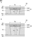
- Fig. 2A is a cross-sectional view showing an example of the circuit board according to the first embodiment of the present invention
- Fig. 2B is a cross-sectional view showing an example of the circuit board at a position different from that shown in Fig. 2A.
- 3A and 3B are schematic views for explaining a method for measuring the height of the first interlayer connection conductor, the height of the first portion, and the height of the second portion.
- 4A to 4D are cross-sectional views that diagrammatically show an example of a process for preparing a first base material filled with a first material and a second material.
- FIG. 5A to 5D are cross-sectional views that diagrammatically show an example of a process for preparing a second base material filled with a first material and a second material.
- FIG. 6 is a cross-sectional view that illustrates an example of a step of laminating base materials.
- FIG. 7 is a cross-sectional view showing an example of a collective pressing process.
- Fig. 8A is a cross-sectional view showing an example of a circuit board according to a second embodiment of the present invention
- Fig. 8B is a cross-sectional view showing an example of the circuit board at a position different from that shown in Fig. 8A.
- FIG. 9 is a cross-sectional view illustrating an example of a circuit board according to a third embodiment of the present invention.
- FIG. 10 is a cross-sectional view illustrating another example of the circuit board according to the fourth embodiment of the present invention.
- FIG. 11 is a cross-sectional view illustrating an example of a circuit board according to a fifth embodiment of the present invention.
- FIG. 12 is a cross-sectional view illustrating another example of the circuit board according to the fifth embodiment of the present invention.
- FIG. 13 is a cross-sectional view illustrating an example of a circuit board according to a sixth embodiment of the present invention.
- Fig. 14A is a cross-sectional view showing an example of a circuit board according to a seventh embodiment of the present invention
- Fig. 14B is a cross-sectional view showing an example of the circuit board at a position different from that shown in Fig. 14A.
- FIG. 15 is a cross-sectional view illustrating an example of a circuit board according to an eighth embodiment of the present invention.
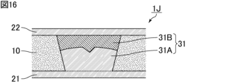
- FIG. 16 is a cross-sectional view illustrating an example of a circuit board according to a ninth embodiment of the present invention.
- FIG. 17 is a cross-sectional view illustrating a schematic diagram of another example of the circuit board according to the ninth embodiment of the present invention.
- 18A, 18B, and 18C are cross-sectional views that typically show examples of a circuit board according to a tenth embodiment of the present invention.
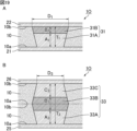
- Fig. 19A is a cross-sectional view showing an example of a circuit board according to an eleventh embodiment of the present invention, and Fig.
- FIG. 19B is a cross-sectional view showing an example of the circuit board at a position different from that shown in Fig. 19A.
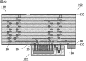
- FIG. 20 is a cross-sectional view that illustrates an example of a circuit module including a circuit board according to the present invention.
- the circuit board of the present invention will now be described.
- the present invention is not limited to the following configurations, and can be appropriately modified and applied within the scope of the present invention.
- the present invention also includes a combination of two or more of the individual preferred configurations of the present invention described below.
- terms indicating the relationship between elements are not expressions that only express a strict meaning, but are expressions that mean that they are substantially equivalent, for example, including differences of about a few percent.
- “equivalent” is an expression that does not only mean that they are completely equivalent, but is an expression that means that they are substantially equivalent, for example, including differences of about a few percent.
- FIG. 1 is a cross-sectional view showing a schematic example of a circuit board according to the present invention.
- the circuit board 1 shown in FIG. 1 includes an insulating layer 10, a conductor layer 20, and an interlayer connection conductor 30.
- the circuit board 1 is a multilayer circuit board having multiple insulating layers 10.
- the circuit board 1 may be a rigid board or a flexible board.
- the circuit board 1 may have a bent portion.
- the conductor layer 20 includes a first conductor layer, a second conductor layer, a third conductor layer, and a fourth conductor layer, which will be described in each embodiment below.
- the conductor layer 20 may include a fifth conductor layer and a sixth conductor layer.
- the conductor layer 20 may include a fifth conductor layer and a sixth conductor layer instead of the third conductor layer and the fourth conductor layer.
- the circuit board 1 may include a conductor layer 20 other than the first conductor layer, the second conductor layer, the third conductor layer, the fourth conductor layer, the fifth conductor layer, and the sixth conductor layer.
- the interlayer connection conductor 30 includes a first interlayer connection conductor and a second interlayer connection conductor, which will be described in each embodiment below. Specifically, it is sufficient that the circuit board 1 includes at least one first interlayer connection conductor and at least one second interlayer connection conductor.
- the interlayer connection conductor 30 may include a third interlayer connection conductor in addition to the first interlayer connection conductor and the second interlayer connection conductor. Specifically, at least one first interlayer connection conductor, at least one second interlayer connection conductor, and at least one third interlayer connection conductor may be included in the circuit board 1.
- the interlayer connection conductor 30 may include a third interlayer connection conductor instead of the second interlayer connection conductor.
- at least one first interlayer connection conductor and at least one third interlayer connection conductor may be included in the circuit board 1.
- the circuit board 1 may include interlayer connection conductors 30 other than the first interlayer connection conductor, the second interlayer connection conductor, and the third interlayer connection conductor.
- FIG. 2A is a cross-sectional view showing an example of a circuit board according to a first embodiment of the present invention.
- FIG. 2B is a cross-sectional view showing an example of a circuit board in a position different from that shown in FIG. 2A.
- the circuit board 1A includes an insulating layer 10, a first conductor layer 21, a second conductor layer 22, a third conductor layer 23, a fourth conductor layer 24, a first interlayer connection conductor 31, and a second interlayer connection conductor 32.
- the insulating layer 10 has a first main surface 10a and a second main surface 10b that face each other in the thickness direction (the up-down direction in Figures 2A and 2B).
- the insulating layer 10 is, for example, a resin insulating layer whose main component is resin.
- the loss during signal transmission can be reduced by forming the insulating layer 10 from a resin having a low dielectric constant.
- the insulating layer 10 may be a ceramic insulating layer whose main component is ceramic.
- the insulating layer 10 is made of a ceramic having a high dielectric constant, making it possible to radiate or receive in a wide band.
- the resin that constitutes the resin insulation layer may be a thermosetting resin or a thermoplastic resin, but is preferably a thermoplastic resin.
- the resin insulation layer is made of a thermoplastic resin, multiple resin sheets on which conductor layers are formed can be stacked and collectively compressed (collectively pressed) by heat treatment.
- Thermosetting resins include epoxy resins, phenolic resins, polyimide resins or modified resins thereof, and acrylic resins.
- thermoplastic resins include liquid crystal polymers (LCPs), fluororesins, thermoplastic polyimide resins, polyether ether ketone resins (PEEK), polyphenylene sulfide resins (PPS), etc.
- LCPs liquid crystal polymers
- PEEK polyether ether ketone resins
- PPS polyphenylene sulfide resins
- the resin insulation layer is preferably made of liquid crystal polymer (LCP).
- LCP liquid crystal polymer
- Liquid crystal polymer has a lower water absorption rate than other thermoplastic resins. Therefore, when the resin insulation layer is made of liquid crystal polymer, the amount of moisture remaining in the resin insulation layer can be reduced.
- the resin insulation layer may contain inorganic materials such as ceramic fillers.
- Ceramic fillers include, for example, boron nitride, talc, and fused silica.
- Examples of the ceramic that constitutes the ceramic insulating layer include low-temperature co-fired ceramic (LTCC) and high-temperature co-fired ceramic (HTCC).
- LTCC low-temperature co-fired ceramic
- HTCC high-temperature co-fired ceramic
- each insulating layer 10 is preferably 10 ⁇ m or more and 100 ⁇ m or less.
- the first conductor layer 21 is provided on the first main surface 10a of the insulating layer 10 and is connected to the first interlayer connection conductor 31.
- the second conductor layer 22 is provided on the second main surface 10b of the insulating layer 10 and is connected to the first interlayer connection conductor 31.
- the first conductor layer 21 and the second conductor layer 22 may each have a pattern shape patterned into wiring or the like, or may have a surface shape that spreads over one surface.
- the shapes of the first conductor layer 21 and the second conductor layer 22 may be the same as each other or may be different.
- the first conductor layer 21 and the second conductor layer 22 are each a metal layer containing at least one of the following metals, for example: copper, silver, aluminum, stainless steel, nickel, and gold.
- the materials of the first conductor layer 21 and the second conductor layer 22 may be the same as or different from each other.
- Both the first conductor layer 21 and the second conductor layer 22 are preferably made of a metal foil, and more preferably made of copper (Cu) foil.
- the first conductor layer 21 and the second conductor layer 22 may each have a matte surface on one main surface and a shiny surface on the other main surface.
- the thickness (length in the stacking direction) of the first conductor layer 21 and the second conductor layer 22 is preferably 1 ⁇ m or more and 35 ⁇ m or less, and more preferably 6 ⁇ m or more and 18 ⁇ m or less.
- the thicknesses of the first conductor layer 21 and the second conductor layer 22 may be the same as or different from each other.
- the first conductor layer 21 and the second conductor layer 22 may or may not be parallel to each other.
- One insulating layer 10 may be provided between the first conductor layer 21 and the second conductor layer 22, or two or more insulating layers 10 may be provided.
- the configurations of the insulating layers 10 may be the same as each other or different.
- the thicknesses of the insulating layers 10 may be the same as each other or different.
- the third conductor layer 23 is provided on the first main surface 10a of the insulating layer 10 and is connected to the second interlayer connection conductor 32.
- the fourth conductor layer 24 is provided on the second main surface 10b of the insulating layer 10 and is connected to the second interlayer connection conductor 32.
- the third conductor layer 23 and the fourth conductor layer 24 may each have a pattern shape patterned into wiring or the like, or may have a surface shape that spreads over one surface.
- the shapes of the third conductor layer 23 and the fourth conductor layer 24 may be the same as each other or may be different.
- the third conductor layer 23 and the fourth conductor layer 24 are each a metal layer containing at least one of the following metals, for example: copper, silver, aluminum, stainless steel, nickel, and gold.
- the materials of the third conductor layer 23 and the fourth conductor layer 24 may be the same as or different from each other.
- Both the third conductor layer 23 and the fourth conductor layer 24 are preferably made of metal foil, and more preferably made of copper (Cu) foil.
- the third conductor layer 23 and the fourth conductor layer 24 may each have a matte surface on one main surface and a shiny surface on the other main surface.
- the thickness (length in the stacking direction) of the third conductor layer 23 and the fourth conductor layer 24 is preferably 1 ⁇ m or more and 35 ⁇ m or less, and more preferably 6 ⁇ m or more and 18 ⁇ m or less.
- the thicknesses of the third conductor layer 23 and the fourth conductor layer 24 may be the same as or different from each other.
- the third conductor layer 23 and the fourth conductor layer 24 may or may not be parallel to each other.
- One insulating layer 10 may be provided between the third conductor layer 23 and the fourth conductor layer 24, or two or more insulating layers 10 may be provided.
- the configurations of the insulating layers 10 may be the same as each other or different.
- the thicknesses of the insulating layers 10 may be the same as each other or different.
- the first interlayer connection conductor 31 and the second interlayer connection conductor 32 are provided penetrating the insulating layer 10 in the thickness direction.
- the first interlayer connection conductor 31 is provided so as to penetrate the insulating layer 10 in the thickness direction but not through the first conductor layer 21 and the second conductor layer 22, and to be connected to the first conductor layer 21 and the second conductor layer 22. Therefore, the first interlayer connection conductor 31 penetrates the insulating layer 10 in the thickness direction by the number of layers provided between the first conductor layer 21 and the second conductor layer 22. For example, the first interlayer connection conductor 31 is provided so as to penetrate one insulating layer 10 in the thickness direction.
- the second interlayer connection conductor 32 is provided so as to penetrate the insulating layer 10 in the thickness direction but not through the third conductor layer 23 and the fourth conductor layer 24, and to be connected to the third conductor layer 23 and the fourth conductor layer 24. Therefore, the second interlayer connection conductor 32 penetrates the insulating layer 10 in the thickness direction by the number of layers provided between the third conductor layer 23 and the fourth conductor layer 24. For example, the second interlayer connection conductor 32 is provided so as to penetrate one insulating layer 10 in the thickness direction.
- the insulating layer 10 on which the first interlayer connection conductor 31 is provided may be the same layer as the insulating layer 10 on which the second interlayer connection conductor 32 is provided, or may be a different layer, but it is preferable that they are different layers. In that case, it is preferable that the thickness of the insulating layer 10 on which the first interlayer connection conductor 31 is provided is smaller than the thickness of the insulating layer 10 on which the second interlayer connection conductor 32 is provided.
- the insulating layer 10 on which the first interlayer connection conductor 31 is provided is a layer different in the thickness direction from the insulating layer 10 on which the second interlayer connection conductor 32 is provided.
- the insulating layer 10 on which the first interlayer connection conductor 31 is provided and the insulating layer 10 on which the second interlayer connection conductor 32 is provided may be adjacent in the thickness direction, and at least one insulating layer 10 may be disposed between the insulating layer 10 on which the first interlayer connection conductor 31 is provided and the insulating layer 10 on which the second interlayer connection conductor 32 is provided.
- the shape of the first interlayer connection conductor 31 and the second interlayer connection conductor 32 is preferably circular. In this case, not only a perfect circle but also an ellipse, an oval, etc. are included in the circle.
- the cross-sectional shapes of the first interlayer connection conductor 31 and the second interlayer connection conductor 32 may be the same as each other or may be different.
- the first interlayer connection conductor 31 includes a first portion 31A and a second portion 31B in the thickness direction.
- the first portion 31A is, for example, a plated via.
- a plated via means a film grown by a liquid phase method or a vapor phase method.
- the metal contained in the first portion 31A is preferably the same as the metal constituting the first conductor layer 21, e.g., Cu.
- the second portion 31B has a lower conductivity than the first portion 31A.
- the second portion 31B is, for example, a paste via.
- a paste via means a solidified paste.
- the second portion 31B functions as a bonding material, thereby electrically connecting the first portion 31A and the second conductor layer 22.
- examples of the metal contained in the second portion 31B include Cu, Sn, Ag, Ni, Cr, Pt, Mo, Ga, Ge, Sb, In, Pb, and alloys containing at least one of these metals.
- the metal contained in the second portion 31B may be the same as or different from the metal contained in the first portion 31A.
- the metal contained in the second portion 31B is, for example, an alloy containing Cu and Sn.
- the second portion 31B may be a plated via.
- the metal contained in the second portion 31B may be, for example, Sn.
- Sn which has a low melting point, the second portion 31B can easily function as a bonding material.
- One end of the first portion 31A is joined to the first conductor layer 21, and the other end of the first portion 31A is joined to one end of the second portion 31B.
- the first portion 31A and the first conductor layer 21 are directly bonded, without any dissimilar materials in between. Therefore, at the interface between the first portion 31A and the first conductor layer 21, there is a portion where no dissimilar materials are present, i.e., a portion where the first portion 31A and the first conductor layer 21 are in direct contact.
- the other end of the second portion 31B is joined to the second conductor layer 22.
- the second interlayer connection conductor 32 includes a third portion 32A and a fourth portion 32B in the thickness direction.
- the third portion 32A is, for example, a plated via.
- the metal contained in the third portion 32A is preferably the same as the metal constituting the third conductor layer 23, e.g., Cu.
- the metal contained in the third portion 32A is preferably the same as the metal contained in the first portion 31A.
- the fourth portion 32B has a lower conductivity than the third portion 32A.
- the fourth portion 32B is, for example, a paste via.
- the fourth portion 32B functions as a bonding material, thereby electrically connecting the third portion 32A and the fourth conductor layer 24.
- examples of the metal contained in the fourth portion 32B include Cu, Sn, Ag, Ni, Cr, Pt, Mo, Ga, Ge, Sb, In, Pb, and alloys containing at least one of these metals.
- the metal contained in the fourth portion 32B may be the same as or different from the metal contained in the third portion 32A.
- the metal contained in the fourth portion 32B is, for example, an alloy containing Cu and Sn. It is preferable that the metal contained in the fourth portion 32B is the same as the metal contained in the second portion 31B.
- the fourth portion 32B may be a plated via.
- the metal contained in the fourth portion 32B may be, for example, Sn.
- Sn which has a low melting point
- the fourth portion 32B can easily function as a bonding material. It is preferable that the metal contained in the fourth portion 32B is the same as the metal contained in the second portion 31B.
- One end of the third portion 32A is joined to the third conductor layer 23, and the other end of the third portion 32A is joined to one end of the fourth portion 32B.
- the third portion 32A and the third conductor layer 23 are directly bonded to each other without using a different material. Therefore, at the interface between the third portion 32A and the third conductor layer 23, there is a portion where no different material exists, i.e., a portion where the third portion 32A and the third conductor layer 23 are in direct contact.
- the other end of the fourth portion 32B is joined to the fourth conductor layer 24.
- the second interlayer connection conductor 32 which has a greater height, has a smaller proportion of low conductivity portions than the first interlayer connection conductor 31, which has a smaller height. This makes it possible to suppress an increase in the resistance value of the entire interlayer connection conductor, even when interlayer connection conductors of different heights are included.
- the first interlayer connection conductor 31 and the second interlayer connection conductor 32 have a smaller proportion of the portion with high conductivity compared to the second interlayer connection conductor 32, which has a larger height.
- the first portion 31A is a plated via and the second portion 31B is a paste via, an increase in manufacturing costs can be suppressed by not forming the first portion 31A more than necessary.
- the height B1 of the second portion 31B is equal to the height B2 of the fourth portion 32B. Note that, as long as the relationships T1 ⁇ T2 and B1 / A1 > B2 / A2 are satisfied, the height B1 of the second portion 31B may be greater than the height B2 of the fourth portion 32B or may be smaller than the height B2 of the fourth portion 32B.
- the diameter of the first interlayer connection conductor 31 is preferably smaller than the diameter of the second interlayer connection conductor 32. Note that, as long as the relationships T1 ⁇ T2 and B1 / A1 > B2 / A2 are satisfied, the diameter of the first interlayer connection conductor 31 may be equal to or larger than the diameter of the second interlayer connection conductor 32.
- first interlayer connection conductors 31 There may be two or more types of first interlayer connection conductors 31 having different diameters and a height T1 . In this case, it is preferable that the height A1 of the first portion 31A of the first interlayer connection conductor 31 having a larger diameter is smaller than the height A1 of the first portion 31A of the first interlayer connection conductor 31 having a smaller diameter.
- the height A2 of the third portion 32A of the second interlayer connection conductor 32 having a larger diameter is smaller than the height A2 of the third portion 32A of the second interlayer connection conductor 32 having a smaller diameter.
- the height A1 of the first portion 31A may be equal to the height B1 of the second portion 31B or may be lower than the height B1 of the second portion 31B ( A1 ⁇ B1 ), but is preferably higher than the height B1 of the second portion 31B ( A1 > B1 ).
- the first interlayer connection conductor 31 has a tapered shape, making the height A1 of the first portion 31A higher than the height B1 of the second portion 31B increases the connection area between the first portion 31A and the second portion 31B, thereby improving the connection reliability of the first interlayer connection conductor 31.
- the height A2 of the third portion 32A may be equal to the height B2 of the fourth portion 32B or may be lower than the height B2 of the fourth portion 32B ( A2 ⁇ B2 ), but is preferably higher than the height B2 of the fourth portion 32B ( A2 > B2 ).
- the second interlayer connection conductor 32 has a tapered shape, making the height A2 of the third portion 32A higher than the height B2 of the fourth portion 32B increases the connection area between the third portion 32A and the fourth portion 32B, thereby improving the connection reliability of the second interlayer connection conductor 32.
- the shape of the first interlayer connection conductor 31 is not limited to that shown in FIG. 2A.
- the second portion 31B may have a tapered shape in which the area of the end face on the first conductor layer 21 side is smaller than the area of the end face on the second conductor layer 22 side.
- the inclination angle of the tapered shape may vary in stages. In this case, the connection strength between the second portion 31B and the second conductor layer 22 can be further increased.
- the inclination angle of the tapered shape may change in two stages, three stages, or four or more stages.
- the first portion 31A may have a tapered shape in which the area of the end face on the first conductor layer 21 side is smaller than the area of the end face on the second conductor layer 22 side.
- the inclination angle of the tapered shape may vary in stages. In that case, the inclination angle of the tapered shape may change in two stages, three stages, or four or more stages.
- the first interlayer connection conductor 31 may have a tapered shape in which the area of the end face on the first conductor layer 21 side is smaller than the area of the end face on the second conductor layer 22 side, as shown in FIG. 2A.
- the first interlayer connection conductor 31 may have a shape in which the area of the end face on the first conductor layer 21 side is equal to the area of the end face on the second conductor layer 22 side. In other words, the first interlayer connection conductor 31 does not have to have a tapered shape.
- the first portion 31A may have a shape in which the area of the end face on the first conductor layer 21 side is equal to the area of the end face on the second conductor layer 22 side
- the second portion 31B may have a shape in which the area of the end face on the first conductor layer 21 side is equal to the area of the end face on the second conductor layer 22 side.
- first interlayer connection conductor 31 has a tapered shape as shown in FIG. 2A, strain stress tends to concentrate at the necking points of the first interlayer connection conductor 31 (particularly, at the necking points between the first interlayer connection conductor 31 and the first conductor layer 21). In contrast, if the first interlayer connection conductor 31 does not have a tapered shape, the concentration of strain stress at the necking points of the first interlayer connection conductor 31 is eliminated. Therefore, the stress acting on the first interlayer connection conductor 31 is distributed, improving connection reliability.
- the end face of the first portion 31A on the second conductor layer 22 side is flat, but as described below, it may protrude toward the second conductor layer 22 or may be recessed toward the first conductor layer 21.
- the shape of the second interlayer connection conductor 32 is not limited to that shown in FIG. 2B.
- the fourth portion 32B may have a tapered shape in which the area of the end face on the third conductor layer 23 side is smaller than the area of the end face on the fourth conductor layer 24 side.
- the inclination angle of the tapered shape may vary in stages. In this case, the connection strength between the fourth portion 32B and the fourth conductor layer 24 can be further increased.
- the inclination angle of the tapered shape may change in two stages, three stages, or four or more stages.
- the third portion 32A may have a tapered shape in which the area of the end face on the third conductor layer 23 side is smaller than the area of the end face on the fourth conductor layer 24 side.
- the inclination angle of the tapered shape may vary in stages. In that case, the inclination angle of the tapered shape may change in two stages, three stages, or four or more stages.
- the second interlayer connection conductor 32 may have a tapered shape in which the area of the end face on the third conductor layer 23 side is smaller than the area of the end face on the fourth conductor layer 24 side, as shown in FIG. 2B.
- the second interlayer connection conductor 32 may have a shape in which the area of the end face on the third conductor layer 23 side is equal to the area of the end face on the fourth conductor layer 24 side. In other words, the second interlayer connection conductor 32 does not have to have a tapered shape.
- the third portion 32A may have a shape in which the area of the end face on the third conductor layer 23 side is equal to the area of the end face on the fourth conductor layer 24 side
- the fourth portion 32B may have a shape in which the area of the end face on the third conductor layer 23 side is equal to the area of the end face on the fourth conductor layer 24 side.
- the end face of the third portion 32A on the side of the fourth conductor layer 24 is flat, but like the first interlayer connection conductor 31, it may protrude toward the fourth conductor layer 24 or may be recessed toward the third conductor layer 23.
- FIGS. 3A and 3B are schematic diagrams for explaining a method for measuring the height of the first interlayer connection conductor, the height of the first portion, and the height of the second portion.
- the cross section is polished in slices at intervals of 5 ⁇ m from the front of the first interlayer connection conductor 31 to be measured (the position indicated by L1 in Fig. 3A).
- the cross section is polished in slices at regular intervals in the depth direction while being scraped with coarse abrasive paper.
- finish polishing is performed using fine abrasive paper.
- the height T 2 of the second interlayer connection conductor 32, the height A 2 of the third portion 32A, and the height B 2 of the fourth portion 32B can also be measured by obtaining their cross sections in a similar manner.
- the circuit board 1A is manufactured, for example, by the following method. Note that the circuit board 1A may be manufactured in one-chip (individual piece) state, or may be manufactured by producing an aggregate board and then separating it into individual pieces.
- the aggregate board here refers to a board that includes multiple circuit boards 1A.
- FIGS. 4A to 4D are cross-sectional views that show a schematic example of a process for preparing a first substrate filled with a first material and a second material.
- a first substrate 61 is prepared, in which a conductor layer 20 is formed on one main surface of an insulating layer 10.
- a metal foil such as Cu foil is laminated onto one main surface of the insulating layer 10, and the metal foil is patterned by photolithography to form the conductor layer 20.
- the insulating layer 10 is, for example, a resin sheet whose main component is a thermoplastic resin such as a liquid crystal polymer.
- a via hole 70 is formed in the first substrate 61, which penetrates the insulating layer 10 and exposes a portion of the upper surface of the conductor layer 20. It is preferable that the via hole 70 has a tapered shape in which the hole diameter becomes smaller toward the conductor layer 20.
- a via hole 70 is formed in the insulating layer 10 using a laser or the like so that the top surface of the conductor layer 20 is exposed.
- the via hole 70 is filled with a first material 71.
- the first material 71 is filled partway into the via hole 70. There are no particular limitations on the height of the first material 71, so long as it does not exceed the thickness of the insulating layer 10.
- a plating process such as electrolytic plating is used to fill the via hole 70 with a plating metal such as Cu as a first material 71.
- the first material 71 forms the first portion 31A (see FIG. 7).
- the second material 72 is filled into the via hole 70 after it has been filled with the first material 71.
- the space in the via hole 70 is filled with the first material 71 and the second material 72.
- a conductive paste containing a metal material such as Cu or Sn and a resin material is filled as the second material 72.
- the second material 72 is solidified by a heating press described later, thereby forming the second portion 31B (see FIG. 7).
- the via hole 70 It is also possible to fill the via hole 70 with a plating metal such as Sn as the second material 72, but depending on the metal selected as the second material 72, there is a risk that the metal of the underlying first material 71 will remelt. Therefore, from the viewpoint of increasing the degree of freedom in selecting the first material 71 and the second material 72, it is preferable to fill the via hole 70 with a plating metal as the first material 71 and then fill it with a conductive paste as the second material 72.
- a plating metal such as Sn
- FIGS. 5A to 5D are cross-sectional views that show a schematic example of a process for preparing a second substrate filled with a first material and a second material.
- the method shown in FIG. 5A to FIG. 5D is similar to the method shown in FIG. 4A to FIG. 4D.
- a second substrate 62 is prepared, in which a conductor layer 20 is formed on one main surface of an insulating layer 10.
- a metal foil such as Cu foil is laminated onto one main surface of the insulating layer 10, and the metal foil is patterned by photolithography to form the conductor layer 20.
- the insulating layer 10 is, for example, a resin sheet whose main component is a thermoplastic resin such as a liquid crystal polymer.
- a via hole 70 is formed in the second substrate 62, penetrating the insulating layer 10 and exposing a portion of the upper surface of the conductor layer 20. It is preferable that the via hole 70 has a tapered shape in which the hole diameter becomes smaller toward the conductor layer 20.
- a via hole 70 is formed in the insulating layer 10 using a laser or the like so that the top surface of the conductor layer 20 is exposed.
- the via hole 70 is filled with a first material 71.
- the first material 71 is filled partway into the via hole 70. There are no particular limitations on the height of the first material 71, so long as it does not exceed the thickness of the insulating layer 10.
- a plating process such as electrolytic plating is used to fill the via hole 70 with a plating metal such as Cu as a first material 71.
- the first material 71 forms the third portion 32A (see FIG. 7).
- the second material 72 is filled into the via hole 70 after it has been filled with the first material 71.
- the space in the via hole 70 is filled with the first material 71 and the second material 72.
- a conductive paste containing a metal material such as Cu or Sn and a resin material is filled as the second material 72.
- the second material 72 is solidified by a heating press described later, thereby forming the fourth portion 32B (see FIG. 7).
- the via hole 70 It is also possible to fill the via hole 70 with a plating metal such as Sn as the second material 72, but depending on the metal selected as the second material 72, there is a risk that the metal of the underlying first material 71 will remelt. Therefore, from the viewpoint of increasing the degree of freedom in selecting the first material 71 and the second material 72, it is preferable to fill the via hole 70 with a plating metal as the first material 71 and then fill it with a conductive paste as the second material 72.
- a plating metal such as Sn
- Figure 6 is a cross-sectional view that shows a schematic example of a process for laminating substrates.
- FIG. 6 shows an example in which a substrate 60 not filled with a first material 71 and a second material 72, a first substrate 61 filled with a first material 71 and a second material 72, and a second substrate 62 filled with a first material 71 and a second material 72 are laminated, but there is no particular limitation as long as a first interlayer connection conductor 31 and a second interlayer connection conductor 32 as shown in FIG. 7 are formed.
- Figure 7 is a cross-sectional view that shows a schematic example of a batch pressing process.
- the circuit board 1A can be easily manufactured by pressing the insulating layer 10 all at once. This reduces the number of manufacturing steps for the circuit board 1A, and keeps manufacturing costs low.
- an anti-rust layer 40 (see FIG. 8A) described later may be provided at least at the interface between the first conductor layer 21 and the insulating layer 10.
- an anti-rust layer 40 (see FIG. 8B) described later may be provided at least at the interface between the third conductor layer 23 and the insulating layer 10. The same applies to the following embodiments.
- the anti-rust layer 40 is formed by applying an anti-rust treatment to the surface of the metal foil using a metal such as Zn, Ni, Cr, Mo, or Pt.
- the circuit board 1A is produced by the above-mentioned batch pressing, by disposing the rust-proof layer 40 at the interface between the first conductor layer 21 or the third conductor layer 23 and the insulating layer 10, oxidation of the metal foil such as Cu foil constituting the first conductor layer 21 or the third conductor layer 23 is prevented, and therefore a decrease in adhesion between the first conductor layer 21 or the third conductor layer 23 and the insulating layer 10 can be suppressed.
- the thermal load on the interface between the first conductor layer 21 or the third conductor layer 23 and the insulating layer 10 is greater than the thermal load on the interface between the second conductor layer 22 or the fourth conductor layer 24 and the insulating layer 10. Therefore, it is preferable that the anti-corrosion layer 40 is disposed at least at the interface between the first conductor layer 21 or the third conductor layer 23 and the insulating layer 10.
- the anti-rust layer 40 When the anti-rust layer 40 is disposed at the interface between the first conductor layer 21 and the insulating layer 10, the anti-rust layer 40 may or may not be in contact with the first portion 31A. Similarly, when the anti-rust layer 40 is disposed at the interface between the third conductor layer 23 and the insulating layer 10, the anti-rust layer 40 may or may not be in contact with the third portion 32A.
- the anti-rust layer 40 is not disposed between the first portion 31A and the first conductor layer 21. Similarly, it is preferable that the anti-rust layer 40 is not disposed between the third portion 32A and the third conductor layer 23.
- the anti-rust layer 40 is not disposed at the interface between the second conductor layer 22 and the insulating layer 10. Similarly, it is preferable that the anti-rust layer 40 is not disposed at the interface between the fourth conductor layer 24 and the insulating layer 10.
- the anti-rust layer 40 is not disposed between the second portion 31B and the second conductor layer 22. Similarly, it is preferable that the anti-rust layer 40 is not disposed between the fourth portion 32B and the fourth conductor layer 24.
- FIG. 8A is a cross-sectional view showing an example of a circuit board according to a second embodiment of the present invention.
- FIG. 8B is a cross-sectional view showing an example of a circuit board in a position different from that shown in FIG. 8A.
- the surface roughness of the first conductor layer 21 in contact with the insulating layer 10 is greater than the surface roughness of the second conductor layer 22 in contact with the insulating layer 10. Furthermore, as shown in FIG. 8B, the surface roughness of the third conductor layer 23 in contact with the insulating layer 10 is greater than the surface roughness of the fourth conductor layer 24 in contact with the insulating layer 10.
- the surface roughness of the first conductor layer 21 in contact with the insulating layer 10 is greater than the surface roughness of the second conductor layer 22 in contact with the insulating layer 10
- the surface roughness of the third conductor layer 23 in contact with the insulating layer 10 may be less than the surface roughness of the fourth conductor layer 24 in contact with the insulating layer 10, or may be equal to the surface roughness of the fourth conductor layer 24 in contact with the insulating layer 10.
- the surface roughness of the third conductor layer 23 in contact with the insulating layer 10 is greater than the surface roughness of the fourth conductor layer 24 in contact with the insulating layer 10
- the surface roughness of the first conductor layer 21 in contact with the insulating layer 10 may be less than the surface roughness of the second conductor layer 22 in contact with the insulating layer 10, or may be equal to the surface roughness of the second conductor layer 22 in contact with the insulating layer 10.
- an anti-rust layer 40 is provided at the interface between the first conductor layer 21 and the insulating layer 10, but the anti-rust layer 40 does not have to be provided at the interface between the first conductor layer 21 and the insulating layer 10.
- an anti-rust layer 40 is provided at the interface between the third conductor layer 23 and the insulating layer 10, but the anti-rust layer 40 does not have to be provided at the interface between the third conductor layer 23 and the insulating layer 10.
- FIG. 9 is a cross-sectional view showing a schematic example of a circuit board according to a third embodiment of the present invention.
- the end face of the first portion 31A on the second conductor layer 22 side protrudes toward the second conductor layer 22.
- the end faces of the first portion 31A on the second conductor layer 22 side protrude symmetrically.
- FIG. 10 is a cross-sectional view showing a schematic diagram of another example of a circuit board according to the fourth embodiment of the present invention.
- the end face of the first portion 31A on the second conductor layer 22 side protrudes toward the second conductor layer 22, as in FIG. 9.
- the end face of the first portion 31A on the second conductor layer 22 side protrudes asymmetrically.
- connection area between the first portion 31A and the second portion 31B becomes large, and the connection strength between the first portion 31A and the second portion 31B can be increased.
- the height A1 of the first portion 31A may be equal to or lower than the height B1 of the second portion 31B ( A1 ⁇ B1 ), but is preferably higher than the height B1 of the second portion 31B ( A1 > B1 ). Note that the height A1 of the first portion 31A is defined as the height of the highest portion, and the height B1 of the second portion 31B is defined as the height of the lowest portion.
- the end face of the third portion 32A of the second interlayer connection conductor 32 on the fourth conductor layer 24 side may also protrude toward the fourth conductor layer 24.
- the end face of the third portion 32A on the fourth conductor layer 24 side may protrude symmetrically or asymmetrically.
- the height A2 of the third portion 32A may be equal to the height B2 of the fourth portion 32B or may be lower than the height B2 of the fourth portion 32B ( A2 ⁇ B2 ), but is preferably higher than the height B2 of the fourth portion 32B ( A2 > B2 ).
- the height A2 of the third portion 32A is defined as the height of the highest portion
- the height B2 of the fourth portion 32B is defined as the height of the lowest portion.
- FIG. 11 is a cross-sectional view showing a schematic example of a circuit board according to a fifth embodiment of the present invention.
- the end face of the first portion 31A facing the second conductor layer 22 is recessed toward the first conductor layer 21.
- the end face of the first portion 31A facing the second conductor layer 22 is recessed symmetrically.
- FIG. 12 is a cross-sectional view showing a schematic diagram of another example of a circuit board according to the fifth embodiment of the present invention.
- the end face of the first portion 31A facing the second conductor layer 22 is recessed toward the first conductor layer 21, as in FIG. 11.
- the end face of the first portion 31A facing the second conductor layer 22 is recessed asymmetrically.
- connection area between the first portion 31A and the second portion 31B becomes large, and the connection strength between the first portion 31A and the second portion 31B can be increased.
- the height A1 of the first portion 31A may be equal to the height B1 of the second portion 31B or may be lower than the height B1 of the second portion 31B ( A1 ⁇ B1 ), but is preferably higher than the height B1 of the second portion 31B ( A1 > B1 ). Note that the height A1 of the first portion 31A is defined as the height of the lowest portion, and the height B1 of the second portion 31B is defined as the height of the highest portion.
- the valley has one apex, but there may be two or more.
- the size, depth, shape, etc. of the valley may be the same or different.
- the end face of the first portion 31A on the second conductor layer 22 side may include a mixture of a portion that protrudes toward the second conductor layer 22 and a portion that is recessed toward the first conductor layer 21.
- the end face of the third portion 32A of the second interlayer connection conductor 32 on the fourth conductor layer 24 side may also be recessed toward the third conductor layer 23. In that case, the end face of the third portion 32A on the fourth conductor layer 24 side may be recessed symmetrically or asymmetrically.
- the height A2 of the third portion 32A may be equal to the height B2 of the fourth portion 32B or may be lower than the height B2 of the fourth portion 32B ( A2 ⁇ B2 ), but is preferably higher than the height B2 of the fourth portion 32B ( A2 > B2 ).
- the height A2 of the third portion 32A is defined as the height of the lowest portion
- the height B2 of the fourth portion 32B is defined as the height of the highest portion.
- the end face of the third portion 32A on the fourth conductor layer 24 side may include a mixture of a portion that protrudes toward the fourth conductor layer 24 and a portion that is recessed toward the third conductor layer 23.
- FIG. 13 is a cross-sectional view showing a schematic example of a circuit board according to a sixth embodiment of the present invention.
- the end face of the first portion 31A on the first conductor layer 21 side protrudes toward the first conductor layer 21 side beyond the interface between the first conductor layer 21 and the insulating layer 10.
- connection area between the first portion 31A and the first conductor layer 21 becomes larger, and the connection strength between the first portion 31A and the first conductor layer 21 can be increased.
- the end face of the first portion 31A on the first conductor layer 21 side protrudes symmetrically, but it may also protrude asymmetrically.
- the mountain has one vertex, but it may have two or more vertices.
- the size, height, shape, etc. of the mountain may be the same or different.
- the end face of the third portion 32A of the second interlayer connection conductor 32 on the third conductor layer 23 side may also protrude toward the third conductor layer 23 side beyond the interface between the third conductor layer 23 and the insulating layer 10.
- the end face of the third portion 32A on the third conductor layer 23 side may protrude symmetrically or asymmetrically.
- FIG. 14A is a cross-sectional view showing an example of a circuit board according to a seventh embodiment of the present invention.
- FIG. 14B is a cross-sectional view showing an example of a circuit board in a position different from that shown in FIG. 14A.
- the first portion 31A is bonded to the second portion 31B via a first intermediate layer 51 that includes the metal contained in the first portion 31A and the metal contained in the second portion 31B, and is also bonded to the first conductor layer 21 without the first intermediate layer 51.
- a first intermediate layer 51 containing Cu and Sn is formed on the end of the second portion 31B on the first portion 31A side.
- the first intermediate layer 51 is made of a Cu-Sn alloy such as Cu 3 Sn or Cu 5 Sn.
- the composition of the first intermediate layer 51 is different from the composition of the second portion 31B.
- the second portion 31B is joined to the second conductor layer 22 via a second intermediate layer 52 that contains the metal contained in the second portion 31B and the metal contained in the second conductor layer 22.
- a second intermediate layer 52 containing Cu and Sn is formed in the second portion 31B at the end on the second conductor layer 22 side.
- the second intermediate layer 52 is made of a Cu-Sn alloy such as Cu 3 Sn or Cu 5 Sn, for example.
- the composition of the second intermediate layer 52 is different from the composition of the second portion 31B.
- the first intermediate layer 51 does not have to extend to the interface between the first portion 31A and the insulating layer 10, but may extend to it. If the first intermediate layer 51 extends to the interface between the first portion 31A and the insulating layer 10, the first intermediate layer 51 may reach the interface between the first conductor layer 21 and the insulating layer 10. This can further increase the connection strength between the first portion 31A and the first conductor layer 21.
- the second intermediate layer 52 does not have to extend to the interface between the second conductor layer 22 and the insulating layer 10, but it may.
- the first intermediate layer 51 may be one layer or two or more layers.
- the second intermediate layer 52 may be one layer or two or more layers.
- the first intermediate layer 51 and the second intermediate layer 52 can be confirmed, for example, by observing a cross section of the insulating layer 10 cut in a direction parallel to the thickness direction using a scanning electron microscope (SEM).
- SEM scanning electron microscope
- the first intermediate layer 51 and the second intermediate layer 52 have a different composition from both the first portion 31A and the second portion 31B, and therefore appear in a different color tone from the first portion 31A and the second portion 31B in the SEM photograph.
- compositions such as Cu5Sn , Cu3Sn , and Cu6Sn5 all contain Cu and Sn as metal species, but the content ratio of the metal species is different, so it can be said that they have different compositions.
- the third portion 32A is bonded to the fourth portion 32B via a third intermediate layer 53 that includes the metal contained in the third portion 32A and the metal contained in the fourth portion 32B, and is also bonded to the third conductor layer 23 without the third intermediate layer 53.
- a third intermediate layer 53 containing Cu and Sn is formed on the end of the fourth portion 32B on the third portion 32A side.
- the third intermediate layer 53 is made of a Cu-Sn alloy such as Cu 3 Sn or Cu 5 Sn.
- the composition of the third intermediate layer 53 is different from the composition of the fourth portion 32B.
- the fourth portion 32B is joined to the fourth conductor layer 24 via a fourth intermediate layer 54 that contains the metal contained in the fourth portion 32B and the metal contained in the fourth conductor layer 24.
- a fourth intermediate layer 54 containing Cu and Sn is formed in the fourth portion 32B at the end on the fourth conductor layer 24 side.
- the fourth intermediate layer 54 is made of a Cu-Sn alloy such as Cu 3 Sn or Cu 5 Sn, for example.
- the composition of the fourth intermediate layer 54 is different from the composition of the fourth portion 32B.
- the third intermediate layer 53 does not have to extend to the interface between the third portion 32A and the insulating layer 10, but may extend to it. If the third intermediate layer 53 extends to the interface between the third portion 32A and the insulating layer 10, the third intermediate layer 53 may reach the interface between the third conductor layer 23 and the insulating layer 10. This can further increase the connection strength between the third portion 32A and the third conductor layer 23.
- the fourth intermediate layer 54 does not have to extend to the interface between the fourth conductor layer 24 and the insulating layer 10, but it may.
- the third intermediate layer 53 may be one layer or two or more layers.
- the fourth intermediate layer 54 may be one layer or two or more layers.
- FIG. 15 is a cross-sectional view showing a schematic example of a circuit board according to an eighth embodiment of the present invention.
- part of the end face of the first portion 31A on the second conductor layer 22 side is protruding toward the second conductor layer 22.
- the connection area between the first portion 31A and the second portion 31B becomes large, as in FIG. 9 or FIG. 10, and the connection strength between the first portion 31A and the second portion 31B can be increased.
- a portion of the end face of the first portion 31A on the second conductor layer 22 side may have one protrusion, or two or more protrusions. If two or more protrusions are present, the size, height, shape, etc. of the protrusions may be the same or different.
- the height of the protrusion is, for example, 1 ⁇ m or more and 20 ⁇ m or less. Note that the shape of the protrusion is not limited to the shape shown in FIG. 15.
- the maximum diameter of the protrusion is, for example, 1 ⁇ m or more and 10 ⁇ m or less.
- the maximum diameter of the protrusion refers to the diameter if the cross-sectional shape is circular, and refers to the maximum length passing through the center of the cross-section if the cross-sectional shape is other than circular.
- the second interlayer connection conductor 32 may also have a portion of the end face of the third portion 32A on the fourth conductor layer 24 side that protrudes toward the fourth conductor layer 24.
- FIG. 16 is a cross-sectional view showing a schematic example of a circuit board according to a ninth embodiment of the present invention.
- part of the end face of the first portion 31A on the second conductor layer 22 side is recessed toward the first conductor layer 21.
- the connection area between the first portion 31A and the second portion 31B becomes large, as in FIG. 11 or 12, and the connection strength between the first portion 31A and the second portion 31B can be increased.
- a portion of the end face of the first portion 31A on the second conductor layer 22 side may have one recessed portion or two or more recessed portions. If two or more recessed portions are present, the size, depth, shape, etc. of the recessed portions may be the same or different.
- the depth of the recess is, for example, 1 ⁇ m or more and 20 ⁇ m or less. Note that the shape of the recess is not limited to the shape shown in FIG. 16.
- the maximum diameter of the recess is, for example, 1 ⁇ m or more and 10 ⁇ m or less.
- the maximum diameter of the recess refers to the diameter if the cross-sectional shape is circular, and the maximum length passing through the center of the cross-section if the cross-sectional shape is other than circular.
- a portion of the end face of the first portion 31A facing the second conductor layer 22 may include a mixture of protrusions and recesses.
- the second interlayer connection conductor 32 may also have a portion of the end face of the third portion 32A on the fourth conductor layer 24 side that is recessed toward the third conductor layer 23.
- a portion of the end face of the third portion 32A facing the fourth conductor layer 24 may include a mixture of protrusions and recesses.
- FIG. 17 is a cross-sectional view showing a schematic diagram of another example of a circuit board according to the ninth embodiment of the present invention.
- a portion of the second portion 31B may be joined to the first conductor layer 21.
- the second interlayer connection conductor 32 may also have a portion of the fourth portion 32B joined to the third conductor layer 23.
- 18A, 18B, and 18C are cross-sectional views that show schematic examples of a circuit board according to a tenth embodiment of the present invention.
- voids may exist inside the first portion 31A.
- the number, size, position, etc. of the voids are not particularly limited.
- the voids may exist near the interface between the first portion 31A and the first conductor layer 21 as shown in FIG. 18A, may exist near the interface between the insulating layer 10 and the first conductor layer 21 as shown in FIG. 18B, or may exist near the interface between the first portion 31A and the second portion 31B as shown in FIG. 18C.
- resin residues (carbides), copper foil oxides (copper oxide), etc. may be present.
- the second interlayer connection conductor 32 may also have voids inside the third portion 32A.
- the number, size, position, etc. of the voids are not particularly limited.
- resin residues carbides
- copper foil oxides copper oxide
- FIG. 19A is a cross-sectional view showing an example of a circuit board according to an eleventh embodiment of the present invention.
- FIG. 19B is a cross-sectional view showing an example of a circuit board in a position different from that shown in FIG. 19A.
- the circuit board 1O includes an insulating layer 10, a first conductor layer 21, a second conductor layer 22, a fifth conductor layer 25, a sixth conductor layer 26, a first interlayer connection conductor 31, and a third interlayer connection conductor 33.
- circuit board 1O may or may not include a second interlayer connection conductor 32.
- the fifth conductor layer 25 is provided on the first main surface 10a of the insulating layer 10 and is connected to the third interlayer connection conductor 33.
- the sixth conductor layer 26 is provided on the second main surface 10b of the insulating layer 10 and is connected to the third interlayer connection conductor 33.
- the fifth conductor layer 25 and the sixth conductor layer 26 may each have a pattern shape patterned into wiring or the like, or may have a surface shape that spreads over one surface.
- the shapes of the fifth conductor layer 25 and the sixth conductor layer 26 may be the same as each other or may be different.
- the fifth conductor layer 25 and the sixth conductor layer 26 are each a metal layer containing at least one of, for example, copper, silver, aluminum, stainless steel, nickel, and gold.
- the materials of the fifth conductor layer 25 and the sixth conductor layer 26 may be the same as or different from each other. It is preferable that both the fifth conductor layer 25 and the sixth conductor layer 26 are made of a metal foil, and it is more preferable that both are made of copper (Cu) foil.
- the fifth conductor layer 25 and the sixth conductor layer 26 may each have a matte surface on one main surface and a shiny surface on the other main surface.
- the thickness (length in the stacking direction) of the fifth conductor layer 25 and the sixth conductor layer 26 is preferably 1 ⁇ m or more and 35 ⁇ m or less, and more preferably 6 ⁇ m or more and 18 ⁇ m or less.
- the thicknesses of the fifth conductor layer 25 and the sixth conductor layer 26 may be the same as or different from each other.
- the fifth conductor layer 25 and the sixth conductor layer 26 may or may not be parallel to each other.
- One insulating layer 10 may be provided between the fifth conductor layer 25 and the sixth conductor layer 26, or two or more insulating layers 10 may be provided.
- the configurations of the insulating layers 10 may be the same as each other or may be different.
- the thicknesses of the insulating layers 10 may be the same as each other or may be different.
- the third interlayer connection conductor 33 is arranged to penetrate the insulating layer 10 in the thickness direction.
- the third interlayer connection conductor 33 is provided so as to penetrate the insulating layer 10 in the thickness direction but not through the fifth conductor layer 25 and the sixth conductor layer 26, and to be connected to the fifth conductor layer 25 and the sixth conductor layer 26. Therefore, the third interlayer connection conductor 33 penetrates the insulating layer 10 in the thickness direction by the number of layers provided between the fifth conductor layer 25 and the sixth conductor layer 26. For example, the third interlayer connection conductor 33 is provided so as to penetrate two insulating layers 10 in the thickness direction.
- the insulating layer 10 on which the third interlayer connection conductor 33 is provided may be the same layer as the insulating layer 10 on which the first interlayer connection conductor 31 is provided, or may be a different layer, but it is preferable that they are different layers. In that case, the thickness of the insulating layer 10 on which the third interlayer connection conductor 33 is provided may be greater than the thickness of the insulating layer 10 on which the first interlayer connection conductor 31 is provided, may be less than the thickness of the insulating layer 10 on which the first interlayer connection conductor 31 is provided, or may be equal to the thickness of the insulating layer 10 on which the first interlayer connection conductor 31 is provided.
- the insulating layer 10 on which the third interlayer connection conductor 33 is provided is a layer different in the thickness direction from the insulating layer 10 on which the first interlayer connection conductor 31 is provided.
- the insulating layer 10 on which the third interlayer connection conductor 33 is provided and the insulating layer 10 on which the first interlayer connection conductor 31 is provided may be adjacent in the thickness direction, and at least one insulating layer 10 may be disposed between the insulating layer 10 on which the third interlayer connection conductor 33 is provided and the insulating layer 10 on which the first interlayer connection conductor 31 is provided.
- the shape of the third interlayer connection conductor 33 is preferably circular. In this case, not only a perfect circle but also an ellipse, an oval, etc. are included in the circle.
- the cross-sectional shapes of the first interlayer connection conductor 31 and the third interlayer connection conductor 33 may be the same as each other or may be different.
- the third interlayer connection conductor 33 includes a fifth portion 33A, a sixth portion 33B, and a seventh portion 33C in the thickness direction.
- the fifth portion 33A is, for example, a plated via.
- the metal contained in the fifth portion 33A is preferably the same as the metal constituting the fifth conductor layer 25, e.g., Cu.
- the metal contained in the fifth portion 33A is preferably the same as the metal contained in the first portion 31A.
- the sixth portion 33B has a lower conductivity than the fifth portion 33A.
- the sixth portion 33B is, for example, a paste via.
- the sixth portion 33B functions as a bonding material, thereby enabling a conductive connection between the fifth portion 33A and the sixth conductor layer 26.
- examples of the metal contained in the sixth portion 33B include Cu, Sn, Ag, Ni, Cr, Pt, Mo, Ga, Ge, Sb, In, Pb, and alloys containing at least one of these metals.
- the metal contained in the sixth portion 33B may be the same as or different from the metal contained in the fifth portion 33A.
- the metal contained in the sixth portion 33B is, for example, an alloy containing Cu and Sn. It is preferable that the metal contained in the sixth portion 33B is the same as the metal contained in the second portion 31B.
- the sixth portion 33B may be a plated via.
- the metal contained in the sixth portion 33B may be, for example, Sn.
- Sn which has a low melting point
- the sixth portion 33B can easily function as a bonding material. It is preferable that the metal contained in the sixth portion 33B is the same as the metal contained in the second portion 31B.
- the seventh portion 33C has a higher conductivity than the sixth portion 33B.
- the seventh portion 33C is, for example, a plated via.
- the metal contained in the seventh portion 33C is preferably the same as the metal constituting the sixth conductor layer 26, e.g., Cu.
- the metal contained in the seventh portion 33C is preferably the same as the metal contained in the fifth portion 33A.
- One end of the fifth portion 33A is joined to the fifth conductor layer 25, and the other end of the fifth portion 33A is joined to one end of the sixth portion 33B.
- the fifth portion 33A and the fifth conductor layer 25 are directly bonded to each other without using a different material. Therefore, at the interface between the fifth portion 33A and the fifth conductor layer 25, there is a portion where no different material exists, i.e., a portion where the fifth portion 33A and the fifth conductor layer 25 are in direct contact.
- the other end of the sixth part 33B is joined to one end of the seventh part 33C.
- the other end of the seventh portion 33C is joined to the sixth conductor layer 26.
- the seventh portion 33C and the sixth conductor layer 26 are directly bonded to each other without using a different material. Therefore, at the interface between the seventh portion 33C and the sixth conductor layer 26, there is a portion where no different material is present, i.e., a portion where the seventh portion 33C and the sixth conductor layer 26 are in direct contact.
- the third interlayer connection conductor 33 which has a greater height, has a smaller proportion of low conductivity portions than the first interlayer connection conductor 31, which has a smaller height. This makes it possible to suppress an increase in the resistance value of the entire interlayer connection conductor, even when interlayer connection conductors of different heights are included.
- the first interlayer connection conductor 31 and the third interlayer connection conductor 33 have a smaller proportion of the high conductivity portion compared to the third interlayer connection conductor 33, which has a larger height.
- the first portion 31A is a plated via and the second portion 31B is a paste via, an increase in manufacturing costs can be suppressed by not forming the first portion 31A more than necessary.
- the height B1 of the second portion 31B is preferably equal to half the height B3 of the sixth portion 33B. As long as the relationships T1 ⁇ T3 and B1 / A1 > B3 /( A3 + C3 ) are satisfied, the height B1 of the second portion 31B may be greater than half the height B3 of the sixth portion 33B or may be smaller than half the height B3 of the sixth portion 33B.
- the diameter of the first interlayer connection conductor 31 is preferably smaller than the diameter of the third interlayer connection conductor 33. Note that, as long as the relationships T1 ⁇ T3 and B1 / A1 > B3 /( A3 + C3 ) are satisfied, the diameter of the first interlayer connection conductor 31 may be equal to or larger than the diameter of the third interlayer connection conductor 33.
- the height A3 of the fifth portion 33A is preferably equal to the height C3 of the seventh portion 33C, but may be greater than the height C3 of the seventh portion 33C or may be smaller than the height C3 of the seventh portion 33C.
- the height A3 of the fifth portion 33A of the third interlayer connection conductor 33 having a larger diameter is preferably smaller than the height A3 of the fifth portion 33A of the third interlayer connection conductor 33 having a smaller diameter.
- the height C3 of the seventh portion 33C of the third interlayer connection conductor 33 having a larger diameter is preferably smaller than the height C3 of the seventh portion 33C of the third interlayer connection conductor 33 having a smaller diameter.
- the height A1 of the first portion 31A may be equal to the height B1 of the second portion 31B or may be lower than the height B1 of the second portion 31B ( A1 ⁇ B1 ), but is preferably higher than the height B1 of the second portion 31B ( A1 > B1 ).
- the first interlayer connection conductor 31 has a tapered shape, making the height A1 of the first portion 31A higher than the height B1 of the second portion 31B increases the connection area between the first portion 31A and the second portion 31B, thereby improving the connection reliability of the first interlayer connection conductor 31.
- the height A3 of the fifth portion 33A may be equal to half the height B3 of the sixth portion 33B or may be lower than half the height B3 of the sixth portion 33B ( A3 ⁇ B3 /2), but is preferably higher than half the height B3 of the sixth portion 33B ( A3 > B3 /2).
- the connection area between the fifth portion 33A and the sixth portion 33B is increased by making the height A3 of the fifth portion 33A higher than half the height B3 of the sixth portion 33B, and therefore the connection reliability of the third interlayer connection conductor 33 can be improved.
- the height C3 of the seventh portion 33C may be equal to half the height B3 of the sixth portion 33B or may be lower than half the height B3 of the sixth portion 33B ( C3 ⁇ B3 /2), but is preferably higher than half the height B3 of the sixth portion 33B ( C3 > B3 /2).
- the connection area between the seventh portion 33C and the sixth portion 33B is increased by making the height C3 of the seventh portion 33C higher than half the height B3 of the sixth portion 33B, and therefore the connection reliability of the third interlayer connection conductor 33 can be improved.
- the shape of the third interlayer connection conductor 33 is not limited to that shown in FIG. 19B.
- the third interlayer connection conductor 33 has a shape in which a set of second interlayer connection conductors 32 (see FIG. 2B) having a tapered shape are connected in an inverted state, but the third interlayer connection conductor 33 does not have to have a tapered shape.
- an anti-rust layer 40 may be provided at least at the interface between the fifth conductor layer 25 and the insulating layer 10. Similarly, an anti-rust layer 40 may be provided at least at the interface between the sixth conductor layer 26 and the insulating layer 10.
- the anti-rust layer 40 When the anti-rust layer 40 is disposed at the interface between the fifth conductor layer 25 and the insulating layer 10, the anti-rust layer 40 may or may not be in contact with the fifth portion 33A. Similarly, when the anti-rust layer 40 is disposed at the interface between the sixth conductor layer 26 and the insulating layer 10, the anti-rust layer 40 may or may not be in contact with the seventh portion 33C.
- the anti-rust layer 40 is not disposed between the fifth portion 33A and the fifth conductor layer 25. Similarly, it is preferable that the anti-rust layer 40 is not disposed between the seventh portion 33C and the sixth conductor layer 26.
- the surface roughness of the first conductor layer 21 in contact with the insulating layer 10 may be greater than the surface roughness of the second conductor layer 22 in contact with the insulating layer 10.
- the surface roughness of the fifth conductor layer 25 in contact with the insulating layer 10 may be equal to the surface roughness of the sixth conductor layer 26 in contact with the insulating layer 10, may be greater than the surface roughness of the sixth conductor layer 26 in contact with the insulating layer 10, or may be smaller than the surface roughness of the sixth conductor layer 26 in contact with the insulating layer 10.
- the end face of the fifth portion 33A on the sixth conductor layer 26 side may be flat, may protrude toward the sixth conductor layer 26, or may be recessed toward the fifth conductor layer 25.
- the end face of the seventh portion 33C on the fifth conductor layer 25 side may be flat, may protrude toward the fifth conductor layer 25, or may be recessed toward the sixth conductor layer 26.
- the end face of the fifth portion 33A on the fifth conductor layer 25 side may protrude toward the fifth conductor layer 25 side beyond the interface between the fifth conductor layer 25 and the insulating layer 10.
- the end face of the seventh portion 33C on the sixth conductor layer 26 side may protrude toward the sixth conductor layer 26 side beyond the interface between the sixth conductor layer 26 and the insulating layer 10.
- the fifth portion 33A may be joined to the sixth portion 33B via a fifth intermediate layer (not shown) containing the metal contained in the fifth portion 33A and the metal contained in the sixth portion 33B, and may also be joined to the fifth conductor layer 25 without the fifth intermediate layer.
- a fifth intermediate layer (not shown) containing the metal contained in the fifth portion 33A and the metal contained in the sixth portion 33B, and may also be joined to the fifth conductor layer 25 without the fifth intermediate layer.
- a fifth intermediate layer containing Cu and Sn may be formed on the end of the sixth portion 33B on the fifth portion 33A side.
- the fifth intermediate layer is made of a Cu-Sn alloy such as Cu 3 Sn or Cu 5 Sn.
- the composition of the fifth intermediate layer is different from the composition of the sixth portion 33B.
- the seventh portion 33C may be joined to the sixth portion 33B via a sixth intermediate layer (not shown) containing the metal contained in the seventh portion 33C and the metal contained in the sixth portion 33B, and may also be joined to the sixth conductor layer 26 without the sixth intermediate layer.
- a sixth intermediate layer containing Cu and Sn may be formed on the end of the sixth portion 33B on the seventh portion 33C side.
- the sixth intermediate layer is made of a Cu-Sn alloy such as Cu 3 Sn or Cu 5 Sn.
- the composition of the sixth intermediate layer is different from the composition of the sixth portion 33B.
- the fifth intermediate layer does not have to extend to the interface between the fifth portion 33A and the insulating layer 10, but may extend to it. If the fifth intermediate layer extends to the interface between the fifth portion 33A and the insulating layer 10, the fifth intermediate layer may reach the interface between the fifth conductor layer 25 and the insulating layer 10.
- the sixth intermediate layer does not have to extend to the interface between the seventh portion 33C and the insulating layer 10, but may extend to it. If the sixth intermediate layer extends to the interface between the seventh portion 33C and the insulating layer 10, the sixth intermediate layer may reach the interface between the sixth conductor layer 26 and the insulating layer 10.
- the fifth intermediate layer may be one layer or two or more layers.
- the sixth intermediate layer may be one layer or two or more layers.
- a part of the end face of the fifth portion 33A on the sixth conductor layer 26 side may have a portion that protrudes toward the sixth conductor layer 26, a portion that is recessed toward the fifth conductor layer 25, or a mixture of these portions.
- a part of the end face of the seventh portion 33C on the fifth conductor layer 25 side may have a portion that protrudes toward the fifth conductor layer 25, a portion that is recessed toward the sixth conductor layer 26, or a mixture of these portions.
- a part of the sixth portion 33B may be joined to the fifth conductor layer 25, or may be joined to the sixth conductor layer 26.
- Voids may be present inside the fifth portion 33A.
- voids may be present inside the seventh portion 33C.
- the number, size, position, etc. of the voids are not particularly limited.
- resin residues carbides
- copper foil oxides copper oxide
- circuit board of the present invention is not limited to the above embodiment, and various applications and modifications can be made within the scope of the present invention with respect to the configuration of the circuit board, manufacturing conditions, etc.
- the circuit board of the present invention can be used, for example, as a substrate for a circuit module.
- FIG. 20 is a cross-sectional view showing a schematic example of a circuit module including a circuit board according to the present invention.
- the circuit module 100 shown in FIG. 20 includes a circuit board 110 and an electronic component 120 arranged on the circuit board 110.
- Circuit board 110 is the circuit board of the present invention.
- Circuit board 110 may be a rigid board or a flexible board.
- Circuit board 110 may have a bent portion.
- the circuit board 110 includes an insulating layer 10, a conductor layer 20, and an interlayer connection conductor 30.
- the electronic component 120 is not particularly limited, and may be, for example, an integrated circuit (IC), a connector, etc.
- One or more electronic components 120 may be arranged on either one of the main surfaces of the circuit board 110, or one or more electronic components 120 may be arranged on each of the main surfaces of the circuit board 110.
- a protective layer 130 may be provided on the surface of the circuit board 110.
- the protective layer 130 may be, for example, a coverlay, a resist layer, or the like.
- the protective layer 130 may be provided on both main surfaces of the circuit board 110, or on one of the main surfaces.
- the interlayer connection conductor 30 includes the first interlayer connection conductor and the second interlayer connection conductor described in the above embodiment.
- the interlayer connection conductor 30 may include a third interlayer connection conductor in addition to the first interlayer connection conductor and the second interlayer connection conductor.
- the interlayer connection conductor 30 may include a third interlayer connection conductor instead of the second interlayer connection conductor.
- the circuit board 110 may include interlayer connection conductors 30 other than the first interlayer connection conductor, the second interlayer connection conductor, and the third interlayer connection conductor.
- the interlayer connection conductor 30 may include an interlayer connection conductor consisting only of plated vias, an interlayer connection conductor consisting only of paste vias, or a mixture of these.
- the first interlayer connection conductor described in the above embodiment may be provided as the interlayer connection conductor 30 inside the insulating layer 10 located on the surface of the circuit board 110 on the side where the electronic component 120 is arranged (the lower side in FIG. 20). This ensures the connectivity of the interlayer connection conductor even in the fine wiring portion located on the surface.
- FIG. 21 is a plan view showing an example of a surface layer of a circuit board.
- FIGS. 22A, 22B, and 22C are cross-sectional views showing examples of interlayer connection conductors with a constant height but different diameters.
- interlayer connection conductors a1, a2, b1, b2, c1, and c2 of constant height but different diameters are provided on the surface of the circuit board.
- these interlayer connection conductors are first interlayer connection conductors, as shown in FIG. 22A, FIG. 22B, and FIG. 22C, it is preferable that the height of the first portion 31A of the first interlayer connection conductor 31 with the larger diameter is smaller than the height of the first portion 31A of the first interlayer connection conductor 31 with the smaller diameter.
- the interlayer connection conductor a1 that connects to the integrated circuit (IC) is expected to have a narrower pitch and smaller diameter. For this reason, it is preferable that the interlayer connection conductor a1 is the first interlayer connection conductor 31 shown in FIG. 22A.
- the interlayer connection conductor a2 which connects to signal lines such as RF (Radio Frequency) and IF (Intermediate Frequency), is desirably small in diameter for miniaturization. For this reason, it is preferable that the interlayer connection conductor a2 is the first interlayer connection conductor 31 shown in FIG. 22A.
- the interlayer connection conductor b1 provided around the signal line is required to have a relatively small diameter to prevent electric field leakage of high frequency waves, etc. Therefore, it is preferable that the interlayer connection conductor b1 is the first interlayer connection conductor 31 shown in FIG. 22B.
- the interlayer connection conductor b2 that connects to the connector has a relatively large terminal land, so the diameter of the interlayer connection conductor b2 may also be large. For this reason, it is preferable that the interlayer connection conductor b2 is the first interlayer connection conductor 31 shown in FIG. 22B.
- the interlayer connection conductor c1 that connects to the ground wiring is connected to a wide land, so the diameter of the interlayer connection conductor c1 may be large. For this reason, it is preferable that the interlayer connection conductor c1 is the first interlayer connection conductor 31 shown in FIG. 22C.
- the interlayer connection conductor c2 be the first interlayer connection conductor 31 shown in FIG. 22C.
- ⁇ 2> The circuit board according to ⁇ 1>, wherein a height B1 of the second portion is equal to a height B2 of the fourth portion.
- ⁇ 3> The circuit board according to ⁇ 1> or ⁇ 2>, wherein a diameter of the first interlayer connection conductor is smaller than a diameter of the second interlayer connection conductor.
- the first interlayer connection conductor has a height of T1 and has two or more different diameters
- the circuit board according to any one of ⁇ 1> to ⁇ 3>, wherein the height A1 of the first portion of the first interlayer connection conductor having a larger diameter is smaller than the height A1 of the first portion of the first interlayer connection conductor having a smaller diameter.
- ⁇ 5> The circuit board according to any one of ⁇ 1> to ⁇ 4>, wherein the thickness of the insulating layer in which the first interlayer connection conductor is provided is smaller than the thickness of the insulating layer in which the second interlayer connection conductor is provided.
- a surface roughness of the first conductor layer in contact with the insulating layer is greater than a surface roughness of the second conductor layer in contact with the insulating layer;
- the second portion has a tapered shape in which an area of an end face on the first conductor layer side is smaller than an area of an end face on the second conductor layer side
- the first portion is bonded to the second portion via a first intermediate layer including a metal contained in the first portion and a metal contained in the second portion, and is bonded to the first conductor layer without the first intermediate layer;
- the second portion is joined to the second conductor layer via a second intermediate layer including a metal contained in the second portion and a metal contained in the second conductor layer;
- the third portion is bonded to the fourth portion via a third intermediate layer including a metal contained in the third portion and a metal contained in the fourth portion, and is bonded to the third conductor layer without the third intermediate layer;
- the fourth portion is joined to the fourth conductor layer via a fourth intermediate layer containing a metal contained in the fourth portion and a metal contained in the fourth conductor layer.
- a third interlayer connection conductor provided to penetrate the insulating layer in the thickness direction, the third interlayer connection conductor being the same as or different from the insulating layer in which the first interlayer connection conductor is provided; a fifth conductor layer provided on the first main surface of the insulating layer and connected to the third interlayer connection conductor; a sixth conductor layer provided on the second main surface of the insulating layer and connected to the third interlayer connection conductor; the third interlayer connection conductor includes, in the thickness direction, a fifth portion, a sixth portion having a lower electrical conductivity than the fifth portion, and a seventh portion having a higher electrical conductivity than the sixth portion; one end of the fifth portion is joined to the fifth conductor layer, and the other end of the fifth portion is joined to one end of the sixth portion; the other end of the sixth portion is joined to one end of the seventh portion; the other end of the seventh portion is joined to the sixth conductor layer;
- the height of the fifth portion is A 3
- the height of the sixth portion is B 3 ,
- ⁇ 14> The circuit board according to any one of ⁇ 11> to ⁇ 13>, wherein a height A3 of the fifth portion is equal to a height C3 of the seventh portion.
- ⁇ 15> The circuit board according to any one of ⁇ 11> to ⁇ 14>, wherein a diameter of the first interlayer connection conductor is smaller than a diameter of the third interlayer connection conductor.
- ⁇ 16> The circuit board according to any one of ⁇ 1> to ⁇ 15>, wherein the insulating layer is mainly composed of a thermoplastic resin.
- Circuit board 10 Insulating layer 10a First main surface 10b Second main surface 20 Conductor layer 21 First conductor layer 22 Second conductor layer 23 Third conductor layer 24 Fourth conductor layer 25 Fifth conductor layer 26 Sixth conductor layer 30 Interlayer connection conductor 31 First interlayer connection conductor 31A First portion 31B Second portion 32 Second interlayer connection conductor 32A Third portion 32B Fourth portion 33 Third interlayer connection conductor 33A Fifth portion 33B Sixth portion 33C Seventh portion 40 Anti-rust layer 51 First intermediate layer 52 Second intermediate layer 53 Third intermediate layer 54 Fourth intermediate layer 60 Substrate 61 First substrate 62 Second substrate 70 Via hole 71 First material 72 Second material 100 Circuit module 110 Circuit board 120 Electronic component 130 Protective layer A 1 Height of first portion B 1 Height of second portion A 2 Height of third portion B 2 Height of fourth portion A 3 Height of fifth portion B 3 Height of sixth portion C 3 Height of seventh portion T 1
Landscapes
- Engineering & Computer Science (AREA)
- Microelectronics & Electronic Packaging (AREA)
- Manufacturing & Machinery (AREA)
- Production Of Multi-Layered Print Wiring Board (AREA)
- Printing Elements For Providing Electric Connections Between Printed Circuits (AREA)
Priority Applications (4)
| Application Number | Priority Date | Filing Date | Title |
|---|---|---|---|
| CN202480026864.2A CN121003013A (zh) | 2023-04-20 | 2024-04-09 | 电路基板 |
| DE112024001418.6T DE112024001418T5 (de) | 2023-04-20 | 2024-04-09 | Schaltungsplatine |
| JP2025515177A JPWO2024219285A1 (https=) | 2023-04-20 | 2024-04-09 | |
| US19/343,266 US20260032811A1 (en) | 2023-04-20 | 2025-09-29 | Circuit board |
Applications Claiming Priority (2)
| Application Number | Priority Date | Filing Date | Title |
|---|---|---|---|
| JP2023-069297 | 2023-04-20 | ||
| JP2023069297 | 2023-04-20 |
Related Child Applications (1)
| Application Number | Title | Priority Date | Filing Date |
|---|---|---|---|
| US19/343,266 Continuation US20260032811A1 (en) | 2023-04-20 | 2025-09-29 | Circuit board |
Publications (1)
| Publication Number | Publication Date |
|---|---|
| WO2024219285A1 true WO2024219285A1 (ja) | 2024-10-24 |
Family
ID=93152457
Family Applications (1)
| Application Number | Title | Priority Date | Filing Date |
|---|---|---|---|
| PCT/JP2024/014342 Ceased WO2024219285A1 (ja) | 2023-04-20 | 2024-04-09 | 回路基板 |
Country Status (5)
| Country | Link |
|---|---|
| US (1) | US20260032811A1 (https=) |
| JP (1) | JPWO2024219285A1 (https=) |
| CN (1) | CN121003013A (https=) |
| DE (1) | DE112024001418T5 (https=) |
| WO (1) | WO2024219285A1 (https=) |
Citations (8)
| Publication number | Priority date | Publication date | Assignee | Title |
|---|---|---|---|---|
| JPH11330654A (ja) * | 1998-05-12 | 1999-11-30 | Matsushita Electric Ind Co Ltd | 配線基板及びその製造方法 |
| JP2001024298A (ja) * | 1999-07-12 | 2001-01-26 | Ibiden Co Ltd | 導電性ペーストの充填方法、多層プリント配線板用の片面回路基板およびその製造方法 |
| JP2006049434A (ja) * | 2004-08-02 | 2006-02-16 | Hitachi Metals Ltd | 接着シート及びその接着シートの製造方法並びにその接着シートを用いたプリント基板 |
| JP2006344828A (ja) * | 2005-06-09 | 2006-12-21 | Denso Corp | 多層基板及びその製造方法 |
| WO2018079198A1 (ja) * | 2016-10-28 | 2018-05-03 | 株式会社村田製作所 | 樹脂回路基板 |
| WO2018216597A1 (ja) * | 2017-05-26 | 2018-11-29 | 株式会社村田製作所 | 多層配線基板、電子機器、及び、多層配線基板の製造方法 |
| WO2022202322A1 (ja) * | 2021-03-26 | 2022-09-29 | 株式会社村田製作所 | 配線基板、積層基板及び配線基板の製造方法 |
| JP2022150717A (ja) * | 2021-03-26 | 2022-10-07 | 株式会社村田製作所 | 配線基板、積層基板及び配線基板の製造方法 |
-
2024
- 2024-04-09 CN CN202480026864.2A patent/CN121003013A/zh active Pending
- 2024-04-09 DE DE112024001418.6T patent/DE112024001418T5/de active Pending
- 2024-04-09 JP JP2025515177A patent/JPWO2024219285A1/ja active Pending
- 2024-04-09 WO PCT/JP2024/014342 patent/WO2024219285A1/ja not_active Ceased
-
2025
- 2025-09-29 US US19/343,266 patent/US20260032811A1/en active Pending
Patent Citations (8)
| Publication number | Priority date | Publication date | Assignee | Title |
|---|---|---|---|---|
| JPH11330654A (ja) * | 1998-05-12 | 1999-11-30 | Matsushita Electric Ind Co Ltd | 配線基板及びその製造方法 |
| JP2001024298A (ja) * | 1999-07-12 | 2001-01-26 | Ibiden Co Ltd | 導電性ペーストの充填方法、多層プリント配線板用の片面回路基板およびその製造方法 |
| JP2006049434A (ja) * | 2004-08-02 | 2006-02-16 | Hitachi Metals Ltd | 接着シート及びその接着シートの製造方法並びにその接着シートを用いたプリント基板 |
| JP2006344828A (ja) * | 2005-06-09 | 2006-12-21 | Denso Corp | 多層基板及びその製造方法 |
| WO2018079198A1 (ja) * | 2016-10-28 | 2018-05-03 | 株式会社村田製作所 | 樹脂回路基板 |
| WO2018216597A1 (ja) * | 2017-05-26 | 2018-11-29 | 株式会社村田製作所 | 多層配線基板、電子機器、及び、多層配線基板の製造方法 |
| WO2022202322A1 (ja) * | 2021-03-26 | 2022-09-29 | 株式会社村田製作所 | 配線基板、積層基板及び配線基板の製造方法 |
| JP2022150717A (ja) * | 2021-03-26 | 2022-10-07 | 株式会社村田製作所 | 配線基板、積層基板及び配線基板の製造方法 |
Also Published As
| Publication number | Publication date |
|---|---|
| US20260032811A1 (en) | 2026-01-29 |
| DE112024001418T5 (de) | 2026-01-08 |
| CN121003013A (zh) | 2025-11-21 |
| JPWO2024219285A1 (https=) | 2024-10-24 |
Similar Documents
| Publication | Publication Date | Title |
|---|---|---|
| JP5944892B2 (ja) | リジッドフレキシブル基板およびその製造方法 | |
| TW522772B (en) | Double-sided circuit board and multilayer wiring board comprising the same and process for producing double-sided circuit board | |
| CN101657070B (zh) | 用于形成印刷线路板的方法 | |
| US12036776B2 (en) | Resin multilayer substrate and method for manufacturing resin multilayer substrate | |
| WO2006100909A1 (ja) | 半導体装置及びその製造方法 | |
| KR20070073730A (ko) | 배선 기판, 배선 재료 및 동장 적층판 및 배선 기판의 제조방법 | |
| WO2024219285A1 (ja) | 回路基板 | |
| CN112449514B (zh) | 多层线路板及其制作方法 | |
| CN216531888U (zh) | 树脂多层基板 | |
| WO2018079198A1 (ja) | 樹脂回路基板 | |
| JP7790633B2 (ja) | 多層回路基板 | |
| JP7806969B2 (ja) | 多層回路基板 | |
| WO2024219282A1 (ja) | 回路基板及び回路基板の製造方法 | |
| CN201336772Y (zh) | 多层布线板 | |
| US20220272839A1 (en) | Flexible printed wiring board, battery wiring module, and method of manufacturing flexible printed wiring board | |
| US20260032818A1 (en) | Resin multilayer substrate and circuit module | |
| KR20230047137A (ko) | 부품 내장 기판의 제조 방법, 및, 부품 내장 기판 | |
| JP2003324280A (ja) | プリント基板の製造方法 | |
| TWI903357B (zh) | 接合印刷線路板、印刷線路板以及接合印刷線路板的製造方法 | |
| US20260053022A1 (en) | Wiring board, electronic module, and manufacturing method for wiring board | |
| JP2004031738A (ja) | 配線基板およびその製造方法 | |
| JP7032113B2 (ja) | プリント配線板及び接続体 | |
| WO2022004280A1 (ja) | 多層回路基板および電子部品実装多層基板 | |
| JP2009038113A (ja) | 回路配線基板 |
Legal Events
| Date | Code | Title | Description |
|---|---|---|---|
| 121 | Ep: the epo has been informed by wipo that ep was designated in this application |
Ref document number: 24792560 Country of ref document: EP Kind code of ref document: A1 |
|
| ENP | Entry into the national phase |
Ref document number: 2025515177 Country of ref document: JP Kind code of ref document: A |
|
| WWE | Wipo information: entry into national phase |
Ref document number: 2025515177 Country of ref document: JP |
|
| WWE | Wipo information: entry into national phase |
Ref document number: 112024001418 Country of ref document: DE |
|
| WWP | Wipo information: published in national office |
Ref document number: 112024001418 Country of ref document: DE |
|
| 122 | Ep: pct application non-entry in european phase |
Ref document number: 24792560 Country of ref document: EP Kind code of ref document: A1 |