WO2024219050A1 - ダイヤモンドスピンセンサおよびその製造方法 - Google Patents
ダイヤモンドスピンセンサおよびその製造方法 Download PDFInfo
- Publication number
- WO2024219050A1 WO2024219050A1 PCT/JP2024/003395 JP2024003395W WO2024219050A1 WO 2024219050 A1 WO2024219050 A1 WO 2024219050A1 JP 2024003395 W JP2024003395 W JP 2024003395W WO 2024219050 A1 WO2024219050 A1 WO 2024219050A1
- Authority
- WO
- WIPO (PCT)
- Prior art keywords
- diamond
- inclined surface
- spin sensor
- crystal plane
- crystal
- Prior art date
- Legal status (The legal status is an assumption and is not a legal conclusion. Google has not performed a legal analysis and makes no representation as to the accuracy of the status listed.)
- Ceased
Links
Images






Classifications
-
- C—CHEMISTRY; METALLURGY
- C30—CRYSTAL GROWTH
- C30B—SINGLE-CRYSTAL GROWTH; UNIDIRECTIONAL SOLIDIFICATION OF EUTECTIC MATERIAL OR UNIDIRECTIONAL DEMIXING OF EUTECTOID MATERIAL; REFINING BY ZONE-MELTING OF MATERIAL; PRODUCTION OF A HOMOGENEOUS POLYCRYSTALLINE MATERIAL WITH DEFINED STRUCTURE; SINGLE CRYSTALS OR HOMOGENEOUS POLYCRYSTALLINE MATERIAL WITH DEFINED STRUCTURE; AFTER-TREATMENT OF SINGLE CRYSTALS OR A HOMOGENEOUS POLYCRYSTALLINE MATERIAL WITH DEFINED STRUCTURE; APPARATUS THEREFOR
- C30B25/00—Single-crystal growth by chemical reaction of reactive gases, e.g. chemical vapour-deposition growth
- C30B25/02—Epitaxial-layer growth
- C30B25/04—Pattern deposit, e.g. by using masks
-
- C—CHEMISTRY; METALLURGY
- C30—CRYSTAL GROWTH
- C30B—SINGLE-CRYSTAL GROWTH; UNIDIRECTIONAL SOLIDIFICATION OF EUTECTIC MATERIAL OR UNIDIRECTIONAL DEMIXING OF EUTECTOID MATERIAL; REFINING BY ZONE-MELTING OF MATERIAL; PRODUCTION OF A HOMOGENEOUS POLYCRYSTALLINE MATERIAL WITH DEFINED STRUCTURE; SINGLE CRYSTALS OR HOMOGENEOUS POLYCRYSTALLINE MATERIAL WITH DEFINED STRUCTURE; AFTER-TREATMENT OF SINGLE CRYSTALS OR A HOMOGENEOUS POLYCRYSTALLINE MATERIAL WITH DEFINED STRUCTURE; APPARATUS THEREFOR
- C30B25/00—Single-crystal growth by chemical reaction of reactive gases, e.g. chemical vapour-deposition growth
- C30B25/02—Epitaxial-layer growth
- C30B25/10—Heating of the reaction chamber or the substrate
- C30B25/105—Heating of the reaction chamber or the substrate by irradiation or electric discharge
-
- C—CHEMISTRY; METALLURGY
- C30—CRYSTAL GROWTH
- C30B—SINGLE-CRYSTAL GROWTH; UNIDIRECTIONAL SOLIDIFICATION OF EUTECTIC MATERIAL OR UNIDIRECTIONAL DEMIXING OF EUTECTOID MATERIAL; REFINING BY ZONE-MELTING OF MATERIAL; PRODUCTION OF A HOMOGENEOUS POLYCRYSTALLINE MATERIAL WITH DEFINED STRUCTURE; SINGLE CRYSTALS OR HOMOGENEOUS POLYCRYSTALLINE MATERIAL WITH DEFINED STRUCTURE; AFTER-TREATMENT OF SINGLE CRYSTALS OR A HOMOGENEOUS POLYCRYSTALLINE MATERIAL WITH DEFINED STRUCTURE; APPARATUS THEREFOR
- C30B25/00—Single-crystal growth by chemical reaction of reactive gases, e.g. chemical vapour-deposition growth
- C30B25/02—Epitaxial-layer growth
- C30B25/18—Epitaxial-layer growth characterised by the substrate
- C30B25/186—Epitaxial-layer growth characterised by the substrate being specially pre-treated by, e.g. chemical or physical means
-
- C—CHEMISTRY; METALLURGY
- C30—CRYSTAL GROWTH
- C30B—SINGLE-CRYSTAL GROWTH; UNIDIRECTIONAL SOLIDIFICATION OF EUTECTIC MATERIAL OR UNIDIRECTIONAL DEMIXING OF EUTECTOID MATERIAL; REFINING BY ZONE-MELTING OF MATERIAL; PRODUCTION OF A HOMOGENEOUS POLYCRYSTALLINE MATERIAL WITH DEFINED STRUCTURE; SINGLE CRYSTALS OR HOMOGENEOUS POLYCRYSTALLINE MATERIAL WITH DEFINED STRUCTURE; AFTER-TREATMENT OF SINGLE CRYSTALS OR A HOMOGENEOUS POLYCRYSTALLINE MATERIAL WITH DEFINED STRUCTURE; APPARATUS THEREFOR
- C30B29/00—Single crystals or homogeneous polycrystalline material with defined structure characterised by the material or by their shape
- C30B29/02—Elements
- C30B29/04—Diamond
-
- G—PHYSICS
- G01—MEASURING; TESTING
- G01R—MEASURING ELECTRIC VARIABLES; MEASURING MAGNETIC VARIABLES
- G01R29/00—Arrangements for measuring or indicating electric quantities not covered by groups G01R19/00 - G01R27/00
- G01R29/08—Measuring electromagnetic field characteristics
-
- G—PHYSICS
- G01—MEASURING; TESTING
- G01R—MEASURING ELECTRIC VARIABLES; MEASURING MAGNETIC VARIABLES
- G01R33/00—Arrangements or instruments for measuring magnetic variables
- G01R33/20—Arrangements or instruments for measuring magnetic variables involving magnetic resonance
- G01R33/24—Arrangements or instruments for measuring magnetic variables involving magnetic resonance for measuring direction or magnitude of magnetic fields or magnetic flux
- G01R33/26—Arrangements or instruments for measuring magnetic variables involving magnetic resonance for measuring direction or magnitude of magnetic fields or magnetic flux using optical pumping
-
- G—PHYSICS
- G01—MEASURING; TESTING
- G01R—MEASURING ELECTRIC VARIABLES; MEASURING MAGNETIC VARIABLES
- G01R33/00—Arrangements or instruments for measuring magnetic variables
- G01R33/20—Arrangements or instruments for measuring magnetic variables involving magnetic resonance
- G01R33/28—Details of apparatus provided for in groups G01R33/44 - G01R33/64
- G01R33/32—Excitation or detection systems, e.g. using radio frequency signals
- G01R33/323—Detection of MR without the use of RF or microwaves, e.g. force-detected MR, thermally detected MR, MR detection via electrical conductivity, optically detected MR
Definitions
- This disclosure relates to a diamond spin sensor and a method for manufacturing the same.
- This application claims priority to Japanese Application No. 2023-067532, filed on April 18, 2023, and incorporates all of the contents of said Japanese application by reference.
- NV center A diamond spin sensor using a diamond NV center (hereinafter referred to as NV center) is known.
- N nitrogen
- C substitution position of carbon
- V vacancy
- S vacancy
- a negatively charged NV center is described as an NV - center, but will also be described as an NV center below.
- a charged NV center is excited with a wavelength of 532 nm (i.e., green light), it emits fluorescence with a wavelength of 637 nm (i.e., red light). The intensity of the fluorescence changes depending on the spin state, and the spin state changes due to magnetic resonance caused by a magnetic field applied to the NV center and microwaves or radio waves, so it can be used as a magnetic sensor.
- a diamond spin sensor includes a diamond substrate and an inclined surface formed on the diamond substrate, in which color centers having electronic spins are formed, and among the color centers formed on the inclined surface, the color centers whose color center axes are perpendicular to the inclined surface are present at a ratio of at least twice as high as the color centers whose color center axes are not perpendicular to the inclined surface.
- FIG. 1 is a perspective view showing a diamond spin sensor according to an embodiment.
- FIG. 2 is a schematic diagram showing the crystal faces of diamond.
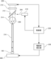
- FIG. 3 is a block diagram showing the configuration of an apparatus used for measurement using the diamond sensor shown in FIG.
- FIG. 4 is a sequence diagram showing the timing of irradiation of excitation light and electromagnetic waves and the timing of measurement of synchrotron radiation during measurement using the diamond spin sensor shown in FIG.
- FIG. 5 is a graph showing a schematic relationship between the observed signal intensity (i.e., the intensity of the emitted light) and the frequency of the electromagnetic wave (i.e., the microwave).
- FIG. 6 is a perspective view showing the measurement of a magnetic field and an electric field using the diamond spin sensor shown in FIG. FIG.
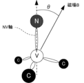
- FIG. 7 is a schematic diagram showing the NV center of diamond.
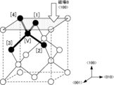
- FIG. 8 is a perspective view showing the relationship between the four possible directions of the NV axis of diamond and the magnetic field in the ⁇ 100> direction.
- FIG. 9 is a graph showing a schematic relationship between the signal intensity and the electromagnetic wave frequency observed in the state shown in FIG.
- FIG. 10 is a perspective view showing the relationship between the four possible directions of the NV axis of diamond and the magnetic field in the ⁇ 110> direction.
- FIG. 11 is a graph showing a schematic relationship between the signal intensity and the electromagnetic wave frequency observed in the state shown in FIG.
- FIG. 12 is a perspective view showing the relationship between the four possible directions of the NV axis of diamond and the magnetic field in the ⁇ 111> direction.
- FIG. 13 is a graph showing a schematic relationship between the signal intensity and the electromagnetic wave frequency observed in the state shown in FIG.
- FIG. 14 is a schematic diagram showing a method for manufacturing a diamond spin sensor.
- FIG. 15 is a schematic diagram showing a method for manufacturing a diamond spin sensor, which is different from that shown in FIG.
- the axis passing through N and V of the NV center formed in diamond can take four directions from the crystal structure of diamond. Since the sensitivity as a sensor depends on the direction of the NV axis relative to the detection target (e.g., magnetic field or electric field), it is preferable to align the NV axis. For example, the NV axis can be aligned in a direction perpendicular to the (111) crystal plane by CVD (Chemical Vapor Deposition). However, since the total number of NV centers is small and the amount of fluorescence is weak, a sufficient S/N ratio cannot be obtained.
- CVD Chemical Vapor Deposition
- the present disclosure therefore aims to provide a diamond spin sensor that has color centers with aligned axes and can improve detection sensitivity, and a method for manufacturing the same.
- a diamond spin sensor includes a diamond substrate and an inclined surface formed on the diamond substrate, in which color centers having electronic spins are formed, and among the color centers formed on the inclined surface, the color centers whose color center axes are perpendicular to the inclined surface are present at a ratio of at least twice as high as the color centers whose color center axes are not perpendicular to the inclined surface. This makes it possible to realize a diamond spin sensor that has multiple color centers with aligned color center axes and can improve detection sensitivity.
- the color center can include an NV - center. This makes it possible to realize a diamond spin sensor having a plurality of NV - centers with aligned axes, thereby improving detection sensitivity.
- the inclined surface may include a first inclined surface and a second inclined surface, the second inclined surface may be disposed on the back surface of the first inclined surface, the first inclined surface may have a (111) crystal plane, and the second inclined surface may have a (-1-11) crystal plane.
- the color centers whose color center axes are perpendicular to the first inclined surface may exist at a ratio of at least twice as many as the color centers whose color center axes are not perpendicular to the first inclined surface
- the color centers whose color center axes are perpendicular to the second inclined surface may exist at a ratio of at least twice as many as the color centers whose color center axes are not perpendicular to the second inclined surface.
- the diamond spin sensor when measuring the electric field formed by the current flowing through a predetermined portion of the conductive wire, the diamond spin sensor may be positioned with respect to the conductive wire so that the predetermined portion is located within a plane defined by the ⁇ 111> direction, which is the normal direction of the first inclined surface, and the ⁇ -1-11> direction, which is the normal direction of the second inclined surface. This allows the electric field formed by the current flowing through the predetermined portion of the conductive wire to be measured with high accuracy.
- a method for manufacturing a diamond spin sensor includes a preparation step of preparing a single crystal diamond substrate having a (001) crystal face on its surface, a crystal face formation step of forming a (111) crystal face and a (-1-11) crystal face on the surface of the substrate, and an NV formation step of forming NV centers on the (111) crystal face and the (-1-11) crystal face by CVD.
- Diamond substrates having a (100) crystal face are easy to obtain in relatively large sizes, making it easy to manufacture diamond spin sensors.
- the method may further include a step of forming a mask of a predetermined width extending along the ⁇ 1-10> direction on the (001) crystal plane, an etching step of etching the (001) crystal plane on which the mask is formed, and a step of removing the mask remaining after etching
- the crystal plane formation step may include a step of performing CVD by setting the substrate at a predetermined temperature in an environment containing methane and hydrogen. This allows color centers to be formed on the (111) crystal plane and (-1-11) crystal plane having a larger area than before, improving detection sensitivity.
- the CVD in the CVD step may be performed so that the ⁇ parameter, which represents the ratio of the growth rate in the ⁇ 100> direction to the growth rate in the ⁇ 111> direction, is 2 or more and 3.5 or less. This allows the formation of (111) crystal planes and (-1-11) crystal planes with larger areas.
- the volume ratio of methane to hydrogen may be 1% or more and 20% or less, and the predetermined temperature may be 600°C or more and 1100°C or less. This allows the formation of (111) crystal planes and (-1-11) crystal planes with larger areas.
- the method may further include a step of forming a mask of a predetermined width extending along the ⁇ 1-10> direction on the (001) crystal plane, an etching step of etching the (001) crystal plane on which the mask is formed, and a step of removing the mask remaining after etching, and the crystal plane formation step may include a step of performing hydrogen plasma etching. This allows color centers to be formed on the (111) crystal plane and the (-1-11) crystal plane having a larger area than before, improving detection sensitivity.
- a diamond spin sensor 100 includes a diamond substrate 102 and a plurality of protrusions 104 formed on the diamond substrate 102.
- the surface 112 is a (001) crystal plane.
- the protrusions 104 include a first inclined surface 106 and a second inclined surface 108 located on the rear surface thereof.
- the first inclined surface 106 is a (111) crystal plane, and the second inclined surface 108 is a (-1-11) crystal plane.
- the protrusions 104 are triangular prisms, with one side of the triangular prism abutting the surface 112.
- the protrusions 104 extend along the ⁇ 1-10> direction indicated by the arrow 114.
- the (001) crystal plane in diamond is the plane defined by points A5, A6, A7, and A8.
- the (111) crystal plane is the plane defined by points A5, A2, and A4.
- the (-1-11) crystal plane is the plane defined by points B2, B4, and A5.
- the ⁇ 1-10> direction is, for example, the direction passing through points A1 and C1.
- the convex portion 104 may extend along the ⁇ 110> direction.
- the first inclined surface 106 is a (1-11) crystal plane
- the second inclined surface 108 is a (-111) crystal plane.
- the ⁇ 110> direction is, for example, a direction passing through points A1 and A3.
- the (1-11) crystal plane is a plane defined by points A5, B4, and A2.
- the (-111) crystal plane is a plane defined by points A5, A4, and B2.
- the first inclined surface 106 and the second inclined surface 108 include NV centers 110 composed of nitrogen N and vacancies V. Many of the multiple NV centers 110 included in the first inclined surface 106 have an axis passing through N and V (hereinafter referred to as the NV axis) that is arranged perpendicular to the first inclined surface 106. Many of the multiple NV centers 110 included in the second inclined surface 108 have an NV axis that is arranged perpendicular to the second inclined surface 108.
- the position of N substituting for C in a diamond single crystal can take four positions relative to V. Therefore, the NV axis can take four directions.
- many of the NV centers included in the first inclined surface 106 and the second inclined surface 108 have their NV axes arranged perpendicular to each surface.
- the number of NV centers whose NV axes are arranged perpendicular to each surface depends on the manufacturing process. For example, it is preferable that the ratio of the number of NV centers whose NV axes are arranged perpendicular to each surface is approximately twice or more the number of NV centers whose NV axes point in the other three directions. This makes it possible to realize a diamond spin sensor 100 that has multiple NV centers with aligned NV axes and can improve detection sensitivity.
- the control unit 230 includes a CPU (Central Processing Unit) and a memory unit (neither shown). The processing performed by the control unit 230, which will be described later, is realized by the CPU reading and executing a program previously stored in the memory unit.
- CPU Central Processing Unit
- the excitation light generating unit 210 generates excitation light for exciting the NV center of the diamond spin sensor 100 under the control of the control unit 230.
- the control unit 230 supplies a voltage to the excitation light generating unit 210 at a predetermined timing to cause the excitation light generating unit 210 to emit light.
- the excitation light 204 is green light (i.e., wavelength 490 to 560 nm).
- the excitation light 204 is preferably laser light, and the excitation light generating unit 210 is preferably a semiconductor laser (e.g., emitted light wavelength 532 nm).
- the filter 212 is an element for separating the excitation light 204 incident from the excitation light generating unit 210 and the light (i.e., fluorescent light) emitted from the diamond spin sensor 100, as described below.
- the filter 212 is a filter that cuts out (i.e., reflects) light with wavelengths equal to or less than a predetermined wavelength and passes light with wavelengths greater than the predetermined wavelength, or a bandpass filter that passes light with wavelengths within a predetermined wavelength range and cuts out (i.e., reflects) light with wavelengths outside the predetermined wavelength range.
- excitation light has a shorter wavelength than fluorescent light, so such a configuration is preferable.
- the filter 212 is preferably a dichroic mirror with this function.
- the focusing element 214 focuses the excitation light 204 input from the filter 212.
- the focusing element 214 is, for example, a ball lens.
- the focusing element 214 inputs as much of the excitation light diffused and output from the excitation light generating unit 210 as possible to the end of the optical waveguide 216.
- the optical waveguide 216 includes a medium for transmitting light and transmits light in both directions. That is, the optical waveguide 216 has a first end and a second end, and transmits the excitation light 204 incident on the first end to the second end located near the diamond spin sensor 100.
- the optical waveguide 216 also transmits the emitted light (i.e., fluorescence) from the diamond spin sensor 100 incident on the second end to the first end and outputs it.
- the optical waveguide 216 is, for example, an optical fiber.
- the electromagnetic wave irradiation unit 202 irradiates the diamond spin sensor 100 with electromagnetic waves (e.g., microwaves).
- the electromagnetic wave irradiation unit 202 is, for example, a coil formed including an electrical conductor.
- the electromagnetic waves are supplied from the electromagnetic wave generation unit 232 to the electromagnetic wave irradiation unit 202, for example, via a coaxial cable.
- the irradiation of the excitation light and electromagnetic waves to the diamond spin sensor 100 is controlled by the control unit 230, and is performed, for example, at the timing shown in FIG. 4.
- the control unit 230 controls the excitation light generating unit 210 to output excitation light for a predetermined time (e.g., period t1) at a predetermined timing.
- the control unit 230 controls the electromagnetic wave generating unit 232 to output electromagnetic waves at a predetermined time (e.g., period t2) and a predetermined timing. Any suitable pulse sequence may be used during period t2. This allows the diamond to be irradiated with a temporally and spatially combined electromagnetic wave together with the excitation light.
- the control unit 230 takes in the output signal of the light detecting unit 220 at a predetermined timing (e.g., within period t3) and stores it in the memory unit, as described below.
- the NV center transitions from the ground state to an excited state by green light with a wavelength of 490 nm to 560 nm (e.g., 532 nm laser light), and returns to the ground state by emitting red light with a wavelength of 630 nm to 800 nm (e.g., 637 nm fluorescence).
- the NV center captures one electron (i.e., NV - )
- the control unit 230 controls the excitation light generating unit 210 and the electromagnetic wave generating unit 232 to measure a spectrum such as that shown in FIG. 5. The distance ⁇ f between the two observed valleys depends on the magnetic field strength at the position of the diamond spin sensor 100. The control unit 230 can calculate the magnetic field from ⁇ f.
- the LPF (Long Pass Filter) 218 is a long pass filter that passes light with a wavelength equal to or greater than a predetermined wavelength and cuts (e.g., reflects) light with a wavelength shorter than the predetermined wavelength.
- the fluorescence 206 which is the emitted light of the diamond spin sensor 100, is red light and passes through the LPF 218, but the excitation light 204 output from the excitation light generating unit 210 has a shorter wavelength and does not pass through the LPF 218. This prevents the excitation light 204 emitted from the excitation light generating unit 210 from being detected by the light detecting unit 220 and becoming noise, which reduces the detection sensitivity of the fluorescence 206, which is the emitted light of the diamond spin sensor 100.
- the light detecting unit 220 generates and outputs an electrical signal corresponding to the incident light.
- the light detecting unit 220 is, for example, a photodiode.
- the output signal of the light detecting unit 220 is acquired by the
- the magnetic field can be calculated from changes in the ESR spectrum, but it is known that the resonance frequency of the NV center has temperature dependence in the range from 120 K to 700 K.
- the resonance frequency of the NV center has temperature dependence in the range from 120 K to 700 K.
- the diamond spin sensor 100 when used to measure an electric field generated by a current, the diamond spin sensor 100 is positioned so that the extension direction of the convex portion 104 is perpendicular to the conductive line 300, which is a predetermined portion of the conductive line through which the current flows.
- the predetermined portion is not limited to a portion of the conductive line, but may be the entire conductive line.
- the first sloping surface 106 and the second sloping surface 108 are respectively a (111) crystal plane and a (-1-11) crystal plane, and the diamond spin sensor 100 is positioned so that the conductive line 300 is located within a plane defined by the ⁇ 111> direction and the ⁇ -1-11> direction which are perpendicular to these crystal planes.
- a plane defined by two directions means a plane that includes these two directions.
- the NV centers 110 present on each of the first and second slopes 106 and 108 of the convex portion 104 have their NV axes aligned perpendicular to each surface, and there are two directions in which the NV axes are aligned on the convex portion 104.
- the first slope 106 is a (111) crystal plane, and the NV axes of the NV centers formed on the first slope 106 are aligned in the ⁇ 111> direction, which is perpendicular to the first slope 106.
- the second slope 108 is a (-1-11) crystal plane, and the NV axes of the NV centers formed on the second slope 108 are aligned in the ⁇ -1-11> direction, which is perpendicular to the second slope 108.
- the current flowing through the conductive wire 300 forms a magnetic field vector around the conductive wire 300 in the tangential direction of a concentric circle centered on the conductive wire 300, and the magnetic field vector formed at a position within the plane 302 is perpendicular to the plane 302.
- the magnetic field detected by the NV center has a component in the NV axis direction. That is, the diamond spin sensor 100 detects a change in signal intensity (i.e., fluorescence intensity) according to Bcos ⁇ , where ⁇ is the angle between the magnetic field vector B and the NV axis.
- the NV center can detect components perpendicular to the NV axis.
- the electric field formed on the plane 302 has a component perpendicular to the NV axis. Therefore, the electric field can be detected by the diamond spin sensor 100 (i.e., the NV center 110).
- the diamond spin sensor 100 can measure the electric field without being affected by the magnetic field.
- the diamond spin sensor 100 when measuring temperature, as shown in FIG. 6, by placing the diamond spin sensor 100 relative to the conductive wire 300, the diamond spin sensor 100 (i.e., the NV center 110) can measure the temperature around the conductive wire 300 without being affected by the magnetic field formed by the current flowing through the conductive wire 300. Therefore, if the magnetic field direction is known or can be predicted in advance, the diamond spin sensor 100 can be placed so that the extension direction of its convex portion 104 is perpendicular to the magnetic field and the temperature is measured, allowing accurate measurement without being affected by the magnetic field.
- the ratio of the number of NV centers whose NV axes are arranged perpendicular to each of the first inclined surface 106 and the second inclined surface 108 is approximately twice or more the number of NV centers whose NV axes are oriented in the other three directions. This ratio can be evaluated by measurement.
- Figures 8 to 13 it will be explained that the distribution of the NV axes of the NV centers arranged on the convex portion 104 and the first inclined surface 106 of the diamond spin sensor 100 can be estimated by changing the direction of the magnetic field applied from outside to the diamond spin sensor 100, performing ODMR, and observing the detected signal.
- Figure 8 shows the state in which a magnetic field B is applied in the ⁇ 100> direction in the crystal structure of diamond.
- the crystal axis is shown in the lower right.
- [V] in quotation marks represents a vacancy
- the numbers [1] to [4] in quotation marks represent the four positions where nitrogen (N) can be located relative to [V].
- N nitrogen
- the same magnetic field strength is detected by the NV sensors where N is in each position from [1] to [4], so the frequency proportional to the magnetic field strength (i.e., the distance between the two valleys) is equal.
- Figure 10 shows the state where a magnetic field B is applied in the ⁇ 110> direction in the crystal structure of diamond.
- the crystal axes are the same as in Figure 8.
- a graph including three valleys as shown in Figure 11 is obtained. This is because the angles ⁇ between the NV axis and the magnetic field B in the ⁇ 110> direction when N is at each position from [1] to [4] are 35.3 degrees, 90.0 degrees, 35.3 degrees, and 90.0 degrees, respectively.
- ⁇ is either 35.3 degrees or 90.0 degrees.
- two types of magnetic field strength are detected by the NV sensors with N at each position from [1] to [4], and therefore two types of frequencies proportional to the magnetic field strength (i.e., the distance between the two valleys) are detected.
- Figure 12 shows the state where a magnetic field B is applied in the ⁇ 111> direction in the crystal structure of diamond.
- the crystal axes are the same as in Figure 8.
- a graph including four valleys as shown in Figure 13 is obtained.
- the angles ⁇ between the NV axis and the magnetic field B in the ⁇ 111> direction when N is at each position from [1] to [4] are 0.0 degrees, 70.5 degrees, 70.5 degrees, and 70.5 degrees, respectively.
- ⁇ is either 0.0 degrees or 70.5 degrees.
- the magnitude of the valley drop (i.e., signal strength) shown in Figures 9, 11, and 13 corresponds to the intensity of the fluorescence emitted from the NV center, and depends on the proportion of the directions of the four NV axes of the diamond. Therefore, by performing ODMR while changing the direction of the magnetic field applied to the diamond crystal structure, the proportion of the NV axis directions can be calculated from the observed valley (specifically, the degree of drop).
- a diamond substrate 500 of a predetermined size is prepared. Specifically, a type Ib diamond single crystal synthesized by the high-pressure high-temperature (HPHT) method is cut and polished by a laser so that the (001) plane becomes the main surface. Furthermore, the diamond substrate 500 is prepared by cleaning using a mixture of concentrated sulfuric acid and concentrated nitric acid. Diamonds are classified according to the presence or absence of impurities and the type of impurity. Type Ib diamond contains nitrogen atoms as impurities (i.e., has an NV center).
- HPHT high-pressure high-temperature
- step (B) an aluminum (Al) film is formed on the surface (i.e., the (001) surface) of the diamond substrate 500, for example, by sputtering, a pattern is formed by photolithography, and a rectangular mask 502 (i.e., an Al mask) is formed by etching using buffered hydrofluoric acid.
- the mask 502 is formed, for example, so as to extend in the ⁇ 1-10> direction relative to the diamond crystal.
- the dimensions of the mask 502 are, for example, 3 ⁇ m in width and 100 ⁇ m in length. Multiple masks 502 may be formed in parallel.
- Ten masks 502 may be formed, spaced apart from each other by, for example, 10 ⁇ m.
- the mask 502 may be formed so as to extend in the ⁇ 110> direction relative to the diamond crystal.
- step (C) the diamond substrate 500 is etched by dry etching using the RIE (Reactive Ion Etching) method to form a wall surface along the rectangular mask 502.
- a mixed gas of carbon tetrafluoride (CF 4 ) and oxygen (O 2 ) can be used for the gas used in the dry etching.
- the pressure of the mixed gas is, for example, 1 Pa.
- the RF power is, for example, 300 W, and the dry etching is performed for, for example, 1 hour.
- the mask 502 remaining after the dry etching is removed.
- the diamond substrate 500 is etched by the CF 4 cations 504.
- the diamond substrate 500a shows the diamond substrate 500 as a result of etching.
- the etching conditions are not limited to the above.
- step (D) the diamond substrate 500a formed in step (C) is placed in a microwave plasma CVD apparatus and (001) oriented growth is performed.
- a first slope 506 having a long (111) crystal face and a second slope 508 having a (-1-11) crystal face on the back side of the first slope 506 are formed along the wall surface formed in step (C).
- CH 4 methane
- H 2 hydrogen
- a pressure of 100 Torr about 13.3 kPa
- microwave power of 2 kW a substrate temperature of 800°C.
- a first inclined surface 506 having a (111) crystal face and a second inclined surface 508 having a (-1-11) crystal face are formed.
- a first inclined surface 506 having a (1-11) crystal face and a second inclined surface 508 having a (-111) crystal face are formed.
- step (E) (111) oriented growth is performed in a microwave plasma CVD apparatus while adding nitrogen (N), to form a first NV layer 510 and a second NV layer 512 having oriented NV centers on the surface of the first slant surface 506 (i.e., the (111) crystal plane) and the second slant surface 508 (i.e., the (-1-11) crystal plane), respectively. That is, in the first NV layer 510, an NV center having an NV axis perpendicular to the surface of the first NV layer 510 is formed. In the second NV layer 512, an NV center having an NV axis perpendicular to the surface of the second NV layer 512 is formed.
- the CVD conditions for forming an NV center having an NV axis perpendicular to the surface are not limited to the above.
- a diamond spin sensor 100 can be manufactured that has multiple NV centers with aligned NV axes, enabling the detection sensitivity to be improved.
- Diamond substrates with a (100) crystal face are easy to obtain in relatively large sizes, making it easy to manufacture diamond spin sensors.
- the first manufacturing method of the diamond spin sensor includes, between step (A) and the crystal plane formation step (D), step (B) of forming a mask 502 of a predetermined width extending along the ⁇ 110> direction on the (001) crystal plane. It also includes an etching step of etching the (001) crystal plane on which the mask 502 is formed, and a step (C) of removing the mask 502 remaining after etching, and the crystal plane formation step (D) includes a step of performing CVD in an environment containing methane and hydrogen at a predetermined temperature. This allows NV centers to be formed on the (111) crystal plane and (-1-11) crystal plane with a larger area than before, improving the detection sensitivity of the diamond spin sensor.
- step (D) the CVD growth condition is set such that the ⁇ parameter, which represents the ratio of the growth rates in the ⁇ 100> and ⁇ 111> directions, is ⁇ 2, thereby forming a surface oriented to the (111) and ( ⁇ 1-11) planes.
- the ⁇ parameter is defined by the following equation, where the growth rate in the ⁇ 100> direction (i.e., the direction perpendicular to the (100) plane) is V 100 and the growth rate in the ⁇ 111> direction (i.e., the direction perpendicular to the (111) plane) is V 111 .
- the volume ratio of methane to hydrogen is not limited to the above value, and may be 1% or more and 20% or less.
- the substrate temperature is not limited to the above value, and may be 600°C or more and 1100°C or less. This allows the formation of (111) crystal planes and (-1-11) crystal planes with larger areas.
- the diamond spin sensor manufactured as described above can be used to measure the temperature of a sample in an environment where a magnetic field is present by placing the diamond spin sensor in a direction perpendicular to the NV axis and performing ODMR measurement.
- the diamond spin sensor 100 is brought into contact with the sample to equalize the temperatures of both, and in the configuration shown in FIG. 3, the electromagnetic wave irradiation unit 202 irradiates the diamond spin sensor 100 with electromagnetic waves (e.g., microwaves).
- the electromagnetic wave irradiation unit 202 may use, for example, a coil formed with an electric conductor, or a resonator such as a ⁇ /4 open stub made of copper foil and ceramic, and irradiate microwaves with an intensity of, for example, 0.5 mW or more.
- the excitation light output from the light-emitting element may be irradiated to the diamond spin sensor 100 through an optical waveguide 216 such as an optical fiber with an intensity of, for example, 0.1 mW or more.
- the diamond spin sensor shown in Fig. 1 may be manufactured using a method other than the manufacturing method shown in Fig. 14.
- the manufacturing method shown in Fig. 15 may be used.
- the manufacturing method shown in Fig. 15 includes the same processes as the manufacturing method shown in Fig. 14. Therefore, the following description will not be repeated and will focus mainly on the differences.
- step (A) a diamond substrate 500 of a predetermined size is prepared in the same manner as in step (A) of FIG. 14.
- step (B) an aluminum (Al) film is formed on the surface (i.e., the (001) surface) of the diamond substrate 500 in the same manner as in step (B) of FIG. 14, a pattern is formed by photolithography, and a rectangular mask 520 (i.e., an Al mask) is formed by etching.
- the mask 520 is formed so as to extend in the ⁇ 110> direction with respect to the diamond crystal. However, the mask 520 is wider than the mask 502 in FIG. 14.
- the width of the mask 520 is, for example, 4 ⁇ m.
- a plurality of masks 520 may be formed in parallel. Ten masks 520 may be formed, spaced apart from each other by, for example, 10 ⁇ m.
- step (C) similar to step (C) of FIG. 14, the diamond substrate 500 is etched by dry etching using the RIE method to form a wall surface along the rectangular mask 520.
- the mask 520 remaining after the dry etching is removed.
- step (D) the diamond substrate 500a formed in step (C) is placed in a microwave plasma CVD device and anisotropic etching (e.g., plasma etching) is performed.
- anisotropic etching e.g., plasma etching
- This forms a first slope 522 with a long (111) crystal face along the wall surface formed in step (C), and a second slope 524 with a (-1-11) crystal face on the back surface of the first slope 522.
- anisotropic etching i.e., hydrogen plasma etching
- anisotropic etching is performed using a single hydrogen gas (concentration 100%) at a pressure of 80 Torr (approximately 10.7 kPa), a microwave power of 3 kW, and a substrate temperature of 950°C.
- step (E) similar to step (E) of FIG. 14, (111) oriented growth is performed in a microwave plasma CVD apparatus while adding nitrogen (N).
- N nitrogen
- An NV center having an NV axis perpendicular to the surface of the second NV layer 528 is formed in the second NV layer 528.
- a diamond spin sensor 100 can be manufactured that has multiple NV centers with aligned NV axes, enabling the detection sensitivity to be improved.
- Diamond substrates with a (100) crystal face are easy to obtain in relatively large sizes, making it easy to manufacture diamond spin sensors.
- the second manufacturing method for diamond spin sensors includes, between step (A) and the crystal plane formation step (D), step (B) of forming a mask 520 of a predetermined width extending along the ⁇ 110> direction on the (001) crystal plane. It also includes an etching step of etching the (001) crystal plane on which the mask 520 is formed, and a step (C) of removing the mask 520 remaining after etching, and the crystal plane formation step (D) includes a step of performing hydrogen plasma etching. This allows NV centers to be formed on the (111) crystal plane and (-1-11) crystal plane with a larger area than conventional methods, improving the detection sensitivity of the diamond spin sensor.
- the diamond has been described as having an NV center, but this is not limiting. Any diamond having a color center with electronic spin may be used.
- a color center with electronic spin is a center that forms a spin triplet state and emits light when excited, and the NV center is a representative example.
- color centers with electronic spin also exist in silicon-vacancy centers (i.e., Si-V centers), germanium-vacancy centers (i.e., Ge-V centers), and tin-vacancy centers (i.e., Sn-V centers). Therefore, a diamond spin sensor may be constructed using a diamond that contains any of these. This makes it possible to realize a diamond spin sensor that has multiple color centers with aligned color center axes and can improve detection sensitivity.
- the diamond spin sensor manufactured as described above can be used to measure the electric field applied to a sample in an environment where an AC magnetic field and an AC electric field are present, by placing the diamond spin sensor in a direction perpendicular to the NV axis and performing electric field measurements using a pulse sequence.
- a free induction decay (FID) signal can be used as the magnetic resonance signal.
- the diamond spin sensor 100 is placed near or inside the sample, and the electromagnetic wave irradiation unit 202 irradiates the diamond spin sensor 100 with electromagnetic waves (e.g., microwaves).
- a coil formed with an electric conductor, or a resonator such as a ⁇ /4 open stub made of copper foil and ceramic, can be used, and microwaves with an intensity of, for example, 0.5 mW or more can be irradiated.
- the excitation light output from the light-emitting element can be irradiated to the diamond spin sensor 100 with an intensity of, for example, 0.1 mW or more through an optical waveguide 216 such as an optical fiber.
Landscapes
- Chemical & Material Sciences (AREA)
- Physics & Mathematics (AREA)
- Engineering & Computer Science (AREA)
- Organic Chemistry (AREA)
- Metallurgy (AREA)
- Materials Engineering (AREA)
- Crystallography & Structural Chemistry (AREA)
- General Chemical & Material Sciences (AREA)
- Chemical Kinetics & Catalysis (AREA)
- General Physics & Mathematics (AREA)
- Condensed Matter Physics & Semiconductors (AREA)
- Electromagnetism (AREA)
- Crystals, And After-Treatments Of Crystals (AREA)
Priority Applications (3)
| Application Number | Priority Date | Filing Date | Title |
|---|---|---|---|
| JP2025515059A JPWO2024219050A1 (https=) | 2023-04-18 | 2024-02-02 | |
| CN202480026238.3A CN121039516A (zh) | 2023-04-18 | 2024-02-02 | 金刚石自旋传感器及其制造方法 |
| EP24792326.1A EP4700418A1 (en) | 2023-04-18 | 2024-02-02 | Diamond spin sensor and method for manufacturing same |
Applications Claiming Priority (2)
| Application Number | Priority Date | Filing Date | Title |
|---|---|---|---|
| JP2023-067532 | 2023-04-18 | ||
| JP2023067532 | 2023-04-18 |
Publications (1)
| Publication Number | Publication Date |
|---|---|
| WO2024219050A1 true WO2024219050A1 (ja) | 2024-10-24 |
Family
ID=93152264
Family Applications (1)
| Application Number | Title | Priority Date | Filing Date |
|---|---|---|---|
| PCT/JP2024/003395 Ceased WO2024219050A1 (ja) | 2023-04-18 | 2024-02-02 | ダイヤモンドスピンセンサおよびその製造方法 |
Country Status (4)
| Country | Link |
|---|---|
| EP (1) | EP4700418A1 (https=) |
| JP (1) | JPWO2024219050A1 (https=) |
| CN (1) | CN121039516A (https=) |
| WO (1) | WO2024219050A1 (https=) |
Cited By (1)
| Publication number | Priority date | Publication date | Assignee | Title |
|---|---|---|---|---|
| WO2025182849A1 (ja) * | 2024-02-28 | 2025-09-04 | 住友電気工業株式会社 | ダイヤモンドセンサ |
Citations (9)
| Publication number | Priority date | Publication date | Assignee | Title |
|---|---|---|---|---|
| JP2009518273A (ja) * | 2005-12-09 | 2009-05-07 | エレメント シックス テクノロジーズ (プロプライアタリー) リミテッド | 高結晶品質の合成ダイヤモンド |
| WO2015107907A1 (ja) * | 2014-01-20 | 2015-07-23 | 独立行政法人科学技術振興機構 | ダイヤモンド結晶、ダイヤモンド素子、磁気センサー、磁気計測装置、および、センサーアレイの製造方法 |
| CN107356820A (zh) * | 2017-06-07 | 2017-11-17 | 南京邮电大学 | 一种基于脉冲光探测磁共振的电磁场近场成像系统及方法 |
| JP2020063960A (ja) * | 2018-10-16 | 2020-04-23 | 国立大学法人東京工業大学 | 磁気計測装置 |
| US20210149004A1 (en) * | 2018-04-30 | 2021-05-20 | Maxim Khodas | Estimation of dynamical properties of fluids using optical defects in solids |
| US20210172739A1 (en) * | 2019-12-06 | 2021-06-10 | Robert Bosch Gmbh | Method for Ascertaining the Change in a Spatial Orientation of an NMR Gyroscope and an NMR Gyroscope |
| JP2021193377A (ja) * | 2018-03-09 | 2021-12-23 | ソマロジック, インコーポレイテッドSomaLogic, Inc. | 量子センサーを使用したプロテオームアッセイ |
| WO2022210936A1 (ja) * | 2021-03-31 | 2022-10-06 | 住友電気工業株式会社 | 単結晶ダイヤモンド及びその製造方法 |
| JP2023067532A (ja) | 2021-11-01 | 2023-05-16 | 三菱電機株式会社 | 乾燥装置、熱交換換気装置および乾燥制御方法 |
-
2024
- 2024-02-02 CN CN202480026238.3A patent/CN121039516A/zh active Pending
- 2024-02-02 EP EP24792326.1A patent/EP4700418A1/en active Pending
- 2024-02-02 JP JP2025515059A patent/JPWO2024219050A1/ja active Pending
- 2024-02-02 WO PCT/JP2024/003395 patent/WO2024219050A1/ja not_active Ceased
Patent Citations (9)
| Publication number | Priority date | Publication date | Assignee | Title |
|---|---|---|---|---|
| JP2009518273A (ja) * | 2005-12-09 | 2009-05-07 | エレメント シックス テクノロジーズ (プロプライアタリー) リミテッド | 高結晶品質の合成ダイヤモンド |
| WO2015107907A1 (ja) * | 2014-01-20 | 2015-07-23 | 独立行政法人科学技術振興機構 | ダイヤモンド結晶、ダイヤモンド素子、磁気センサー、磁気計測装置、および、センサーアレイの製造方法 |
| CN107356820A (zh) * | 2017-06-07 | 2017-11-17 | 南京邮电大学 | 一种基于脉冲光探测磁共振的电磁场近场成像系统及方法 |
| JP2021193377A (ja) * | 2018-03-09 | 2021-12-23 | ソマロジック, インコーポレイテッドSomaLogic, Inc. | 量子センサーを使用したプロテオームアッセイ |
| US20210149004A1 (en) * | 2018-04-30 | 2021-05-20 | Maxim Khodas | Estimation of dynamical properties of fluids using optical defects in solids |
| JP2020063960A (ja) * | 2018-10-16 | 2020-04-23 | 国立大学法人東京工業大学 | 磁気計測装置 |
| US20210172739A1 (en) * | 2019-12-06 | 2021-06-10 | Robert Bosch Gmbh | Method for Ascertaining the Change in a Spatial Orientation of an NMR Gyroscope and an NMR Gyroscope |
| WO2022210936A1 (ja) * | 2021-03-31 | 2022-10-06 | 住友電気工業株式会社 | 単結晶ダイヤモンド及びその製造方法 |
| JP2023067532A (ja) | 2021-11-01 | 2023-05-16 | 三菱電機株式会社 | 乾燥装置、熱交換換気装置および乾燥制御方法 |
Non-Patent Citations (3)
| Title |
|---|
| M. LESIKJ.-P. TETIENNEA. TALLAIREJ. ACHARDV, MILLEA. GICQUELJ.-F. ROCHV. JACQUES: "Perfect preferential orientation of nitrogen-vacancy defects in a synthetic diamond sample", APPL. PHYS. LETT., vol. 104, 2014, pages 113107 |
| M. W. DOHERTYV. M. ACOSTAA. JARMOLAM. S. J. BARSONN. B. MANSOND. BUDKERL. C. L. HOLLENBERG: "Temperature shifts of the resonances of the NV- center in diamond", PHYSICAL REVIEW B, vol. 90, 2014, pages 041201 |
| YUTA NAKANOSHU INAGAKIKAZUKI KOBAYASHIMORIYOSHI HARUYAMAHIROMITSU KATOCHRISTOPH E. NEBELXUFANG ZHANGTSUBASA MATSUMOTOTAKAO INOKUMA: "Proceedings of the 69th JSAP (the Japan Society of Applied Physics", vol. 25, 2022, SPRING MEETING, article "Development of heavily nitrogen-doped diamond growth with suppression of 2D nucleation", pages: 204 - 1 |
Cited By (1)
| Publication number | Priority date | Publication date | Assignee | Title |
|---|---|---|---|---|
| WO2025182849A1 (ja) * | 2024-02-28 | 2025-09-04 | 住友電気工業株式会社 | ダイヤモンドセンサ |
Also Published As
| Publication number | Publication date |
|---|---|
| CN121039516A (zh) | 2025-11-28 |
| EP4700418A1 (en) | 2026-02-25 |
| JPWO2024219050A1 (https=) | 2024-10-24 |
Similar Documents
| Publication | Publication Date | Title |
|---|---|---|
| JP5571803B2 (ja) | Cvd単結晶ダイヤモンド材料 | |
| US5294289A (en) | Detection of interfaces with atomic resolution during material processing by optical second harmonic generation | |
| US9335606B2 (en) | Device for achieving multi-photon interference from nitrogen-vacancy defects in diamond material | |
| US9385654B2 (en) | High-precision GHZ clock generation using spin states in diamond | |
| US9017633B2 (en) | CVD single crystal diamond material | |
| US20120051996A1 (en) | Diamond material | |
| Boiron et al. | Single molecules of dibenzanthanthrene in n‐hexadecane | |
| Pallmann et al. | Cavity-mediated collective emission from few emitters in a diamond membrane | |
| Çakan et al. | Quantum optics applications of hexagonal boron nitride defects | |
| Jung et al. | Spin measurements of NV centers coupled to a photonic crystal cavity | |
| US20240053208A1 (en) | Apparatus for measuring temperature using diamond nitrogen-vacancy center sensor and manufacturing method therefor | |
| WO2024219050A1 (ja) | ダイヤモンドスピンセンサおよびその製造方法 | |
| Joe et al. | Observation of the acoustic Purcell effect with a color-center and a nanomechanical resonator | |
| US20240210625A1 (en) | Low Temperature Fabrication of Silicon Nitride Photonic Devices | |
| Hönerlage et al. | Exciton polaritons and hyper-Raman scattering in zinc-blende-type semiconductors: CuBr as an example | |
| RU2587468C2 (ru) | Способ измерения плотности электронов в плазме методом оптической спектроскопии | |
| Fukuda et al. | Allan-variance measurements of diode laser frequency-stabilized with a thin vapor cell | |
| Pakulis et al. | Optically detected electron cyclotron resonance in silicon | |
| Stancu et al. | In situ monitoring of silicon plasma etching using a quantum cascade laser arrangement | |
| JP5665042B2 (ja) | 位相保持型ラムゼー法を用いた基準信号発生器および基準信号発生方法 | |
| Noh et al. | Two-photon interference of biphotons emitted by overlapping resonances in metasurfaces | |
| Ahuja et al. | Guided mode resonance-driven photoluminescence enhancement and angular emission control in a 2D dielectric photonic lattice | |
| Lettner | Nanomanipulation of quantum emitter in nanometer-sized solid-state host for quantum optical applications | |
| Antoniuk | Spin-photon interface in hybrid quantum photonics with negatively charged silicon vacancy centers in nanodiamonds | |
| Joe et al. | Purcell-enhanced spin–phonon coupling with a single colour centre |
Legal Events
| Date | Code | Title | Description |
|---|---|---|---|
| 121 | Ep: the epo has been informed by wipo that ep was designated in this application |
Ref document number: 24792326 Country of ref document: EP Kind code of ref document: A1 |
|
| ENP | Entry into the national phase |
Ref document number: 2025515059 Country of ref document: JP Kind code of ref document: A |
|
| WWE | Wipo information: entry into national phase |
Ref document number: 2025515059 Country of ref document: JP |
|
| WWE | Wipo information: entry into national phase |
Ref document number: 2024792326 Country of ref document: EP |
|
| NENP | Non-entry into the national phase |
Ref country code: DE |
|
| ENP | Entry into the national phase |
Ref document number: 2024792326 Country of ref document: EP Effective date: 20251118 |
|
| ENP | Entry into the national phase |
Ref document number: 2024792326 Country of ref document: EP Effective date: 20251118 |
|
| ENP | Entry into the national phase |
Ref document number: 2024792326 Country of ref document: EP Effective date: 20251118 |
|
| ENP | Entry into the national phase |
Ref document number: 2024792326 Country of ref document: EP Effective date: 20251118 |
|
| ENP | Entry into the national phase |
Ref document number: 2024792326 Country of ref document: EP Effective date: 20251118 |
|
| ENP | Entry into the national phase |
Ref document number: 2024792326 Country of ref document: EP Effective date: 20251118 |
|
| ENP | Entry into the national phase |
Ref document number: 2024792326 Country of ref document: EP Effective date: 20251118 |
|
| ENP | Entry into the national phase |
Ref document number: 2024792326 Country of ref document: EP Effective date: 20251118 |
|
| ENP | Entry into the national phase |
Ref document number: 2024792326 Country of ref document: EP Effective date: 20251118 |
|
| WWP | Wipo information: published in national office |
Ref document number: 2024792326 Country of ref document: EP |