WO2024218845A1 - 表示装置 - Google Patents
表示装置 Download PDFInfo
- Publication number
- WO2024218845A1 WO2024218845A1 PCT/JP2023/015420 JP2023015420W WO2024218845A1 WO 2024218845 A1 WO2024218845 A1 WO 2024218845A1 JP 2023015420 W JP2023015420 W JP 2023015420W WO 2024218845 A1 WO2024218845 A1 WO 2024218845A1
- Authority
- WO
- WIPO (PCT)
- Prior art keywords
- pixel circuit
- stage
- signal line
- mode
- data signal
- Prior art date
- Legal status (The legal status is an assumption and is not a legal conclusion. Google has not performed a legal analysis and makes no representation as to the accuracy of the status listed.)
- Ceased
Links
Images




Classifications
-
- G—PHYSICS
- G09—EDUCATION; CRYPTOGRAPHY; DISPLAY; ADVERTISING; SEALS
- G09G—ARRANGEMENTS OR CIRCUITS FOR CONTROL OF INDICATING DEVICES USING STATIC MEANS TO PRESENT VARIABLE INFORMATION
- G09G3/00—Control arrangements or circuits, of interest only in connection with visual indicators other than cathode-ray tubes
- G09G3/20—Control arrangements or circuits, of interest only in connection with visual indicators other than cathode-ray tubes for presentation of an assembly of a number of characters, e.g. a page, by composing the assembly by combination of individual elements arranged in a matrix no fixed position being assigned to or needed to be assigned to the individual characters or partial characters
-
- G—PHYSICS
- G09—EDUCATION; CRYPTOGRAPHY; DISPLAY; ADVERTISING; SEALS
- G09G—ARRANGEMENTS OR CIRCUITS FOR CONTROL OF INDICATING DEVICES USING STATIC MEANS TO PRESENT VARIABLE INFORMATION
- G09G3/00—Control arrangements or circuits, of interest only in connection with visual indicators other than cathode-ray tubes
- G09G3/20—Control arrangements or circuits, of interest only in connection with visual indicators other than cathode-ray tubes for presentation of an assembly of a number of characters, e.g. a page, by composing the assembly by combination of individual elements arranged in a matrix no fixed position being assigned to or needed to be assigned to the individual characters or partial characters
- G09G3/22—Control arrangements or circuits, of interest only in connection with visual indicators other than cathode-ray tubes for presentation of an assembly of a number of characters, e.g. a page, by composing the assembly by combination of individual elements arranged in a matrix no fixed position being assigned to or needed to be assigned to the individual characters or partial characters using controlled light sources
- G09G3/30—Control arrangements or circuits, of interest only in connection with visual indicators other than cathode-ray tubes for presentation of an assembly of a number of characters, e.g. a page, by composing the assembly by combination of individual elements arranged in a matrix no fixed position being assigned to or needed to be assigned to the individual characters or partial characters using controlled light sources using electroluminescent panels
- G09G3/32—Control arrangements or circuits, of interest only in connection with visual indicators other than cathode-ray tubes for presentation of an assembly of a number of characters, e.g. a page, by composing the assembly by combination of individual elements arranged in a matrix no fixed position being assigned to or needed to be assigned to the individual characters or partial characters using controlled light sources using electroluminescent panels semiconductive, e.g. using light-emitting diodes [LED]
- G09G3/3208—Control arrangements or circuits, of interest only in connection with visual indicators other than cathode-ray tubes for presentation of an assembly of a number of characters, e.g. a page, by composing the assembly by combination of individual elements arranged in a matrix no fixed position being assigned to or needed to be assigned to the individual characters or partial characters using controlled light sources using electroluminescent panels semiconductive, e.g. using light-emitting diodes [LED] organic, e.g. using organic light-emitting diodes [OLED]
- G09G3/3225—Control arrangements or circuits, of interest only in connection with visual indicators other than cathode-ray tubes for presentation of an assembly of a number of characters, e.g. a page, by composing the assembly by combination of individual elements arranged in a matrix no fixed position being assigned to or needed to be assigned to the individual characters or partial characters using controlled light sources using electroluminescent panels semiconductive, e.g. using light-emitting diodes [LED] organic, e.g. using organic light-emitting diodes [OLED] using an active matrix
- G09G3/3233—Control arrangements or circuits, of interest only in connection with visual indicators other than cathode-ray tubes for presentation of an assembly of a number of characters, e.g. a page, by composing the assembly by combination of individual elements arranged in a matrix no fixed position being assigned to or needed to be assigned to the individual characters or partial characters using controlled light sources using electroluminescent panels semiconductive, e.g. using light-emitting diodes [LED] organic, e.g. using organic light-emitting diodes [OLED] using an active matrix with pixel circuitry controlling the current through the light-emitting element
Definitions
- This disclosure relates to a display device.
- Patent document 1 discloses a display device equipped with a demultiplexer (DEMUX) to ensure sufficient charging time for data lines during high-speed operation.
- DEMUX demultiplexer
- a display device includes an Mth stage pixel circuit, an mth stage pixel circuit that is a stage after the Mth stage, an Nth stage pixel circuit that is a stage after the mth stage, an nth stage pixel circuit that is a stage after the Nth stage, a first data signal line connecting the Mth stage pixel circuit and the Nth stage pixel circuit, a second data signal line connecting the mth stage pixel circuit and the nth stage pixel circuit, a switch circuit connecting the first data signal line and the second data signal line, a data signal source connecting to the switch circuit, and a control unit that controls the switch circuit so that in a first mode, a data signal is supplied from the data signal source to the Mth stage pixel circuit, the mth stage pixel circuit, the Nth stage pixel circuit, and the nth stage pixel circuit in that order, and in a second mode, a control unit that controls the switch circuit so that a data signal is supplied from the data signal source to the Mth stage pixel circuit, the m
- power consumption in the second mode of a display device equipped with a DEMUX is reduced.
- FIG. 1 is a schematic diagram illustrating a configuration example of a display device according to an embodiment of the present disclosure.
- FIG. 11 is a diagram illustrating an example of signal supply in a first mode according to an embodiment of the present disclosure.
- FIG. 11 is a diagram illustrating an example of signal supply in a second mode according to an embodiment of the present disclosure.
- FIG. 11 is a diagram illustrating an example of signal supply in a second mode according to an embodiment of the present disclosure.
- 2 is a diagram showing a configuration example of a pixel circuit shown in FIG. 1;
- FIG. 11 is a diagram illustrating an example of signal supply in a second mode according to an embodiment of the present disclosure.
- 1A and 1B are diagrams illustrating an example of signal supply in a first mode and a second mode according to an embodiment of the present disclosure.
- FIG. 1 is a schematic diagram showing a configuration example of a display device according to an embodiment of the present disclosure.
- the display device 2 according to the present disclosure includes a display section DA in which a plurality of pixel circuits PC are provided, and a frame section NA located around the display section DA.
- the pixel circuit PC located in the xth row and yth column is referred to as the pixel circuit PC[x, y] with [x, y] added.
- the display device 2 includes an Mth stage pixel circuit PC[M,y], an mth stage pixel circuit PC[m,y] which is a stage subsequent to the Mth stage, an Nth stage pixel circuit PC[N,y] which is a stage subsequent to the mth stage, an nth stage pixel circuit PC[n,y] which is a stage subsequent to the Nth stage, a first data signal line DL1[y] connected to the Mth stage pixel circuit PC[M,y] and the Nth stage pixel circuit PC[N,y], a second data signal line DL2[y] connected to the mth stage pixel circuit PC[m,y] and the nth stage pixel circuit PC[n,y], and a switch circuit SWC[y] connected to the first data signal line DL1[y] and the second data signal line DL2[y].
- the switch circuit SWC is a so-called demultiplexing circuit (DEMUX).
- the switch circuit SWC[y] switches so that the first data signal line DL1[y] and the second data signal line DL2[y] are connected to the data signal source DS in the order of first, first, second, and second.
- the first mode makes it easier to ensure the charging and discharging time of the first data signal line DL1 and the second data signal line DL2 by switching the switch circuit SWC. Therefore, the first mode is suitable for high-speed driving.
- the second mode Compared to the first mode, the second mode requires less switching of the switch circuit SWC and consumes less power to drive the switch circuit SWC[y]. Therefore, the power consumption of the display device 2 in the second mode is reduced.
- the switch circuit SWC[y] may include a first switch transistor ATr connected between the data signal source DS and the first data line DL1[y], and a second switch transistor BTr connected between the data signal source DS and the second data line DL2[y].
- the control unit CC may be connected to the gate terminals of the first switch transistor ATr and the second switch transistor BTr via the first control line ASW and the second control line BSW.
- FIG. 2 is a diagram showing an example of signal supply in a first mode according to an embodiment of the present disclosure.
- a data signal can be supplied in the order of the Mth stage pixel circuit PC[M,y], the mth stage pixel circuit PC[m,y], the Nth stage pixel circuit PC[N,y], and the nth stage pixel circuit PC[n,y].
- the Mth stage, the mth stage, the Nth stage, and the nth stage pixel circuits PC[M,y], PC[m,y], PC[N,y], and PC[n,y] can all be updated in one vertical scanning period.
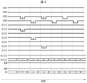
- FIG. 3 and 4 are diagrams showing an example of signal supply in the second mode according to an embodiment of the present disclosure.
- data signals are supplied to the pixel circuits PC[M,y] and PC[N,y] of the Mth and Nth stages, and data signals are not supplied to the pixel circuits PC[m,y] and PC[n,y] of the mth and nth stages.
- FIG. 3 shows that in the second mode, during one of two consecutive vertical scanning periods, data signals are supplied to the pixel circuits PC[M,y] and PC[N,y] of the Mth and Nth stages, and data signals are not supplied to the pixel circuits PC[m,y] and PC[n,y] of the mth and nth stages.
- the display device 2 includes a first shift register circuit SRC1 connected to the Mth stage pixel circuit PC[M,y] and the Nth stage pixel circuit PC[N,y], and a second shift register circuit SRC2 connected to the mth stage pixel circuit PC[m,y] and the nth stage pixel circuit PC[n,y].
- the first shift register circuit SRC1 is connected to the first clock signal line GCK1 and the third clock signal line GCK
- the second shift register circuit SRC2 is connected to the second clock signal line GCK2 and the fourth clock signal line GCK4.
- a clock signal is supplied to the first clock signal line GCK1 and the third clock signal line GCK3 connected to the first shift register circuit SRC1, and a clock signal is supplied to the second clock signal line GCK2 and the fourth clock signal line GCK4 connected to the second shift register circuit SRC2.
- the shift operations of both the first shift register circuit SRC1 and the second shift register circuit SRC2 are performed.
- a constant-level signal is supplied to the second clock signal line GCK2 and the fourth clock signal line GCK4 connected to the second shift register circuit SRC2.
- a constant-level signal is supplied to the first clock signal line GCK1 and the third clock signal line GCK connected to the first shift register circuit SRC1.
- the clock signals supplied in the second mode may be the same as the clock signals supplied in the first mode.
- the vertical scanning period in the first mode and the vertical scanning period in the second mode have the same length.
- the rewrite frequency of the data signal for the same pixel circuit in the first mode is higher than the rewrite frequency of the data signal for the same pixel circuit in the second mode. That is, it is preferable to drive at high speed in the first mode and at low speed in the second mode.
- the first mode may be a so-called video display mode or gaming mode.
- the rewrite frequency of the data signal for the same pixel circuit in the first mode may be 120 Hz or more.
- the rewrite frequency of the data signal for the same pixel circuit in the second mode may be 60 Hz or less.
- the frame rate in the first mode is 240 Hz
- the frame rate in the second mode may be 60 Hz, 30 Hz, 1 Hz, etc.
- the display device 2 includes a plurality of scanning signal lines GL.
- the xth row scanning signal line GL[x] is connected to the xth row pixel circuit PC[x, y] and the unit circuit U[x] in the first shift register circuit SRC1 or the second shift register circuit SRC2.
- FIG. 5 is a diagram showing an example of the configuration of the pixel circuit shown in FIG. 1.
- each pixel circuit PC[x, y] is provided with a drive transistor T4 and a write transistor T3 connected to the first data signal line DL1[y] or the second data signal line DL2[y], and the gate terminal of the write transistor T3 is connected to one of the multiple scanning signal lines GL (scanning signal line GL[x] in FIG. 5).
- Each pixel circuit PC[x,y] may include an internal compensation circuit that compensates for the threshold of the drive transistor T4.
- internal compensation may be performed after a data signal is written.
- the internal compensation circuit includes a compensation transistor T2, and the source or drain terminal of the drive transistor T4 is connected to the gate terminal via the compensation transistor T2.
- Each pixel circuit PC[x,y] may further include an initialization transistor T1, T7, a light-emitting transistor T5, T6, and a storage capacitance Cst.
- Each pixel circuit PC[x,y] may be connected to a light-emitting control line Em[x], a light-emitting element Ed, and wiring that supplies constant potentials ELVdd, ELVss, and Vini.
- the connection with the data signal source DS switches from the first data signal line DL1[y] to the second data signal line DL2[y].
- Changing the potential of the wiring requires charging and discharging, which takes time. With this configuration, the charging and discharging time of the second data signal line DL2[y] can be secured.
- the connection with the data signal source DS switches from the second data signal line DL2[y] to the first data signal line DL1[y]. With this configuration, the charging and discharging time of the first data signal line DL1[y] can be secured.
- the data signal source DS is connected to the first data signal line DL1[y]. Then, while internal compensation is being performed in the first-stage pixel circuit PC[1,y], the connection to the data signal source is switched from the first data signal line DL1[y] to the second data signal line DL2[y]. Then, after the first-stage scanning signal line GL[1] returns from ON to OFF, the connection to the data signal source is switched from the second data signal line DL2[y] to the first data signal line DL1[y].
- the scanning signal line GL[M] connected to the Mth pixel circuit [M,y], the scanning signal line GL[m] connected to the mth pixel circuit PC[m,y], the scanning signal line GL[N] connected to the Nth pixel circuit PC[N,y], and the scanning signal line GL[n] connected to the nth pixel circuit PC[n,y] are selected in this order.
- the scanning signal lines GL are driven in the progressive manner in the first mode.
- the scanning signal line GL[M] connected to the pixel circuit [M,y] of the Mth stage and the scanning signal line GL[N] connected to the pixel circuit PC[N,y] of the Nth stage are selected in this order.
- the scanning signal line GL[m] connected to the pixel circuit PC[m,y] of the mth stage and the scanning signal line GL[n] connected to the pixel circuit PC[n,y] of the nth stage are selected in this order.
- M and N are odd numbers and m and n are even numbers (or when M and N are even numbers and m and n are odd numbers)
- the scanning signal line GL is driven in the interlaced manner in the second mode.
- the display device 2 includes a first driver that drives the scanning signal line GL[M] connected to the pixel circuit [M,y] of the Mth stage and the scanning signal line GL[N] connected to the pixel circuit PC[N,y] of the Nth stage, and a second driver that drives the scanning signal line GL[m] connected to the pixel circuit PC[m,y] of the mth stage and the scanning signal line GL[n] connected to the pixel circuit PC[n,y] of the nth stage, and during each vertical scanning period in the second mode, the operation of one of the first driver and the second driver is stopped.
- the first driver and the second driver operate alternately.
- the first driver is the first shift register circuit SRC1 described above
- the second driver is the second shift register circuit SRC2 described above.
- each pixel circuit PC may be connected to a light-emitting element Ed (see FIG. 5).
- the light-emitting element Ed connected to the Mth stage pixel circuit PC[M,y] and the light-emitting element Ed connected to the Nth stage pixel circuit PC[N,y] may emit the same color
- the light-emitting element Ed connected to the mth stage pixel circuit PC[m,y] and the light-emitting element Ed connected to the nth stage pixel circuit PC[n,y] may emit the same color.
- Each light-emitting element Ed may have an organic light-emitting layer or a quantum dot light-emitting layer.
- FIG. 6 is a diagram showing an example of signal supply in the second mode according to an embodiment of the present disclosure.
- a pause period during which no data signal is supplied to any pixel circuit PC may be provided between two consecutive vertical scanning periods.
- power consumption in the second mode can be further reduced.
- the pause period can be achieved by providing a period during which a constant level signal is supplied to all of the first through fourth clock signal lines GCK1 through GCK4.
- FIG. 7 is a diagram illustrating an example of signal supply in a first mode and a second mode according to an embodiment of the present disclosure.
- the vertical scanning period in the second mode may be longer than the vertical scanning period in the first mode. This configuration can further reduce power consumption in the second mode.
- the extension of the vertical scanning period can be achieved by reducing the clock frequency in the second mode to be lower than the clock frequency in the first mode.
- Embodiment 3 can be combined with embodiment 2 described above.
- the vertical scanning period of the second mode may be longer than the vertical scanning period of the first mode, and a pause period may be provided in the second mode.
Landscapes
- Engineering & Computer Science (AREA)
- Physics & Mathematics (AREA)
- Computer Hardware Design (AREA)
- General Physics & Mathematics (AREA)
- Theoretical Computer Science (AREA)
- Control Of Indicators Other Than Cathode Ray Tubes (AREA)
Priority Applications (2)
| Application Number | Priority Date | Filing Date | Title |
|---|---|---|---|
| PCT/JP2023/015420 WO2024218845A1 (ja) | 2023-04-18 | 2023-04-18 | 表示装置 |
| JP2025514910A JPWO2024218845A1 (https=) | 2023-04-18 | 2023-04-18 |
Applications Claiming Priority (1)
| Application Number | Priority Date | Filing Date | Title |
|---|---|---|---|
| PCT/JP2023/015420 WO2024218845A1 (ja) | 2023-04-18 | 2023-04-18 | 表示装置 |
Publications (1)
| Publication Number | Publication Date |
|---|---|
| WO2024218845A1 true WO2024218845A1 (ja) | 2024-10-24 |
Family
ID=93152415
Family Applications (1)
| Application Number | Title | Priority Date | Filing Date |
|---|---|---|---|
| PCT/JP2023/015420 Ceased WO2024218845A1 (ja) | 2023-04-18 | 2023-04-18 | 表示装置 |
Country Status (2)
| Country | Link |
|---|---|
| JP (1) | JPWO2024218845A1 (https=) |
| WO (1) | WO2024218845A1 (https=) |
Citations (5)
| Publication number | Priority date | Publication date | Assignee | Title |
|---|---|---|---|---|
| JP2006003731A (ja) * | 2004-06-18 | 2006-01-05 | Mitsubishi Electric Corp | 表示装置 |
| JP2006154810A (ja) * | 2004-11-26 | 2006-06-15 | Samsung Sdi Co Ltd | 順次走査及び飛び越し走査兼用の駆動回路及びこれを用いた有機電界発光装置 |
| JP2008083320A (ja) * | 2006-09-27 | 2008-04-10 | Seiko Epson Corp | 電気光学装置、その駆動方法および電子機器 |
| JP2008197626A (ja) * | 2006-12-15 | 2008-08-28 | Nvidia Corp | 節電のためにディスプレイのリフレッシュレートを調整するシステム、方法、及びコンピュータプログラム製品 |
| JP2014219516A (ja) * | 2013-05-07 | 2014-11-20 | 三星ディスプレイ株式會社Samsung Display Co.,Ltd. | 画素回路及びその駆動方法 |
-
2023
- 2023-04-18 JP JP2025514910A patent/JPWO2024218845A1/ja active Pending
- 2023-04-18 WO PCT/JP2023/015420 patent/WO2024218845A1/ja not_active Ceased
Patent Citations (5)
| Publication number | Priority date | Publication date | Assignee | Title |
|---|---|---|---|---|
| JP2006003731A (ja) * | 2004-06-18 | 2006-01-05 | Mitsubishi Electric Corp | 表示装置 |
| JP2006154810A (ja) * | 2004-11-26 | 2006-06-15 | Samsung Sdi Co Ltd | 順次走査及び飛び越し走査兼用の駆動回路及びこれを用いた有機電界発光装置 |
| JP2008083320A (ja) * | 2006-09-27 | 2008-04-10 | Seiko Epson Corp | 電気光学装置、その駆動方法および電子機器 |
| JP2008197626A (ja) * | 2006-12-15 | 2008-08-28 | Nvidia Corp | 節電のためにディスプレイのリフレッシュレートを調整するシステム、方法、及びコンピュータプログラム製品 |
| JP2014219516A (ja) * | 2013-05-07 | 2014-11-20 | 三星ディスプレイ株式會社Samsung Display Co.,Ltd. | 画素回路及びその駆動方法 |
Also Published As
| Publication number | Publication date |
|---|---|
| JPWO2024218845A1 (https=) | 2024-10-24 |
Similar Documents
| Publication | Publication Date | Title |
|---|---|---|
| US10847114B2 (en) | Electro-optical device and electronic device | |
| KR102505897B1 (ko) | Oled 표시패널 | |
| KR100624311B1 (ko) | 프레임 메모리 제어 방법 및 그것을 이용한 표시 장치 | |
| JP4694134B2 (ja) | 表示装置 | |
| KR20080052468A (ko) | 전기 광학 장치, 주사선 구동 회로 및 전자기기 | |
| CN116631325A (zh) | 一种显示面板及其驱动方法、显示装置 | |
| CN114170970B (zh) | 扫描驱动器及包括扫描驱动器的有机发光显示设备 | |
| CN113689824A (zh) | 发射控制驱动器和显示装置 | |
| US7782282B2 (en) | Display device and driving method thereof | |
| CN113948025A (zh) | 显示面板的驱动方法 | |
| KR20190030962A (ko) | 스캔 구동부 및 이를 이용한 표시장치 | |
| CN114765016B (zh) | 包括多路复用器的显示装置 | |
| US10930218B2 (en) | Gate driver for improving luminance and display device including the same | |
| KR20250142279A (ko) | 표시장치 | |
| KR102786532B1 (ko) | 게이트 구동부, 표시장치 및 이의 구동방법 | |
| KR102854036B1 (ko) | 스캔 구동부 및 이를 포함하는 표시장치 | |
| WO2024218845A1 (ja) | 表示装置 | |
| KR102673949B1 (ko) | 게이트 드라이버, 표시장치 및 그의 구동방법 | |
| JPWO2024218845A5 (https=) | ||
| JP4432955B2 (ja) | 表示装置 | |
| US12597388B2 (en) | Display device and driving method thereof | |
| US12424178B2 (en) | Display device | |
| JP2012022187A (ja) | 表示装置 | |
| JP4197852B2 (ja) | アクティブマトリクス型表示装置 | |
| JP4297629B2 (ja) | アクティブマトリクス型表示装置 |
Legal Events
| Date | Code | Title | Description |
|---|---|---|---|
| 121 | Ep: the epo has been informed by wipo that ep was designated in this application |
Ref document number: 23933992 Country of ref document: EP Kind code of ref document: A1 |
|
| ENP | Entry into the national phase |
Ref document number: 2025514910 Country of ref document: JP Kind code of ref document: A |
|
| WWE | Wipo information: entry into national phase |
Ref document number: 2025514910 Country of ref document: JP |
|
| NENP | Non-entry into the national phase |
Ref country code: DE |
|
| 122 | Ep: pct application non-entry in european phase |
Ref document number: 23933992 Country of ref document: EP Kind code of ref document: A1 |