WO2024214701A1 - 回路接続用接着剤フィルム、並びに回路接続構造体及びその製造方法 - Google Patents
回路接続用接着剤フィルム、並びに回路接続構造体及びその製造方法 Download PDFInfo
- Publication number
- WO2024214701A1 WO2024214701A1 PCT/JP2024/014419 JP2024014419W WO2024214701A1 WO 2024214701 A1 WO2024214701 A1 WO 2024214701A1 JP 2024014419 W JP2024014419 W JP 2024014419W WO 2024214701 A1 WO2024214701 A1 WO 2024214701A1
- Authority
- WO
- WIPO (PCT)
- Prior art keywords
- component
- adhesive layer
- circuit connection
- adhesive film
- mass
- Prior art date
- Legal status (The legal status is an assumption and is not a legal conclusion. Google has not performed a legal analysis and makes no representation as to the accuracy of the status listed.)
- Ceased
Links
Images


Classifications
-
- H—ELECTRICITY
- H05—ELECTRIC TECHNIQUES NOT OTHERWISE PROVIDED FOR
- H05K—PRINTED CIRCUITS; CASINGS OR CONSTRUCTIONAL DETAILS OF ELECTRIC APPARATUS; MANUFACTURE OF ASSEMBLAGES OF ELECTRICAL COMPONENTS
- H05K1/00—Printed circuits
- H05K1/02—Details
- H05K1/14—Structural association of two or more printed circuits
- H05K1/144—Stacked arrangements of planar printed circuit boards
-
- C—CHEMISTRY; METALLURGY
- C09—DYES; PAINTS; POLISHES; NATURAL RESINS; ADHESIVES; COMPOSITIONS NOT OTHERWISE PROVIDED FOR; APPLICATIONS OF MATERIALS NOT OTHERWISE PROVIDED FOR
- C09J—ADHESIVES; NON-MECHANICAL ASPECTS OF ADHESIVE PROCESSES IN GENERAL; ADHESIVE PROCESSES NOT PROVIDED FOR ELSEWHERE; USE OF MATERIALS AS ADHESIVES
- C09J163/00—Adhesives based on epoxy resins; Adhesives based on derivatives of epoxy resins
-
- C—CHEMISTRY; METALLURGY
- C09—DYES; PAINTS; POLISHES; NATURAL RESINS; ADHESIVES; COMPOSITIONS NOT OTHERWISE PROVIDED FOR; APPLICATIONS OF MATERIALS NOT OTHERWISE PROVIDED FOR
- C09J—ADHESIVES; NON-MECHANICAL ASPECTS OF ADHESIVE PROCESSES IN GENERAL; ADHESIVE PROCESSES NOT PROVIDED FOR ELSEWHERE; USE OF MATERIALS AS ADHESIVES
- C09J7/00—Adhesives in the form of films or foils
- C09J7/30—Adhesives in the form of films or foils characterised by the adhesive composition
- C09J7/35—Heat-activated
-
- C—CHEMISTRY; METALLURGY
- C09—DYES; PAINTS; POLISHES; NATURAL RESINS; ADHESIVES; COMPOSITIONS NOT OTHERWISE PROVIDED FOR; APPLICATIONS OF MATERIALS NOT OTHERWISE PROVIDED FOR
- C09J—ADHESIVES; NON-MECHANICAL ASPECTS OF ADHESIVE PROCESSES IN GENERAL; ADHESIVE PROCESSES NOT PROVIDED FOR ELSEWHERE; USE OF MATERIALS AS ADHESIVES
- C09J9/00—Adhesives characterised by their physical nature or the effects produced, e.g. glue sticks
- C09J9/02—Electrically-conducting adhesives
-
- H—ELECTRICITY
- H01—ELECTRIC ELEMENTS
- H01R—ELECTRICALLY-CONDUCTIVE CONNECTIONS; STRUCTURAL ASSOCIATIONS OF A PLURALITY OF MUTUALLY-INSULATED ELECTRICAL CONNECTING ELEMENTS; COUPLING DEVICES; CURRENT COLLECTORS
- H01R11/00—Individual connecting elements providing two or more spaced connecting locations for conductive members which are, or may be, thereby interconnected, e.g. end pieces for wires or cables supported by the wire or cable and having means for facilitating electrical connection to some other wire, terminal, or conductive member, blocks of binding posts
- H01R11/01—Individual connecting elements providing two or more spaced connecting locations for conductive members which are, or may be, thereby interconnected, e.g. end pieces for wires or cables supported by the wire or cable and having means for facilitating electrical connection to some other wire, terminal, or conductive member, blocks of binding posts characterised by the form or arrangement of the conductive interconnection between the connecting locations
-
- H—ELECTRICITY
- H05—ELECTRIC TECHNIQUES NOT OTHERWISE PROVIDED FOR
- H05K—PRINTED CIRCUITS; CASINGS OR CONSTRUCTIONAL DETAILS OF ELECTRIC APPARATUS; MANUFACTURE OF ASSEMBLAGES OF ELECTRICAL COMPONENTS
- H05K1/00—Printed circuits
- H05K1/02—Details
- H05K1/14—Structural association of two or more printed circuits
Definitions
- the present invention relates to an adhesive film for circuit connection, a circuit connection structure, and a method for manufacturing the same.
- a glass substrate is used as the substrate, and the circuit materials formed on the glass substrate are metals such as aluminum for the underlayer circuits and ITO (Indium Tin Oxide) for the surface electrodes.
- the circuit materials formed on the glass substrate are metals such as aluminum for the underlayer circuits and ITO (Indium Tin Oxide) for the surface electrodes.
- flexible plastic substrates such as polyimide substrates are used as the substrate, and Ti is mainly used as the circuit material formed on the plastic substrate.
- an adhesive layer and a flexible member such as a polyethylene terephthalate (PET) substrate are usually placed on the underside of the polyimide substrate to provide flexibility (see, for example, Patent Document 1).
- PET polyethylene terephthalate
- COG chip on glass
- various electronic components such as driving ICs are directly mounted on the glass substrate of the display panel.
- COG mounting method for example, a method is used in which a circuit connection structure is obtained by thermocompression bonding a liquid crystal driving IC onto a glass substrate via a circuit connection adhesive film having anisotropic conductivity in which conductive particles are dispersed in the adhesive.
- the main objective of the present invention is to provide an adhesive film for circuit connections that can be used to connect circuit components together, and that can provide a circuit connection structure that has sufficient HAST resistance to stabilize the connection resistance between opposing electrodes.
- thermosetting resin component contains a fluorene skeleton-containing epoxy resin represented by the following general formula (1), and an epoxy resin thermosetting agent.
- R E is a skeletal residue derived from an epoxy resin
- R P is a skeletal residue derived from a phenol compound having a fluorene skeleton
- n represents the number of repeating units.
- This circuit connection adhesive film makes it possible to connect circuit components together and obtain a circuit connection structure that has sufficient HAST resistance in stabilizing the connection resistance between opposing electrodes.
- the reason why such an effect is obtained is not entirely clear, but the inventors speculate as follows:
- the circuit connection adhesive film ensures sufficient fluidity to fill the gaps between the electrodes when connecting the circuit components by thermocompression bonding, and after connection, the rigid structure due to the fluorene skeleton can maintain the elastic modulus of the cured product, thereby improving HAST resistance.
- the fluorene skeleton-containing epoxy resin may have a weight average molecular weight of 5,000 to 8,000.
- the fluorene skeleton-containing epoxy resin may have a softening point of 85 to 105°C.
- the fluorene skeleton-containing epoxy resin has the above molecular weight and/or softening point, it becomes easier to ensure electrical continuity between opposing electrodes of a circuit connection structure, even when circuit components are connected to each other at low pressure.
- the circuit connection adhesive film is made into a reel product, it is possible to improve transferability to circuit components.
- the conductive particles may be unevenly distributed on one side of the film. In this case, it is easier to improve the efficiency of capturing the conductive particles when connecting the circuit.
- an adhesive film for circuit connection comprising a first adhesive layer containing conductive particles, a cured product of a photocurable resin component, and a first thermosetting resin component, and a second adhesive layer provided on the first adhesive layer and containing a second thermosetting resin component, wherein the second thermosetting resin component contains a fluorene skeleton-containing epoxy resin represented by the following general formula (1), and an epoxy resin thermosetting agent:
- R E is a skeletal residue derived from an epoxy resin
- R P is a skeletal residue derived from a phenol compound having a fluorene skeleton
- n represents the number of repeating units.
- This circuit connection adhesive film makes it possible to connect circuit components together and obtain a circuit connection structure that has sufficient HAST resistance to stabilize the connection resistance between opposing electrodes. Furthermore, the above-mentioned circuit connection adhesive film has a first adhesive layer containing conductive particles that contains a cured product of a photocurable resin component, which makes it possible to suppress the flow of conductive particles when connecting circuits, preventing the flowed conductive particles from bridging adjacent circuits and reducing insulation, and further increasing the efficiency of capturing conductive particles.
- the fluorene skeleton-containing epoxy resin may have a weight average molecular weight of 5,000 to 8,000.
- the fluorene skeleton-containing epoxy resin may have a softening point of 85 to 105°C.
- the fluorene skeleton-containing epoxy resin has the above molecular weight and/or softening point, it becomes easier to ensure electrical continuity between opposing electrodes of a circuit connection structure, even when circuit components are connected to each other at low pressure.
- the circuit connection adhesive film is made into a reel product, it is possible to improve transferability to circuit components.
- Another aspect of the present invention provides a method for manufacturing a circuit connection structure, comprising the steps of interposing the above-mentioned circuit connection adhesive film between a first circuit member having a first electrode and a second circuit member having a second electrode, and thermocompressing the first circuit member and the second circuit member to electrically connect the first electrode and the second electrode to each other.
- circuit connection structure comprising a first circuit member having a first electrode, a second circuit member having a second electrode, and a circuit connection portion disposed between the first circuit member and the second circuit member and electrically connecting the first electrode and the second electrode to each other, the circuit connection portion including a cured product of the above-mentioned circuit connection adhesive film.
- the present invention can provide an adhesive film for circuit connection that can be used to connect circuit components together to obtain a circuit connection structure that has sufficient HAST resistance to stabilize the connection resistance between opposing electrodes.
- the present invention can also provide a circuit connection structure that uses the above-mentioned adhesive film for circuit connection, and a method for producing the same.
- FIG. 1 is a schematic cross-sectional view showing one embodiment of an adhesive film for circuit connection.
- FIG. 2 is a schematic cross-sectional view showing one embodiment of a circuit connection structure.
- 3A and 3B are schematic cross-sectional views showing each step of an embodiment of a method for producing a circuit connection structure.
- (meth)acrylate means at least one of acrylate and the corresponding methacrylate.
- the materials exemplified below may be used alone or in combination of two or more.
- the content of each component in the composition means the total amount of the multiple substances present in the composition, unless otherwise specified.
- a numerical range indicated using “ ⁇ ” indicates a range that includes the numerical values written before and after " ⁇ " as the minimum and maximum values, respectively.
- “A or B” means that either A or B may be included, and may also include both.
- Room temperature means 25°C.
- the upper or lower limit of a certain numerical range may be replaced with the upper or lower limit of another numerical range.
- the upper or lower limit of the numerical range may be replaced with a value shown in the examples.
- the adhesive film for circuit connection of the present embodiment contains a thermosetting resin component and conductive particles, and the thermosetting resin component contains a fluorene skeleton-containing epoxy resin represented by the following general formula (1) (hereinafter, also referred to as a (C-F) component), and an epoxy resin thermosetting agent.
- a thermosetting resin component contains a fluorene skeleton-containing epoxy resin represented by the following general formula (1) (hereinafter, also referred to as a (C-F) component), and an epoxy resin thermosetting agent.
- R E is a skeletal residue derived from an epoxy resin
- R P is a skeletal residue derived from a phenol compound having a fluorene skeleton
- n represents the number of repeating units.
- the conductive particles may be unevenly distributed on one side of the film.
- the circuit connection adhesive film may include a region P in the thickness direction of the film that contains a thermosetting resin component and a cured product of a photocurable resin component, and the conductive particles may be dispersed in the region P (the conductive particles may be arranged at intervals in the direction in which the film spreads).
- the circuit connection adhesive film may also have a region S that is provided adjacent to the region P and contains a thermosetting resin component that contains a (C-F) component and an epoxy resin thermosetting agent. Region S may not contain a cured product of a photocurable resin component or conductive particles.
- the (C-F) component can contain a bisphenol fluorene skeleton represented by the following general formula (2).
- R 1 , R 2 , R 3 and R 4 each independently represent a hydrogen atom or a hydrocarbon group having 1 to 8 carbon atoms, which may contain a cyclic structure.
- the content of the above skeleton may be 15 to 70 mol%, 30 to 70 mol%, 20 to 60 mol%, or 30 to 50 mol%.
- This content can be calculated as the mole percent of the total of R P and R E having a bisphenolfluorene skeleton relative to the total of R P and R E in the general formula (1). It can also be calculated from the types and amounts of raw materials used in producing the (C-F) component.
- the epoxy equivalent of the (C-F) component may be 700 to 1500 g/eq, 750 to 1400 g/eq, 800 to 1200 g/eq, or 900 to 1100 g/eq.
- the epoxy equivalent is the number of grams (g/eq) of resin containing 1 gram equivalent of epoxy groups, and is measured according to the method specified in JIS K-7236.
- the (C-F) component may have a weight average molecular weight of 5,000 to 8,000 from the viewpoint of obtaining HAST resistance even in low pressure mounting and from the viewpoint of transferability.
- the weight average molecular weight of the fluorene skeleton-containing epoxy resin means a weight average molecular weight measured by gel permeation chromatography (GPC) under the following conditions.
- Detector Hitachi High-Tech Science L-2490-RI
- Column Gelpack GL-R440+R450+R400M
- Flow rate 2.05ml/min Concentration: 5mg/ml
- Injection volume 200 ⁇ l
- Eluent THF Standard sample: polystyrene
- the (C-F) component may also have a softening point of 100 to 150°C from the standpoint of obtaining HAST resistance even in low-pressure mounting and from the standpoint of transferability.
- the softening point of the fluorene skeleton-containing epoxy resin means a softening point measured under the following conditions using a thermomechanical analyzer (TMA).
- TMA thermomechanical analyzer
- Component (C-F) can be produced by reacting a phenolic compound with a bifunctional epoxy resin in the presence of a catalyst (see, for example, JP 2015-178592 A).
- the phenol compound used as the raw material may include a fluorene skeleton-containing phenol compound represented by the following general formula (3) (hereinafter, also referred to as "phenol compound 3").
- the phenol compound used as the raw material may include other phenol compounds other than phenol compound 3.
- R 11 , R 12 , R 13 , R 14 and R 15 each independently represent a hydrogen atom or a hydrocarbon group having 1 to 8 carbon atoms, which may contain a cyclic structure.
- the main component of the phenol compound 3 may be a compound in which m in general formula (3) is 0 (hereinafter also referred to as "compound 3-a”), and may contain a minor component in which m is 1 or more.
- compound 3-a is 9,9-bis(4-hydroxyphenyl)fluorene (BPFL).
- the content of compound 3-a in phenol compound 3 may be 50% by mass or more.
- the content of the compound in which m is 1 or 2 in phenol compound 3 (hereinafter also referred to as "compound 3-b") may be 0.01 to 1.0 area%, 0.05 to 0.7 area%, or 0.07 to 0.5 area%, when quantified in area% based on the absorption at a wavelength of 272 nm by HPLC measurement.
- R 11 , R 12 , R 13 , R 14 and R 15 each independently may be a methyl group, an ethyl group, a tert-butyl group, a cyclohexyl group, a phenyl group, an indanyl group, or an ⁇ -methylbenzyl group, or may be a methyl group, a phenyl group, or an ⁇ -methylbenzyl group.
- a phenolic compound other than phenolic compound 3 may be used in combination in an amount of 70 mass% or less based on the total amount of the phenolic compound.
- phenolic compounds include bihydric phenolic compounds such as bisphenol A, bisphenol F, bisphenol S, 4,4'-biphenol, tetramethyl bisphenol A, dimethyl bisphenol A, tetramethyl bisphenol F, dimethyl bisphenol F, tetramethyl bisphenol S, dimethyl bisphenol S, tetramethyl-4,4'-biphenol, dimethyl-4,4'-biphenol, 1-(4-hydroxyphenyl)-2-[4-(1,1-bis-(4-hydroxyphenyl)ethyl)phenyl]propane, 2,2'-methylene-bis(4-methyl-6-tert-butylphenol), 4,4'-butylidene-bis(3-methyl-6-tert-butylphenol), trishydroxyphen
- bifunctional epoxy resins include bisphenol type epoxy resins obtained from bisphenol A, bisphenol F, bisphenol AD, bisphenol S, tetramethyl bisphenol A, tetramethyl bisphenol F, tetramethyl bisphenol S, dimethyl bisphenol A, dimethyl bisphenol F, dimethyl bisphenol S, terpene diphenol, thiodiphenol, bisphenol fluorene, biscresol fluorene, dihydroxydiphenyl ether, etc., biphenol type epoxy resins obtained from biphenol, tetramethyl biphenol, dimethyl biphenol, etc., hydroquinone, methyl hydroquinone, dibutyl hydroquinone, resorcinol, benzene diol type epoxy resins obtained from methyl resorcinol, etc., naphthalene type epoxy resins obtained from dihydroxy naphthalene, etc., etc. These bifunctional epoxy resins can be used alone or in combination of two or more.
- bifunctional epoxy resin F a bifunctional epoxy resin having a fluorene skeleton
- An example of the bifunctional epoxy resin F is an epoxy resin represented by the following general formula (4) (hereinafter also referred to as "epoxy resin 4").
- X represents a divalent group represented by the following general formula (5)
- Y represents a divalent group represented by the following general formula (6)
- t represents the number of repetitions and is an average value (number average) of 0 to 5. Note that t is preferably 0 to 3, and more preferably 0 to 1.
- R 21 is a hydrogen atom or a methyl group
- s is an integer of 0 to 3.
- R 31 , R 32 , R 33 and R 34 each independently represent a hydrogen atom or a hydrocarbon group having 1 to 8 carbon atoms, which may contain a cyclic structure. ⁇ ]
- Epoxy resin 4 may be an epoxy resin obtained by reacting bisphenol fluorenes with epihalohydrin, in which s is 0 in general formula (4).
- the epoxy equivalent of the bifunctional epoxy resin F may be 230 to 500 g/eq, 230 to 400 g/eq, or 230 to 350 g/eq.
- the epoxy equivalent of the bifunctional epoxy resin F is preferably at least 100 g/eq lower than the epoxy equivalent of the desired (C-F) component, and more preferably at least 400 g/eq lower.
- Catalysts that can be used when producing the (C-F) component include known catalysts used in the production of epoxy resins, such as phosphines such as triphenylphosphine and tris(2,6-dimethoxyphenyl)phosphine, quaternary phosphonium salts such as tetrabutylphosphonium benzotriazolate, tetra-n-butylphosphonium hexafluorophosphate, tetra-n-butylphosphonium o,o-diethylphosphorodithioate, methyltributylphosphonium dimethylphosphate, tetra-n-butylphosphonium tetrafluoroborate, n-butyltriphenylphosphonium bromide and ethyltriphenylphosphonium iodide, imidazoles such as 2-ethyl-4-methylimidazole and 2-phenylimidazole, quaternary am
- phosphines and quaternary phosphonium salts are preferred.
- the amount of these catalysts used may be 0.005 to 1 part by mass, or 0.01 to 0.5 parts by mass, per 100 parts by mass of the total amount of phenol compounds.
- a reaction solvent When producing the (C-F) component, a reaction solvent can be used.
- a non-reactive organic solvent can be used as the reaction solvent.
- aromatic hydrocarbons such as benzene, toluene, xylene, ethylbenzene, and acetone; ketones such as methyl ethyl ketone, methyl butyl ketone, dipropyl ketone, cyclopentanone, and cyclohexanone; and ethers such as dialkyl ethers, 2-ethoxyethyl ethyl ether, tetrahydrofuran, and dioxane.
- organic solvents can be used alone or in combination of two or more.
- organic solvents organic solvents with a boiling point of 70 to 170°C at normal pressure are preferred.
- the amount of organic solvent used can be 100 parts by mass or less per 100 parts by mass of the total amount of the phenol compound and the bifunctional epoxy resin.
- epoxy resin heat curing agent a known curing agent that has the function of heat curing epoxy resin can be used. Examples include amine-based curing agents, acid anhydride curing agents, and polyhydric phenol-based curing agents.
- Amine-based hardeners include aliphatic and alicyclic amines such as bis(4-aminocyclohexyl)methane, bis(aminomethyl)cyclohexane, m-xylylenediamine, isophoronediamine, and 3,9-bis(3-aminopropyl)-2,4,8,10-tetraspiro[5,5]undecane; aromatic amines such as metaphenylenediamine, diaminodiphenylmethane, diaminodiphenylsulfone, and diaminoethylbenzene; and tertiary amines and salts thereof such as benzyldimethylamine, 2,4,6-tris(dimethylaminomethyl)phenol, 1,8-diazabicyclo-(5,4,0)-undecene-7, and 1,5-azabicyclo-(4,3,0)-nonene-7.
- aromatic amines such as metaphen
- acid anhydride curing agents examples include aromatic acid anhydrides such as phthalic anhydride, trimellitic anhydride, and pyromellitic anhydride; cyclic aliphatic acid anhydrides such as tetrahydrophthalic anhydride, methyltetrahydrophthalic anhydride, hexahydrophthalic anhydride, methylhexahydrophthalic anhydride, methyl-end-methylenetetrahydrophthalic anhydride, dodecenylsuccinic anhydride, and trialkyltetrahydrophthalic anhydride; and carboxylic acid dianhydrides such as 3,3',4,4'-diphenylsulfonetetracarboxylic dianhydride and 1,2,3,4-butanetetracarboxylic dianhydride.
- aromatic acid anhydrides such as phthalic anhydride, trimellitic anhydride, and pyromellitic anhydride
- Polyhydric phenol-based hardeners include hydroxybenzenes such as catechol, resorcin, and hydroquinone, biphenols, binaphthols, bisphenols such as bisphenol F, bisphenol A, and bisphenol S, phenol novolaks, cresol novolaks, dihydric phenol novolaks such as bisphenol A, alkylphenol novolaks, aralkylphenol novolaks, triazine ring-containing phenol novolaks, biphenyl aralkylphenols, trishydroxyphenylmethane-type novolaks, aralkylnaphthalenediols, and dicyclopentadiene polyphenols.
- hydroxybenzenes such as catechol, resorcin, and hydroquinone
- biphenols binaphthols
- bisphenols such as bisphenol F, bisphenol A, and bisphenol S
- phenol novolaks cresol novolaks
- the component (C2): a thermal cationic polymerization initiator, which will be described later, can be used.
- Epoxy resin heat hardeners can be used alone or in combination of two or more types.
- One embodiment of the circuit connection adhesive film according to this embodiment is an adhesive film for circuit connection that includes a first adhesive layer (e.g., corresponding to region P) containing conductive particles, a cured product of a photocurable resin component, and a first thermosetting resin component, and a second adhesive layer (e.g., corresponding to region S) that is provided on the first adhesive layer and contains a second thermosetting resin component.
- the second thermosetting resin component can contain a (C-F) component and an epoxy resin thermosetting agent.
- FIG. 1 is a schematic cross-sectional view showing one embodiment of the circuit connection adhesive film according to the present embodiment.
- the circuit connection adhesive film 10 shown in FIG. 1 (hereinafter, sometimes simply referred to as "adhesive film 10") comprises a first adhesive layer 1 containing conductive particles 4, and an adhesive component 5 containing a cured product of a photocurable resin component and a (first) thermosetting resin component, and a second adhesive layer 2 containing a (second) thermosetting resin component provided on the first adhesive layer 1.
- the second thermosetting resin component contained in the second adhesive layer 2 can contain a fluorene skeleton-containing epoxy resin represented by the above-mentioned general formula (1) and an epoxy resin thermosetting agent.
- circuit connection adhesive film of this embodiment will be described below with reference to Figure 1.
- the adhesive film 10 has conductive particles 4 dispersed in the first adhesive layer 1. Therefore, the adhesive film 10 can be an anisotropically conductive circuit connection adhesive film (anisotropically conductive adhesive film).
- the adhesive film 10 can be interposed between a first circuit member having a first electrode and a second circuit member having a second electrode, and can be used to electrically connect the first electrode and the second electrode to each other by thermocompression bonding the first circuit member and the second circuit member.
- the first adhesive layer 1 contains conductive particles 4 (hereinafter, sometimes referred to as “component (A)”), a cured product of a photocurable resin component (hereinafter, sometimes referred to as “component (B)”), and a thermosetting resin component (hereinafter, sometimes referred to as “component (C)”).
- component (A) conductive particles 4
- component (B) a cured product of a photocurable resin component
- component (C) thermosetting resin component
- the first adhesive layer 1 can be obtained, for example, by irradiating a composition layer consisting of a composition containing components (A), (B), and (C) with light energy, polymerizing the components contained in component (B), and curing component (B).
- the first adhesive layer 1 contains component (A), a cured product of component (B), and an adhesive component 5 containing component (C).
- the cured product of component (B) may be a cured product obtained by completely curing component (B), or may be a cured product obtained by partially curing component (B).
- Component (C) is a component that can flow when a circuit is connected, and is, for example, an uncured curable resin component.
- Component (A) Conductive Particles
- Component (A) is not particularly limited as long as it is a particle having electrical conductivity, and may be a metal particle composed of metals such as Au, Ag, Pd, Ni, Cu, solder, or conductive carbon particle composed of conductive carbon.
- Component (A) may be a coated conductive particle having a core containing non-conductive glass, ceramic, plastic (polystyrene, etc.), and a coating layer containing the above metal or conductive carbon and coating the core.
- component (A) is preferably a metal particle formed of a heat-fusible metal, or a coated conductive particle having a core containing plastic and a coating layer containing metal or conductive carbon and coating the core.
- Such coated conductive particles can easily deform the cured product of the thermosetting resin component by heating or pressurizing, so that when electrodes are electrically connected to each other, the contact area between the electrodes and component (A) can be increased, and the conductivity between the electrodes can be further improved.
- the conductive particles may be palladium plated in order to facilitate the development of low resistance in a circuit having a Ti surface.
- palladium plating may be provided on the top surface of the conductive particles.
- conductive particles may be used in which the surface of a plastic core is Ni plated and the top surface is substituted with Pd.
- Pd palladium plating
- a ceramic core material of 100 nm to 200 nm may be incorporated into the plating during the Ni plating process, and then Pd plating may be applied, with insulating fine particles supported as necessary.
- the (A) component may be an insulating coated conductive particle comprising the above-mentioned metal particles, conductive carbon particles, or coated conductive particles, and an insulating layer that contains an insulating material such as resin and coats the surface of the particle.
- an insulating coated conductive particle comprising the above-mentioned metal particles, conductive carbon particles, or coated conductive particles, and an insulating layer that contains an insulating material such as resin and coats the surface of the particle.
- the (A) component is an insulating coated conductive particle, even if the content of the (A) component is high, the particle surface has an insulating layer, so that the occurrence of short circuits due to contact between the (A) components can be suppressed, and the insulation between adjacent electrode circuits can also be improved.
- the (A) component may be one type of the above-mentioned various conductive particles alone, or two or more types may be used in combination.
- the maximum particle size of the (A) component must be smaller than the minimum gap between the electrodes (the shortest distance between adjacent electrodes).
- the maximum particle size of the (A) component may be 1.0 ⁇ m or more, 2.0 ⁇ m or more, or 2.5 ⁇ m or more, from the viewpoint of excellent dispersibility and conductivity.
- the maximum particle size of the (A) component may be 20 ⁇ m or less, 10 ⁇ m or less, or 5 ⁇ m or less, from the viewpoint of excellent dispersibility and conductivity.
- the particle size of 300 pieces (pcs) of any conductive particles is measured by observation using a scanning electron microscope (SEM), and the largest value obtained is defined as the maximum particle size of the (A) component.
- SEM scanning electron microscope
- the average particle size of component (A) may be 1.0 ⁇ m or more, 2.0 ⁇ m or more, or 2.5 ⁇ m or more, from the viewpoint of excellent dispersibility and conductivity.
- the average particle size of component (A) may be 20 ⁇ m or less, 10 ⁇ m or less, or 5 ⁇ m or less, from the viewpoint of excellent dispersibility and conductivity.
- the particle size of 300 arbitrary conductive particles (pcs) is measured by observation using a scanning electron microscope (SEM), and the average value of the obtained particle sizes is defined as the average particle size.
- the (A) component is preferably uniformly dispersed.
- the particle density of the (A) component in the adhesive film 10 may be 100 particles/mm2 or more , 1000 particles/mm2 or more , 3000 particles/mm2 or more , or 5000 particles/ mm2 or more.
- the particle density of the (A) component in the adhesive film 10 may be 100,000 particles/mm2 or less , 70,000 particles/mm2 or less , 50,000 particles/mm2 or less, or 30,000 particles/mm2 or less .
- the conductive particles may be separated from other conductive particles.
- the ratio (monodispersion rate) of conductive particles that are present in a state where they are separated from adjacent conductive particles (monodispersion state) can be calculated by observing the state of the conductive particles in the adhesive layer with a metallurgical microscope at a magnification of 200 times and using the following formula.
- Monodispersion rate (%) (number of monodispersed conductive particles in 0.16 mm2 /number of conductive particles in 0.16 mm2 ) x 100
- the content of the (A) component may be 1 mass% or more, 5 mass% or more, or 10 mass% or more based on the total mass of the first adhesive layer from the viewpoint of further improving the conductivity.
- the content of the (A) component may be 60 mass% or less, 50 mass% or less, or 40 mass% or less based on the total mass of the first adhesive layer from the viewpoint of easily suppressing short circuits.
- the effects of the present invention tend to be significantly exhibited.
- the content of the (A) component in the composition or composition layer (based on the total mass of the composition or composition layer) may be the same as the above range.
- Component (B) Photocurable resin component
- Component (B) is not particularly limited as long as it is a resin component that is cured by irradiation with light, but from the viewpoint of better connection resistance, it may be a resin component having radical curing properties.
- Component (B) may contain, for example, a radical polymerizable compound (hereinafter sometimes referred to as “component (B1)”) and a photoradical polymerization initiator (hereinafter sometimes referred to as “component (B2)”).
- component (B) may be a component consisting of components (B1) and (B2).
- Component (B1) Radical Polymerizable Compound Component (B1) is a compound that is polymerized by radicals generated from component (B2) upon irradiation with light (e.g., ultraviolet light).
- Component (B1) may be either a monomer or a polymer (or oligomer) obtained by polymerizing one or more types of monomers.
- Component (B1) may be used alone or in combination.
- the (B1) component is a compound having a radical polymerizable group that reacts with a radical.
- the radical polymerizable group include a (meth)acryloyl group, a vinyl group, an allyl group, a styryl group, an alkenyl group, an alkenylene group, and a maleimide group.
- the number of radical polymerizable groups (the number of functional groups) possessed by the (B1) component may be 2 or more from the viewpoint of easily obtaining a desired melt viscosity after polymerization, further improving the effect of reducing the connection resistance, and providing better connection reliability, and may be 10 or less from the viewpoint of suppressing cure shrinkage during polymerization.
- a compound having a number of radical polymerizable groups outside the above range may be used.
- the (B1) component may contain, for example, a polyfunctional (two or more functional) (meth)acrylate from the viewpoint of suppressing the flow of the conductive particles.
- the polyfunctional (two or more functional) (meth)acrylate may be a bifunctional (meth)acrylate, and the bifunctional (meth)acrylate may be a bifunctional aromatic (meth)acrylate.
- polyfunctional (meth)acrylates include ethylene glycol di(meth)acrylate, diethylene glycol di(meth)acrylate, triethylene glycol di(meth)acrylate, tetraethylene glycol di(meth)acrylate, polyethylene glycol di(meth)acrylate, propylene glycol di(meth)acrylate, dipropylene glycol di(meth)acrylate, tripropylene glycol di(meth)acrylate, tetrapropylene glycol di(meth)acrylate, polypropylene glycol di(meth)acrylate, ethoxylated polypropylene glycol di(meth)acrylate, 1,3-butanediol di(meth)acrylate, 1,4-butanediol di(meth)acrylate, neopentyl glycol Aliphatic (meth)acrylates such as chol di(meth)acrylate, 3-methyl-1,5-pentanediol di(meth)acrylate, 1,
- aromatic (meth)acrylates such as bisphenol F type di(meth)acrylate, propoxylated bisphenol F type di(meth)acrylate, ethoxylated propoxylated bisphenol F type di(meth)acrylate, ethoxylated fluorene type di(meth)acrylate, propoxylated fluorene type di(meth)acrylate, and ethoxylated propoxylated fluorene type di(meth)acrylate; trimethylolpropane tri(meth)acrylate, ethoxylated trimethylolpropane tri(meth)acrylate, propoxylated trimethylolpropane tri(meth)acrylate, ethoxylated propoxylated trimethylolpropane tri(meth)acrylate, pentaerythritol tri(meth)acrylate, ethoxylated pentaerythritol tri(meth)acrylate, propoxylated pentaerythritol tri(
- the content of the polyfunctional (two or more functional) (meth)acrylate may be, for example, 40 to 100 mass%, 50 to 100 mass%, or 60 to 100 mass% based on the total mass of component (B1), from the viewpoint of achieving both a reduction in connection resistance and suppression of particle flow.
- the (B1) component may further contain a monofunctional (meth)acrylate in addition to a polyfunctional (two or more functional) (meth)acrylate.
- the monofunctional (meth)acrylate include (meth)acrylic acid; methyl (meth)acrylate, ethyl (meth)acrylate, butyl (meth)acrylate, isobutyl (meth)acrylate, tert-butyl (meth)acrylate, butoxyethyl (meth)acrylate, isoamyl (meth)acrylate, hexyl (meth)acrylate, 2-ethylhexyl (meth)acrylate, heptyl (meth)acrylate, octylheptyl (meth)acrylate, nonyl (meth)acrylate, decyl (meth)acrylate, 2-hydroxyethyl ...
- aliphatic (meth)acrylates such as methoxypropyl (meth)acrylate, 3-chloro-2-hydroxypropyl (meth)acrylate, 2-hydroxybutyl (meth)acrylate, methoxypolyethylene glycol (meth)acrylate, ethoxypolyethylene glycol (meth)acrylate, methoxypolypropylene glycol (meth)acrylate, ethoxypolypropylene glycol (meth)acrylate, and mono(2-(meth)acryloyloxyethyl)succinate; benzyl (meth)acrylate, phenyl (meth)acrylate, o-biphenyl (meth)acrylate, 1- Naphthyl (meth)acrylate, 2-naphthyl (meth)acrylate, phenoxyethyl (meth)acrylate, p-cumylphenoxyethyl (meth)acrylate, o-phenylphenoxyethyl (
- the content of the monofunctional (meth)acrylate may be, for example, 0 to 60 mass%, 0 to 50 mass%, or 0 to 40 mass% based on the total mass of component (B1).
- the cured product of component (B) may have, for example, a polymerizable group that reacts by other than radicals.
- the polymerizable group that reacts by other than radicals may be, for example, a cationic polymerizable group that reacts by cations.
- cationic polymerizable groups include epoxy groups such as glycidyl groups, alicyclic epoxy groups such as epoxycyclohexylmethyl groups, and oxetanyl groups such as ethyloxetanylmethyl groups.
- the cured product of component (B) having a polymerizable group that reacts by other than radicals can be introduced by using, for example, a (meth)acrylate having a polymerizable group that reacts by other than radicals, such as a (meth)acrylate having an epoxy group, a (meth)acrylate having an alicyclic epoxy group, or a (meth)acrylate having an oxetanyl group, as component (B).
- a (meth)acrylate having a polymerizable group that reacts by other than radicals such as a (meth)acrylate having an epoxy group, a (meth)acrylate having an alicyclic epoxy group, or a (meth)acrylate having an oxetanyl group, as component (B).
- the mass ratio of the (meth)acrylate having a polymerizable group that reacts with other than radicals to the total mass of the (B1) component may be, for example, 0 to 0.7, 0 to 0.5, or 0 to 0.3 from the viewpoint of improving reliability.
- the (B1) component may contain other radically polymerizable compounds in addition to polyfunctional (bifunctional or higher) and monofunctional (meth)acrylates.
- examples of other radically polymerizable compounds include maleimide compounds, vinyl ether compounds, allyl compounds, styrene derivatives, acrylamide derivatives, and nadimide derivatives.
- the content of the other radically polymerizable compounds may be, for example, 0 to 40 mass% based on the total mass of the (B1) component.
- Component (B2) Photoradical Polymerization Initiator
- the component (B2) is a photopolymerization initiator that generates radicals when irradiated with light having a wavelength in the range of 150 to 750 nm, preferably light having a wavelength in the range of 254 to 405 nm, and more preferably light having a wavelength of 365 nm (e.g., ultraviolet light).
- the component (B2) may be used alone or in combination of two or more.
- the (B2) component decomposes with light to generate free radicals.
- the (B2) component is a compound that generates radicals when exposed to external light energy.
- the (B2) component may be a compound having an oxime ester structure, a bisimidazole structure, an acridine structure, an ⁇ -aminoalkylphenone structure, an aminobenzophenone structure, an N-phenylglycine structure, an acylphosphine oxide structure, a benzyl dimethyl ketal structure, an ⁇ -hydroxyalkylphenone structure, or the like.
- the (B2) component may be used alone or in combination with a plurality of types.
- the (B2) component may be a compound having at least one structure selected from the group consisting of an oxime ester structure, an ⁇ -aminoalkylphenone structure, and an acylphosphine oxide structure, from the viewpoint of easily obtaining a desired melt viscosity and from the viewpoint of being more effective in reducing connection resistance.
- compounds having an oxime ester structure include 1-phenyl-1,2-butanedione-2-(o-methoxycarbonyl)oxime, 1-phenyl-1,2-propanedione-2-(o-methoxycarbonyl)oxime, 1-phenyl-1,2-propanedione-2-(o-ethoxycarbonyl)oxime, 1-phenyl-1,2-propanedione-2-o-benzoyloxime, 1,3-diphenylpropanetrione-2-(o-ethoxycarbonyl)oxime, 1-phenyl-3-ethoxypropanetrione-2-(o-benzoyl)oxime, 1,2-octanedione, 1-[4-(phenylthio)phenyl-, 2-(o-benzoyloxime)], ethanone, 1-[9-ethyl-6-(2-methylbenzoyl)-9H-carbazol-3-yl]-, 1-(o-acety
- compounds having an ⁇ -aminoalkylphenone structure include 2-methyl-1-[4-(methylthio)phenyl]-2-morpholinopropan-1-one, 2-benzyl-2-dimethylamino-1-morpholinophenyl)-butanone-1, etc.
- compounds having an acylphosphine oxide structure include bis(2,6-dimethoxybenzoyl)-2,4,4-trimethyl-pentylphosphine oxide, bis(2,4,6-trimethylbenzoyl)-phenylphosphine oxide, and 2,4,6-trimethylbenzoyl-diphenylphosphine oxide.
- the content of the (B2) component may be, for example, 0.1 to 10 parts by mass, 0.3 to 7 parts by mass, or 0.5 to 5 parts by mass per 100 parts by mass of the (B1) component, from the viewpoint of suppressing the flow of the conductive particles.
- the content of the cured product of the (B) component may be 1 mass% or more, 5 mass% or more, or 10 mass% or more based on the total mass of the first adhesive layer from the viewpoint of suppressing the flow of the conductive particles.
- the content of the cured product of the (B) component may be 50 mass% or less, 40 mass% or less, or 30 mass% or less based on the total mass of the first adhesive layer from the viewpoint of exhibiting low resistance in low-pressure mounting.
- the content of the cured product of the (B) component is within the above range, the effects of the present invention tend to be significantly exhibited.
- the content of the (B) component in the composition or composition layer (based on the total mass of the composition or composition layer) may be the same as the above range.
- Component (C) may contain, for example, a cationic polymerizable compound (hereinafter sometimes referred to as “component (C1)”) and a thermal cationic polymerization initiator (hereinafter sometimes referred to as “component (C2)”).
- Component (C) may be a component consisting of components (C1) and (C2).
- the first thermosetting resin component and the second thermosetting resin component refer to the thermosetting resin components contained in the first adhesive layer and the second adhesive layer, respectively.
- the types, combinations, and contents of the components (e.g., component (C1), component (C2), etc.) contained in the first thermosetting resin component and the second thermosetting resin component may be the same or different from each other.
- Component (C1) Cationic Polymerizable Compound Component (C1) is a compound that crosslinks by reacting with component (C2) by heat.
- Component (C1) means a compound that does not have a radically polymerizable group that reacts with a radical, and component (C1) is not included in component (B1).
- Component (C1) may be a compound having one or more ring-opening polymerizable cyclic ether groups in the molecule from the viewpoint of further improving the effect of reducing connection resistance and improving connection reliability.
- Component (C1) may be used alone or in combination.
- the compound having one or more ring-opening polymerizable cyclic ether groups in the molecule may be, for example, at least one selected from the group consisting of oxetane compounds and alicyclic epoxy compounds.
- Component (C1) preferably contains both at least one oxetane compound and at least one alicyclic epoxy compound from the viewpoint of easily obtaining a desired melt viscosity.
- the oxetane compound as component (C1) can be used without any particular restrictions as long as it has an oxetanyl group and does not have a radically polymerizable group.
- Commercially available oxetane compounds include, for example, ETERNACOLL OXBP (product name, manufactured by Ube Industries, Ltd.), OXSQ, OXT-121, OXT-221, OXT-101, and OXT-212 (product names, manufactured by Toa Gosei Co., Ltd.). These compounds may be used alone or in combination.
- the alicyclic epoxy compound as component (C1) can be any compound that has an alicyclic epoxy group (e.g., an epoxycyclohexyl group) and does not have a radically polymerizable group.
- alicyclic epoxy compounds include, for example, EHPE3150, EHPE3150CE, CEL8010, CEL2021P, and CEL2081 (product names, manufactured by Daicel Corporation). These compounds may be used alone or in combination.
- the first adhesive layer 1, the composition for forming the first adhesive layer 1, and the composition layer may contain the (C-F) component as the (C1) component.
- the content of the (C-F) component may be 5 to 30 mass%, 8 to 25 mass%, or 11 to 20 mass% based on the total amount of the (C1) component.
- Component (C2) Thermal Cationic Polymerization Initiator
- Component (C2) is a thermal polymerization initiator that generates an acid or the like by heating to initiate polymerization.
- Component (C2) may be a salt compound composed of a cation and an anion .
- component (C2) examples include onium salts such as sulfonium salts, phosphonium salts, ammonium salts, diazonium salts, iodonium salts, and anilinium salts having anions such as BF 4 - , BR 4 - (R represents a phenyl group substituted with two or more fluorine atoms or two or more trifluoromethyl groups), PF 6 - , SbF 6 - , and AsF 6 - .
- component (C1) contains an epoxy resin
- the above-mentioned epoxy resin heat curing agent may be used as component (C2).
- Component (C2) may be used alone or in combination.
- the component (C2) may be, for example, a salt compound having an anion containing boron as a constituent element, that is, BF 4 - or BR 4 - (R represents a phenyl group substituted with two or more fluorine atoms or two or more trifluoromethyl groups).
- the anion containing boron as a constituent element may be BR 4 - , or more specifically, tetrakis(pentafluorophenyl)borate.
- the onium salt as component (C2) may be, for example, an anilinium salt, since it has resistance to substances that may inhibit cationic curing.
- anilinium salt compounds include N,N-dialkylanilinium salts such as N,N-dimethylanilinium salt and N,N-diethylanilinium salt.
- Component (C2) may be an anilinium salt having an anion containing boron as a constituent element.
- Commercially available products of such salt compounds include, for example, CXC-1821 (trade name, manufactured by King Industries).
- the content of the (C2) component may be, for example, 0.1 to 25 parts by mass, 1 to 20 parts by mass, 3 to 18 parts by mass, or 5 to 15 parts by mass per 100 parts by mass of the (C1) component, from the viewpoint of ensuring the formability and curability of the adhesive film for forming the first adhesive layer.
- the content of the (C) component may be 5 mass% or more, 10 mass% or more, 15 mass% or more, or 20 mass% or more based on the total mass of the first adhesive layer, from the viewpoint of ensuring the curability of the adhesive film for forming the first adhesive layer.
- the content of the (C) component may be 70 mass% or less, 60 mass% or less, 50 mass% or less, or 40 mass% or less based on the total mass of the first adhesive layer, from the viewpoint of ensuring the formability of the adhesive film for forming the first adhesive layer.
- the content of the (C) component in the composition or composition layer (based on the total mass of the composition or composition layer) may be the same as the above range.
- the first adhesive layer 1 may further contain other components in addition to the component (A), the cured product of the component (B), and the component (C).
- the other components include a film-forming component (hereinafter sometimes referred to as “component (D)”), a coupling agent (hereinafter sometimes referred to as “component (E)”), a filler (hereinafter sometimes referred to as “component (F)”), and the like.
- the (D) component examples include phenoxy resin, polyester resin, polyamide resin, polyurethane resin, polyester urethane resin, acrylic rubber, and epoxy resin (solid at 25°C). These may be used alone or in combination.
- a composition containing the (A), (B), and (C) components further contains the (D) component, a composition layer (and further the first adhesive layer 1) can be easily formed from the composition.
- the (D) component may be, for example, a phenoxy resin.
- the weight average molecular weight (Mw) of component (D) may be, for example, 5,000 to 200,000, 10,000 to 100,000, 20,000 to 80,000, or 40,000 to 60,000, from the viewpoint of resin removal during mounting.
- Mw refers to a value measured by gel permeation chromatography (GPC) and converted using a calibration curve based on standard polystyrene.
- the content of the (D) component may be 1 mass% or more, 5 mass% or more, 10 mass% or more, or 20 mass% or more, based on the total mass of the first adhesive layer, and may be 70 mass% or less, 60 mass% or less, 50 mass% or less, or 40 mass% or less.
- the content of the (D) component in the composition or composition layer (based on the total mass of the composition or composition layer) may be in the same range as above.
- the (E) component may be, for example, a silane coupling agent having an organic functional group such as a (meth)acryloyl group, a mercapto group, an amino group, an imidazole group, or an epoxy group, a silane compound such as a tetraalkoxysilane, a tetraalkoxytitanate derivative, or a polydialkyltitanate derivative. These may be used alone or in combination.
- the (E) component may be, for example, a silane coupling agent.
- the content of the (E) component may be 0.1 to 10 mass% based on the total mass of the first adhesive layer.
- the content of the (E) component in the composition or composition layer (based on the total mass of the composition or composition layer) may be the same as the above range.
- the (F) component may be, for example, a non-conductive filler (for example, non-conductive particles).
- the (F) component may be either an inorganic filler or an organic filler.
- the inorganic filler include inorganic fine particles such as metal oxide fine particles, such as silica fine particles, alumina fine particles, silica-alumina fine particles, titania fine particles, and zirconia fine particles; and metal nitride fine particles.
- the organic filler include organic fine particles such as silicone fine particles, methacrylate-butadiene-styrene fine particles, acrylic-silicone fine particles, polyamide fine particles, and polyimide fine particles. These may be used alone or in combination.
- the (F) component may be, for example, silica fine particles.
- the content of the (F) component may be 0.1 to 10% by mass based on the total mass of the first adhesive layer.
- the content of the (F) component in the composition or composition layer (based on the total mass of the composition or composition layer) may be the same as the above range.
- the first adhesive layer 1 may further contain other additives such as an ion scavenger, a softener, an accelerator, an anti-degradant, a colorant, a flame retardant, a thixotropic agent, etc.
- the content of the other additives may be, for example, 0.1 to 10 mass% based on the total mass of the first adhesive layer.
- the content of the other additives in the composition or composition layer (based on the total mass of the composition or composition layer) may be the same as the above range.
- the thickness d1 of the first adhesive layer 1 may be, for example, 5 ⁇ m or less.
- the thickness d1 of the first adhesive layer 1 may be 4.5 ⁇ m or less or 4.0 ⁇ m or less.
- the thickness d1 of the first adhesive layer 1 may be, for example, 0.1 ⁇ m or more, 0.5 ⁇ m or more, or 0.7 ⁇ m or more.
- the thickness d1 of the first adhesive layer 1 can be obtained, for example, by sandwiching the adhesive film between two pieces of glass (thickness: about 1 mm), casting with a resin composition consisting of 100 g of bisphenol A type epoxy resin (product name: jER811, manufactured by Mitsubishi Chemical Corporation) and 10 g of a hardener (product name: Epomount Hardener, manufactured by Refine Tech Co., Ltd.), polishing the cross section with a polishing machine, and measuring with a scanning electron microscope (SEM, product name: SE-8020, manufactured by Hitachi High-Tech Science Corporation). Also, as shown in FIG.
- the distance from the surface 2a of the first adhesive layer 1 opposite the second adhesive layer 2 to the boundary S between the first adhesive layer 1 and the second adhesive layer 2 located in the space between the adjacent conductive particles 4, 4 (the distance indicated by d1 in FIG. 1) is the thickness of the first adhesive layer 1, and the exposed portion of the conductive particles 4 is not included in the thickness of the first adhesive layer 1.
- the length of the exposed portion of the conductive particles 4 may be, for example, 0.1 ⁇ m or more and 5 ⁇ m or less.
- the second adhesive layer 2 contains a (C) component.
- the (C) component in the second adhesive layer 2 i.e., the second thermosetting resin component
- the (C) component may contain a (C1) component other than the (C-F) component as the (C1) component.
- the (C) component may contain the above-mentioned (C2) component as an epoxy resin thermosetting agent.
- the (C1) component and the (C2) component are the same as the (C1) component and the (C2) component used in the (C) component in the first adhesive layer 1 (i.e., the first thermosetting resin component).
- the second thermosetting resin component may be the same as or different from the first thermosetting resin component.
- the (C-F) component contained in the second adhesive layer 2 may have a weight molecular weight of 5,000 to 8,000 from the viewpoint of obtaining HAST resistance even in low-pressure mounting and from the viewpoint of transferability.
- the (C-F) component may have a softening point of 85 to 105°C from the viewpoint of obtaining HAST resistance even in low pressure mounting and from the viewpoint of transferability.
- the second adhesive layer 2 preferably contains at least one oxetane compound as the (C1) component other than the (C-F) components, from the viewpoint of maintaining fluidity during curing.
- the content of the (C-F) component in the second adhesive layer 2 may be 10 to 40 mass%, 13 to 37 mass%, or 16 to 34 mass%, based on the total mass of the (C-F) component and the (C1) component other than the (C-F) component.
- the content of the (C) component may be 5% by mass or more, 10% by mass or more, 15% by mass or more, or 20% by mass or more based on the total mass of the second adhesive layer from the viewpoint of maintaining reliability.
- the content of the (C) component may be 70% by mass or less, 60% by mass or less, 50% by mass or less, or 40% by mass or less based on the total mass of the second adhesive layer from the viewpoint of preventing resin seepage problems in the reel, which is one embodiment of the supply form.
- the second adhesive layer 2 may further contain other components and other additives than those in the first adhesive layer 1.
- the preferred aspects of the other components and other additives are the same as those of the first adhesive layer 1.
- the content of component (D) may be 1 mass% or more, 5 mass% or more, or 10 mass% or more, and may be 80 mass% or less, 60 mass% or less, or 40 mass% or less, based on the total mass of the second adhesive layer.
- the content of component (E) may be 0.1 to 10 mass % based on the total mass of the second adhesive layer.
- the content of component (F) may be 1 mass% or more, 5 mass% or more, or 10 mass% or more, and may be 70 mass% or less, 50 mass% or less, or 30 mass% or less, based on the total mass of the second adhesive layer.
- the content of the other additives may be, for example, 0.1 to 10 mass % based on the total mass of the second adhesive layer.
- the thickness d2 of the second adhesive layer 2 may be appropriately set according to the height of the electrodes of the circuit members to be bonded.
- the thickness d2 of the second adhesive layer 2 may be 5 ⁇ m or more or 7 ⁇ m or more, and 15 ⁇ m or less or 11 ⁇ m or less, from the viewpoint of being able to sufficiently fill the space between the electrodes to seal the electrodes and obtain better connection reliability.
- the thickness d2 of the second adhesive layer 2 may be determined, for example, by a method similar to the method for measuring the thickness d1 of the first adhesive layer 1.
- the distance (distance indicated by d2 in FIG. 1) from the surface 3a of the second adhesive layer 2 opposite the first adhesive layer 1 side to the boundary S between the first adhesive layer 1 and the second adhesive layer 2 located in the space between the adjacent conductive particles 4, 4 is the thickness of the second adhesive layer 2.
- the thickness of the adhesive film 10 (the sum of the thicknesses of all layers constituting the adhesive film 10; in FIG. 1, the sum of the thickness d1 of the first adhesive layer 1 and the thickness d2 of the second adhesive layer 2) may be, for example, 5 ⁇ m or more or 8 ⁇ m or more, and may be 30 ⁇ m or less or 20 ⁇ m or less.
- the range of region P in the thickness direction of the film can be set to the same as the thickness of the above-mentioned first adhesive layer.
- the content of each component in region P can also be set to the same as the first adhesive layer.
- the range of region S in the thickness direction of the film can be set to the same as the thickness of the above-mentioned second adhesive layer.
- the content of each component in region S can also be set to the same as the second adhesive layer.
- the minimum melt viscosity of the adhesive film 10 is 450 to 1600 Pa ⁇ s.
- the minimum melt viscosity of the adhesive film 10 may be 500 Pa ⁇ s or more, 600 Pa ⁇ s or more, 700 Pa ⁇ s or more, or 800 Pa ⁇ s or more.
- the minimum melt viscosity of the adhesive film 10 may be 1500 Pa ⁇ s or less, 1400 Pa ⁇ s or less, 1300 Pa ⁇ s or less, 1200 Pa ⁇ s or less, 1100 Pa ⁇ s or less, or 1000 Pa ⁇ s or less.
- the minimum melt viscosity of the adhesive film 10 can be determined, for example, by the following method. (Method of measuring minimum melt viscosity) Each adhesive film is laminated with a laminator to a thickness of 500 ⁇ m or more to obtain a laminate. The release-treated PET is peeled off from the obtained laminate, and a measurement sample is obtained by cutting it into a size of 10.0 mm x 10.0 mm. The minimum melt viscosity of the obtained measurement sample is measured using a viscoelasticity measuring device (product name: ARES-G2, manufactured by TA Instruments, heating rate: 10° C./min).
- the second adhesive layer 2 is usually thicker than the first adhesive layer 1. Therefore, the minimum melt viscosity of the adhesive film 10 tends to vary depending on the second adhesive layer 2.
- the minimum melt viscosity of the adhesive film 10 can be adjusted, for example, by adjusting the type and content of the components (particularly component (D)) contained in the second adhesive layer 2.
- the minimum melt viscosity of the adhesive film 10 can also be adjusted, for example, by using a component (F) with a small particle size. By using a component (F) with a small particle size, the minimum melt viscosity of the adhesive film 10 tends to increase.
- the adhesive film 10 is an anisotropically conductive adhesive film having anisotropic conductivity.
- the adhesive film 10 is interposed between a first circuit member having a first electrode and a second circuit member having a second electrode, and is used to electrically connect the first electrode and the second electrode to each other by thermocompression bonding the first circuit member and the second circuit member.
- the adhesive film 10 can ensure sufficient conductivity between the opposing electrodes of the circuit connection structure and can adequately maintain insulation between adjacent circuits, even when circuit components are connected with low pressure. Furthermore, the adhesive film 10 can provide a circuit connection structure that has sufficient HAST resistance to stabilize the connection resistance between the opposing electrodes.
- Such an adhesive film for circuit connection can be suitably used for COP mounting. More specifically, it can be suitably used for connecting a plastic substrate on which circuit electrodes are formed in an organic EL display to an IC chip such as a driving IC.
- the adhesive film may be, for example, composed of two layers, a first adhesive layer and a second adhesive layer, or may be composed of three or more layers including two layers, a first adhesive layer and a second adhesive layer.
- the adhesive film may be, for example, further composed of a third adhesive layer provided on the side of the first adhesive layer opposite the second adhesive layer.
- the third adhesive layer contains the (C) component.
- the (C1) and (C2) components used in the (C) component (i.e., the third thermosetting resin component) in the third adhesive layer are similar to the (C1) and (C2) components used in the (C) component (i.e., the first thermosetting resin component) in the first adhesive layer 1, and therefore detailed description is omitted here.
- the third thermosetting resin component may be the same as or different from the first thermosetting resin component.
- the third thermosetting resin component may be the same as or different from the second thermosetting resin component.
- the third thermosetting resin component may contain a (C-F) component as the (C1) component.
- the content of the (C-F) component may be 5 to 30 mass%, 8 to 27 mass%, or 11 to 24 mass% based on the total amount of the (C1) component.
- the content of the (C) component may be 5% by mass or more, 10% by mass or more, 15% by mass or more, or 20% by mass or more based on the total mass of the third adhesive layer, from the viewpoint of imparting good transferability and peel resistance.
- the content of the (C) component may be 70% by mass or less, 60% by mass or less, 50% by mass or less, or 40% by mass or less based on the total mass of the third adhesive layer, from the viewpoint of imparting good half-cut properties and blocking resistance (suppression of resin seepage from the reel).
- the third adhesive layer may further contain other components and other additives than those in the first adhesive layer 1.
- the preferred aspects of the other components and other additives are the same as those of the first adhesive layer 1.
- the content of component (D) may be 10% by mass or more, 20% by mass or more, or 30% by mass or more, and may be 80% by mass or less, 70% by mass or less, or 60% by mass or less, based on the total mass of the third adhesive layer.
- the content of component (E) may be 0.1 to 10 mass % based on the total mass of the third adhesive layer.
- the content of component (F) may be 1 mass% or more, 3 mass% or more, or 5 mass% or more, and may be 50 mass% or less, 40 mass% or less, or 30 mass% or less, based on the total mass of the third adhesive layer.
- the content of the other additives may be, for example, 0.1 to 10 mass % based on the total mass of the third adhesive layer.
- the thickness of the third adhesive layer may be set appropriately depending on the minimum melt viscosity of the adhesive film, the height of the electrodes of the circuit components to be bonded, etc.
- the thickness of the third adhesive layer is preferably smaller than the thickness d2 of the second adhesive layer 2.
- the thickness of the third adhesive layer may be 0.2 ⁇ m or more and 3.0 ⁇ m or less from the viewpoint of being able to sufficiently fill the space between the electrodes to seal the electrodes and obtain better connection reliability.
- the thickness of the third adhesive layer may be determined, for example, by a method similar to the method for measuring the thickness d1 of the first adhesive layer 1.
- the circuit connection adhesive film in the above embodiment may be an anisotropic conductive adhesive film, or may be a conductive adhesive film that does not have anisotropic conductivity.
- the manufacturing method of the adhesive film for circuit connection of one embodiment may include, for example, a step (first step) of irradiating a composition layer made of a composition containing the (A) component, the (B) component, and the (C) component (first thermosetting resin component), and other components as necessary, with light to form a first adhesive layer, and a step (second step) of laminating a second adhesive layer containing the (C) component (second thermosetting resin component) and other components as necessary on the first adhesive layer.
- the manufacturing method may further include a step (third step) of laminating a third adhesive layer containing the (C) component (third thermosetting resin component) and other components as necessary on the layer opposite the second adhesive layer of the first adhesive layer.
- the second step may be performed first, or the third step may be performed first.
- the third adhesive layer is laminated on the side opposite to the side of the first adhesive layer on which the second adhesive layer is to be laminated.
- a composition containing the (A), (B), and (C) components, as well as other components added as necessary is first dissolved or dispersed in an organic solvent by stirring, mixing, kneading, etc., to prepare a varnish composition (a varnish-like first adhesive composition).
- the varnish composition is then applied to a substrate that has been subjected to a release treatment using a knife coater, roll coater, applicator, comma coater, die coater, etc., and the organic solvent is then volatilized by heating to form a composition layer made of the composition on the substrate.
- the thickness of the first adhesive layer (first adhesive film) finally obtained can be adjusted by adjusting the amount of the varnish composition applied.
- the composition layer made of the composition is irradiated with light to harden the (B) component in the composition layer, and a first adhesive layer is formed on the substrate.
- the first adhesive layer can be called a first adhesive film.
- the organic solvent used in the preparation of the varnish composition is not particularly limited as long as it has the property of being able to uniformly dissolve or disperse each component.
- organic solvents include toluene, acetone, methyl ethyl ketone, methyl isobutyl ketone, ethyl acetate, propyl acetate, butyl acetate, etc. These organic solvents can be used alone or in combination of two or more.
- Stirring, mixing, or kneading in the preparation of the varnish composition can be performed using, for example, a stirrer, a grinding machine, a three-roll mill, a ball mill, a bead mill, a homodisper, etc.
- the substrate is not particularly limited as long as it has heat resistance that can withstand the heating conditions when volatilizing the organic solvent.
- substrates e.g., films
- OPP oriented polypropylene
- PET polyethylene terephthalate
- PET polyethylene naphthalate
- polyethylene isophthalate polybutylene terephthalate
- polyolefin polyacetate
- polycarbonate polyphenylene sulfide
- polyamide polyimide
- cellulose ethylene-vinyl acetate copolymer
- polyvinyl chloride polyvinylidene chloride
- synthetic rubber liquid crystal polymer, etc.
- the heating conditions for volatilizing the organic solvent from the varnish composition applied to the substrate can be set appropriately according to the organic solvent used.
- the heating conditions may be, for example, 40 to 120°C for 0.1 to 10 minutes.
- the content of the solvent in the first adhesive layer may be, for example, 10 mass% or less based on the total mass of the first adhesive layer.
- irradiation light e.g., ultraviolet light
- the light irradiation can be performed using, for example, a low pressure mercury lamp, a medium pressure mercury lamp, a high pressure mercury lamp, an ultra-high pressure mercury lamp, a xenon lamp, a metal halide lamp, an LED light source, etc.
- the integrated light amount of the light irradiation can be appropriately set, but may be, for example, 500 to 3000 mJ/ cm2 .
- the second step is a step of laminating a second adhesive layer on the first adhesive layer.
- a second adhesive layer is first formed on a substrate in the same manner as in the first step, except that component (C) and other components added as necessary are used and light irradiation is not performed, to obtain a second adhesive film.
- the first adhesive film and the second adhesive film are bonded together to laminate the second adhesive layer on the first adhesive layer.
- a varnish composition (a varnish-like second adhesive composition) obtained using component (C) and other components added as necessary is applied onto the first adhesive layer, and the organic solvent is volatilized, thereby laminating the second adhesive layer on the first adhesive layer.
- Methods for bonding the first adhesive film and the second adhesive film include, for example, hot pressing, roll lamination, and vacuum lamination.
- Lamination can be performed, for example, under temperature conditions of 0 to 80°C.
- the content of the solvent in the second adhesive layer may be, for example, 10 mass% or less based on the total mass of the second adhesive layer.
- the third step is a step of laminating a third adhesive layer on the layer of the first adhesive layer opposite the second adhesive layer.
- a third adhesive layer is formed on a substrate in the same manner as in the second step to obtain a third adhesive film.
- the third adhesive layer can be laminated on the layer of the first adhesive layer opposite the second adhesive layer by laminating the third adhesive film on the side of the first adhesive film opposite the second adhesive film.
- a varnish composition (a varnish-like third adhesive composition) can be applied on the layer of the first adhesive layer opposite the second adhesive layer, and the organic solvent can be volatilized, in the same manner as in the second step, to laminate the third adhesive layer on the first adhesive layer.
- the lamination method and conditions are the same as in the second step.
- the content of the solvent in the third adhesive layer may be, for example, 10 mass% or less based on the total mass of the third adhesive layer.
- FIG. 2 is a schematic cross-sectional view showing one embodiment of a circuit connection structure.
- the circuit connection structure 20 includes a first circuit board 11 and a first circuit member 13 having a first electrode 12 formed on the main surface 11a of the first circuit board 11, a second circuit board 14 and a second circuit member 16 having a second electrode 15 formed on the main surface 14a of the second circuit board 14, and a circuit connection portion 17 disposed between the first circuit member 13 and the second circuit member 16, electrically connecting the first electrode 12 and the second electrode 15 to each other.
- the first circuit member 13 and the second circuit member 16 may be the same or different from each other.
- the first circuit member 13 and the second circuit member 16 may be a glass substrate or a plastic substrate on which a circuit electrode is formed; a printed wiring board; a ceramic wiring board; a flexible wiring board; an IC chip such as a driving IC, etc.
- the first circuit board 11 and the second circuit board 14 may be formed of an inorganic material such as a semiconductor, glass, or ceramic, an organic material such as polyimide or polycarbonate, or a composite material such as glass/epoxy, etc.
- the first circuit board 11 may be a plastic substrate.
- the first circuit member 13 may be, for example, a plastic substrate on which a circuit electrode is formed (a plastic substrate made of an organic material such as polyimide, polycarbonate, polyethylene terephthalate, or cycloolefin polymer), and the second circuit member 16 may be, for example, an IC chip such as a driving IC.
- the plastic substrate on which the electrodes are formed may be a plastic substrate on which a display area is formed by, for example, arranging a pixel driving circuit such as an organic TFT or a plurality of organic EL elements R, G, and B in a regular matrix pattern.
- the first electrode 12 and the second electrode 15 may be electrodes containing metals such as gold, silver, tin, ruthenium, rhodium, palladium, osmium, iridium, platinum, copper, aluminum, molybdenum, titanium, and oxides such as indium tin oxide (ITO), indium zinc oxide (IZO), and indium gallium zinc oxide (IGZO).
- the first electrode 12 and the second electrode 15 may be electrodes formed by laminating two or more of these metals, oxides, and the like. An electrode formed by laminating two or more of these may have two or more layers, or three or more layers.
- the first circuit member 13 is a plastic substrate
- the first electrode 12 may be an electrode having a titanium layer on the outermost surface.
- the first electrode 12 and the second electrode 15 may be circuit electrodes or bump electrodes. At least one of the first electrode 12 and the second electrode 15 may be a bump electrode. In FIG. 2, the first electrode 12 is a circuit electrode and the second electrode 15
- the circuit connection portion 17 includes a cured product of the adhesive film 10 described above.
- the circuit connection portion 17 may be made of a cured product of the adhesive film 10 described above.
- the circuit connection portion 17 has, for example, a first region 18 located on the first circuit member 13 side in the direction in which the first circuit member 13 and the second circuit member 16 face each other (hereinafter referred to as the "facing direction") and made of a cured product of the (B) component and a cured product of the (C) component, etc., other than the conductive particles 4 in the first adhesive layer described above, a second region 19 located on the second circuit member 16 side in the facing direction and made of a cured product of the (C) component, etc., in the second adhesive layer described above, and conductive particles 4 interposed between at least the first electrode 12 and the second electrode 15 to electrically connect the first electrode 12 and the second electrode 15 to each other.
- the circuit connection portion 17 does not have to have two distinct regions between the first region 18 and the second region 19, and may have a
- circuit connection structures include flexible organic electroluminescent color displays (organic EL displays) in which a plastic substrate on which organic EL elements are regularly arranged is connected to a driving circuit element that is a driver for displaying images, and touch panels in which a plastic substrate on which organic EL elements are regularly arranged is connected to a position input element such as a touch pad.
- Circuit connection structures can be applied to various monitors such as smartphones, tablets, televisions, vehicle navigation systems, and wearable terminals; furniture; home appliances; and everyday items.
- FIG. 3 is a schematic cross-sectional view showing one embodiment of a method for manufacturing a circuit connection structure.
- FIGS. 3(a) and 3(b) are schematic cross-sectional views showing each step.
- the method for manufacturing a circuit connection structure 20 includes a step of interposing the above-mentioned adhesive film 10 between a first circuit member 13 having a first electrode 12 and a second circuit member 16 having a second electrode 15, and thermocompressing the first circuit member 13 and the second circuit member 16 to electrically connect the first electrode 12 and the second electrode 15 to each other.
- a first circuit member 13 including a first circuit board 11 and a first electrode 12 formed on the main surface 11a of the first circuit board 11, and a second circuit member 16 including a second circuit board 14 and a second electrode 15 formed on the main surface 14a of the second circuit board 14 are prepared.
- the first circuit member 13 and the second circuit member 16 are arranged so that the first electrode 12 and the second electrode 15 face each other, and the adhesive film 10 is arranged between the first circuit member 13 and the second circuit member 16.
- the adhesive film 10 is laminated onto the first circuit member 13 so that the first adhesive layer 1 side faces the main surface 11a of the first circuit board 11.
- the second circuit member 16 is arranged on the first circuit member 13 on which the adhesive film 10 is laminated so that the first electrode 12 on the first circuit board 11 and the second electrode 15 on the second circuit board 14 face each other.
- the first circuit member 13 and the second circuit member 16 are pressed in the thickness direction while the first circuit member 13, the adhesive film 10, and the second circuit member 16 are heated, thereby thermocompressing the first circuit member 13 and the second circuit member 16 together.
- the second adhesive layer 2 contains a flowable uncured thermosetting component, so that it flows to fill the gaps between the second electrodes 15 and is cured by the heating.
- the first electrode 12 and the second electrode 15 are electrically connected to each other via the conductive particles 4, and the first circuit member 13 and the second circuit member 16 are bonded to each other, thereby obtaining the circuit connection structure 20 shown in FIG. 2.
- the first adhesive layer 1 can be said to be a layer in which a portion of the first adhesive layer 1 is hardened by light irradiation, so that the flow of the conductive particles in the first adhesive layer 1 is suppressed, the first adhesive layer 1 hardly flows during the above-mentioned thermocompression bonding, and the conductive particles are efficiently captured between the opposing electrodes, thereby reducing the connection resistance between the opposing first electrode 12 and second electrode 15.
- the thickness of the first adhesive layer is 5 ⁇ m or less, there is a tendency for the conductive particles to be captured even more efficiently during circuit connection.
- the heating temperature for thermocompression bonding can be set appropriately, but may be, for example, 50 to 190°C.
- the pressure applied there are no particular restrictions on the pressure applied as long as it is within a range that does not damage the adherend, but in the case of COP mounting, for example, the surface area equivalent pressure at the bump electrode may be 0.1 to 50 MPa, may be 40 MPa or less, or may be 0.1 to 40 MPa.
- the surface area equivalent pressure at the bump electrode may be 10 to 100 MPa.
- the heating and pressurizing time may be in the range of 0.5 to 120 seconds.
- the present invention also relates to the following: [1] An adhesive film for circuit connection comprising a thermosetting resin component and conductive particles, the thermosetting resin component containing a fluorene skeleton-containing epoxy resin represented by the following general formula (1), and an epoxy resin thermosetting agent: [In formula (1), R E is a skeletal residue derived from an epoxy resin, R P is a skeletal residue derived from a phenol compound having a fluorene skeleton, and n represents the number of repeating units.] [2] The adhesive film for circuit connection according to [1], wherein the weight average molecular weight of the fluorene skeleton-containing epoxy resin is 5,000 to 8,000.
- An adhesive film for circuit connection comprising: a first adhesive layer containing conductive particles, a cured product of a photocurable resin component, and a first thermosetting resin component; and a second adhesive layer provided on the first adhesive layer and containing a second thermosetting resin component, wherein the second thermosetting resin component contains a fluorene skeleton-containing epoxy resin represented by the following general formula (1), and an epoxy resin thermosetting agent.
- R E is a skeletal residue derived from an epoxy resin
- R P is a skeletal residue derived from a phenol compound having a fluorene skeleton
- n represents the number of repeating units.
- a method for producing a circuit connection structure comprising the steps of: interposing an adhesive film for circuit connection according to any one of [1] to [7] between a first circuit member having a first electrode and a second circuit member having a second electrode; and thermocompression bonding the first circuit member and the second circuit member to electrically connect the first electrode and the second electrode to each other.
- a circuit connection structure comprising: a first circuit member having a first electrode; a second circuit member having a second electrode; and a circuit connection portion disposed between the first circuit member and the second circuit member and electrically connecting the first electrode and the second electrode to each other, wherein the circuit connection portion comprises a cured product of the adhesive film for circuit connection according to any one of [1] to [7].
- Photoradical polymerization initiator B2-1 Irgacure OXE-02 (ethanone, 1-[9-ethyl-6-(2-methylbenzoyl)-9H-carbazol-3-yl]-, 1-(0-acetyloxime), product name manufactured by BASF Corporation), diluted with MEK to a nonvolatile content of 10% by mass.
- Irgacure OXE-02 ethanone, 1-[9-ethyl-6-(2-methylbenzoyl)-9H-carbazol-3-yl]-, 1-(0-acetyloxime), product name manufactured by BASF Corporation
- Component (C2) Thermal cationic polymerization initiator (epoxy resin heat curing agent)
- C2-1 CXC-1821 (manufactured by King Industries, product name)
- FX293 fluorene skeleton-containing phenoxy resin, weight average molecular weight: 32,000, glass transition temperature: 152°C, product name, manufactured by Nippon Steel Chemical & Material Co., Ltd.
- the weight average molecular weights of the fluorene skeleton-containing epoxy resin and the fluorene skeleton-containing phenoxy resin were measured by gel permeation chromatography (GPC) under the following conditions.
- Detector Hitachi High-Tech Science L-2490-RI
- Column Gelpack GL-R440+R450+R400M
- Flow rate 2.05ml/min Concentration: 5mg/ml
- Injection volume 200 ⁇ l
- Eluent THF Standard sample: polystyrene
- thermomechanical analyzer Hitachi High-Tech Science TMA-7100, Penetration ( ⁇ 1 mm) mode Heating rate: 10°C/min Load: 98.1 mN
- composition layers were irradiated with light (UV irradiation: metal halide lamp, accumulated light amount: 1000 to 3000 mJ/cm 2 ) to produce a first adhesive layer in which conductive particles are dispersed.
- the thickness here was measured using a contact thickness meter.
- the thickness of the layer or adhesive layer made of the first adhesive composition is smaller than the thickness (diameter) of the conductive particles, measuring the thickness of the layer using a contact thickness meter will reflect the thickness of the conductive particles, and the thickness of the area where the conductive particles are present will be measured. Therefore, after producing a two-layer adhesive film in which the first adhesive layer and the second adhesive layer are laminated, the thickness of the first adhesive layer located in the space between adjacent conductive particles was measured using a scanning electron microscope according to the method described above (paragraph 0106).
- the projected particle density of the adhesive films obtained in Examples 1 to 3 and Comparative Examples 1 to 5 was measured, and was found to be approximately 18,000 particles/ mm2 in all cases.
- a polyimide substrate manufactured by Toray DuPont Co., Ltd., 200H
- a wiring pattern pattern width: 17 ⁇ m, space between electrodes: 7 ⁇ m
- Ti 50 nm/Al: 400 nm
- Circuit connection structures were produced using each of the adhesive films of Examples 1 to 3 and Comparative Examples 1 to 5.
- the adhesive film was cut to a width of 2.0 mm, and placed on the first circuit member so that the first adhesive layer and the first circuit member were in contact.
- a thermocompression bonding device (BS-17U, manufactured by Ohashi Manufacturing Co., Ltd.) consisting of a stage made of a ceramic heater and a tool (8 mm x 50 mm)
- heating and pressure were applied for 2 seconds under conditions of 70°C and 0.98 MPa (10 kgf/cm 2 ) to attach the adhesive film to the first circuit member, and the release film on the side of the adhesive film opposite the first circuit member was peeled off.
- a heat tool measuring 8 mm x 45 mm was used to apply heat and pressure for 5 seconds under connection conditions of 180°C and an area-equivalent pressure at the bump electrode of 25 MPa, using 50 ⁇ m-thick Teflon (registered trademark) as a cushioning material, to attach the second adhesive layer of the adhesive film to the second circuit member, thereby producing each circuit connection structure.
- connection resistance (conduction resistance) of the fabricated circuit connection structure was measured by a four-terminal method. A multimeter (7461A, manufactured by ADC Corporation) was used for the measurement. The potential difference was measured at 14 arbitrary points, and the average value was calculated. The average potential difference was converted into a connection resistance value and evaluated according to the following criteria. The results are shown in Table 3.
- C Connection resistance value is 3.0 ⁇ or more
- connection resistance value is less than 1.0 ⁇
- B Connection resistance value is 1.0 ⁇ or more and less than 3.0 ⁇
- C Connection resistance value is 3.0 ⁇ or more
Landscapes
- Chemical & Material Sciences (AREA)
- Organic Chemistry (AREA)
- Engineering & Computer Science (AREA)
- Microelectronics & Electronic Packaging (AREA)
- Adhesives Or Adhesive Processes (AREA)
- Conductive Materials (AREA)
- Epoxy Resins (AREA)
Abstract
Description


本実施形態の回路接続用接着剤フィルムは、熱硬化性樹脂成分と、導電粒子と、を含み、熱硬化性樹脂成分が、下記一般式(1)で表されるフルオレン骨格含有エポキシ樹脂(以下、(C-F)成分ともいう。)、及び、エポキシ樹脂熱硬化剤を含有する。


検出器:日立ハイテクサイエンス製L-2490-RI
カラム:Gelpack GL-R440+R450+R400M
流量:2.05ml/min
濃度:5mg/ml
注入量:200μl
カラム温度:40℃
溶離液:THF
標準サンプル:ポリスチレン
熱機械分析装置:日立ハイテクサイセンス製TMA-7100型、Penetration(針入、Φ1mm)モード
昇温速度:10℃/min
荷重:98.1mN



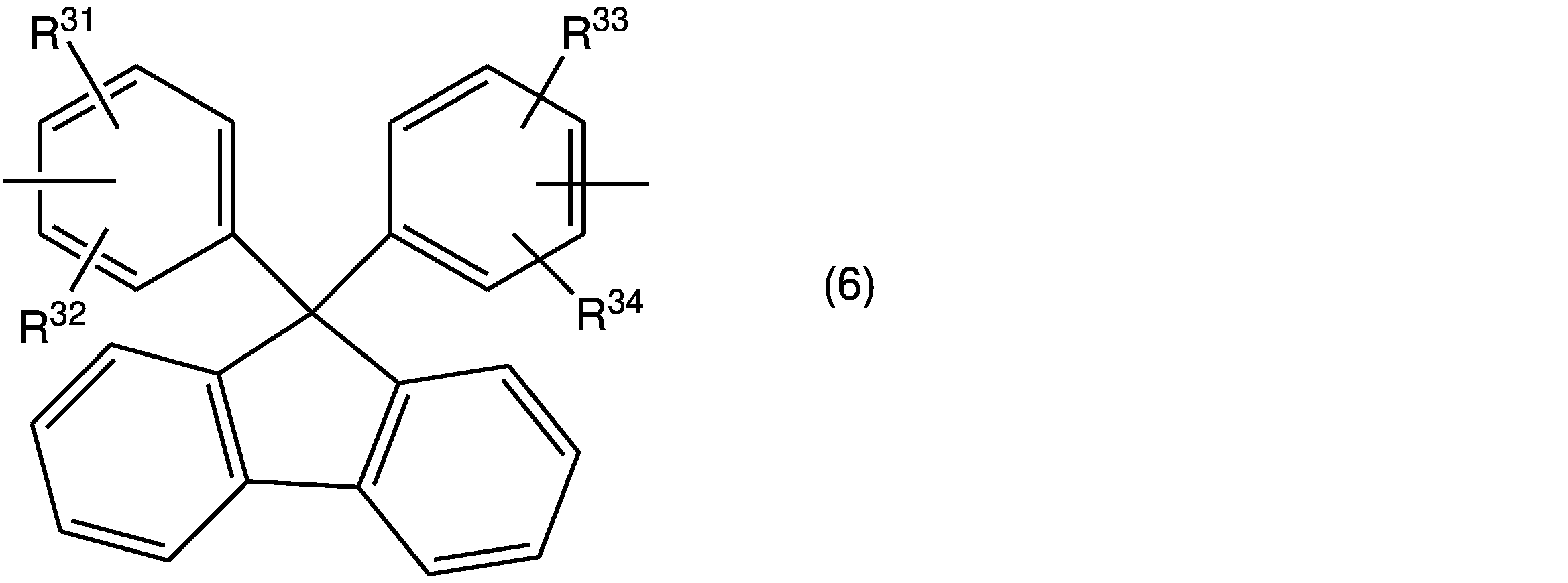
第1の接着剤層1は、導電粒子4(以下、「(A)成分」という場合がある。)、光硬化性樹脂成分(以下、「(B)成分」という場合がある。)の硬化物、及び熱硬化性樹脂成分(以下、「(C)成分」という場合がある。)を含有する。第1の接着剤層1は、例えば、(A)成分、(B)成分、及び(C)成分を含有する組成物からなる組成物層に対して光エネルギーを照射し、(B)成分に含まれる成分を重合させ、(B)成分を硬化させることによって得ることができる。第1の接着剤層1は、(A)成分と、(B)成分の硬化物及び(C)成分を含む接着剤成分5とを含有する。(B)成分の硬化物は、(B)成分を完全に硬化させた硬化物であってもよく、(B)成分の一部を硬化させた硬化物であってもよい。(C)成分は、回路接続時に流動可能な成分であり、例えば、未硬化の硬化性樹脂成分である。
(A)成分は、導電性を有する粒子であれば特に制限されず、Au、Ag、Pd、Ni、Cu、はんだ等の金属で構成された金属粒子、導電性カーボンで構成された導電性カーボン粒子などであってよい。(A)成分は、非導電性のガラス、セラミック、プラスチック(ポリスチレン等)などを含む核と、上記金属又は導電性カーボンを含み、核を被覆する被覆層とを備える被覆導電粒子であってもよい。これらの中でも、(A)成分は、好ましくは熱溶融性の金属で形成された金属粒子、又はプラスチックを含む核と、金属又は導電性カーボンを含み、核を被覆する被覆層とを備える被覆導電粒子である。このような被覆導電粒子は、熱硬化性樹脂成分の硬化物を加熱又は加圧により変形させることが容易であるため、電極同士を電気的に接続する際に、電極と(A)成分との接触面積を増加させ、電極間の導電性をより向上させることができる。
単分散率(%)=(0.16mm2中の単分散状態の導電粒子数/0.16mm2中の導電粒子数)×100
(B)成分は、光照射によって硬化する樹脂成分であれば特に制限されないが、接続抵抗がより優れる観点から、ラジカル硬化性を有する樹脂成分であってよい。(B)成分は、例えば、ラジカル重合性化合物(以下、「(B1)成分」という場合がある。)及び光ラジカル重合開始剤(以下、「(B2)成分」という場合がある。)を含んでいてもよい。(B)成分は、(B1)成分及び(B2)成分からなる成分であり得る。
(B1)成分は、光(例えば、紫外光)の照射によって(B2)成分から発生したラジカルによって重合する化合物である。(B1)成分は、モノマー、又は、1種若しくは2種以上のモノマーが重合してなるポリマー(又はオリゴマー)のいずれであってもよい。(B1)成分は、1種を単独で用いてもよく、複数を組み合わせて用いてもよい。
(B2)成分は、150~750nmの範囲内の波長を含む光、好ましくは254~405nmの範囲内の波長を含む光、さらに好ましくは365nmの波長を含む光(例えば紫外光)の照射によってラジカルを発生する光重合開始剤である。(B2)成分は、1種を単独で用いてもよく、複数を組み合わせて用いてもよい。
(C)成分は、例えば、カチオン重合性化合物(以下、「(C1)成分」という場合がある。)及び熱カチオン重合開始剤(以下、「(C2)成分」という場合がある。)を含んでいてもよい。(C)成分は、(C1)成分及び(C2)成分からなる成分であり得る。なお、第1の熱硬化性樹脂成分及び第2の熱硬化性樹脂成分は、それぞれ第1の接着剤層及び第2の接着剤層に含有される熱硬化性樹脂成分を意味する。第1の熱硬化性樹脂成分及び第2の熱硬化性樹脂成分に含まれる成分(例えば、(C1)成分、(C2)成分等)の種類、組み合わせ、及び含有量は、互いに同一であってもよく、異なっていてもよい。
(C1)成分は、熱によって(C2)成分と反応することによって架橋する化合物である。なお、(C1)成分は、ラジカルによって反応するラジカル重合性基を有しない化合物を意味し、(C1)成分は、(B1)成分に包含されない。(C1)成分は、接続抵抗の低減効果がさらに向上し、接続信頼性により優れる観点から、分子中に開環重合性の環状エーテル基を1個以上有する化合物であってよい。(C1)成分は、1種を単独で用いてもよく、複数を組み合わせて用いてもよい。分子中に開環重合性の環状エーテル基を1個以上有する化合物としては、例えば、オキセタン化合物及び脂環式エポキシ化合物からなる群より選ばれる少なくとも1種であってよい。(C1)成分は、所望の溶融粘度が得られ易い観点から、オキセタン化合物の少なくとも1種及び脂環式エポキシ化合物の少なくとも1種の両方を含むことが好ましい。
(C2)成分は、加熱により酸等を発生して重合を開始する熱重合開始剤である。(C2)成分はカチオンとアニオンとから構成される塩化合物であってよい。(C2)成分は、例えば、BF4 -、BR4 -(Rは、2以上のフッ素原子又は2以上のトリフルオロメチル基で置換されたフェニル基を示す。)、PF6 -、SbF6 -、AsF6 -等のアニオンを有する、スルホニウム塩、ホスホニウム塩、アンモニウム塩、ジアゾニウム塩、ヨードニウム塩、アニリニウム塩等のオニウム塩などが挙げられる。また、(C1)成分がエポキシ樹脂を含む場合、(C2)成分として上述したエポキシ樹脂熱硬化剤を用いてもよい。(C2)成分は、1種を単独で用いてもよく、複数を組み合わせて用いてもよい。
第1の接着剤層1は、(A)成分、(B)成分の硬化物、及び(C)成分以外にその他の成分をさらに含有していてもよい。その他の成分としては、例えば、フィルム形成成分(以下、「(D)成分」という場合がある。)、カップリング剤(以下、「(E)成分」という場合がある。)、充填材(以下、「(F)成分」という場合がある。)等が挙げられる。
第1の接着剤層1は、イオン捕捉剤、軟化剤、促進剤、劣化防止剤、着色剤、難燃化剤、チキソトロピック剤等のその他の添加剤をさらに含有していてもよい。その他の添加剤の含有量は、第1の接着剤層の全質量を基準として、例えば、0.1~10質量%であってよい。なお、組成物又は組成物層中のその他の添加剤の含有量(組成物又は組成物層の全質量基準)は上記範囲と同様であってよい。
第2の接着剤層2は、(C)成分を含有する。第2の接着剤層2における(C)成分(すなわち、第2の熱硬化性樹脂成分)は、上述した一般式(1)で表されるフルオレン骨格含有エポキシ樹脂((C-F)成分)及びエポキシ樹脂熱硬化剤を含有することができる。また、(C)成分は、(C1)成分として、(C-F)成分以外の(C1)成分を含んでいてもよい。更に、(C)成分は、エポキシ樹脂熱硬化剤として上述した(C2)成分を含んでいてもよい。なお、(C1)成分及び(C2)成分は、第1の接着剤層1における(C)成分(すなわち、第1の熱硬化性樹脂成分)で使用される(C1)成分及び(C2)成分と同様のものが用いられる。第2の熱硬化性樹脂成分は、第1の熱硬化性樹脂成分と同一であっても、異なっていてもよい。
(最低溶融粘度の測定方法)
各接着剤フィルムを厚さが500μm以上となるようにラミネータで積層して積層体を得る。得られた積層体から離型処理されたPETを剥離し、10.0mm×10.0mmに切り出して測定試料を得る。得られた測定試料を粘弾性測定装置(商品名:ARES-G2、TAインスツルメンツ社製、昇温速度:10℃/min)を用いて最低溶融粘度を測定する。
一実施形態の回路接続用接着剤フィルムの製造方法は、例えば、(A)成分、(B)成分、及び(C)成分(第1の熱硬化性樹脂成分)、並びに必要に応じてその他の成分を含有する組成物からなる組成物層に対して光を照射し、第1の接着剤層を形成する工程(第1の工程)と、第1の接着剤層上に、(C)成分(第2の熱硬化性樹脂成分)、及び必要に応じてその他の成分を含有する第2の接着剤層を積層する工程(第2の工程)とを備えていてもよい。当該製造方法は、第1の接着剤層の第2の接着剤層とは反対側の層上に、(C)成分(第3の熱硬化性樹脂成分)、及び必要に応じてその他の成分を含有する第3の接着剤層を積層する工程(第3の工程)をさらに備えていてもよい。この場合、第2の工程を先に行ってもよく、第3の工程を先に行ってもよい。第3の工程を先に行う場合、第1の接着剤層の第2の接着剤層が積層される予定の側とは反対側に第3の接着剤層を積層される。
以下、回路接続材料として上述の回路接続用接着剤フィルム10を用いた回路接続構造体及びその製造方法について説明する。
[1] 熱硬化性樹脂成分と、導電粒子と、を含み、前記熱硬化性樹脂成分が、下記一般式(1)で表されるフルオレン骨格含有エポキシ樹脂、及び、エポキシ樹脂熱硬化剤を含有する、回路接続用接着剤フィルム。

[2] 前記フルオレン骨格含有エポキシ樹脂の重量平均分子量が、5000~8000である、[1]に記載の回路接続用接着剤フィルム。
[3] 前記フルオレン骨格含有エポキシ樹脂が、85~105℃に軟化点を有する、[1]又は[2]に記載の回路接続用接着剤フィルム。
[4] 前記導電粒子がフィルムの一方の面側に偏在している、[1]~[3]のいずれかに記載の回路接続用接着剤フィルム。
[5] 導電粒子、光硬化性樹脂成分の硬化物、及び第1の熱硬化性樹脂成分を含有する第1の接着剤層と、第1の接着剤層上に設けられた、第2の熱硬化性樹脂成分を含有する第2の接着剤層と、を備え、前記第2の熱硬化性樹脂成分が、下記一般式(1)で表されるフルオレン骨格含有エポキシ樹脂、及び、エポキシ樹脂熱硬化剤を含有する、回路接続用接着剤フィルム。

[6] 前記フルオレン骨格含有エポキシ樹脂の重量平均分子量が、5000~8000である、[5]に記載の回路接続用接着剤フィルム。
[7] 前記フルオレン骨格含有エポキシ樹脂が、85~105℃に軟化点を有する、[5]又は[6]に記載の回路接続用接着剤フィルム。
[8] 第1の電極を有する第1の回路部材と、第2の電極を有する第2の回路部材との間に、[1]~[7]のいずれかに記載の回路接続用接着剤フィルムを介在させ、前記第1の回路部材及び前記第2の回路部材を熱圧着して、前記第1の電極及び前記第2の電極を互いに電気的に接続する工程を備える、回路接続構造体の製造方法。
[9] 第1の電極を有する第1の回路部材と、第2の電極を有する第2の回路部材と、前記第1の回路部材及び前記第2の回路部材の間に配置され、前記第1の電極及び前記第2の電極を互いに電気的に接続する回路接続部と、を備え、前記回路接続部が、[1]~[7]のいずれかに記載の回路接続用接着剤フィルムの硬化物を含む、回路接続構造体。
ポリスチレン粒子の表面上にNiめっきを施した後、最表面にPdで置換めっきを施して、平均粒径3.2μmの導電粒子を作製した。
第1の接着剤層及び第2の接着剤層の作製においては、下記に示す材料を用いた。
A-1:上記で作製した導電粒子
(B1)成分:ラジカル重合性化合物
B1-1:A-BPEF-70T(エトキシ化フルオレン型ジ(メタ)アクリレート(2官能)、新中村化学工業株式会社製、商品名)、トルエンで不揮発分70質量%に希釈したものを使用
B1-2:リポキシ VR-90(ビスフェノールA型エポキシ(メタ)アクリレート(2官能)(ビニルエステル樹脂)、昭和電工株式会社製、商品名)
B2-1:Irgacure OXE-02(エタノン,1-[9-エチル-6-(2-メチルベンゾイル)-9H-カルバゾール-3-イル]-,1-(0-アセチルオキシム)、BASF社製、商品名)、MEKで不揮発分10質量%に希釈したものを使用
(C1)成分:カチオン重合性化合物
C1-1:ETERNACOLL OXBP(3-エチル-3-ヒドロキシメチルオキセタン、宇部興産株式会社製、商品名)
C1-2:EHPE3150(2,2-ビス(ヒドロキシメチル)-1-ブタノールの1,2-エポキシ-4-(2-オキシラニル)シクロヘキサン付加物、株式会社ダイセル株式会社製、商品名)
C1-3:OX-SQ TX-100(ポリ({3-[(3-エチル-3-オキセタニル)メトキシ]プロピル}シルセスキオキサン)誘導体、東亜合成株式会社製、商品名)
C1-4:セロキサイド2021P(3’,4’-エポキシシクロヘキシルメチル 3,4-エポキシシクロヘキサンカルボキシレート、株式会社ダイセル株式会社製、商品名)
C1-5:YL980(ビスフェノールA型エポキシ樹脂、エポキシ当量:180~190、重量平均分子量:362、三菱ケミカル株式会社製、商品名)
C1-6:jER1007(エポキシ樹脂、エポキシ当量:180~190、重量平均分子量:10,000、三菱化学株式会社製、商品名)、有機溶媒で不揮発分70質量%に希釈したものを使用
C1-7:jER1010(ビスフェノールA型固形エポキシ樹脂、エポキシ当量:3000~5000、重量平均分子量:40000、三菱化学株式会社製、商品名)
C-F-1:TOPR-300(高Tgタイプエポキシ樹脂、エポキシ当量:900~1,000、重量平均分子量:6700、軟化点:91℃、日鉄ケミカル&マテリアル株式会社製、商品名)、MEKで不揮発分60質量%に希釈したものを使用
C2-1:CXC-1821(King Industries社製、商品名)
D-1:FX293(フルオレン骨格含有型フェノキシ樹脂、重量平均分子量:32,000、ガラス転移温度:152℃、日鉄ケミカル&マテリアル株式会社製、商品名)、MEKで不揮発分35質量%に希釈したものを使用
E-1:KBM-303(エチルトリメトキシシラン、信越化学工業株式会社製、商品名)
F-1:アドマファイン SE2050(シリカ微粒子、株式会社アドマテックス製、商品名)
検出器:日立ハイテクサイエンス製L-2490-RI
カラム:Gelpack GL-R440+R450+R400M
流量:2.05ml/min
濃度:5mg/ml
注入量:200μl
カラム温度:40℃
溶離液:THF
標準サンプル:ポリスチレン
熱機械分析装置:日立ハイテクサイセンス製TMA-7100型、Penetration(針入、Φ1mm)モード
昇温速度:10℃/min
荷重:98.1mN
表1に示す材料を表1に示す組成比(表1の数値は不揮発分量を意味する。)で混合した組成物を得た後、離型処理されたPET(ポリエチレンテレフタレート)フィルムの上に磁場を掛けながら塗工し、有機溶媒等を70℃で5分間熱風乾燥することによって、各成分を含有する組成物からなる組成物層をそれぞれ得た。組成物層は、乾燥後の厚さがそれぞれ3~4μmとなるように塗工した。その後、組成物層に対してそれぞれ光照射することによって(UV照射:メタルハライドランプ、積算光量:1000~3000mJ/cm2)、導電粒子が分散した第1の接着剤層を作製した。ここでの厚さは接触式厚み計を用いて測定した。
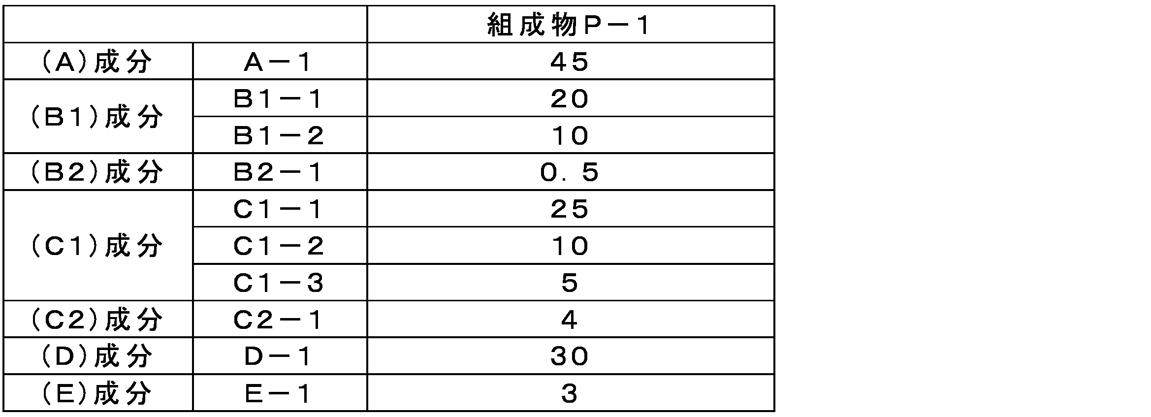
表2に示す材料を表2に示す組成比(表2の数値は不揮発分量を意味する。)で混合した組成物を得た後、離型処理されたPET(ポリエチレンテレフタレート)フィルムの上に塗工し、有機溶媒等を70℃で5分間熱風乾燥することによって、各成分を含有する組成物からなる第2の組成物層をそれぞれ作製した。組成物層は、乾燥後の厚さがそれぞれ8~9μmとなるように塗工した。ここでの厚さは接触式厚み計を用いて測定した。こうして、PETフィルム上に第2の接着剤層を作製した。

[接着剤フィルムの作製]
上記で作製した第1の接着剤層及び第2の接着剤層を用いて、表3に示す構成の接着剤フィルムを作製した。例えば、実施例1の接着剤フィルムにおいては、組成物S-1によって形成した第2の接着剤層に、組成物P-1によって形成した第1の接着剤層を50~60℃の温度をかけながら張り合わせて、実施例1の接着剤フィルムを得た。実施例2~3及び比較例1~5の接着剤フィルムについては、実施例1と同様にして、表3に示す構成の接着剤フィルムを作製した。
<回路接続構造体の作製>
第1の回路部材として、バンプ電極を2列で千鳥状に配列したICチップ(0.9mm×20.3mm、厚さ:0.3mm、バンプ電極の大きさ:70μm×12μm、バンプ電極間スペース:12μm、バンプ電極厚さ:9μm)を準備した。また、第2の回路部材として、ポリイミド基板(東レ・デュポン株式会社製、200H)(38mm×28mm、厚さ:0.05mm)の表面に、Ti:50nm/Al:400nmの配線パターン(パターン幅:17μm、電極間スペース:7μm)を形成したものを準備した。
作製した回路接続構造体について、初期の接続抵抗(導通抵抗)を4端子法によって測定した。測定には、マルチメータ(7461A、株式会社エーディーシー製)を用いた。電位差を任意の14点で測定し、その平均値を求めた。電位差の平均値を接続抵抗値に換算し、下記の基準で評価した。結果を表3に示す。
A:接続抵抗値が1.0Ω未満
B:接続抵抗値が1.0Ω以上3.0Ω未満
C:接続抵抗値が3.0Ω以上
A:接続抵抗値が1.0Ω未満
B:接続抵抗値が1.0Ω以上3.0Ω未満
C:接続抵抗値が3.0Ω以上
(接着剤フィルム(テープ)のリール体の作製)
上記で得られた接着剤フィルム(第1の接着剤層/第2の接着剤層/PETフィルム)を、ロールツーロールのスリット設備により幅0.6mmに裁断し、リール部品(巻芯外径:66mm、プラスチック成型品)に、100mの長さで接着剤テープを巻き取った。このとき、第1の接着剤層が巻芯側(内側)を向き、PETフィルムが外側を向くように巻き取った。巻芯の両側にはリール側板(厚さ2.0mm)が設けられており、このリール側板と接着剤テープの巻重体との間の隙間距離は、左右それぞれ約0.1mm~0.5mmの範囲内であった。
リール体を縦にした状態で固定し、先端に75gの分銅を吊り下げ、温度30℃の恒温槽(相対湿度40~60%)内に6時間にわたって放置した。その後、テンシロン(商品名、株式会社エー・アンド・デイ製)を使用し、リール体から接着剤テープを1m/分の速度で引き出し、顕微鏡にて観察し、下記の基準で耐背面転写性を評価した。
OK:100mの長さにわたって、5mm以上の接着剤フィルムの背面転写(第2の接着剤層とPETフィルムと間に剥がれ)が見られなかった
NG:100mの長さのうちに、5mm以上の接着剤フィルムの背面転写が見られた
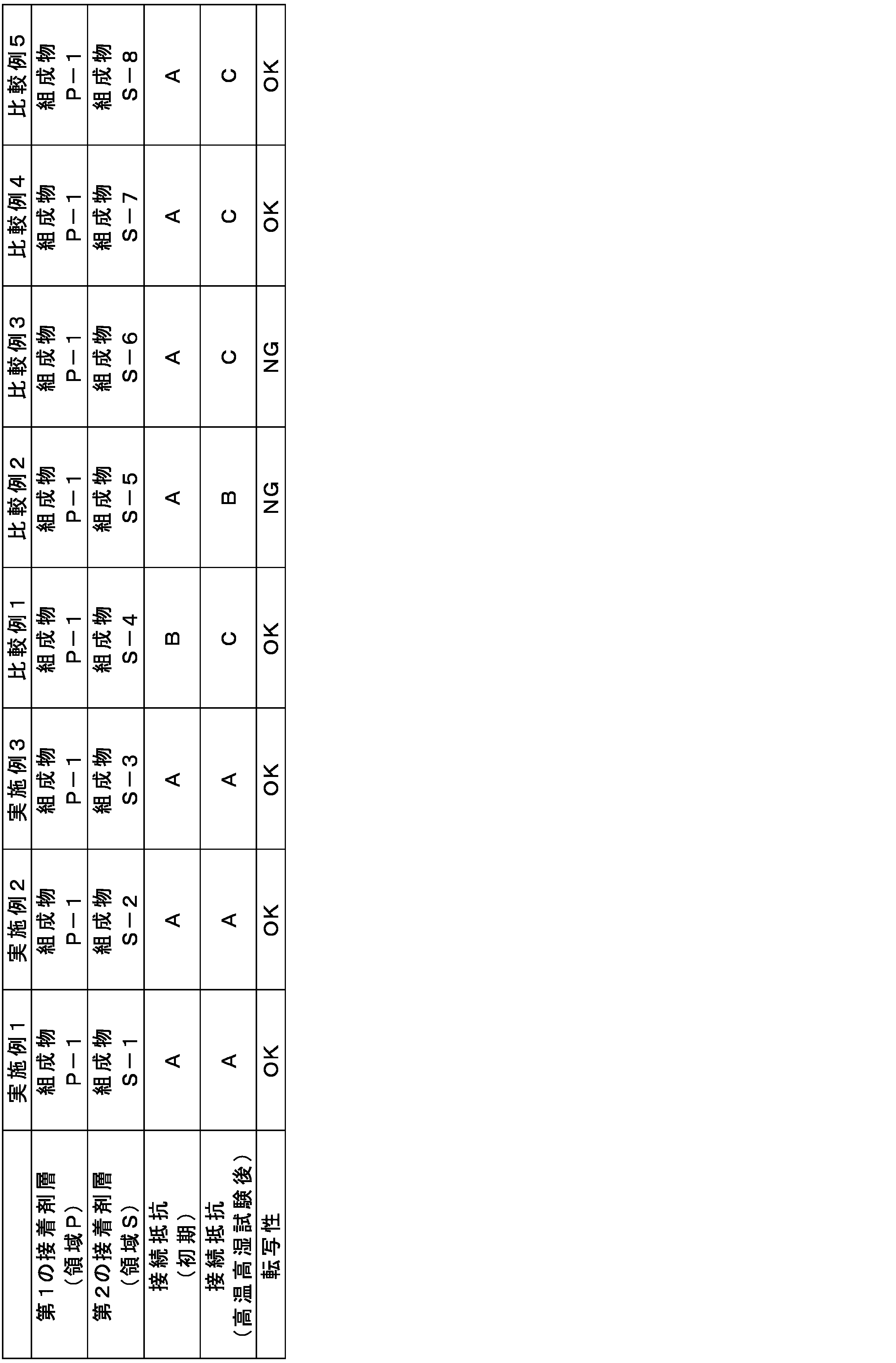
Claims (9)
- 熱硬化性樹脂成分と、導電粒子と、を含み、
前記熱硬化性樹脂成分が、下記一般式(1)で表されるフルオレン骨格含有エポキシ樹脂、及び、エポキシ樹脂熱硬化剤を含有する、回路接続用接着剤フィルム。

- 前記フルオレン骨格含有エポキシ樹脂の重量平均分子量が、5000~8000である、請求項1に記載の回路接続用接着剤フィルム。
- 前記フルオレン骨格含有エポキシ樹脂が、85~105℃に軟化点を有する、請求項1に記載の回路接続用接着剤フィルム。
- 前記導電粒子がフィルムの一方の面側に偏在している、請求項1に記載の回路接続用接着剤フィルム。
- 導電粒子、光硬化性樹脂成分の硬化物、及び第1の熱硬化性樹脂成分を含有する第1の接着剤層と、第1の接着剤層上に設けられた、第2の熱硬化性樹脂成分を含有する第2の接着剤層と、を備え、
前記第2の熱硬化性樹脂成分が、下記一般式(1)で表されるフルオレン骨格含有エポキシ樹脂、及び、エポキシ樹脂熱硬化剤を含有する、回路接続用接着剤フィルム。

- 前記フルオレン骨格含有エポキシ樹脂の重量平均分子量が、5000~8000である、請求項5に記載の回路接続用接着剤フィルム。
- 前記フルオレン骨格含有エポキシ樹脂が、85~105℃に軟化点を有する、請求項5に記載の回路接続用接着剤フィルム。
- 第1の電極を有する第1の回路部材と、第2の電極を有する第2の回路部材との間に、請求項1~7のいずれか一項に記載の回路接続用接着剤フィルムを介在させ、前記第1の回路部材及び前記第2の回路部材を熱圧着して、前記第1の電極及び前記第2の電極を互いに電気的に接続する工程を備える、回路接続構造体の製造方法。
- 第1の電極を有する第1の回路部材と、
第2の電極を有する第2の回路部材と、
前記第1の回路部材及び前記第2の回路部材の間に配置され、前記第1の電極及び前記第2の電極を互いに電気的に接続する回路接続部と、
を備え、
前記回路接続部が、請求項1~7のいずれか一項に記載の回路接続用接着剤フィルムの硬化物を含む、回路接続構造体。
Priority Applications (3)
| Application Number | Priority Date | Filing Date | Title |
|---|---|---|---|
| KR1020257031975A KR20250163900A (ko) | 2023-04-13 | 2024-04-09 | 회로 접속용 접착제 필름, 및 회로 접속 구조체 및 그 제조 방법 |
| CN202480021159.3A CN121153339A (zh) | 2023-04-13 | 2024-04-09 | 电路连接用黏合剂膜、以及电路连接结构体及其制造方法 |
| JP2025513961A JPWO2024214701A1 (ja) | 2023-04-13 | 2024-04-09 |
Applications Claiming Priority (2)
| Application Number | Priority Date | Filing Date | Title |
|---|---|---|---|
| JP2023-065696 | 2023-04-13 | ||
| JP2023065696 | 2023-04-13 |
Publications (1)
| Publication Number | Publication Date |
|---|---|
| WO2024214701A1 true WO2024214701A1 (ja) | 2024-10-17 |
Family
ID=93059434
Family Applications (1)
| Application Number | Title | Priority Date | Filing Date |
|---|---|---|---|
| PCT/JP2024/014419 Ceased WO2024214701A1 (ja) | 2023-04-13 | 2024-04-09 | 回路接続用接着剤フィルム、並びに回路接続構造体及びその製造方法 |
Country Status (5)
| Country | Link |
|---|---|
| JP (1) | JPWO2024214701A1 (ja) |
| KR (1) | KR20250163900A (ja) |
| CN (1) | CN121153339A (ja) |
| TW (1) | TW202442840A (ja) |
| WO (1) | WO2024214701A1 (ja) |
Citations (4)
| Publication number | Priority date | Publication date | Assignee | Title |
|---|---|---|---|---|
| WO2008015852A1 (fr) * | 2006-08-04 | 2008-02-07 | Hitachi Chemical Company, Ltd. | Composition adhésive et structure de connexion pour élément de circuit |
| WO2008152711A1 (ja) * | 2007-06-13 | 2008-12-18 | Hitachi Chemical Company, Ltd. | 回路接続用フィルム状接着剤 |
| JP2011165758A (ja) * | 2010-02-05 | 2011-08-25 | Hitachi Chem Co Ltd | 回路部材接続用接着剤及びこれを用いた半導体装置 |
| WO2021251386A1 (ja) * | 2020-06-11 | 2021-12-16 | 昭和電工マテリアルズ株式会社 | 回路接続用接着剤フィルム、並びに回路接続構造体及びその製造方法 |
Family Cites Families (1)
| Publication number | Priority date | Publication date | Assignee | Title |
|---|---|---|---|---|
| JP2016054288A (ja) | 2014-09-02 | 2016-04-14 | デクセリアルズ株式会社 | 接続体、接続体の製造方法、電子部品の接続方法、及び電子部品 |
-
2024
- 2024-04-09 CN CN202480021159.3A patent/CN121153339A/zh active Pending
- 2024-04-09 WO PCT/JP2024/014419 patent/WO2024214701A1/ja not_active Ceased
- 2024-04-09 JP JP2025513961A patent/JPWO2024214701A1/ja active Pending
- 2024-04-09 KR KR1020257031975A patent/KR20250163900A/ko active Pending
- 2024-04-11 TW TW113113490A patent/TW202442840A/zh unknown
Patent Citations (4)
| Publication number | Priority date | Publication date | Assignee | Title |
|---|---|---|---|---|
| WO2008015852A1 (fr) * | 2006-08-04 | 2008-02-07 | Hitachi Chemical Company, Ltd. | Composition adhésive et structure de connexion pour élément de circuit |
| WO2008152711A1 (ja) * | 2007-06-13 | 2008-12-18 | Hitachi Chemical Company, Ltd. | 回路接続用フィルム状接着剤 |
| JP2011165758A (ja) * | 2010-02-05 | 2011-08-25 | Hitachi Chem Co Ltd | 回路部材接続用接着剤及びこれを用いた半導体装置 |
| WO2021251386A1 (ja) * | 2020-06-11 | 2021-12-16 | 昭和電工マテリアルズ株式会社 | 回路接続用接着剤フィルム、並びに回路接続構造体及びその製造方法 |
Also Published As
| Publication number | Publication date |
|---|---|
| CN121153339A (zh) | 2025-12-16 |
| KR20250163900A (ko) | 2025-11-21 |
| JPWO2024214701A1 (ja) | 2024-10-17 |
| TW202442840A (zh) | 2024-11-01 |
Similar Documents
| Publication | Publication Date | Title |
|---|---|---|
| CN101120440A (zh) | 区域安装型半导体装置及用于该半导体装置的小片接合用树脂组合物、密封用树脂组合物 | |
| KR102942678B1 (ko) | 회로 접속용 접착제 필름, 및 회로 접속 구조체 및 그 제조 방법 | |
| US20230234333A1 (en) | Adhesive film for circuit connection, and circuit connection structure and manufacturing method therefor | |
| KR20240118834A (ko) | 회로 접속용 접착제 필름, 및 회로 접속 구조체 및 그 제조 방법 | |
| KR20250054076A (ko) | 회로 접속용 접착제 필름 및 접속 구조체, 및, 이들의 제조 방법 | |
| TW202224942A (zh) | 電路連接用接著劑薄膜及其製造方法、以及電路連接結構體及其製造方法 | |
| JP7800429B2 (ja) | 回路接続用接着剤フィルム、回路接続用接着剤組成物、並びに回路接続構造体及びその製造方法 | |
| JP2023063770A (ja) | 回路接続用接着剤フィルム、並びに回路接続構造体及びその製造方法 | |
| KR20250044733A (ko) | 회로 접속용 접착제 필름, 및 회로 접속 구조체 및 그 제조 방법 | |
| KR20250163900A (ko) | 회로 접속용 접착제 필름, 및 회로 접속 구조체 및 그 제조 방법 | |
| KR20240118833A (ko) | 회로 접속용 접착제 필름, 및 회로 접속 구조체 및 그 제조 방법 | |
| JP2022158554A (ja) | 回路接続用接着剤フィルム、並びに回路接続構造体及びその製造方法 | |
| WO2022075370A1 (ja) | 回路接続用接着剤フィルム、回路接続用材料、並びに回路接続構造体及びその製造方法 | |
| JP2022061623A (ja) | 回路接続用接着剤フィルム、並びに回路接続構造体及びその製造方法 | |
| JP7859314B2 (ja) | 回路接続用接着剤フィルム、並びに回路接続構造体及びその製造方法 | |
| JP7622448B2 (ja) | 回路接続用接着剤及び接続構造体の製造方法 | |
| TW202212519A (zh) | 電路連接用接著劑膜、含無機填料組成物、以及電路連接結構體及其製造方法 | |
| JP2025034613A (ja) | 回路接続用接着剤フィルム、並びに回路接続構造体及びその製造方法 | |
| JP2025034640A (ja) | 回路接続用接着剤フィルム、並びに回路接続構造体及びその製造方法 | |
| WO2025100136A1 (ja) | 回路接続構造体の製造方法、回路接続用接着剤フィルム、及び回路接続構造体 | |
| WO2025100135A1 (ja) | 回路接続構造体の製造方法、回路接続用接着剤フィルム、及び回路接続構造体 |
Legal Events
| Date | Code | Title | Description |
|---|---|---|---|
| 121 | Ep: the epo has been informed by wipo that ep was designated in this application |
Ref document number: 24788725 Country of ref document: EP Kind code of ref document: A1 |
|
| ENP | Entry into the national phase |
Ref document number: 2025513961 Country of ref document: JP Kind code of ref document: A |
|
| WWE | Wipo information: entry into national phase |
Ref document number: 2025513961 Country of ref document: JP |
|
| ENP | Entry into the national phase |
Ref document number: 1020257031975 Country of ref document: KR Free format text: ST27 STATUS EVENT CODE: A-0-1-A10-A15-NAP-PA0105 (AS PROVIDED BY THE NATIONAL OFFICE) |
|
| WWE | Wipo information: entry into national phase |
Ref document number: KR1020257031975 Country of ref document: KR |
|
| NENP | Non-entry into the national phase |
Ref country code: DE |
|
| 122 | Ep: pct application non-entry in european phase |
Ref document number: 24788725 Country of ref document: EP Kind code of ref document: A1 |