WO2024204344A1 - 積層体の製造方法 - Google Patents
積層体の製造方法 Download PDFInfo
- Publication number
- WO2024204344A1 WO2024204344A1 PCT/JP2024/012248 JP2024012248W WO2024204344A1 WO 2024204344 A1 WO2024204344 A1 WO 2024204344A1 JP 2024012248 W JP2024012248 W JP 2024012248W WO 2024204344 A1 WO2024204344 A1 WO 2024204344A1
- Authority
- WO
- WIPO (PCT)
- Prior art keywords
- substrate
- manufacturing
- less
- laminate according
- resin
- Prior art date
- Legal status (The legal status is an assumption and is not a legal conclusion. Google has not performed a legal analysis and makes no representation as to the accuracy of the status listed.)
- Ceased
Links
Images

Classifications
-
- G—PHYSICS
- G02—OPTICS
- G02B—OPTICAL ELEMENTS, SYSTEMS OR APPARATUS
- G02B6/00—Light guides; Structural details of arrangements comprising light guides and other optical elements, e.g. couplings
- G02B6/10—Light guides; Structural details of arrangements comprising light guides and other optical elements, e.g. couplings of the optical waveguide type
- G02B6/12—Light guides; Structural details of arrangements comprising light guides and other optical elements, e.g. couplings of the optical waveguide type of the integrated circuit kind
- G02B6/13—Integrated optical circuits characterised by the manufacturing method
Definitions
- the present invention relates to a method for manufacturing a laminate.
- optical/electrical composite substrate is one in which an optical waveguide is provided on a substrate.
- Techniques relating to a method for manufacturing an optical waveguide include those described in, for example, Patent Documents 1 to 3.
- Patent Document 1 describes a method for producing an embedded polyimide optical waveguide, which is characterized in that an upper cladding is placed between an arbitrary substrate and a ridge-type waveguide, and the upper cladding has the same heat resistance as the substrate and an adhesive with a lower refractive index than the core. According to the method for producing a polyimide optical waveguide described in Patent Document 1, it is described that a polyimide optical waveguide can be produced on any substrate.
- Patent Document 2 describes an opto-electrical hybrid board comprising a flexible circuit board in which electrical wiring having mounting pads is formed on the surface of an insulating layer, an element mounted on the mounting pad, and an optical waveguide laminated on the back surface side of the insulating layer, wherein the flexible circuit board is a flexible double-sided circuit board in which electrical wiring is also formed on the back surface of the insulating layer, and a metallic reinforcing layer is plated on at least the portion of the electrical wiring on the back surface side that corresponds to the mounting pad, and the optical waveguide is in contact with the metallic reinforcing layer.
- an optical-electrical hybrid board According to the optical-electrical hybrid board described in Patent Document 2, a metallic reinforcing layer is adhered to an insulating layer of a flexible circuit board without an adhesive layer, and it is described that an optical-electrical hybrid board can be provided in which elements are properly mounted while suppressing deformation due to a pressure load when the elements are mounted by the metallic reinforcing layer.
- Patent Document 2 describes a method of preparing a substrate having copper foil 21 formed on both sides of an insulating layer 1 made of a resin such as polyimide, and forming through holes 1a and via holes 1b for an optical path in the substrate (see paragraph 0023 of Patent Document 2).
- Patent Document 2 also describes a flexible double-sided circuit board E on which a metallic reinforcing layer M is formed (see paragraph 0028 of Patent Document 2).
- the flexible double-sided circuit board E includes the substrate.
- Patent Document 2 describes that an undercladding layer 6 is formed on the back side of a flexible double-sided circuit board E in contact with a metal reinforcing layer M that covers the electrical wiring 2B on the back side, and describes that examples of the molding material for the undercladding layer 6 include photosensitive resins and thermosetting resins (see paragraph 0029 of Patent Document 2). According to Figures 4 to 6 of Patent Document 2, it can be seen that the molding material for the undercladding layer 6 is filled into the recesses formed in the flexible double-sided circuit board E on which the metal reinforcing layer M is formed.
- Patent Document 3 describes an optoelectronic wiring board that is formed by integrating a rigid section in which conductor circuits and insulating layers are laminated on both sides of a substrate with one or more bendable flex sections, wherein the rigid section is formed with external connection terminals for mounting optical elements and/or package substrates on which optical elements are mounted, and at least one of the flex sections is formed with optical wiring. According to the optoelectronic wiring board of Patent Document 3, it is described that large-volume information processing and high-speed information processing can be suitably performed without increasing the size of the wiring board.
- Patent Document 3 describes that the rigid section has an optical signal passing region formed therein, and that the optical signal passing region is filled with a resin composition (see claims 4 and 5 of Patent Document 3). Furthermore, it describes that the optical signal passing region is formed so as to penetrate all of the substrates and insulating layers that make up the rigid section (see claim 6 of Patent Document 3).
- Patent Document 3 describes a substrate 221 consisting of an optical waveguide film 250 and a surrounding resin layer (insulating layer) 221a, and describes that the resin layer 221a constitutes part of the optical signal transmitting regions 242a, 242b (see paragraph 0033 of Patent Document 3).
- the manufacturing process for optoelectronic composite substrates includes, for example, a process of integrating a substrate having a through-hole with a film for optical waveguide clad.
- the through-hole formed in the substrate needs to be filled with optical waveguide clad (hereinafter, “embeddability” refers to the property of the degree to which the optical waveguide clad can be embedded in the through-hole).
- the present invention has been made in consideration of the above circumstances, and provides a method for manufacturing a laminate that can produce an optoelectronic composite substrate with improved embeddability.
- the present invention provides the following method for producing a laminate.
- a method for manufacturing a laminate including a substrate having a through hole and a first clad layer of an optical waveguide comprising the steps of: A step (A) of preparing a workpiece on which a resin film having a resin layer (a) made of a resin composition for forming the first clad layer is placed on the substrate; and (B) laminating the first clad layer onto the substrate by heating and pressing the work under reduced pressure using a vacuum laminating device.
- T/R is 0.10 or more, where T [ ⁇ m] is a thickness of the substrate and R [ ⁇ m] is a hole diameter of the through hole.
- [3] The method for producing a laminate according to [1] or [2] above, wherein the through holes have a hole diameter of 10 ⁇ m or more and 1000 ⁇ m or less.
- [4] The method for producing a laminate according to any one of the above [1] to [3], wherein the thickness of the substrate is 10 ⁇ m or more and 1000 ⁇ m or less.
- [5] The method for producing a laminate according to any one of the above [1] to [4], wherein the resin layer (a) has a thickness of 10 ⁇ m or more and 300 ⁇ m or less.
- [6] The method for producing a laminate according to any one of the above [1] to [5], wherein a thickness of the resin layer (a) is smaller than a thickness of the substrate.
- [14] The method for producing a laminate according to any one of [1] to [13], further comprising, after the step (B), a step (C) of sandwiching the workpiece between two press plates and heating and pressing the workpiece.
- [15] The method for producing a laminate according to any one of [1] to [14], wherein, when the volume of the through hole in the laminate is taken as 100 volume %, 70 volume % or more of the through hole is filled with the resin composition for forming the first clad layer.
- [16] The method for producing a laminate according to any one of [1] to [15], wherein the laminate is an optical/electrical composite substrate further comprising a core layer and a second clad layer in this order on the first clad layer.
- the present invention provides a method for manufacturing a laminate that can produce an optoelectronic composite substrate with improved embeddability.
- FIG. 1 is a cross-sectional view showing a schematic example of a structure of an optical/electrical composite substrate according to an embodiment of the present invention.
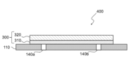
- 4 is a cross-sectional view showing a schematic example of a structure of a workpiece in step (A).
- FIG. 1 is a cross-sectional view showing a schematic example of a structure of an optical/electrical composite substrate according to an embodiment of the present invention.
- 4 is a cross-sectional view showing a schematic example of a structure of a workpiece in step (A).
- the optical/electrical composite substrate 200 has an optical waveguide 100 provided on a substrate 110.
- the optical waveguide 100 has a first clad layer 20, a core layer 30, and a second clad layer 40 laminated in this order.
- a mirror 50 on the light-emitting element side and a mirror 60 on the light-receiving element side are formed in the optical waveguide 100.
- the substrate 110 has through holes 140 (140a, 140b) (note that the through holes 140 shown in Fig. 1 are filled with the first clad layer 20).
- a light-emitting element 120 and a light-receiving element 130 are provided on the side of the substrate 110 opposite to the optical waveguide 100 side.
- the light propagation path in the photoelectric composite substrate 200 will be specifically described using Figure 1.
- the light emitted from the light-emitting portion of the light-emitting element 120 passes through the through-hole 140a formed in the substrate 110, enters the mirror 50 on the light-emitting element side, and is transmitted through the core layer 30. After that, it enters the mirror 60 on the light-receiving element side, passes through the through-hole 140b formed in the substrate 110, and enters the light-receiving element 130.
- the arrows in Figure 1 are a schematic representation of the propagation of light.
- the first clad layer cannot be sufficiently embedded in the through-hole formed in the substrate, and thus a depression may occur on the surface of the optical waveguide clad opposite to the substrate side (i.e., the core layer side of the first clad layer) or a void may occur in the through-hole.
- the through-hole is a propagation path of light, and it was found that when the above-mentioned depression or void occurs in the optical/electrical composite substrate, an optical loss occurs at the interface of the depression or void.
- the present invention has been made in consideration of the above circumstances, and provides a method for producing a laminate that can provide an optoelectronic composite substrate with improved embeddability.
- the method for manufacturing a laminate is a method for manufacturing a laminate comprising a substrate having a through hole and a first clad layer of an optical waveguide, and includes at least a step (A) of preparing a workpiece on which a resin film having a resin layer (a) made of a resin composition for forming the first clad layer is placed on the substrate, and a step (B) of laminating the first clad layer onto the substrate by heating and pressing the workpiece under reduced pressure using a vacuum laminating device.
- the method for manufacturing a laminate of this embodiment includes a step (A) of preparing a workpiece on which a resin film having a resin layer (a) made of a resin composition for forming a first clad layer is placed on a substrate.
- the workpiece 400 has a resin film 300 placed on a substrate 110, the resin film 300 including a resin layer (a) 310 made of a resin composition for forming a first clad layer.
- a through hole 140 is formed in the substrate 110.
- the resin film 300 may be a single-layer film composed only of the resin layer (a) 310, or may be a multi-layer film as shown in FIG. 2, but is preferably a film in which the resin layer (a) 310 and a base film 320 are laminated.
- the resin film 300 includes the base film 320, the handleability of the resin film 300 is improved, and contamination of the vacuum laminating device can be prevented.
- the resin film 300 is a multi-layer film, the workpiece 400 is placed on the substrate 110 with the resin film 300 placed on the substrate 110 such that the resin layer (a) 310 faces the substrate 110 .
- the substrate 110 is not particularly limited as long as it is a substrate having a through hole.
- Examples of the substrate 110 include a printed circuit board and a flexible substrate, and the like.
- a flexible substrate is preferable, and a flexible double-sided copper-clad laminate is more preferable.
- the thickness of the substrate 110 is preferably 10 ⁇ m or more, more preferably 30 ⁇ m or more, even more preferably 40 ⁇ m or more, and even more preferably 45 ⁇ m or more, and from the viewpoint of miniaturizing the optoelectronic composite substrate, it is preferably 1000 ⁇ m or less, more preferably 800 ⁇ m or less, even more preferably 500 ⁇ m or less, even more preferably 300 ⁇ m or less, even more preferably 200 ⁇ m or less, even more preferably 100 ⁇ m or less, and even more preferably 80 ⁇ m or less.
- the substrate 110 has at least one through-hole 140 , and may have one through-hole 140 or may have two or more through-holes 140 .
- the through hole 140 serves as a light propagation path, so the substrate 110 has a through hole 140a on the light emitting element side and a through hole 140b on the light receiving element side.
- the hole diameter of the through hole 140 is preferably 10 ⁇ m or more, more preferably 30 ⁇ m or more, even more preferably 50 ⁇ m or more, even more preferably 70 ⁇ m or more, even more preferably 90 ⁇ m or more, and preferably 1000 ⁇ m or less, more preferably 800 ⁇ m or less, even more preferably 500 ⁇ m or less, even more preferably 400 ⁇ m or less, even more preferably 350 ⁇ m or less, even more preferably 140 ⁇ m or less.
- the substrate 110 has a plurality of through holes 140, it is sufficient that the hole diameter of at least one of the through holes 140 is within the above range.
- T/R is preferably 0.10 or more, more preferably 0.13 or more, even more preferably 0.15 or more, even more preferably 0.20 or more, even more preferably 0.25 or more, even more preferably 0.27 or more, even more preferably 0.30 or more, even more preferably 0.35 or more, even more preferably 0.40 or more, even more preferably 0.45 or more, and even more preferably 0.60 or more, and the upper limit is not particularly limited, but may be, for example, 2.00 or less, 1.50 or less, or 1.00 or less.
- the substrate 110 has a plurality of through holes 140
- the T/R of at least one of the through holes 140 falls within the above range.
- the larger the T/R the more difficult it is to sufficiently fill the through hole with the first clad layer.
- the method for manufacturing a laminate of the present embodiment even when the T/R is large, it is possible to sufficiently fill the through hole with the first clad layer.
- the method for producing a laminate of this embodiment includes a step (B) of laminating a first cladding layer onto a substrate by heating and pressing a workpiece under reduced pressure using a vacuum laminator.
- the substrate and the resin layer (a) can be laminated by heating and pressing the workpiece under reduced pressure. Since the resin layer (a) is made of the resin composition for forming the first clad layer, in other words, the substrate and the first clad layer can be laminated by heating and pressing the workpiece under reduced pressure.
- step (B) the workpiece is heated and pressed under reduced pressure.
- reduced pressure means that the degree of vacuum is smaller than normal pressure (1013 hPa).
- the degree of vacuum is preferably 500 Pa or less, more preferably 400 Pa or less, even more preferably 350 Pa or less, and even more preferably 320 Pa or less.
- the lower limit is not particularly limited, but may be, for example, 10 Pa or more, or 50 Pa or more.
- the pressure when pressing the workpiece is preferably 0.3 MPa or more, more preferably 0.5 MPa or more, even more preferably 1.0 MPa or more, even more preferably 1.3 MPa or more, even more preferably 2.0 MPa or more, even more preferably 3.0 MPa or more, even more preferably 4.0 MPa or more, from the viewpoint of further improving embeddability, and is preferably 10.0 MPa or less, more preferably 8.0 MPa or less, even more preferably 6.0 MPa or less, from the viewpoint of preventing damage to the substrate.
- the temperature of the workpiece when it is heated and pressed is, from the viewpoint of further improving embeddability, preferably 80°C or higher, more preferably 90°C or higher, even more preferably 95°C or higher, and preferably 190°C or lower, more preferably 180°C or lower, even more preferably 150°C or lower, even more preferably 145°C or lower.
- the temperature of the workpiece may be considered to be the same as the set press temperature of the vacuum laminator, because the workpiece is thin and therefore the temperature of the workpiece is considered to reach the same temperature as the set press temperature within a few seconds after being placed in the vacuum laminator.
- the time for pressing the workpiece is preferably 30 seconds or more, more preferably 60 seconds or more, even more preferably 80 seconds or more, and even more preferably 100 seconds or more, from the viewpoint of further improving embeddability, and is preferably 210 seconds or less, more preferably 180 seconds or less, even more preferably 150 seconds or less, and even more preferably 130 seconds or less, from the viewpoint of further improving productivity.
- step (B) the method for heating and pressing the workpiece is not particularly limited, and may be a plate press or a roll press.
- the method of heating and pressing the workpiece is preferably a plate pressing method.
- the workpiece is preferably sandwiched between two press plates and heated and pressed.
- step (B) when the workpiece is sandwiched between two press plates and heated and pressed, it is preferable that at least one of the two press plates contains rubber, and it is preferable that both of the two press plates contain rubber.
- the rubber is not particularly limited, but examples thereof include silicone rubber, fluororubber, and acrylic rubber.
- the press plate has a structure of two or more layers, it is preferable that the surface of the press plate that comes into contact with the workpiece contains rubber.
- the vacuum laminating device is not particularly limited, but for example, a rubber press type laminator, a diaphragm type laminator, etc. can be used, and preferably a rubber press type laminator is used.
- rubber press laminators include CVP-600 (manufactured by Nikko Materials Co., Ltd.) and CVP-700 (manufactured by Nikko Materials Co., Ltd.).
- diaphragm laminators include CVP-300 (manufactured by Nikko Materials Co., Ltd.) and MVLP-500/600-IIA (manufactured by Meiki Seisakusho Co., Ltd.).
- step (C) The method for producing the laminate of this embodiment preferably further comprises, after step (B), step (C) of sandwiching the workpiece between two press plates and heating and pressing the workpiece.
- step (C) it is possible to further improve the embeddability, and more specifically, it is possible to suppress the occurrence of dents on the surface of the first cladding layer opposite to the substrate side.
- the degree of vacuum in step (C) is not particularly limited, and the workpiece may be heated and pressed at normal pressure, or may be heated and pressed under reduced pressure.
- the preferred degree of vacuum is the same as the preferred degree of vacuum in step (B).
- the pressure when pressing the workpiece is preferably 0.3 MPa or more, more preferably 0.5 MPa or more, even more preferably 1.0 MPa or more, even more preferably 1.3 MPa or more, even more preferably 2.0 MPa or more, even more preferably 3.0 MPa or more, even more preferably 4.0 MPa or more, from the viewpoint of further improving embeddability, and is preferably 10.0 MPa or less, more preferably 8.0 MPa or less, even more preferably 6.0 MPa or less, from the viewpoint of preventing damage to the substrate.
- the temperature of the workpiece when it is heated and pressed is, from the viewpoint of further improving embeddability, preferably 80°C or higher, more preferably 90°C or higher, even more preferably 95°C or higher, and is preferably 190°C or lower, more preferably 180°C or lower, even more preferably 150°C or lower, even more preferably 145°C or lower.
- the temperature of the workpiece may be considered to be the same as the set press temperature of the press device, because the workpiece is thin and therefore the temperature of the workpiece is considered to reach the same temperature as the set press temperature within a few seconds after being placed in the press device.
- the time for pressing the workpiece is preferably 5 seconds or more, more preferably 10 seconds or more, and even more preferably 20 seconds or more, from the viewpoint of further improving embeddability, and is preferably 100 seconds or less, more preferably 80 seconds or less, more preferably 60 seconds or less, and even more preferably 40 seconds or less, from the viewpoint of further improving productivity.
- step (C) the method for heating and pressing the workpiece is not particularly limited, and may be a plate press or a roll press.
- the method of heating and pressing the workpiece is preferably a plate pressing method.
- the workpiece is preferably sandwiched between two press plates and heated and pressed.
- the pressing device is not particularly limited, but from the viewpoint of further improving productivity, it is preferable that the vacuum laminating device used in step (B) is a two-stage type, and a flattening stage corresponding to the second stage is used. That is, when the vacuum laminating device is a two-stage type, step (B) can be performed with a laminator corresponding to the first stage, and step (C) can be performed with a flattening stage corresponding to the second stage.
- the workpiece may be removed from the vacuum laminating apparatus used in step (B), and step (C) may be carried out using a press apparatus different from that used in step (B).
- the method for producing a laminate according to the present embodiment may include steps other than the steps (A), (B) and (C). Examples of the other steps include a step of laminating another layer after the step (C).
- the laminate obtained by the method for producing a laminate of the present embodiment includes a substrate having a through hole and a first cladding layer of an optical waveguide.
- the first clad layer of the optical waveguide is conceptually understood to include the resin layer (a).
- the laminate of the present embodiment may further include other layers, and may be, for example, a laminate including a substrate, a first clad layer, and a base film in this order.
- the laminate of this embodiment is preferably an optoelectronic composite substrate further comprising a core layer and a second clad layer in this order on the first clad layer, i.e., the optoelectronic composite substrate comprises a substrate, a first clad layer, a core layer, and a second clad layer in this order.
- the optical/electrical composite substrate of this embodiment may further include a polyimide substrate on the surface of the second clad layer opposite to the core layer.
- the optoelectronic composite substrate of this embodiment can be produced, for example, as follows. First, the steps (A) and (B) of this embodiment are performed to obtain a laminate having a substrate, a first clad layer, and a base film in this order. When obtaining a laminate having a substrate, a first clad layer, and a base film in this order, a step (C) may be further included. Thereafter, the base film is peeled off from the laminate having the substrate, the first clad layer, and the base film in that order, and a film for forming a core layer is laminated to form the core layer, and then a film for forming a second clad layer is laminated to form the second clad layer.
- the method may appropriately include a step of forming a waveguide pattern in the core layer, a step of forming a mirror on the optical waveguide, and the like.
- the volume of the through hole formed in the substrate is taken as 100 volume %, from the viewpoint of further suppressing the propagation loss of the optical waveguide, it is preferable that 70 volume % or more of the through hole is filled with the resin composition for forming the first clad layer.
- the proportion of the resin composition for forming the first clad layer filled in the through hole, when the volume of the through hole is taken as 100 volume%, from the viewpoint of further suppressing the propagation loss of the optical waveguide, is more preferably 75 volume% or more, even more preferably 80 volume% or more, even more preferably 85 volume% or more, even more preferably 90 volume% or more, even more preferably 95 volume% or more, even more preferably 98 volume% or more, even more preferably 99 volume% or more, and is, for example, 100 volume% or less.
- the resin composition for forming the first clad layer is the resin composition derived from the resin layer (a) of the resin film.
- the thickness of the resin layer (a) is preferably 10 ⁇ m or more, more preferably 15 ⁇ m or more, and even more preferably 20 ⁇ m or more, from the viewpoint of further improving embeddability, and is preferably 300 ⁇ m or less, more preferably 250 ⁇ m or less, even more preferably 200 ⁇ m or less, even more preferably 100 ⁇ m or less, even more preferably 80 ⁇ m or less, even more preferably 60 ⁇ m or less, even more preferably 40 ⁇ m or less, and even more preferably 30 ⁇ m or less, from the viewpoint of further improving the light propagation efficiency of the optical waveguide.
- the thickness of the resin layer (a) is preferably smaller than the thickness of the substrate.
- the thickness of the resin layer (a), when the thickness of the substrate is taken as 100%, is preferably 80% or less, more preferably 70% or less, even more preferably 65% or less, even more preferably 60% or less, and even more preferably 55% or less, and may be, for example, 10% or more, or 15% or more.
- the thickness of the resin layer (a) in this specification means the thickness of the resin layer (a) in step (A).
- the workpiece is pressed in step (B), but the thickness of the resin layer (a) in this specification does not mean the thickness after pressing.
- the resin contained in the resin layer (a) is not particularly limited, and may be any resin that can be used to form a cladding layer of an optical waveguide.
- the resin layer (a) preferably contains at least one selected from the group consisting of polyimide resins, compounds having a cyclic ether structure, and copolymers of styrene-based monomers and diene-based monomers.
- the resin layer (a) more preferably contains a polyimide resin and a compound having a cyclic ether structure.
- the polyimide resin in the resin layer (a) preferably contains an imide ring structure in the molecule.
- the polyimide resin in the resin layer (a) preferably contains a fluorinated polyimide, which means a polyimide containing a fluorine atom.
- the polyimide resin in the resin layer (a) may be a single type of polyimide resin, or may contain two or more types of polyimide resins.
- the compound having a cyclic ether structure in the resin layer (a) preferably contains at least one or more types selected from the group consisting of epoxy resins and oxetane compounds, and more preferably contains one or more types of epoxy resins.
- the compound having a cyclic ether structure in the resin layer (a) preferably contains an alicyclic structure in the molecule.
- the compound having a cyclic ether structure contains an alicyclic structure in the molecule means that it contains an alicyclic structure in addition to the cyclic ether structure.
- the alicyclic structure in this embodiment includes a condensed ring structure in which a cyclic ether and an aliphatic ring are condensed, and a spiro ring structure in which a cyclic ether and an aliphatic ring are bonded by a spiro bond atom.
- the number of ring members in the alicyclic structure is not particularly limited, but is preferably a 4- to 10-membered ring, more preferably a 4- to 8-membered ring, even more preferably a 5- or 6-membered ring, and still more preferably a 6-membered ring.
- the compound having a cyclic ether structure in the resin layer (a) preferably contains two or more cyclic ether structures in the molecule, and more preferably contains two or three cyclic ether structures in the molecule.
- the compound having a cyclic ether structure in the resin layer (a) may be a compound having one type of cyclic ether structure, or may contain compounds having two or more types of cyclic ether structures.
- the content of polyimide resin contained in resin layer (a), when the total content of resin components in resin layer (a) is taken as 100 parts by mass, is preferably 20 parts by mass or more, more preferably 23 parts by mass or more, even more preferably 25 parts by mass or more, and even more preferably 28 parts by mass or more, from the viewpoint of further improving embeddability, and is preferably 80 parts by mass or less, more preferably 75 parts by mass or less, even more preferably 70 parts by mass or less, and even more preferably 65 parts by mass or less, from the viewpoint of further improving embeddability.
- the content of the compound having a cyclic ether structure contained in the resin layer (a), when the total content of the resin components in the resin layer (a) is taken as 100 parts by mass, is preferably 20 parts by mass or more, more preferably 25 parts by mass or more, even more preferably 30 parts by mass or more, and even more preferably 35 parts by mass or more, from the viewpoint of further improving embeddability, and is preferably 80 parts by mass or less, more preferably 75 parts by mass or less, from the viewpoint of further improving embeddability.
- the total content of the polyimide resin and the compound having a cyclic ether structure contained in the resin layer (a) is preferably 80% by mass or more, more preferably 90% by mass or more, even more preferably 95% by mass or more, and even more preferably 97% by mass or more, when the total content of all components in the resin layer (a) is taken as 100% by mass, and may be, for example, 99.5% by mass or less, or 99.0% by mass or less.
- the resin layer (a) contains a copolymer of a styrene-based monomer and a diene-based monomer, and a compound having a cyclic ether structure.
- the copolymer of a styrene-based monomer and a diene-based monomer in this embodiment also includes a copolymer obtained by hydrogenating a copolymer of a styrene-based monomer and a diene-based monomer.
- the compound having a cyclic ether structure is as described above.
- the styrene monomer means styrene or a monomer in which some of the hydrogen atoms of styrene are replaced with an alkyl group.
- alkyl group include a methyl group, an ethyl group, and a propyl group.
- examples of the diene monomers include 1,3-butadiene and isoprene.
- copolymers of styrene-based monomers and diene-based monomers include styrene-butadiene rubber, styrene-butadiene-styrene (SBS) block copolymers, styrene-ethylene-butylene-styrene (SEBS) block copolymers, styrene-ethylene-propylene (SEP) block copolymers, and styrene-ethylene-ethylene-propylene-styrene (SEEPS) block copolymers.
- SBS styrene-butadiene rubber
- SEBS styrene-ethylene-butylene-styrene
- SEP styrene-ethylene-propylene-styrene
- SEEPS styrene-ethylene-ethylene-propylene-styrene
- SEPTON registered trademark, manufactured by Kuraray Co., Ltd.
- Tuftec registered trademark, manufactured by Asahi Kasei Co., Ltd.
- the copolymer of a styrene monomer and a diene monomer in the resin layer (a) may be a single type of copolymer, or may contain two or more types of copolymers.
- the total content of the copolymer of a styrene monomer and a diene monomer and the compound having a cyclic ether structure contained in the resin layer (a) is preferably 80% by mass or more, more preferably 90% by mass or more, and even more preferably 95% by mass or more, when the total content of all components in the resin layer (a) is taken as 100% by mass, and may be, for example, 99% by mass or less, or 98% by mass or less.
- the resin layer (a) may contain components such as a curing agent and a surfactant in addition to the resin component.
- the content of the (meth)acrylic resin in the resin layer (a) is preferably less than 50 mass%, more preferably less than 30 mass%, even more preferably less than 10 mass%, even more preferably less than 5 mass%, even more preferably less than 1 mass%, even more preferably less than 0.1 mass%, and even more preferably 0 mass%, when the total content of all components in the resin layer (a) is taken as 100 mass%
- the (meth)acrylic resin is a concept including both methacrylic resin and acrylic resin.
- the complex viscosity ⁇ * at 100° C. is preferably 1.0 ⁇ 10 3 Pa ⁇ s or more, more preferably 2.0 ⁇ 10 3 Pa ⁇ s or more, even more preferably 3.0 ⁇ 10 3 Pa ⁇ s or more, even more preferably 4.0 ⁇ 10 3 Pa ⁇ s or more, and even more preferably 5.0 ⁇ 10 3 Pa ⁇ s or more.
- the complex viscosity ⁇ * is preferably 1.0 ⁇ 10 7 Pa ⁇ s or less, more preferably 1.0 ⁇ 10 6 Pa ⁇ s or less, even more preferably 5.0 ⁇ 10 5 Pa ⁇ s or less, even more preferably 1.0 ⁇ 10 5 Pa ⁇ s or less, and even more preferably 9.5 ⁇ 10 4 Pa ⁇ s or less.
- the viscosity is preferably 9.3 ⁇ 10 4 Pa ⁇ s or less, more preferably 9.0 ⁇ 10 4 Pa ⁇ s or less, and even more preferably 8.8 ⁇ 10 4 Pa ⁇ s or less.
- the temperature at which the complex viscosity ⁇ * is smallest is preferably 70°C or higher, more preferably 80°C or higher, and even more preferably 90°C or higher, and from the viewpoint of further improving embeddability, is preferably 180°C or lower, more preferably 170°C or lower, even more preferably 160°C or lower, and even more preferably 140°C or lower.
- the complex viscosity ⁇ * of the resin layer (a) can be adjusted to a desired numerical range, for example, by adjusting the type of resin constituting the resin layer (a), the weight average molecular weight (Mw) and glass transition temperature, the content ratio of the components of the resin layer (a), etc. More specifically, the complex viscosity ⁇ * can be adjusted to a desired numerical range by including a polyimide resin and a compound having a cyclic ether structure in the resin layer (a).
- the resin film of the present embodiment preferably further includes a base film, and more preferably includes a resin layer (a) provided on the base film.
- the base film may be, for example, a resin film.
- the resin constituting the base film is not particularly limited, but preferably contains at least one or more types selected from the group consisting of polyimide and polyethylene terephthalate, and more preferably contains polyethylene terephthalate.
- the thickness of the base film in this embodiment is preferably 10 ⁇ m or more, more preferably 15 ⁇ m or more, even more preferably 20 ⁇ m or more, preferably 30 ⁇ m or more, and is preferably 100 ⁇ m or less, more preferably 80 ⁇ m or less, even more preferably 60 ⁇ m or less, even more preferably 40 ⁇ m or less.
- the substrate film of this embodiment may be subjected to surface treatment such as antistatic treatment and release treatment.
- the resin film of this embodiment can be obtained, for example, by applying a resin composition for forming the first clad layer onto a substrate film, drying the composition, and forming a resin layer (a).
- the resin composition is preferably a varnish-like resin composition containing an organic solvent.
- the organic solvent in the resin composition is removed in the drying process.
- the coating method include direct coating methods using various coater devices such as a pin coater, a die coater, a comma coater, and a curtain coater, and printing methods such as screen printing.
- the obtained polyimide solution was poured into 1,000 g of methanol in a 5 L container while stirring to precipitate a polyimide resin. Thereafter, the solid polyimide resin was filtered using a suction filtration device and washed with 1,000 g of methanol. The solid polyimide resin was then dried at 100° C. for 24 hours using a vacuum dryer and further dried at 200° C. for 3 hours to obtain a powdered polyimide resin (A-1).
- the weight average molecular weight (Mw) of the polyimide resin (A-1) measured by GPC was 51,000.
- the polyimide resin (A-1) was measured by 1 H-NMR, and the imidization rate was calculated from the quantitative value of the amide peak relative to the peak of the aromatic ring of the polyimide, and the imidization rate was found to be 99% or more.
- Polyimide resin (A-1) was dissolved in propylene glycol monomethyl ether acetate to a solid content of 25%, and then coated using an applicator to a film thickness of 30 ⁇ m, followed by drying in an oven at 100° C. for 10 minutes to obtain a polyimide coating film.
- the refractive index of the obtained coating film was measured using an Abbe refractometer (manufactured by Atago Co., Ltd., product name: NAR-1T SOLID) under conditions of 23° C. and 589 nm, and the refractive index of the polyimide was 1.54.
- C ⁇ Curing Agent (C)> (C-1) San-Aid SI-110 (manufactured by Sanshin Chemical Industry Co., Ltd., thermal cationic polymerization initiator) (C-2) San-Aid SI-150 (manufactured by Sanshin Chemical Industry Co., Ltd., thermal cationic polymerization initiator) (C-3) San-Aid SI-B3 (manufactured by Sanshin Chemical Industry Co., Ltd., thermal cationic polymerization initiator)
- D ⁇ Surfactant (D)> (D-1) BYK-333 (BYK Japan Co., Ltd., silicone surfactant) (D-2) BYK-361 (manufactured by BYK Japan Co., Ltd., acrylic polymer surfactant)
- Resin films in Table 2 having a resin layer (a) with a thickness of more than 25 ⁇ m were prepared by laminating resin films having a resin layer (a) with a thickness of 25 ⁇ m in a laminator under conditions of temperature: 30° C., pressure: 1.0 MPa, and time: 120 seconds until the specified resin layer (a) thickness was reached.
- ⁇ Laminating step (B)> Based on the conditions described in step (B) of Table 2, the work was pressed to laminate the resin layer (a) onto the double-sided copper-clad laminate.
- "Rubber” listed in the laminating device in Table 2 means that the work was pressed using the 1st stage of a rubber press laminator (manufactured by Nikko Materials Co., Ltd., product name: CVP-600).
- "Diaphragm” listed in the laminating device in Table 2 means that the work was pressed by the 1st stage of a diaphragm type laminator (manufactured by Nikko Materials Co., Ltd., product name: CVP-300).
- step (C)> After step (B), the work was further pressed under normal pressure conditions based on the conditions described in step (C) in Table 2 to obtain laminates of Examples 1 to 10 and Comparative Examples 1 to 3, respectively.
- the laminating device in step (B) in Table 2 was "rubber”
- the work was pressed using the 2nd stage of a rubber press laminator (manufactured by Nikko Materials Co., Ltd., product name: CVP-600).
- the PET substrate and OPP cover film were appropriately excluded.
- the melt viscoelasticity of the sample for complex viscosity measurement was measured using a viscoelasticity measuring device (manufactured by Anton Paar Japan, product name: MCH302) at a frequency of 10 rad/sec, while changing the temperature from 23°C to 200°C at a heating rate of 3°C/min. From the results obtained, the complex viscosity ⁇ * [Pa s] at 100°C and 10 rad/sec and the temperature [°C] at which the complex viscosity ⁇ * at a frequency of 10 rad/sec is minimum were calculated. The measurement results of the complex viscosity ⁇ * are shown in Table 1.
- the manufacturing method of the laminate of this embodiment can produce a laminate that can produce an optoelectronic composite substrate with improved embeddability.
- First cladding layer 30 Core layer 40 Second cladding layer 50 Mirror on the light emitting element side 60 Mirror on the light receiving element side 100
- Optical waveguide 110 Substrate 120
- Light emitting element 130 Light receiving element 140a, 140b Through hole 200
- Optoelectronic composite substrate 300 Resin film 310
- Resin layer (a) 320 Base film 400 Work
Landscapes
- Physics & Mathematics (AREA)
- Engineering & Computer Science (AREA)
- Microelectronics & Electronic Packaging (AREA)
- General Physics & Mathematics (AREA)
- Optics & Photonics (AREA)
- Optical Integrated Circuits (AREA)
- Laminated Bodies (AREA)
Priority Applications (2)
| Application Number | Priority Date | Filing Date | Title |
|---|---|---|---|
| CN202480021569.8A CN121152998A (zh) | 2023-03-31 | 2024-03-27 | 层叠体的制造方法 |
| JP2024541754A JP7616495B1 (ja) | 2023-03-31 | 2024-03-27 | 積層体の製造方法 |
Applications Claiming Priority (2)
| Application Number | Priority Date | Filing Date | Title |
|---|---|---|---|
| JP2023-057399 | 2023-03-31 | ||
| JP2023057399 | 2023-03-31 |
Publications (1)
| Publication Number | Publication Date |
|---|---|
| WO2024204344A1 true WO2024204344A1 (ja) | 2024-10-03 |
Family
ID=92906691
Family Applications (1)
| Application Number | Title | Priority Date | Filing Date |
|---|---|---|---|
| PCT/JP2024/012248 Ceased WO2024204344A1 (ja) | 2023-03-31 | 2024-03-27 | 積層体の製造方法 |
Country Status (4)
| Country | Link |
|---|---|
| JP (1) | JP7616495B1 (https=) |
| CN (1) | CN121152998A (https=) |
| TW (1) | TW202502564A (https=) |
| WO (1) | WO2024204344A1 (https=) |
Citations (7)
| Publication number | Priority date | Publication date | Assignee | Title |
|---|---|---|---|---|
| JP2005331779A (ja) * | 2004-05-20 | 2005-12-02 | Ngk Spark Plug Co Ltd | 光導波路構造体及びその製造方法並びに光導波路デバイス |
| WO2013105471A1 (ja) * | 2012-01-11 | 2013-07-18 | 日立化成株式会社 | 光導波路及びその製造方法 |
| JP2014041181A (ja) * | 2012-08-21 | 2014-03-06 | Hitachi Chemical Co Ltd | レンズ付き基板及びその製造方法、並びにレンズ付き光導波路 |
| JP2014066751A (ja) * | 2012-09-24 | 2014-04-17 | Hitachi Chemical Co Ltd | 光導波路及びその製造方法 |
| JP2015114390A (ja) * | 2013-12-09 | 2015-06-22 | 住友ベークライト株式会社 | 接着シート、接着シート付き光導波路、光電気混載基板、光電気混載基板の製造方法、光モジュールおよび電子機器 |
| JP2017125956A (ja) * | 2016-01-14 | 2017-07-20 | 住友ベークライト株式会社 | レンズ付き光導波路、光電気混載基板、光モジュールおよび電子機器 |
| JP2017211414A (ja) * | 2016-05-23 | 2017-11-30 | 日立化成株式会社 | 光路変換ミラー付光導波路 |
Family Cites Families (1)
| Publication number | Priority date | Publication date | Assignee | Title |
|---|---|---|---|---|
| JP2006003622A (ja) * | 2004-06-17 | 2006-01-05 | Bridgestone Corp | 光デバイスの製造方法 |
-
2024
- 2024-03-27 JP JP2024541754A patent/JP7616495B1/ja active Active
- 2024-03-27 CN CN202480021569.8A patent/CN121152998A/zh active Pending
- 2024-03-27 WO PCT/JP2024/012248 patent/WO2024204344A1/ja not_active Ceased
- 2024-03-29 TW TW113112014A patent/TW202502564A/zh unknown
Patent Citations (7)
| Publication number | Priority date | Publication date | Assignee | Title |
|---|---|---|---|---|
| JP2005331779A (ja) * | 2004-05-20 | 2005-12-02 | Ngk Spark Plug Co Ltd | 光導波路構造体及びその製造方法並びに光導波路デバイス |
| WO2013105471A1 (ja) * | 2012-01-11 | 2013-07-18 | 日立化成株式会社 | 光導波路及びその製造方法 |
| JP2014041181A (ja) * | 2012-08-21 | 2014-03-06 | Hitachi Chemical Co Ltd | レンズ付き基板及びその製造方法、並びにレンズ付き光導波路 |
| JP2014066751A (ja) * | 2012-09-24 | 2014-04-17 | Hitachi Chemical Co Ltd | 光導波路及びその製造方法 |
| JP2015114390A (ja) * | 2013-12-09 | 2015-06-22 | 住友ベークライト株式会社 | 接着シート、接着シート付き光導波路、光電気混載基板、光電気混載基板の製造方法、光モジュールおよび電子機器 |
| JP2017125956A (ja) * | 2016-01-14 | 2017-07-20 | 住友ベークライト株式会社 | レンズ付き光導波路、光電気混載基板、光モジュールおよび電子機器 |
| JP2017211414A (ja) * | 2016-05-23 | 2017-11-30 | 日立化成株式会社 | 光路変換ミラー付光導波路 |
Also Published As
| Publication number | Publication date |
|---|---|
| JPWO2024204344A1 (https=) | 2024-10-03 |
| CN121152998A (zh) | 2025-12-16 |
| JP7616495B1 (ja) | 2025-01-17 |
| TW202502564A (zh) | 2025-01-16 |
Similar Documents
| Publication | Publication Date | Title |
|---|---|---|
| TWI777950B (zh) | 聚醯亞胺、聚醯亞胺系黏著劑、薄膜狀黏著材料、黏著層、黏著薄片、附有樹脂之銅箔、覆銅積層板及印刷線路板、以及多層線路板及其製造方法 | |
| CN101982028A (zh) | 配线板的制造方法、光电复合部件的制造方法以及光电复合基板的制造方法 | |
| TW201710454A (zh) | 黏著劑組成物、薄膜狀黏著材料、黏著層、黏著薄片、附有樹脂的銅箔、覆銅積層板、可撓性覆銅積層板、印刷線路板、可撓性印刷線路板、多層線路板、印刷電路板及可撓性印刷電路板 | |
| JP7616495B1 (ja) | 積層体の製造方法 | |
| JP5338410B2 (ja) | 配線板の製造方法 | |
| KR20200052009A (ko) | Fpic 필름 및 이의 제조방법 | |
| JP5182227B2 (ja) | 光信号伝送用基板および電子機器 | |
| JP5446543B2 (ja) | 配線板の製造方法 | |
| JP7722604B2 (ja) | 積層体の製造方法 | |
| JP7652349B1 (ja) | 積層体の製造方法 | |
| JP7620776B2 (ja) | 硬化性樹脂組成物 | |
| JP2025015030A (ja) | 積層体の製造方法 | |
| WO2024204324A1 (ja) | 積層体の製造方法 | |
| TW202223032A (zh) | 接著劑組成物、硬化物、接著片材、附樹脂之銅箔、覆銅積層板、印刷配線板 | |
| TW202501062A (zh) | 樹脂組成物、薄膜、薄膜組、光波導、光電複合基板、及電子零件 | |
| JP2025066983A (ja) | 光電気複合基板およびフィルム | |
| JP7700974B1 (ja) | 樹脂組成物、樹脂膜、フィルム、フィルムセット、光導波路、光電気複合基板および電子部品 | |
| JP2024145148A (ja) | 樹脂組成物、フィルム、フィルムセット、光導波路、光電気複合基板、および電子部品 | |
| JP2026071529A (ja) | ポリマー、組成物、ドライフィルム、光導波路、光電気複合基板および電子部品 | |
| JP2024145147A (ja) | 樹脂組成物、樹脂膜、フィルム、フィルムセット、光導波路、光電気複合基板、および電子部品 | |
| WO2009119877A1 (ja) | 配線板の製造方法、光電気複合部材の製造方法及び光電気複合基板の製造方法 | |
| JP2025150687A (ja) | 樹脂組成物、樹脂膜、フィルム、フィルムセット、光導波路、光電気複合基板および電子部品 | |
| JP2024145149A (ja) | 樹脂組成物、フィルム、フィルムセット、光導波路、光電気複合基板、および電子部品 | |
| KR20200052010A (ko) | Fpic 필름 및 이의 제조방법 | |
| JP2025182831A (ja) | 光電気複合基板、光学部品、基板、および、光電気複合基板の製造方法 |
Legal Events
| Date | Code | Title | Description |
|---|---|---|---|
| WWE | Wipo information: entry into national phase |
Ref document number: 2024541754 Country of ref document: JP |
|
| 121 | Ep: the epo has been informed by wipo that ep was designated in this application |
Ref document number: 24780449 Country of ref document: EP Kind code of ref document: A1 |
|
| NENP | Non-entry into the national phase |
Ref country code: DE |
|
| 122 | Ep: pct application non-entry in european phase |
Ref document number: 24780449 Country of ref document: EP Kind code of ref document: A1 |