WO2024203850A1 - 受信装置、および電圧供給システム - Google Patents
受信装置、および電圧供給システム Download PDFInfo
- Publication number
- WO2024203850A1 WO2024203850A1 PCT/JP2024/011298 JP2024011298W WO2024203850A1 WO 2024203850 A1 WO2024203850 A1 WO 2024203850A1 JP 2024011298 W JP2024011298 W JP 2024011298W WO 2024203850 A1 WO2024203850 A1 WO 2024203850A1
- Authority
- WO
- WIPO (PCT)
- Prior art keywords
- duty
- correction
- pwm
- pwm signal
- receiving device
- Prior art date
- Legal status (The legal status is an assumption and is not a legal conclusion. Google has not performed a legal analysis and makes no representation as to the accuracy of the status listed.)
- Ceased
Links
Images
Classifications
-
- H—ELECTRICITY
- H02—GENERATION; CONVERSION OR DISTRIBUTION OF ELECTRIC POWER
- H02P—CONTROL OR REGULATION OF ELECTRIC MOTORS, ELECTRIC GENERATORS OR DYNAMO-ELECTRIC CONVERTERS; CONTROLLING TRANSFORMERS, REACTORS OR CHOKE COILS
- H02P27/00—Arrangements or methods for the control of AC motors characterised by the kind of supply voltage
- H02P27/04—Arrangements or methods for the control of AC motors characterised by the kind of supply voltage using variable-frequency supply voltage, e.g. inverter or converter supply voltage
- H02P27/06—Arrangements or methods for the control of AC motors characterised by the kind of supply voltage using variable-frequency supply voltage, e.g. inverter or converter supply voltage using DC to AC converters or inverters
- H02P27/08—Arrangements or methods for the control of AC motors characterised by the kind of supply voltage using variable-frequency supply voltage, e.g. inverter or converter supply voltage using DC to AC converters or inverters with pulse width modulation
-
- H—ELECTRICITY
- H03—ELECTRONIC CIRCUITRY
- H03K—PULSE TECHNIQUE
- H03K3/00—Circuits for generating electric pulses; Monostable, bistable or multistable circuits
- H03K3/01—Details
- H03K3/017—Adjustment of width or dutycycle of pulses
-
- H—ELECTRICITY
- H04—ELECTRIC COMMUNICATION TECHNIQUE
- H04L—TRANSMISSION OF DIGITAL INFORMATION, e.g. TELEGRAPHIC COMMUNICATION
- H04L25/00—Baseband systems
- H04L25/02—Details ; arrangements for supplying electrical power along data transmission lines
Definitions
- This disclosure relates to a receiving device.
- the present disclosure aims to provide a receiving device that can perform appropriate processing for transmission errors in PWM signals.
- a receiving device includes: an input stage configured to receive a PWM signal transmitted from a transmitting device; a calculation unit configured to calculate a duty of the PWM signal based on an output of the input stage; a correction unit configured to perform correction by subtracting or adding a correction amount to the calculated duty;
- the exemplary receiving device disclosed herein can perform appropriate processing for transmission errors in PWM signals.
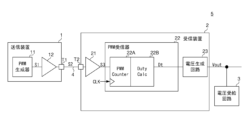
- FIG. 1 is a diagram showing a configuration of a voltage supply system according to a comparative example.
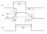
- FIG. 2 is a diagram showing an example of the waveforms of the PWM signals S1, S2, and S3.
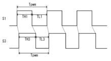
- FIG. 3 is a diagram showing an example of waveforms of several periods of the PWM signals S1 and S3.
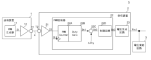
- FIG. 4 is a diagram showing a configuration of a voltage supply system according to the first embodiment of the present disclosure.
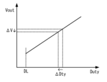
- FIG. 5 is a diagram showing a first example of the relationship between the duty during the high-level period and the voltage value of the output voltage.
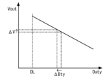
- FIG. 6 is a diagram showing a second example of the relationship between the duty during the high-level period and the voltage value of the output voltage.
- FIG. 5 is a diagram showing a first example of the relationship between the duty during the high-level period and the voltage value of the output voltage.
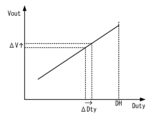
- FIG. 7 is a diagram showing a first example of the relationship between the duty during the low level period and the voltage value of the output voltage.
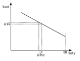
- FIG. 8 is a diagram showing a second example of the relationship between the duty during the low level period and the voltage value of the output voltage.
- FIG. 9 is a diagram showing a configuration of a voltage supply system according to the second embodiment of the present disclosure.
- FIG. 10 is a diagram showing a configuration of a voltage supply system according to the third embodiment of the present disclosure.
- FIG. 1 is a diagram showing the configuration of a voltage supply system 5 according to a comparative example.
- the voltage supply system 5 supplies an output voltage Vout to a voltage receiving circuit 3.
- the voltage receiving circuit 3 is, for example, a system-on-a-chip (SOC).
- the voltage supply system 5 includes a transmitting device 1 and a receiving device 2.
- the transmitting device 1 and the receiving device 2 are mounted on a printed circuit board (not shown).
- the transmitter 1 has an IC (integrated circuit) that includes an integrated PWM generator 11 and an output stage 12, and is configured as, for example, a CPU (Central Processing Unit).
- IC integrated circuit
- CPU Central Processing Unit
- the receiving device 2 has an IC that includes an input stage 21, a PWM receiver 22, and a voltage generating circuit 23 integrated together.
- the transmitting device 1 has a PWM output terminal T1 as an external terminal.
- the receiving device 2 has a PWM input terminal T2 as an external terminal.
- the PWM output terminal T1 and the PWM input terminal T2 are connected by wiring 4 on a printed circuit board.
- the PWM generator 11 generates a PWM signal S1 and outputs it to the output stage 12.
- the PWM signal S1 is a pulse signal that includes a high level and a low level.
- the output stage 12 outputs a PWM signal S2 based on the PWM signal S1, and transmits the PWM signal S2 through a transmission path that includes the PWM output terminal T1, the wiring 4, and the PWM input terminal T2.
- the PWM signal S2 transmitted through the transmission path is input to the input stage 21.
- the input stage 21 outputs a PWM signal S3 based on the PWM signal S2.
- the PWM signal S3 is input to the PWM receiver 22.
- the PWM receiver 22 has a PWM counter 22A and a duty calculation unit 22B.
- the PWM counter 22A counts the clock CLK of a predetermined frequency. For example, the PWM counter 22A obtains a count value corresponding to the high level period in one cycle of the PWM signal S3 and a count value corresponding to one cycle of the PWM signal S3. In this case, the duty calculation unit 22B calculates the duty of the high level period (the ratio of the high level period to one cycle) based on the obtained count values.
- the duty calculation unit 22B outputs data Dt indicating the calculated duty to the voltage generation circuit 23.
- the data Dt is n-bit (e.g., 8-bit) digital data.
- the voltage generation circuit 23 generates an output voltage Vout having a voltage value according to the data Dt. For example, the higher the duty calculated by the duty calculation unit 22B, the higher the voltage value of the output voltage Vout.
- the voltage supply system 5 can set the voltage value of the output voltage Vout by the duty of the PWM signal S1, and has a voltage adjustment function (VID (Voltage Identification)) using PWM.
- VID Voltage Identification
- FIG. 2 is a diagram showing example waveforms of the PWM signals S1, S2, and S3.
- the PWM signal S1 rises to a high level at timing t1
- the PWM signal S2 starts to rise
- the PWM signal S2 rises to a high level in the rise time Tr.
- the PWM signal S1 falls to a low level at timing t3
- the PWM signal S2 starts to fall
- the PWM signal S2 rises to a low level in the fall time Tf.
- the thresholds VIH and VIL shown in FIG. 2 are thresholds in the input stage 21. VIH>VIL.
- the PWM signal S3 rises to a high level.
- the PWM signal S3 falls to a low level. Due to the delay time D1 from time t1 to t2 and the delay time D2 from time t3 to t4, the high level period TH3 of the PWM signal S3 is longer than the high level period TH1 of the PWM signal S1.
- FIG. 3 is an example of waveforms showing several cycles of the PWM signals S1 and S3.
- one cycle Tpwm does not change for the PWM signals S1 and S3, but as described above, the high-level period TH3 of the PWM signal S3 is longer than the high-level period TH1 of the PWM signal S1.
- the duty of the low-level period is lower for the PWM signal S3 than for the PWM signal S1.
- the duty during the high-level period changes to a value higher in the receiving device 2 than the value assumed in the transmitting device 1, so that, for example, the voltage value of the output voltage Vout generated by the voltage generating circuit 23 becomes higher than the value assumed in the transmitting device 1.
- the reason for the change in duty as described above is a slowing down of the rise and fall of the PWM signal S2, which is due to the capacitance in the output stage 12, and the resistance and capacitance in the transmission path between the output stage 12 and the input stage 21. Note that if a noise reduction resistor element is connected between the PWM input terminal T2 and the input stage 21, the resistor element can also be a cause. The challenge is to suppress the effects of such PWM signal transmission errors.
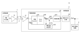
- FIG. 4 is a diagram showing a configuration of a voltage supply system 5 according to the first embodiment of the present disclosure.
- the configuration of Fig. 4 differs from the comparative example (Fig. 1) in that the PWM receiver 22 includes a data correction unit 22C and a limiting circuit 22D.
- the duty calculation unit 22B outputs data Dt1 indicating the calculated duty.
- the data correction unit 22C corrects the duty indicated by the data Dt1 using the correction amount ⁇ Dty, and outputs data Dt2 indicating the duty after correction.
- FIG. 5 is a diagram showing an example of the relationship between the duty during the high-level period and the voltage value of the output voltage Vout.
- the higher the duty during the high-level period the higher the voltage value of the output voltage Vout.
- the data correction unit 22C corrects the duty by subtracting the correction amount ⁇ Dty from the duty indicated by the data Dt1.
- the output voltage Vout can be corrected lower by the correction amount ⁇ V, and can be corrected to the voltage value assumed by the transmitter 1.
- the amount of change in the duty is constant regardless of the value of the duty
- the correction amount ⁇ Dty is constant regardless of the value of the duty.
- the corrected data Dt2 is input to the limiting circuit 22D. As shown in FIG. 5, if the duty falls below the lower limit DL when corrected with the correction amount ⁇ Dty, the limiting circuit 22D limits the corrected duty value to the lower limit DL. If the limiting circuit 22D limits the duty value, it outputs data Dt3 indicating the lower limit DL, and if not, it outputs the data Dt2 as is as data Dt3.
- the voltage generating circuit 23 generates an output voltage Vout having a voltage value corresponding to the data Dt3. This makes it possible to limit the voltage value to within the allowable range of voltage values in the voltage receiving circuit 3.
- FIG. 6 is a diagram showing another example of the relationship between the duty during the high-level period and the voltage value of the output voltage Vout.
- the higher the duty during the high-level period the lower the voltage value of the output voltage Vout.
- the data correction unit 22C corrects the voltage value by subtracting the correction amount ⁇ Dty from the duty indicated by the data Dt1.
- the output voltage Vout is corrected higher by the correction amount ⁇ V, and can be corrected to the assumed voltage value.
- the duty calculation unit 22B may calculate the duty Dty during the low-level period. In this case, if a transmission error occurs in the PWM signal, the duty Dty during the low-level period will be lower than the value assumed by the transmitting device 1. As shown in FIG. 7, if the voltage value of the output voltage Vout increases as the duty during the low-level period increases, the data correction unit 22C corrects the duty indicated by the data Dt1 by adding a correction amount ⁇ Dty. As a result, the output voltage Vout is corrected higher by the correction amount ⁇ V, and can be corrected to the expected value.
- the data correction unit 22C corrects the duty indicated by the data Dt1 by adding a correction amount ⁇ Dty. As a result, the output voltage Vout is corrected lower by the correction amount ⁇ V, and can be corrected to the expected value.
- the limiting circuit 22D limits the corrected duty value to the upper limit value DH. If the limiting circuit 22D limits the duty value, it outputs data Dt3 indicating the upper limit value DH, and if not, it outputs data Dt2 as is as data Dt3.
- Second embodiment> In the first embodiment described above, since the transmission path changes depending on the usage mode, the correction amount ⁇ Dty needs to be arbitrarily set by the user. Therefore, the second embodiment described next may be implemented.
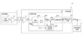
- FIG. 9 is a diagram showing the configuration of a voltage supply system 5 according to a second embodiment of the present disclosure.
- the difference between the configuration shown in FIG. 9 and the first embodiment (FIG. 4) is that the PWM receiver 22 has a correction amount determination unit 22E.
- the correction amount determination unit 22E determines the correction amount ⁇ Dty.
- the PWM generator 11 outputs a PWM signal S1 with a predetermined duty.
- the predetermined duty is a fixed value, for example, 50%.
- the PWM receiver 22 receives a PWM signal S3.
- data Dt1 indicating the calculated duty is generated, and the correction amount determination unit 22E acquires the generated data Dt1.
- the correction amount determination unit 22E determines the difference between the duty value indicated by the acquired data Dt1 and the above-mentioned predetermined duty (e.g., 50%) as the correction amount ⁇ Dty. Thereafter, the data correction unit 22C performs correction on the data Dt1 using the correction amount ⁇ Dty determined by the correction amount determination unit 22E.
- the predetermined duty e.g. 50%
- the correction amount ⁇ Dty can be automatically set according to the usage pattern of the transmission path.
- Fig. 10 is a diagram showing a configuration of a voltage supply system 5 according to a third embodiment of the present disclosure. The difference between the configuration shown in Fig. 10 and the second embodiment (Fig. 9) is that a duty setting value Sdty is input to a correction amount determination unit 22E.
- the duty setting value Sdty is variably set.
- a PWM signal S1 with a duty of the duty setting value Sdty is output from the PWM generator 11.
- the PWM receiver 22 receives a PWM signal S3.
- data Dt1 indicating the calculated duty is generated, and the correction amount determination unit 22E acquires the generated data Dt1.
- the correction amount determination unit 22E can determine the correction amount ⁇ Dty based on the difference between the duty value indicated by the acquired data Dt1 and the duty setting value Sdty.
- the duty setting value Sdty can be set within the allowable range of the specifications of the PWM generator 11 or the voltage receiving circuit 3, and the correction amount can be determined.
- the receiving device (2) includes: an input stage (21) configured to transmit and input a PWM signal (S1) transmitted from a transmitting device (1); A calculation unit (22B) configured to calculate the duty of the PWM signal based on the output (S3) of the input stage; a correction unit (22C) configured to perform correction by subtracting or adding a correction amount ( ⁇ Dty) to the calculated duty; (first configuration).
- the correction unit may further include a correction amount determination unit (22E) configured to determine the correction amount based on the difference between the duty calculated by the calculation unit (22B) when the PWM signal (S1) of a predetermined duty transmitted from the transmission device (1) is transmitted and input to the input stage (21) and the predetermined duty (second configuration).
- a correction amount determination unit (22E) configured to determine the correction amount based on the difference between the duty calculated by the calculation unit (22B) when the PWM signal (S1) of a predetermined duty transmitted from the transmission device (1) is transmitted and input to the input stage (21) and the predetermined duty (second configuration).
- the predetermined duty may be a fixed value (third configuration).
- the predetermined duty may be variably set (fourth configuration).
- a limiting circuit (22D) may be further provided that is configured to limit the duty after correction by the correction unit (22E) to a lower limit value (DL) if the duty falls below the lower limit value, or to limit the duty after correction by the correction unit to an upper limit value (DH) if the duty after correction by the correction unit exceeds the upper limit value (DH) (fifth configuration).
- the calculation unit (22B) is configured to calculate the duty indicating a ratio of a high-level period of the output (S3) of the input stage (21) to one cycle
- the correction section (22E) may be configured to perform correction by subtracting the correction amount from the calculated duty (sixth configuration).
- the calculation unit (22B) is configured to calculate the duty indicating a ratio of a low level period in the output (S3) of the input stage (21) to one cycle
- the correction section (22E) may be configured to perform correction by adding the correction amount to the calculated duty (seventh configuration).
- a voltage generating circuit (23) configured to generate an output voltage (Vout) having a voltage value according to the duty after correction by the correction unit (22E) may be further provided (eighth configuration).
- a voltage supply system (5) includes a receiving device (2) having a PWM input terminal (T2) configured to be able to receive and input the PWM signal;
- the transmitting device (1) has a PWM output terminal (T1) configured to transmit and output the PWM signal,
- the PWM output terminal and the PWM input terminal can be connected by wiring (4) on the board (ninth configuration).
- This disclosure can be used, for example, in voltage supply systems for various applications.
Landscapes
- Engineering & Computer Science (AREA)
- Power Engineering (AREA)
- Computer Networks & Wireless Communication (AREA)
- Signal Processing (AREA)
- Dc-Dc Converters (AREA)
Priority Applications (1)
| Application Number | Priority Date | Filing Date | Title |
|---|---|---|---|
| JP2025510717A JPWO2024203850A1 (cg-RX-API-DMAC7.html) | 2023-03-29 | 2024-03-22 |
Applications Claiming Priority (2)
| Application Number | Priority Date | Filing Date | Title |
|---|---|---|---|
| JP2023052949 | 2023-03-29 | ||
| JP2023-052949 | 2023-03-29 |
Publications (1)
| Publication Number | Publication Date |
|---|---|
| WO2024203850A1 true WO2024203850A1 (ja) | 2024-10-03 |
Family
ID=92906395
Family Applications (1)
| Application Number | Title | Priority Date | Filing Date |
|---|---|---|---|
| PCT/JP2024/011298 Ceased WO2024203850A1 (ja) | 2023-03-29 | 2024-03-22 | 受信装置、および電圧供給システム |
Country Status (2)
| Country | Link |
|---|---|
| JP (1) | JPWO2024203850A1 (cg-RX-API-DMAC7.html) |
| WO (1) | WO2024203850A1 (cg-RX-API-DMAC7.html) |
Citations (2)
| Publication number | Priority date | Publication date | Assignee | Title |
|---|---|---|---|---|
| JP2014157784A (ja) * | 2013-02-18 | 2014-08-28 | Mitsubishi Electric Corp | 光源点灯装置およびこれを用いた照明装置 |
| WO2023276265A1 (ja) * | 2021-07-01 | 2023-01-05 | 日立Astemo株式会社 | インバータ制御装置、計算方法 |
-
2024
- 2024-03-22 JP JP2025510717A patent/JPWO2024203850A1/ja active Pending
- 2024-03-22 WO PCT/JP2024/011298 patent/WO2024203850A1/ja not_active Ceased
Patent Citations (2)
| Publication number | Priority date | Publication date | Assignee | Title |
|---|---|---|---|---|
| JP2014157784A (ja) * | 2013-02-18 | 2014-08-28 | Mitsubishi Electric Corp | 光源点灯装置およびこれを用いた照明装置 |
| WO2023276265A1 (ja) * | 2021-07-01 | 2023-01-05 | 日立Astemo株式会社 | インバータ制御装置、計算方法 |
Also Published As
| Publication number | Publication date |
|---|---|
| JPWO2024203850A1 (cg-RX-API-DMAC7.html) | 2024-10-03 |
Similar Documents
| Publication | Publication Date | Title |
|---|---|---|
| KR100871828B1 (ko) | 히스테리시스 특성을 이용한 싱글 슬로프 adc와 그 변환 방법, 및 상기 싱글 슬로프 adc를 구비하는 cmos 이미지 센서 | |
| US10394749B2 (en) | Asynchronous transceiver for on-vehicle electronic device | |
| US7778349B2 (en) | Method and transmission apparatus for transmitting a bivalent signal | |
| US7667534B2 (en) | Control interface and protocol | |
| JP2007097176A (ja) | 信号検出回路 | |
| EP3648426A1 (en) | Integrated circuit and method for communicating data | |
| US9929671B2 (en) | Power converter in powered device of power-over-ethernet system and control method thereof | |
| US8928421B2 (en) | Control circuit for reducing electromagnetic interference | |
| US10469243B2 (en) | Communication apparatus, replacement unit, and image forming apparatus | |
| JP7695762B2 (ja) | 送受信回路、方法 | |
| US9075590B2 (en) | Voltage identification definition reference voltage generation circuit and boot voltage generating method thereof | |
| JP5488074B2 (ja) | パルス幅変調信号生成回路 | |
| JP4398475B2 (ja) | クロックのデューティ補正回路 | |
| TWI657662B (zh) | 信號介面系統及其資料傳送方法 | |
| CN110690689B (zh) | 过电流保护装置及方法 | |
| JP4894919B2 (ja) | 中継回路、情報処理装置、中継方法 | |
| JP2010057150A (ja) | 協動回路 | |
| US20100019819A1 (en) | Delay Circuit | |
| JP4988425B2 (ja) | 受信回路 | |
| US6940340B2 (en) | Noise-proof bus circuit | |
| JP2008058294A (ja) | パルス幅変調信号のレベル測定装置およびレベル測定方法 | |
| JP2009268184A (ja) | Ac検出回路および直流電源装置 | |
| JP2012205041A (ja) | インターフェース回路 | |
| JP6451196B2 (ja) | 通信装置 | |
| JPH10200586A (ja) | データ信号伝送方法および半導体装置の信号入力回路 |
Legal Events
| Date | Code | Title | Description |
|---|---|---|---|
| 121 | Ep: the epo has been informed by wipo that ep was designated in this application |
Ref document number: 24779968 Country of ref document: EP Kind code of ref document: A1 |
|
| ENP | Entry into the national phase |
Ref document number: 2025510717 Country of ref document: JP Kind code of ref document: A |
|
| WWE | Wipo information: entry into national phase |
Ref document number: 2025510717 Country of ref document: JP |
|
| NENP | Non-entry into the national phase |
Ref country code: DE |
|
| 122 | Ep: pct application non-entry in european phase |
Ref document number: 24779968 Country of ref document: EP Kind code of ref document: A1 |