WO2024203285A1 - 窒化物半導体装置 - Google Patents
窒化物半導体装置 Download PDFInfo
- Publication number
- WO2024203285A1 WO2024203285A1 PCT/JP2024/009572 JP2024009572W WO2024203285A1 WO 2024203285 A1 WO2024203285 A1 WO 2024203285A1 JP 2024009572 W JP2024009572 W JP 2024009572W WO 2024203285 A1 WO2024203285 A1 WO 2024203285A1
- Authority
- WO
- WIPO (PCT)
- Prior art keywords
- opening
- layer
- gate
- nitride semiconductor
- semiconductor device
- Prior art date
- Legal status (The legal status is an assumption and is not a legal conclusion. Google has not performed a legal analysis and makes no representation as to the accuracy of the status listed.)
- Ceased
Links
Images












Classifications
-
- H—ELECTRICITY
- H10—SEMICONDUCTOR DEVICES; ELECTRIC SOLID-STATE DEVICES NOT OTHERWISE PROVIDED FOR
- H10D—INORGANIC ELECTRIC SEMICONDUCTOR DEVICES
- H10D30/00—Field-effect transistors [FET]
- H10D30/40—FETs having zero-dimensional [0D], one-dimensional [1D] or two-dimensional [2D] charge carrier gas channels
- H10D30/47—FETs having zero-dimensional [0D], one-dimensional [1D] or two-dimensional [2D] charge carrier gas channels having two-dimensional [2D] charge carrier gas channels, e.g. nanoribbon FETs or high electron mobility transistors [HEMT]
- H10D30/471—High electron mobility transistors [HEMT] or high hole mobility transistors [HHMT]
- H10D30/475—High electron mobility transistors [HEMT] or high hole mobility transistors [HHMT] having wider bandgap layer formed on top of lower bandgap active layer, e.g. undoped barrier HEMTs such as i-AlGaN/GaN HEMTs
-
- H—ELECTRICITY
- H10—SEMICONDUCTOR DEVICES; ELECTRIC SOLID-STATE DEVICES NOT OTHERWISE PROVIDED FOR
- H10D—INORGANIC ELECTRIC SEMICONDUCTOR DEVICES
- H10D62/00—Semiconductor bodies, or regions thereof, of devices having potential barriers
- H10D62/10—Shapes, relative sizes or dispositions of the regions of the semiconductor bodies; Shapes of the semiconductor bodies
- H10D62/102—Constructional design considerations for preventing surface leakage or controlling electric field concentration
-
- H—ELECTRICITY
- H10—SEMICONDUCTOR DEVICES; ELECTRIC SOLID-STATE DEVICES NOT OTHERWISE PROVIDED FOR
- H10D—INORGANIC ELECTRIC SEMICONDUCTOR DEVICES
- H10D62/00—Semiconductor bodies, or regions thereof, of devices having potential barriers
- H10D62/10—Shapes, relative sizes or dispositions of the regions of the semiconductor bodies; Shapes of the semiconductor bodies
- H10D62/17—Semiconductor regions connected to electrodes not carrying current to be rectified, amplified or switched, e.g. channel regions
- H10D62/343—Gate regions of field-effect devices having PN junction gates
-
- H—ELECTRICITY
- H10—SEMICONDUCTOR DEVICES; ELECTRIC SOLID-STATE DEVICES NOT OTHERWISE PROVIDED FOR
- H10D—INORGANIC ELECTRIC SEMICONDUCTOR DEVICES
- H10D62/00—Semiconductor bodies, or regions thereof, of devices having potential barriers
- H10D62/80—Semiconductor bodies, or regions thereof, of devices having potential barriers characterised by the materials
- H10D62/83—Semiconductor bodies, or regions thereof, of devices having potential barriers characterised by the materials being Group IV materials, e.g. B-doped Si or undoped Ge
-
- H—ELECTRICITY
- H10—SEMICONDUCTOR DEVICES; ELECTRIC SOLID-STATE DEVICES NOT OTHERWISE PROVIDED FOR
- H10D—INORGANIC ELECTRIC SEMICONDUCTOR DEVICES
- H10D64/00—Electrodes of devices having potential barriers
- H10D64/111—Field plates
-
- H—ELECTRICITY
- H10—SEMICONDUCTOR DEVICES; ELECTRIC SOLID-STATE DEVICES NOT OTHERWISE PROVIDED FOR
- H10D—INORGANIC ELECTRIC SEMICONDUCTOR DEVICES
- H10D64/00—Electrodes of devices having potential barriers
- H10D64/111—Field plates
- H10D64/112—Field plates comprising multiple field plate segments
-
- H—ELECTRICITY
- H10—SEMICONDUCTOR DEVICES; ELECTRIC SOLID-STATE DEVICES NOT OTHERWISE PROVIDED FOR
- H10D—INORGANIC ELECTRIC SEMICONDUCTOR DEVICES
- H10D64/00—Electrodes of devices having potential barriers
- H10D64/20—Electrodes characterised by their shapes, relative sizes or dispositions
-
- H—ELECTRICITY
- H10—SEMICONDUCTOR DEVICES; ELECTRIC SOLID-STATE DEVICES NOT OTHERWISE PROVIDED FOR
- H10D—INORGANIC ELECTRIC SEMICONDUCTOR DEVICES
- H10D64/00—Electrodes of devices having potential barriers
- H10D64/20—Electrodes characterised by their shapes, relative sizes or dispositions
- H10D64/23—Electrodes carrying the current to be rectified, amplified, oscillated or switched, e.g. sources, drains, anodes or cathodes
-
- H—ELECTRICITY
- H10—SEMICONDUCTOR DEVICES; ELECTRIC SOLID-STATE DEVICES NOT OTHERWISE PROVIDED FOR
- H10D—INORGANIC ELECTRIC SEMICONDUCTOR DEVICES
- H10D64/00—Electrodes of devices having potential barriers
- H10D64/20—Electrodes characterised by their shapes, relative sizes or dispositions
- H10D64/27—Electrodes not carrying the current to be rectified, amplified, oscillated or switched, e.g. gates
-
- H—ELECTRICITY
- H10—SEMICONDUCTOR DEVICES; ELECTRIC SOLID-STATE DEVICES NOT OTHERWISE PROVIDED FOR
- H10D—INORGANIC ELECTRIC SEMICONDUCTOR DEVICES
- H10D62/00—Semiconductor bodies, or regions thereof, of devices having potential barriers
- H10D62/10—Shapes, relative sizes or dispositions of the regions of the semiconductor bodies; Shapes of the semiconductor bodies
- H10D62/124—Shapes, relative sizes or dispositions of the regions of semiconductor bodies or of junctions between the regions
- H10D62/126—Top-view geometrical layouts of the regions or the junctions
- H10D62/127—Top-view geometrical layouts of the regions or the junctions of cellular field-effect devices, e.g. multicellular DMOS transistors or IGBTs
-
- H—ELECTRICITY
- H10—SEMICONDUCTOR DEVICES; ELECTRIC SOLID-STATE DEVICES NOT OTHERWISE PROVIDED FOR
- H10D—INORGANIC ELECTRIC SEMICONDUCTOR DEVICES
- H10D62/00—Semiconductor bodies, or regions thereof, of devices having potential barriers
- H10D62/80—Semiconductor bodies, or regions thereof, of devices having potential barriers characterised by the materials
- H10D62/82—Heterojunctions
- H10D62/824—Heterojunctions comprising only Group III-V materials heterojunctions, e.g. GaN/AlGaN heterojunctions
-
- H—ELECTRICITY
- H10—SEMICONDUCTOR DEVICES; ELECTRIC SOLID-STATE DEVICES NOT OTHERWISE PROVIDED FOR
- H10D—INORGANIC ELECTRIC SEMICONDUCTOR DEVICES
- H10D62/00—Semiconductor bodies, or regions thereof, of devices having potential barriers
- H10D62/80—Semiconductor bodies, or regions thereof, of devices having potential barriers characterised by the materials
- H10D62/85—Semiconductor bodies, or regions thereof, of devices having potential barriers characterised by the materials being Group III-V materials, e.g. GaAs
- H10D62/8503—Nitride Group III-V materials, e.g. AlN or GaN
Definitions
- This disclosure relates to nitride semiconductor devices.
- nitride semiconductors such as gallium nitride (GaN)
- GaN gallium nitride
- a nitride semiconductor device having such a configuration includes, for example, an electron transit layer, an electron supply layer formed on the electron transit layer and having a larger band gap than the electron transit layer, a gate layer formed on the electron transit layer and containing acceptor-type impurities, a gate electrode formed on the gate layer, and a passivation layer covering the electron supply layer, gate layer, and gate electrode.
- This nitride semiconductor device also includes a field plate electrode that is integrated with the source electrode and extends from the source electrode across the gate layer and gate electrode toward the drain electrode.
- parasitic capacitance may occur due to the field plate electrode. This parasitic capacitance may adversely affect switching responsiveness.
- a nitride semiconductor device includes an electron transport layer made of a nitride semiconductor, an electron supply layer formed on the electron transport layer and made of a nitride semiconductor having a band gap larger than that of the electron transport layer, a gate layer formed on the electron supply layer and made of a nitride semiconductor containing an acceptor-type impurity, a gate electrode formed on the gate layer, and a passivation layer covering the electron supply layer, the gate layer, and the gate electrode, the passivation layer having a first opening and a second opening spaced apart in a first direction, and the gate layer being located between the first opening and the second opening.
- the semiconductor device includes a source electrode that contacts the electron supply layer through a first opening, a drain electrode that contacts the electron supply layer through the second opening, and a field plate electrode that is formed on the passivation layer and is electrically connected to the source electrode, the field plate electrode including a plate extension that extends in a region between the gate layer and the drain electrode in a plan view and faces the electron supply layer through the passivation layer, and an opening is formed in the field plate electrode, and the opening is formed in at least one of the plate extension and a position that overlaps with the gate layer in a plan view.
- the nitride semiconductor device can reduce the parasitic capacitance caused by the field plate electrode.
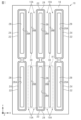
- FIG. 1 is an illustrative schematic plan view of a nitride semiconductor device according to the first embodiment.
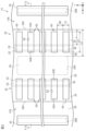
- FIG. 2 is an enlarged view of the dashed-dotted frame A1 in FIG. 1, and is a schematic plan view in which a passivation layer and a field plate electrode are added to the nitride semiconductor device in FIG.
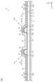
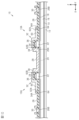
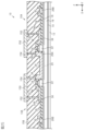
- FIG. 3 is a schematic cross-sectional view of the nitride semiconductor device taken along line F3-F3 in FIG.
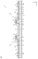
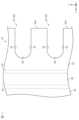
- FIG. 4 is a schematic cross-sectional view of the nitride semiconductor device taken along line F4-F4 in FIG.
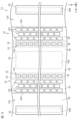
- FIG. 5 is a schematic plan view showing an enlargement of the dashed-dotted frame A2 in FIG. FIG.
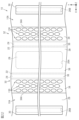
- FIG. 6 is a schematic plan view showing an enlargement of the dashed-dotted frame A2 in FIG. 2, which shows the state of the depletion layer when a drain-source voltage is applied.
- FIG. 7 is a schematic enlarged plan view of a field plate electrode and its periphery in the nitride semiconductor device according to the second embodiment.
- FIG. 8 is a schematic cross-sectional view of the nitride semiconductor device taken along line F8-F8 in FIG.
- FIG. 9 is a schematic enlarged plan view of a field plate electrode and its periphery in the nitride semiconductor device according to the third embodiment.
- FIG. 10 is a schematic cross-sectional view of the nitride semiconductor device taken along line F10-F10 in FIG. FIG.
- FIG. 11 is a schematic plan view showing an opening of a field plate electrode and its periphery in a modified nitride semiconductor device, on an enlarged scale.
- FIG. 12 is a schematic enlarged plan view of an opening in a field plate electrode and its periphery in a nitride semiconductor device according to a modified example.
- FIG. 13 is a schematic plan view showing an enlarged view of an opening in a field plate electrode and its periphery in a nitride semiconductor device according to a modified example.
- FIG. 14 is a schematic plan view showing an enlarged view of an opening in a field plate electrode and its periphery in a nitride semiconductor device according to a modified example.
- FIG. 12 is a schematic enlarged plan view of an opening in a field plate electrode and its periphery in a nitride semiconductor device according to a modified example.
- FIG. 13 is a schematic plan view showing an enlarged view of an opening in a field plate electrode and
- FIG. 15 is a schematic enlarged plan view of a field plate electrode and its periphery in a nitride semiconductor device according to a modified example.
- FIG. 16 is a schematic enlarged plan view of a field plate electrode and its periphery in a nitride semiconductor device according to a modified example.
- FIG. 17 is a schematic enlarged plan view of a field plate electrode and its periphery in a nitride semiconductor device according to a modified example.
- FIG. 18 is a schematic enlarged plan view of a field plate electrode and its periphery in a nitride semiconductor device according to a modified example.
- FIG. 16 is a schematic enlarged plan view of a field plate electrode and its periphery in a nitride semiconductor device according to a modified example.
- FIG. 17 is a schematic enlarged plan view of a field plate electrode and its periphery in a nitride semiconductor device according to a modified example.
- FIG. 19 is a schematic enlarged plan view of a field plate electrode and its periphery in a nitride semiconductor device according to a modified example.
- FIG. 20 is a schematic enlarged plan view of a field plate electrode and its periphery in a nitride semiconductor device according to a modified example.
- FIG. 21 is a schematic enlarged plan view of a field plate electrode and its periphery in a nitride semiconductor device according to a modified example.
- FIG. 22 is a schematic enlarged plan view of a field plate electrode and its periphery in a nitride semiconductor device according to a modified example.
- FIG. 20 is a schematic enlarged plan view of a field plate electrode and its periphery in a nitride semiconductor device according to a modified example.
- FIG. 21 is a schematic enlarged plan view of a field plate electrode and its periphery in a nitride semiconductor device according to a modified example.
- FIG. 23 is a schematic enlarged plan view of a field plate electrode and its periphery in a nitride semiconductor device according to a modified example.
- FIG. 24 is a schematic enlarged plan view of a field plate electrode and its periphery in a nitride semiconductor device according to a modified example.
- FIG. 25 is a schematic cross-sectional view of the nitride semiconductor device taken along line F25-F25 in FIG.
- FIG. 26 is a schematic cross-sectional view of a nitride semiconductor device according to a modified example.
- FIG. 27 is a schematic cross-sectional view of a nitride semiconductor device according to a modified example.
- statements such as “the dimensions (width, depth, length, distance) of part A are equal to the dimensions (width, depth, length, distance) of part B" or “the dimensions (width, depth, length, distance) of part A and the dimensions (width, depth, length, distance) of part B are equal to each other” mean that the absolute value of the difference between the dimensions (width, depth, length, distance) of part A and the dimensions (width, depth, length, distance) of part B is within 10% of the dimensions (width, depth, length, distance) of part A, for example.
- Figure 1 shows a schematic planar structure of the nitride semiconductor device 10.
- Figure 2 shows a schematic enlarged planar structure of a portion of the nitride semiconductor device 10 in Figure 1.
- Figure 3 shows a schematic cross-sectional structure of the nitride semiconductor device 10 in Figure 2 taken along line F3-F3.
- the nitride semiconductor device 10 is configured as a high electron mobility transistor (HEMT) using a nitride semiconductor.
- HEMT high electron mobility transistor
- examples of the nitride semiconductor that can be used include gallium nitride (GaN), aluminum nitride (AlN), and indium nitride (InN), and can generally be expressed as Al x In y Ga 1-x-y N (0 ⁇ x ⁇ 1, 0 ⁇ y ⁇ 1, 0 ⁇ x+y ⁇ 1).
- planar view refers to viewing an object (nitride semiconductor device 10 or a component thereof) in the Z direction of the mutually orthogonal XYZ axes shown in each figure, unless otherwise expressly stated.
- a nitride semiconductor device 10 includes a plurality of unit transistors 10A having a HEMT structure using a nitride semiconductor.
- a nitride semiconductor device 10 includes a plurality of unit transistors 10A having a HEMT structure using a nitride semiconductor.
- the unit transistor 10A (nitride semiconductor device 10) includes a semiconductor substrate 12, a buffer layer 14 formed on the semiconductor substrate 12, an electron transit layer 16 formed on the buffer layer 14, and an electron supply layer 18 formed on the electron transit layer 16.
- the semiconductor substrate 12 may be formed of silicon (Si), silicon carbide (SiC), GaN, sapphire, or other substrate materials.
- the semiconductor substrate 12 may be a Si substrate.
- the thickness of the semiconductor substrate 12 may be, for example, 200 ⁇ m or more and 1500 ⁇ m or less.
- the buffer layer 14 may be located between the semiconductor substrate 12 and the electron transport layer 16.
- the buffer layer 14 may be composed of any material that can facilitate epitaxial growth of the electron transport layer 16.
- the buffer layer 14 may include one or more nitride semiconductor layers.
- the buffer layer 14 may include at least one of an AlN layer, an aluminum gallium nitride (AlGaN) layer, and a graded AlGaN layer having different aluminum (Al) compositions.
- the buffer layer 14 may be composed of a single AlN layer, a single AlGaN layer, a layer having an AlGaN/GaN superlattice structure, a layer having an AlN/AlGaN superlattice structure, or a layer having an AlN/GaN superlattice structure.
- impurities may be introduced into a portion of the buffer layer 14 to make the buffer layer 14 semi-insulating.
- the impurity may be, for example, carbon (C) or iron (Fe), and the concentration of the impurity may be, for example, 4 ⁇ 10 16 cm ⁇ 3 or more.
- the electron travel layer 16 is made of a nitride semiconductor.
- the electron travel layer 16 is, for example, a GaN layer.
- the thickness of the electron travel layer 16 is, for example, 0.5 ⁇ m or more and 2 ⁇ m or less.
- an impurity may be introduced into a part of the electron travel layer 16 to make the electron travel layer 16 semi-insulating except for the surface layer region.
- the impurity is, for example, C
- the peak concentration of the impurity in the electron travel layer 16 is, for example, 1 ⁇ 10 19 cm ⁇ 3 or more.
- the electron supply layer 18 is made of a nitride semiconductor having a larger band gap than the electron transit layer 16.
- the electron supply layer 18 is, for example, an AlGaN layer.
- the electron supply layer 18 is made of Al x Ga 1-x N, where x is 0.1 ⁇ x ⁇ 0.4, and more preferably 0.2 ⁇ x ⁇ 0.3.
- the thickness of the electron supply layer 18 is, for example, 5 nm or more and 20 nm or less.
- the electron transit layer 16 and the electron supply layer 18 are composed of nitride semiconductors having different lattice constants. Therefore, the nitride semiconductor (e.g., GaN) constituting the electron transit layer 16 and the nitride semiconductor (e.g., AlGaN) constituting the electron supply layer 18 form a lattice-mismatched heterojunction.
- the energy level of the conduction band of the electron transit layer 16 near the heterojunction interface is lower than the Fermi level due to spontaneous polarization of the electron transit layer 16 and the electron supply layer 18 and piezoelectric polarization caused by stress experienced by the electron supply layer 18 near the heterojunction interface.
- 2DEG two-dimensional electron gas
- the unit transistor 10A (nitride semiconductor device 10) further includes a gate layer 22 formed on the electron supply layer 18, a gate electrode 24 formed on the gate layer 22, and a passivation layer 26.
- the passivation layer 26 is formed on the electron supply layer 18, the gate layer 22, and the gate electrode 24, and includes a first opening 26A and a second opening 26B.
- the first opening 26A and the second opening 26B are spaced apart in the X direction.
- the nitride semiconductor device 10 further includes a source electrode 28 that contacts the electron supply layer 18 through the first opening 26A, and a drain electrode 30 that contacts the electron supply layer 18 through the second opening 26B.
- the X direction corresponds to the "first direction".
- the gate layer 22 is located between the first opening 26A and the second opening 26B of the passivation layer 26, and is spaced apart from each of the first opening 26A and the second opening 26B. The gate layer 22 is located closer to the first opening 26A than to the second opening 26B.
- the gate layer 22 has a band gap smaller than that of the electron supply layer 18 and is composed of a nitride semiconductor containing an acceptor-type impurity.
- the gate layer 22 may be composed of any material having a band gap smaller than that of the electron supply layer 18, which is, for example, an AlGaN layer.
- the gate layer 22 is a GaN layer doped with an acceptor-type impurity (a p-type GaN layer).
- the acceptor-type impurity may include at least one of zinc (Zn), magnesium (Mg), and C.
- the maximum concentration of the acceptor-type impurity in the gate layer 22 is, for example, 1 ⁇ 10 18 cm ⁇ 3 or more and 1 ⁇ 10 20 cm ⁇ 3 or less.
- the energy levels of the electron transit layer 16 and the electron supply layer 18 are raised by the inclusion of acceptor-type impurities in the gate layer 22. Therefore, in the region directly below the gate layer 22, the energy level of the conduction band of the electron transit layer 16 near the heterojunction interface between the electron transit layer 16 and the electron supply layer 18 is approximately the same as or higher than the Fermi level. Therefore, at zero bias when no voltage is applied to the gate electrode 24, 2DEG 20 is not formed in the electron transit layer 16 in the region directly below the gate layer 22. On the other hand, 2DEG 20 is formed in the electron transit layer 16 in regions other than the region directly below the gate layer 22.
- the presence of the gate layer 22 doped with acceptor-type impurities causes the 2DEG 20 to disappear in the region directly below the gate layer 22.
- the transistor operates normally off.
- an appropriate on-voltage is applied to the gate electrode 24, a channel is formed by the 2DEG 20 in the electron transit layer 16 in the region directly below the gate electrode 24, providing electrical continuity between the source and drain.
- the gate electrode 24 is composed of one or more metal layers.
- the gate electrode 24 is a titanium nitride (TiN) layer.
- the gate electrode 24 may be composed of a first metal layer formed of a material containing Ti and a second metal layer formed of a material containing TiN and stacked on the first metal layer.
- the gate electrode 24 can form a Schottky junction with the gate layer 22.
- the gate electrode 24 can be formed in an area smaller than the gate layer 22 in a plan view.
- the thickness of the gate electrode 24 is, for example, 50 nm or more and 200 nm or less.
- the passivation layer 26 is formed on the electron supply layer 18.
- the passivation layer 26 covers the electron supply layer 18, the gate layer 22, and the gate electrode 24.
- the passivation layer 26 may be made of a material containing any one of silicon nitride (SiN), silicon dioxide (SiO 2 ), silicon oxynitride (SiON), alumina (Al 2 O 3 ), AlN, and aluminum oxynitride (AlON).
- the thickness of the passivation layer 26 is thicker than the thickness of the electron supply layer 18.
- the thickness of the passivation layer 26 is, for example, 300 nm or more and 1000 nm or less.
- the thickness of the passivation layer 26 can be changed arbitrarily.
- the source electrode 28 and the drain electrode 30 are disposed on the upper surface of the electron supply layer 18 so as to sandwich the gate layer 22.
- the source electrode 28 and the drain electrode 30 may be formed of one or more metal layers.
- the source electrode 28 and the drain electrode 30 may be formed of a combination of two or more metal layers selected from a group including a Ti layer, a TiN layer, an Al layer, an AlSiCu layer, and an AlCu layer.
- At least a portion of the source electrode 28 is filled in the first opening 26A and is in ohmic contact with the 2DEG 20 directly below the electron supply layer 18 through the first opening 26A.
- at least a portion of the drain electrode 30 is filled in the second opening 26B and is in ohmic contact with the 2DEG 20 directly below the electron supply layer 18 through the second opening 26B.
- the unit transistor 10A (nitride semiconductor device 10) further includes a field plate electrode 32 electrically connected to the source electrode 28.
- the field plate electrode 32 is integrated with the source electrode 28.
- the field plate electrode 32 serves to reduce electric field concentration near the end of the gate electrode 24 and near the end of the gate layer 22 when a drain voltage is applied to the drain electrode 30 in a zero bias state where no gate voltage is applied to the gate electrode 24.
- the detailed configuration of the field plate electrode 32 will be described later.
- FIG. 1 shows the planar structures of the contact portions of both the source electrode 28 and the drain electrode 30 that contact the electron supply layer 18.
- the nitride semiconductor device 10 includes a plurality of source electrodes 28 arranged side by side in the X and Y directions in a plan view on the electron supply layer 18.
- a total of six source electrodes 28 are arranged at a distance from each other in three rows in the X direction and two rows in the Y direction.
- Each source electrode 28 is formed in a strip shape extending in the Y direction in a plan view.
- the nitride semiconductor device 10 also includes a plurality of drain electrodes 30 arranged side by side in the X and Y directions in plan view on the electron supply layer 18.
- a total of four drain electrodes 30 are arranged at a distance from each other, in two rows in the X direction and two rows in the Y direction.
- Each drain electrode 30 is formed in a strip shape extending in the Y direction in plan view.
- the plurality of drain electrodes 30 and the plurality of source electrodes 28 are arranged alternately one by one in the X direction. In this case, for example, a source electrode 28 is located at both ends in the X direction.
- the nitride semiconductor device 10 also includes a plurality of gate layers 22 and a plurality of gate electrodes 24 arranged side by side in the X and Y directions in a plan view on the electron supply layer 18.
- a total of six gate layers 22 and gate electrodes 24 are arranged in three rows in the X direction and two rows in the Y direction.
- Each gate layer 22 and each gate electrode 24 extends in the Y direction and surrounds one of the source electrodes 28 in a plan view. That is, each gate layer 22 and each gate electrode 24 is formed in a ring shape.
- annular refers not only to any structure that is continuous without ends, i.e., that forms a loop, but also to structures that have a shape with a break (gap), such as a C-shape.
- Such “annular” shapes include not only ovals, but also any shape that includes multiple corners with a specified angle, such as a right angle, or rounded corners.
- Figure 2 shows a schematic planar structure of the nitride semiconductor device 10 in a region enclosed by a dashed line frame A1 in Figure 1.
- Figure 2 shows a schematic planar structure in which a passivation layer 26 and a field plate electrode 32 are added to Figure 1, and a part in the Y direction is omitted in order to enlarge the figure.
- Figure 4 shows a schematic cross-sectional structure of the nitride semiconductor device 10 cut along line F4-F4 in Figure 2.
- Figures 5 and 6 show schematic planar structures in which the region enclosed by a dashed line frame A2 in Figure 2 is enlarged.
- the field plate electrode 32 is disposed between two drain electrodes 30 that are spaced apart in the X direction.
- the field plate electrode 32 is formed in a rectangular shape in a plan view.
- the field plate electrode 32 is provided on both sides of the source electrode 28 in the X direction.
- the field plate electrode 32 extends into the region between the gate layer 22 and the drain electrode 30 in a plan view.
- the field plate electrode 32 is formed on the passivation layer 26.
- the field plate electrode 32 includes a plate extension portion 34 that faces the electron supply layer 18 through the passivation layer 26, and a gate opposing portion 36 that faces the gate layer 22 through the passivation layer 26.
- the field plate electrode 32 also includes a source connection portion 38 that faces the electron supply layer 18 through the passivation layer 26 at a position closer to the source electrode 28 than the gate opposing portion 36.
- the plate extension portion 34, the gate opposing portion 36, and the source connection portion 38 are integrated.
- the plate extension portion 34 is provided on the opposite side of the gate opposing portion 36 to the source electrode 28 in the X direction.
- the plate extension portion 34 is provided closer to the drain electrode 30 than the gate opposing portion 36 in the X direction.
- the plate extension portion 34 is also separated from the drain electrode 30 in the X direction.
- the gate facing portion 36 faces the gate electrode 24 via the passivation layer 26.
- the plate extension 34 has a plate tip surface 34A that faces the drain electrode 30 in a plan view.
- the plate tip surface 34A extends along the Y direction in a plan view.
- the plate tip surface 34A is disposed between the gate layer 22 and the drain electrode 30 in the X direction.
- the X-direction length of the field plate electrode 32 is set according to the X-direction position of the plate tip surface 34A.
- the length of the field plate electrode 32 is set appropriately according to the switching speed and withstand voltage required of the nitride semiconductor device 10.
- the X-direction position of the plate tip surface 34A is set appropriately according to the switching speed and withstand voltage required of the nitride semiconductor device 10.
- the gate opposing portion 36 is formed by a region of the field plate electrode 32 that overlaps with the gate layer 22 in a planar view. Therefore, in a planar view, the length in the X direction of the gate opposing portion 36 is shorter than the length in the X direction of the plate extension portion 34. In a planar view, the length in the X direction of the gate opposing portion 36 is equal to the width (length in the X direction) of the gate layer 22 extending in the Y direction.
- the source connection portion 38 is formed by the region of the field plate electrode 32 between the source electrode 28 and the gate opposing portion 36 in the X direction.
- the source electrode 28 is formed by the portion that is in contact with the electron supply layer 18. Therefore, it can be said that the source connection portion 38 is formed by the region of the field plate electrode 32 between the first opening 26A and the gate opposing portion 36 in the X direction in a plan view.
- an opening 40 is formed in the field plate electrode 32.
- at least a portion of the opening 40 is formed in the plate extension portion 34.
- the opening 40 is disposed in the plate extension portion 34.
- the opening 40 is not formed in the gate facing portion 36.
- the opening 40 is a recess 42 recessed from the plate tip surface 34A toward the gate layer 22.
- the recess 42 extends with the Y direction as its width direction and the X direction as its depth direction.
- the recess 42 is open toward the drain electrode 30.
- multiple recesses 42 are arranged spaced apart in the Y direction.
- the multiple recesses 42 are arranged, for example, at an equal pitch.
- the widths of the multiple recesses 42 are equal to each other.
- the depths of the multiple recesses 42 are also equal to each other.
- the recess 42 includes a pair of side surfaces 44 and a bottom surface 46 connecting the pair of side surfaces 44.
- the pair of side surfaces 44 are spaced apart from each other in the Y direction.
- Each side surface 44 extends along the X direction in a plan view. Therefore, the pair of side surfaces 44 are parallel to each other.
- the width of the recess 42 in the Y direction is the same from the opening at the plate tip surface 34A of the plate extension portion 34 to the bottom surface 46.
- the bottom surface 46 of the recess 42 is disposed closer to the drain electrode 30 than the side surface 22X of the gate layer 22 in the X direction.
- the position of the bottom surface 46 in the X direction i.e., the depth H of the recess 42, is appropriately set in accordance with the required switching speed of the nitride semiconductor device 10, in a range closer to the drain electrode 30 than the side surface 22X of the gate layer 22 in the X direction.
- the depth H can be defined as the distance in the X direction from the plate tip surface 34A to the bottom surface 46 of the recess 42 in a plan view.
- the depth H of the recess 42 in a plan view is deeper than the width W of the recess 42. In one example, the depth H of the recess 42 in a plan view is deeper than 1/2 the length L of the plate extension 34 in the X direction.
- the length L of the plate extension 34 in the X direction can be defined as the distance in the X direction from the side closest to the plate tip surface 34A of both side surfaces of the gate layer 22 in the X direction to the plate tip surface 34A in a plan view.
- the width W of the recesses 42 is equal to the distance D between the recesses 42.
- the distance D between the recesses 42 can be defined as the distance in the Y direction between the side 44 of one recess 42 that is closer to the other recess 42 and the side 44 of the other recess 42 that is closer to the one recess 42.
- the two-dot chain line in FIG. 6 indicates the depletion layer formed in the field plate electrode 32 when a drain-source voltage is applied.
- the distance between a pair of side surfaces 44 in the X direction i.e., the width W of the recess 42, is set to a dimension that connects the depletion layers extending from the plate tip surface 34A, the bottom surface 46, and each side surface 44.
- the manufacturing method of the nitride semiconductor device 10 includes the steps of forming a buffer layer 14 on a semiconductor substrate 12, forming an electron transit layer 16 on the buffer layer 14, and forming an electron supply layer 18 on the electron transit layer 16.
- a buffer layer 14, an electron transit layer 16, and an electron supply layer 18 are formed in this order on a semiconductor substrate 12.
- the semiconductor substrate 12 is, for example, a Si substrate.
- the buffer layer 14, the electron transit layer 16, and the electron supply layer 18 are formed by epitaxial growth using, for example, a metal organic chemical vapor deposition (MOCVD) method.
- the buffer layer 14 may be, for example, a multi-layer buffer layer.
- the multi-layer buffer layer may include an AlN layer (first buffer layer) formed on the semiconductor substrate 12 and a graded AlGaN layer (second buffer layer) formed on the AlN layer.
- the electron transit layer 16 is, for example, a GaN layer
- the electron supply layer 18 is, for example, an AlGaN layer. Therefore, the electron supply layer 18 is composed of a nitride semiconductor having a larger band gap than the electron transit layer 16.
- the method for manufacturing the nitride semiconductor device 10 further includes the steps of forming a gate layer 22 on the electron supply layer 18, forming a gate electrode 24 on the gate layer 22, and forming a passivation layer 26 on the electron supply layer 18, the gate layer 22, and the gate electrode 24.
- a nitride semiconductor layer is formed on the electron supply layer 18.
- the nitride semiconductor layer can be epitaxially grown by MOCVD.
- the nitride semiconductor layer may be composed of a nitride semiconductor containing an acceptor-type impurity.
- An example of the acceptor-type impurity is Mg.
- the nitride semiconductor layer is, for example, a GaN layer.
- a gate electrode 24 is formed on the nitride semiconductor layer.
- a mask is formed to cover the upper and side surfaces of the gate electrode 24 and the nitride semiconductor layer in the region surrounding the gate electrode 24, and the nitride semiconductor layer is etched using the mask. This forms the gate layer 22. Thereafter, the mask is removed.
- the passivation layer 26 may be, for example, a SiN layer formed by low-pressure chemical vapor deposition (LPCVD) method.
- LPCVD low-pressure chemical vapor deposition
- the method for manufacturing the nitride semiconductor device 10 includes the steps of forming a source electrode 28 , a drain electrode 30 , and a field plate electrode 32 . More specifically, a metal layer is formed on the passivation layer 26. The metal layer is formed to fill the first opening 26A and the second opening 26B and to contact the electron supply layer 18 through the first opening 26A and the second opening 26B.
- the metal layer may include at least one of a Ti layer, a TiN layer, an Al layer, an AlSiCu layer, and an AlCu layer.
- the metal layer is selectively removed by lithography and etching to form the source electrode 28, the drain electrode 30, and the field plate electrode 32. In this process, an opening 40 for the field plate electrode 32 is formed.
- the nitride semiconductor device 10 is manufactured.
- the opening 40 is not limited to being formed at the same time as the source electrode 28 and the drain electrode 30.
- the source electrode 28 and the drain electrode 30 may be formed by lithography and etching a metal layer, and then the opening 40 may be formed by lithography and etching the metal layer.
- the opening 40 may be formed by lithography and etching a metal layer, and then the source electrode 28 and the drain electrode 30 may be formed by lithography and etching the metal layer.
- a plurality of recesses 42 (openings 40) recessed in the X direction from the plate tip surface 34A of the field plate electrode 32 are provided. This makes it possible to reduce the parasitic capacitance between the field plate electrode 32 and the electron supply layer 18.
- the width W of the recesses 42 so that the depletion layers spreading from a pair of side surfaces 44 of the recesses 42 are connected, it is possible to prevent a decrease in the effect of the field plate electrode 32 in mitigating electric field concentration even if the recesses 42 are formed.
- a nitride semiconductor device 10 includes an electron transit layer 16 made of a nitride semiconductor, an electron supply layer 18 formed on the electron transit layer 16 and made of a nitride semiconductor having a band gap larger than that of the electron transit layer 16, a gate layer 22 formed on the electron supply layer 18 and made of a nitride semiconductor containing acceptor-type impurities, a gate electrode 24 formed on the gate layer 22, a passivation layer 26 covering the electron supply layer 18, the gate layer 22, and the gate electrode 24, the passivation layer 26 having a first opening 26A and a second opening 26B spaced apart in the X-direction, the gate layer 22 being located between the first opening 26A and the second opening 26B, a source electrode 28 in contact with the electron supply layer 18 via the first opening 26A, a drain electrode 30 in contact with the electron supply layer 18 via the second opening 26B, and a field plate electrode 32
- the field plate electrode 32 includes a plate extension 34 that extends to a region between the gate layer 22 and the drain electrode 30 in a plan view and faces the electron supply layer 18 via the passivation layer 26.
- An opening 40 is formed in the field plate electrode 32.
- the opening 40 is formed in the plate extension 34.
- the opening 40 is formed in the plate extension 34, thereby reducing the parasitic capacitance between the field plate electrode 32 and the electron supply layer 18. This reduces the adverse effect on the switching responsiveness of the nitride semiconductor device 10.
- the plate extension 34 has a plate tip surface 34A that faces the drain electrode 30.
- the opening 40 is a recess 42 that is recessed from the plate tip surface 34A toward the gate layer 22.
- the recess 42 extends with its width direction being the Y direction perpendicular to the X direction in a plan view, and its depth direction being the X direction, and is open toward the drain electrode 30.
- the plate tip surface 34A can increase the length of the plate extension portion 34, so that the field plate electrode 32 can reduce the electric field concentration between the source electrode 28 and the drain electrode 30.
- the recess 42 can reduce the parasitic capacitance between the field plate electrode 32 and the electron supply layer 18. In this way, it is possible to achieve both the reduction of the electric field concentration between the source electrode 28 and the drain electrode 30 and the reduction of the parasitic capacitance between the field plate electrode 32 and the electron supply layer 18.
- the depth of the recess 42 is deeper than half the length L of the plate extension portion 34 in the X direction. According to this configuration, the recess 42 is formed large in the X direction (depth direction), so that the effect of reducing the parasitic capacitance between the field plate electrode 32 and the electron supply layer 18 can be enhanced.
- a plurality of recesses 42 are arranged at intervals in the Y direction. According to this configuration, the number of recesses 42 is increased, so that even if the width of each recess 42 is small, the effect of reducing the parasitic capacitance between the field plate electrode 32 and the electron supply layer 18 can be enhanced. In addition, since the width of the recess 42 can be reduced, a depletion layer is more likely to be formed throughout the recess 42. This makes it possible to suppress a reduction in the effect of mitigating the electric field strength of the field plate electrode 32.
- nitride semiconductor device 10 according to the second embodiment will be described with reference to Figures 7 and 8.
- the nitride semiconductor device 10 according to the second embodiment has a different configuration of the field plate electrode 32 compared to the nitride semiconductor device 10 according to the first embodiment.
- differences from the first embodiment will be described in detail, and components common to the first embodiment will be denoted by the same reference numerals and descriptions thereof will be omitted.
- FIG. 7 shows a schematic planar structure of the nitride semiconductor device 10 including the passivation layer 26 and the field plate electrode 32.
- FIG. 8 shows a schematic cross-sectional structure of the nitride semiconductor device 10 taken along line F8-F8 in FIG. 7.
- an opening 50 is formed in the field plate electrode 32. At least a portion of the opening 50 is formed in the plate extension portion 34. In the second embodiment, the opening 50 is formed in the plate extension portion 34. On the other hand, the opening 50 is not formed in the gate opposing portion 36.
- the openings 50 are arranged in a plurality of rows spaced apart in the Y direction. The plurality of openings 50 are arranged, for example, at an equal pitch.
- each opening 50 is a closed opening formed closer to the gate electrode 24 (gate layer 22) than the plate front end surface 34A.
- each opening 50 has a rectangular shape with the X direction as the longitudinal direction and the Y direction as the transverse direction in a plan view.
- the X-direction lengths LA of the multiple openings 50 are equal to each other.
- the X-direction length LA of each opening 50 is longer than 1 ⁇ 2 of the X-direction length L of the plate extension portion 34.
- the length LB in the Y direction of each opening 50 is set to a dimension such that the depletion layers extending within each opening 50 are connected when a drain-source voltage is applied.
- the lengths LB in the Y direction of the multiple openings 50 are equal to each other.
- the length LB in the Y direction of each opening 50 is equal to the distance DA between the multiple openings 50.
- the distance DA can be defined as the distance in the Y direction between two openings 50 adjacent to each other in the Y direction.
- the opening 50 is disposed closer to the gate electrode 24 (gate layer 22) than the plate tip surface 34A, so that a plate tip portion 52 is formed between the opening 50 and the plate tip surface 34A in the X direction. As shown in FIG. 7, the plate tip portion 52 extends along the Y direction.
- the X-direction length LA of each opening 50 can be changed as desired.
- the X-direction length LA of each opening 50 may be equal to or less than half the X-direction length L of the plate extension portion 34.
- the X-direction length LA of at least one opening 50 among the multiple openings 50 may be different from the X-direction length LA of the other openings 50.
- the plate extension 34 has a plate tip surface 34A that faces the drain electrode 30.
- the opening 50 is a closed opening that is formed on the gate electrode 24 side of the plate tip surface 34A.
- the plate tip surface 34A is formed over the entire Y direction of the field plate electrode 32, so the length L of the field plate electrode 32 in the X direction is maintained over the entire Y direction of the field plate electrode 32. This enhances the effect of mitigating electric field concentration by the field plate electrode 32.
- the length LA of the opening 50 in the X direction is longer than half the length L of the plate extension portion 34 in the X direction. According to this configuration, since the opening 50 is formed large in the X direction, the effect of reducing the parasitic capacitance between the field plate electrode 32 and the electron supply layer 18 can be enhanced.
- a plurality of openings 50 are arranged at intervals in the Y direction. According to this configuration, the number of openings 50 is increased, so that even if the width (size in the Y direction) of each opening 50 is small, the effect of reducing the parasitic capacitance between the field plate electrode 32 and the electron supply layer 18 can be enhanced. In addition, since the width of the openings 50 can be reduced, a depletion layer is more likely to be formed throughout the openings 50. This makes it possible to suppress a reduction in the effect of alleviating electric field concentration by the field plate electrode 32.
- nitride semiconductor device 10 according to the third embodiment will be described.
- the nitride semiconductor device 10 according to the third embodiment is different from the nitride semiconductor device 10 according to the second embodiment in the configuration of the field plate electrode 32.
- differences from the second embodiment will be described in detail, and components common to the second embodiment will be denoted by the same reference numerals and description thereof will be omitted.
- FIG. 9 shows a schematic planar structure of the nitride semiconductor device 10 including the passivation layer 26 and the field plate electrode 32.
- FIG. 10 shows a schematic cross-sectional structure of the nitride semiconductor device 10 taken along line F10-F10 in FIG. 9.
- an opening 60 is formed in the field plate electrode 32. At least a portion of the opening 60 is formed in the plate extension portion 34. In the third embodiment, the opening 60 is formed across both the plate extension portion 34 and the gate opposing portion 36. In the example of FIG. 9, the opening 60 is formed across the plate extension portion 34, the gate opposing portion 36, and the source connection portion 38. In other words, the opening 60 is formed so as to cross the gate opposing portion 36.
- the openings 60 are arranged in a plurality of rows spaced apart in the Y direction. The plurality of openings 60 are arranged, for example, at an equal pitch.
- Each opening 60 is a closed opening located closer to the gate electrode 24 (gate layer 22) than the plate tip surface 34A, similar to the opening 50 of the second embodiment (see FIG. 7).
- Each opening 60 is rectangular in shape with the X direction as the longitudinal direction and the Y direction as the transverse direction in a plan view.
- the X-direction length LC of each opening 60 is longer than the X-direction length L of the plate extension portion 34. In one example, the X-direction length LC of each opening 60 is longer than 1/2 the X-direction length LF of the field plate electrode 32.
- the length LD in the Y direction of each opening 60 is set to a dimension such that the depletion layers extending within each opening 60 are connected when a drain-source voltage is applied.
- the lengths LD in the Y direction of the multiple openings 60 are equal to each other.
- the length LD in the Y direction of each opening 60 is equal to the distance DB between the multiple openings 60.
- the distance DB can be defined as the distance in the Y direction between two openings 60 adjacent to each other in the Y direction.
- the opening 60 is disposed closer to the gate electrode 24 (gate layer 22) than the plate tip surface 34A, so that a plate tip portion 64 is formed between the opening 60 and the plate tip surface 34A in the X direction. As shown in FIG. 9, the plate tip portion 64 extends along the Y direction.
- the field plate electrode 32 includes an inner side surface 62 that constitutes each opening 60.
- This inner side surface 62 includes a first end surface 62A and a second end surface 62B as both end surfaces in the X direction.
- the first end surface 62A is a side surface that constitutes the plate tip portion 64, and is formed in the plate extension portion 34.
- the second end surface 62B is formed in the source connection portion 38. In other words, the second end surface 62B is located closer to the gate layer 22 than the source electrode 28 in a plan view. In other words, the second end surface 62B is located between the source electrode 28 and the gate layer 22 in the X direction in a plan view.
- the X-direction positions of the first end face 62A and the second end face 62B can be changed arbitrarily.
- the X-direction position of the first end face 62A of at least one of the multiple openings 60 may be different from the X-direction positions of the first end faces 62A of the other openings 60.
- the X-direction position of the second end face 62B of at least one of the multiple openings 60 may be different from the X-direction positions of the second end faces 62B of the other openings 60.
- the X-direction length LC of at least one of the multiple openings 60 may be different from the X-direction length LC of the other openings 60.
- the field plate electrode 32 has a gate facing portion 36 that faces the gate layer 22 via the passivation layer 26.
- the opening 60 is formed across both the plate extension portion 34 and the gate facing portion 36.
- the opening 60 is formed across both the plate extension portion 34 and the gate opposing portion 36, so the opening 60 can be formed large in the X direction. This enhances the effect of reducing the parasitic capacitance between the field plate electrode 32 and the electron supply layer 18.
- the opening 60 is a closed opening formed on the gate electrode 24 side of the plate front end surface 34A.
- the plate tip surface 34A is formed over the entire Y direction of the field plate electrode 32, so that the length L of the field plate electrode 32 in the X direction is maintained over the entire Y direction of the field plate electrode 32. This can enhance the effect of alleviating electric field concentration by the field plate electrode 32.
- a plurality of openings 60 are arranged at intervals in the Y direction. According to this configuration, the number of openings 60 is increased, so that even if the width (size in the Y direction) of each opening 60 is small, the effect of reducing the parasitic capacitance between the field plate electrode 32 and the electron supply layer 18 can be enhanced. In addition, since the width of the openings 60 can be reduced, a depletion layer is more likely to be formed throughout the openings 60. This makes it possible to suppress a reduction in the effect of alleviating electric field concentration by the field plate electrode 32.
- the opening 60 is formed across the plate extension portion 34 , the gate opposing portion 36 , and the source connecting portion 38 . According to this configuration, the opening 60 is formed across the plate extension portion 34, the gate opposing portion 36, and the source connecting portion 38, so that the opening 60 can be formed large in the X direction. Therefore, the effect of reducing the parasitic capacitance between the field plate electrode 32 and the electron supply layer 18 can be enhanced.
- the bottom surface 46 of the recess 42 may be curved.
- the bottom surface 46 may be formed in a curved concave shape that is recessed toward the gate layer 22 in a plan view. In a plan view, the portion of the bottom surface 46 closest to the gate layer 22 is located closer to the drain electrode 30 (see FIG. 2) than the gate layer 22.
- the side surface 44 and bottom surface 46 of the recess 42 form no corners and are curved, so that the depletion layer spreading from the curved bottom surface 46 is more likely to connect with the depletion layer spreading from the pair of side surfaces 44. Therefore, the field plate electrode 32 makes it easier to alleviate the electric field concentration that occurs between the drain electrode 30 and the source electrode 28.
- a pair of side surfaces 44 of the recess 42 may be formed in a tapered shape approaching each other from the plate tip surface 34 A toward the bottom surface 46 .
- the depletion layers of the pair of side surfaces 44 are easily connected near the bottom surface 46 in the recess 42. Therefore, the field plate electrode 32 can easily reduce electric field concentration occurring between the drain electrode 30 and the source electrode 28.
- the shape of the recess 42 shown in FIG. 11 may be combined with the shape of the recess 42 shown in FIG. 12.
- the recess 42 may include a pair of side surfaces 44 formed in a tapered shape approaching each other from the plate tip surface 34A toward the bottom surface 46, and a bottom surface 46 that is curved to be recessed toward the gate layer 22.
- the relationship between the width W of the recess 42 and the distance D between the plurality of recesses 42 can be changed arbitrarily.
- the width W of the recess 42 may be greater than the distance D between the multiple recesses 42 .
- This configuration can reduce the parasitic capacitance caused by the field plate electrode 32. Therefore, it is possible to reduce the adverse effect on the switching response of the nitride semiconductor device 10.
- the relationship between the lengths LB, LD of the openings 50, 60 in the Y direction and the distances DA, DB between the multiple openings 50, 60 can be changed arbitrarily.
- the length LB of the opening 50 in the Y direction may be greater than the distance DA between the multiple openings 50. In another example, the length LB of the opening 50 in the Y direction may be less than the distance DA between the multiple openings 50.
- the length LD of the opening 60 in the Y direction may be greater than the distance DB between the multiple openings 60. In another example, the length LD of the opening 60 in the Y direction may be less than the distance DB between the multiple openings 60.
- the depth H of the recess 42 can be changed as desired.
- the recess 42 may extend from the plate tip surface 34A in the X direction longer than the plate extension portion 34.
- the recess 42 may be formed across both the plate extension portion 34 and the gate opposing portion 36.
- the depth H of the recess 42 is increased, so that the parasitic capacitance caused by the field plate electrode 32 can be reduced. Therefore, the adverse effect on the switching response of the nitride semiconductor device 10 can be reduced.
- the positions in the X direction of the bottom surfaces 46 of the multiple recesses 42 are the same as each other, but this is not limited to this.
- the position in the X direction of at least one of the bottom surfaces 46 of the multiple recesses 42 may be different from the positions in the X direction of the other bottom surfaces 46.
- an opening 70 is formed in the field plate electrode 32.
- the opening 70 is formed in the plate extension portion 34.
- the opening 70 is not formed in the gate opposing portion 36.
- a plurality of openings 70 are arranged at intervals in the X direction.
- Each opening 70 has a rectangular shape with the X direction as the short side direction and the Y direction as the long side direction in a plan view.
- Each opening 70 can also be said to have a strip shape extending in the Y direction.
- three openings 70 are formed in the plate extension portion 34 at intervals in the X direction.
- each opening 70 is longer than the X-direction length L of the plate extension portion 34.
- each opening 70 is formed over the entire area in which the gate layer 22 and the drain electrode 30 face each other in the X-direction. Therefore, the Y-direction length LE of each opening 70 may be greater than or equal to the Y-direction length LG of the drain electrode 30.
- an opening 80 is formed in the field plate electrode 32.
- the opening 80 is disposed in the plate extension portion 34.
- the opening 80 is not disposed in the gate opposing portion 36.
- a plurality of openings 80 are arranged in the X direction and the Y direction, respectively, spaced apart from each other.
- the plurality of openings 80 are arranged in three rows spaced apart from each other in the X direction, with the rows of the openings 80 arranged in the Y direction.
- the row of the openings 80 closest to the plate tip surface 34A in the Y direction and the row of the openings 80 closest to the source electrode 28 in the Y direction have the same position in the Y direction.
- the position of the openings 80 in the Y direction is shifted from the positions of the openings 80 in the Y direction of the row of the openings 80 closest to the plate tip surface 34A in the Y direction and the row of the openings 80 closest to the source electrode 28 in the Y direction.
- a first opening 90 and a second opening 92 are formed in the field plate electrode 32.
- the first opening 90 is disposed in the plate extension portion 34. Therefore, it can be said that at least a part of the opening is disposed in the plate extension portion 34.
- the second opening 92 is disposed in the gate opposing portion 36. In other words, the second opening 92 is disposed at a position overlapping with the gate layer 22 in a planar view. Therefore, in the example shown in FIG. 18, it can be said that at least a part of the opening is disposed at a position overlapping with the gate layer 22 in a planar view. Furthermore, it can be said that the opening is disposed at least in the gate opposing portion 36. Thus, in the example shown in FIG. 18, it can be said that the opening is disposed in both the plate extension portion 34 and a position overlapping with the gate layer 22 in a planar view.
- the first openings 90 are arranged at intervals in the X direction.
- Each first opening 90 is rectangular in shape with the X direction as the short side direction and the Y direction as the long side direction in a plan view.
- Each first opening 90 can also be said to be strip-shaped extending in the Y direction.
- three first openings 90 are arranged at intervals in the X direction in the plate extension portion 34.
- the shape and size of the three first openings 90 are the same as the three openings 70 shown in FIG. 16.
- the second opening 92 is rectangular in shape with its short side in the X direction and its long side in the Y direction in a plan view.
- the second opening 92 can also be said to be strip-shaped extending in the Y direction.
- the second opening 92 is formed over the entire area where the gate layer 22 and the drain electrode 30 face each other in the X direction, among the areas that overlap with the gate layer 22 in a plan view.
- the length LI of the second opening 92 in the Y direction is equal to the length LH of the first opening 90 in the Y direction. Therefore, it can be said that the first opening 90 is formed over the entire range of the plate extension portion 34 where the gate layer 22 and the drain electrode 30 face each other in the X direction. Also, in the example shown in FIG. 18, the length LK of the second opening 92 in the X direction is smaller than the length LJ of the first opening 90 in the X direction. Note that each of the lengths LH, LJ of the first opening 90 and the lengths LI, LK of the second opening 92 can be changed arbitrarily. In one example, the length LK of the second opening 92 in the X direction may be greater than the length LJ of the first opening 90 in the X direction.
- a first opening 100 and a second opening 102 are formed in the field plate electrode 32.
- the first opening 100 is disposed in the plate extension portion 34. Therefore, it can be said that at least a part of the opening is disposed in the plate extension portion 34.
- the second opening 102 is disposed in the gate opposing portion 36. In other words, the second opening 102 is disposed at a position overlapping with the gate layer 22 in a planar view. Therefore, in the example shown in FIG. 19, it can be said that at least a part of the opening is disposed at a position overlapping with the gate layer 22 in a planar view. Furthermore, it can be said that the opening is disposed at least in the gate opposing portion 36. Thus, in the example shown in FIG. 19, it can be said that the opening is disposed in both the plate extension portion 34 and a position overlapping with the gate layer 22 in a planar view.
- the first openings 100 are arranged at intervals in both the X and Y directions. In the example shown in FIG. 19, the first openings 100 are arranged in three rows spaced apart in the X direction, with the rows of the first openings 100 spaced apart in the Y direction.
- the arrangement of the first openings 100 is similar to the arrangement of the openings 80 shown in FIG. 17.
- the shape and size of each first opening 100 are the same as the shape and size of each opening 80.
- the second openings 102 are arranged at intervals in the Y direction.
- the shape of each second opening 102 is the same as that of each first opening 100.
- the size of each second opening 102 is smaller than the size of each first opening 100. More specifically, the dimension in the X direction of each second opening 102 is smaller than the dimension in the X direction of each first opening 100. Also, the dimension in the Y direction of each second opening 102 is smaller than the dimension in the Y direction of each first opening 100.
- the shape and size of the first opening 100 and the second opening 102 can be changed as desired.
- the shape and size of the first opening 100 may be the same as the shape and size of the second opening 102.
- an opening 110 is formed in the field plate electrode 32.
- the opening 110 is disposed in the gate facing portion 36.
- the opening 110 is disposed at a position overlapping with the gate layer 22 in a plan view.
- the opening 110 is not disposed in the plate extension portion 34. Therefore, in the example shown in FIG. 20, it can be said that at least a portion of the opening is disposed at a position overlapping with the gate layer 22 in a plan view. Furthermore, it can be said that the opening is disposed at least in the gate facing portion 36.
- the opening 110 has a rectangular shape with its short side in the X direction and its long side in the Y direction in a plan view.
- the opening 110 can also be said to be a strip extending in the Y direction.
- the opening 110 is formed over the entire area where the gate layer 22 and the drain electrode 30 face each other in the X direction, among the area that overlaps with the gate layer 22 in a plan view.
- the opening 110 of modification example 5 may be added to the first and second embodiments.
- an opening 120 is formed in the field plate electrode 32.
- the opening 120 is disposed in the gate facing portion 36.
- the opening 120 is disposed at a position overlapping the gate layer 22 in a plan view.
- the opening 120 is not disposed in the plate extension portion 34. Therefore, in the example shown in FIG. 21, it can be said that at least a part of the opening is disposed at a position overlapping the gate layer 22 in a plan view. Furthermore, it can be said that the opening is disposed at least in the gate facing portion 36.
- a plurality of openings 120 are arranged at intervals in the Y direction. Each opening 120 is rectangular in shape with the X direction as the short side direction and the Y direction as the long side direction in a plan view.
- the opening 120 of the sixth modification may be added to the first and second embodiments.
- an opening 130 is formed in the field plate electrode 32.
- the opening 130 is disposed in the plate extension portion 34.
- the opening 130 is not disposed in the gate opposing portion 36.
- a plurality of openings 130 are arranged at intervals in the X direction and the Y direction.
- the plurality of openings 130 are arranged in three rows spaced apart from each other in the X direction, the rows being spaced apart from each other in the Y direction.
- the arrangement of the plurality of openings 130 is similar to the arrangement of the plurality of openings 80 shown in FIG. 17 .
- Each opening 130 has an elliptical shape in a planar view.
- each opening 130 has an elliptical shape with the X direction as the minor axis and the Y direction as the major axis in a planar view.
- the openings 130 are not limited to an elliptical shape in a planar view, and may be circular.
- the openings 130 may have a polygonal shape in a planar view.
- a first opening 140 and a second opening 142 are formed in the field plate electrode 32.
- the first opening 140 is disposed in the plate extension portion 34. Therefore, it can be said that at least a part of the opening is disposed in the plate extension portion 34.
- the second opening 142 is disposed in the gate opposing portion 36. In other words, the second opening 142 is disposed at a position overlapping with the gate layer 22 in a planar view. Therefore, in the example shown in FIG. 23, it can be said that at least a part of the opening is disposed at a position overlapping with the gate layer 22 in a planar view. Furthermore, it can be said that the opening is disposed at least in the gate opposing portion 36. Thus, in the example shown in FIG. 23, it can be said that the opening is disposed in both the plate extension portion 34 and a position overlapping with the gate layer 22 in a planar view.
- the first openings 140 are arranged at intervals in both the X and Y directions. In the example shown in FIG. 23, the first openings 140 are arranged in three rows spaced apart in the X direction, with the rows of the first openings 140 spaced apart in the Y direction.
- the arrangement of the first openings 140 is the same as the arrangement of the openings 80 shown in FIG. 17.
- the shape and size of each first opening 140 are the same as the shape and size of each opening 80.
- the second openings 142 are arranged at intervals in the Y direction.
- the X-direction length LM of each second opening 142 is longer than the X-direction length LL of each first opening 140.
- the Y-direction length LP of each second opening 142 is longer than the Y-direction length LN of each first opening 140. In this way, the ratio of the opening area of the second openings 142 to the area of the gate opposing portion 36 in a plan view may be increased.
- the second openings 142 of modified example 8 may be added to the first and second embodiments.
- the gate opposing portion 36 may be omitted from the field plate electrode 32. That is, as shown in FIG. 24, the field plate electrode 32 includes a plate extension portion 34 and a source connection portion 38. The plate extension portion 34 and the source connection portion 38 are arranged at a distance from each other in the X direction. As shown in FIG. 25, the plate extension portion 34 and the source connection portion 38 are electrically connected. In one example, the plate extension portion 34 and the source connection portion 38 are connected by a wiring layer 150, a first via 152, and a second via 154. This wiring layer 150 is arranged at a distance from the plate extension portion 34 and the source connection portion 38 on the opposite side to the electron supply layer 18 in the Z direction.
- the nitride semiconductor device 10 further includes an interlayer insulating layer 156 formed on the passivation layer 26 and covering the source electrode 28, the drain electrode 30, and the field plate electrode 32.
- the wiring layer 150 is formed on the interlayer insulating layer 156.
- the first via 152 penetrates the interlayer insulating layer 156 in the Z direction to connect the wiring layer 150 and the plate extension portion 34.
- the second via 154 penetrates the interlayer insulating layer 156 in the Z direction to connect the wiring layer 150 and the source connection portion 38.
- the configuration of the gate layer 22 can be changed as desired.
- the gate layer 22 includes a ridge portion 22A and extension portions 22B extending in opposite directions from both sides of the ridge portion 22A.
- the ridge portion 22A and the extension portions 22B form a step structure of the gate layer 22.
- the ridge portion 22A corresponds to a relatively thick portion of the gate layer 22.
- the gate electrode 24 is in contact with the ridge portion 22A.
- the ridge portion 22A may have a rectangular or trapezoidal shape in a cross section along the XZ plane in FIG. 26.
- the ridge portion 22A may have a thickness of, for example, 100 nm or more and 200 nm or less.
- the thickness of the ridge portion 22A refers to the distance from the upper surface to the lower surface of the ridge portion 22A (from the upper surface 22U of the gate layer 22 on which the gate electrode 24 is formed to the lower surface 22L of the gate layer 22 that is in contact with the electron supply layer 18).
- the thickness of the ridge portion 22A (gate layer 22) may be determined taking into consideration various parameters such as the gate breakdown voltage.
- the extension portion 22B includes a source side extension portion 22BS and a drain side extension portion 22BD.
- the source side extension portion 22BS extends from the ridge portion 22A toward the first opening 26A of the passivation layer 26.
- the drain side extension portion 22BD extends from the ridge portion 22A toward the second opening 26B of the passivation layer 26.
- the source side extension portion 22BS and the drain side extension portion 22BD may be the same length or may be different lengths.
- the source side extension portion 22BS may have a thickness of, for example, 5 nm or more and 30 nm or less.
- the source side extension portion 22BS may have an X-direction length of, for example, 100 nm or more in the direction from the ridge portion 22A toward the first opening 26A.
- the X-direction length of the source side extension portion 22BS is, for example, 200 nm or more and 300 nm or less.
- the drain side extension portion 22BD may have a thickness of, for example, 5 nm or more and 30 nm or less.
- the drain side extension portion 22BD may have an X-direction length of, for example, 200 nm or more and 600 nm or less in the direction from the ridge portion 22A toward the second opening 26B.
- the thickness of the source side extension portion 22BS and the thickness of the drain side extension portion 22BD are equal to each other.
- the gate layer 22 has an upper surface 22U and a lower surface 22L.
- the lower surface 22L is the surface of the gate layer 22 that faces the upper surface 18U of the electron supply layer 18, and the upper surface 22U is the surface of the gate layer 22 that is located opposite the lower surface 22L.
- the upper surface 22U of the gate layer 22 having a step structure refers to the upper surface of the ridge portion 22A.
- the lower surface 22L of the gate layer 22 having a step structure refers to the surface that includes the lower surface of the ridge portion 22A, the lower surface of the source side extension portion 22BS, and the lower surface of the drain side extension portion 22BD.
- FIG. 27 shows a schematic cross-sectional structure of the nitride semiconductor device 10 taken along the XZ plane at a position different in the Y direction from that in FIG. 27, in the field plate electrode 32, the recess 42 as the opening 40 is disposed closer to the plate tip surface 34A (see FIG. 26) than the gate layer 22.
- the bottom surface 46 of the recess 42 is located closer to the plate tip surface 34A than the drain-side extension 22BD of the gate layer 22.
- structure A is formed on structure B
- structure A may be directly disposed on structure B in contact with structure B, while in other embodiments, structure A may be disposed above structure B without contacting structure B.
- the term “on” does not exclude a structure in which another structure is formed between structure A and structure B.
- the Z direction used in this disclosure does not necessarily have to be the vertical direction, nor does it have to be perfectly aligned with the vertical direction.
- the various structures according to this disclosure are not limited to the "up” and “down” of the Z direction described in this specification being “up” and “down” in the vertical direction.
- the X direction may be the vertical direction
- the Y direction may be the vertical direction.
- the plate extension portion (34) has a plate tip surface (34A) facing the drain electrode (30),
- the opening (40) is a recess (42) recessed from the plate tip surface (34A) toward the gate layer (22), 3.
- the field plate electrode (32) has a gate facing portion (36) facing the gate layer (22) via the passivation layer (26), 5.
- the plate extension portion (34) has a plate tip surface (34A) facing the drain electrode (30), 3.
- opening (50) has a rectangular shape in a plan view with a longitudinal direction in the first direction (X direction) and a lateral direction in a second direction (Y direction) perpendicular to the first direction (X direction).
- opening (70) has a rectangular shape in a plan view with its short side direction being the first direction (X direction) and its long side direction being a second direction (Y direction) perpendicular to the first direction (X direction).
- the field plate electrode (32) has a gate facing portion (36) facing the gate layer (22) via the passivation layer (26),
- the field plate electrode (32) has a gate facing portion (36) facing the gate layer (22) via the passivation layer (26), The nitride semiconductor device according to claim 15, wherein the opening (110) is formed at least in the gate opposing portion (36).
- the gate layer (22) and the drain electrode (30) extend in a second direction (Y direction) perpendicular to the first direction (X direction) in a plan view, 17.
- the gate layer (22) a ridge portion (22A) in contact with the electron supply layer (18); a source side extension portion (22BS) that is in contact with the electron supply layer (18) and extends from the ridge portion (22A) toward the source electrode (28) in the first direction (X direction) and is thinner than the ridge portion (22A); a drain side extension portion (22BD) that is in contact with the electron supply layer (18) and extends from the ridge portion (22A) toward the drain electrode (30) in the first direction (X direction) and is thinner than the ridge portion (22A); 10.
- Nitride semiconductor device 10A Unit transistor 12 Semiconductor substrate 14 Buffer layer 16 Electron transit layer 18 Electron supply layer 18U Upper surface 20 Two-dimensional electron gas (2DEG) 22...Gate layer 22A...Ridge portion 22B...Extending portion 22BD...Drain side extending portion 22BS...Source side extending portion 22U...Upper surface 22L...Lower surface 22X...Side surface 24...Gate electrode 26...Passivation layer 26A...First opening 26B...Second opening 28...Source electrode 30...Drain electrode 32...Field plate electrode 34...Plate extending portion 34A...Plate tip surface 36...Gate opposing portion 38...Source coupling portion 40...Opening 42...Recess 44...Side surface 46...Bottom surface 50...Opening 52...Plate tip portion 60...Opening 62...Inner surface 62A...First end surface 62B...Second end surface 64...Plate tip portion 70...Opening 80...Opening 90...First opening 92...Secon
Landscapes
- Junction Field-Effect Transistors (AREA)
Priority Applications (3)
| Application Number | Priority Date | Filing Date | Title |
|---|---|---|---|
| JP2025510265A JPWO2024203285A1 (https=) | 2023-03-30 | 2024-03-12 | |
| CN202480021163.XA CN120937531A (zh) | 2023-03-30 | 2024-03-12 | 氮化物半导体装置 |
| US19/336,569 US20260020277A1 (en) | 2023-03-30 | 2025-09-23 | Nitride semiconductor device |
Applications Claiming Priority (2)
| Application Number | Priority Date | Filing Date | Title |
|---|---|---|---|
| JP2023-055059 | 2023-03-30 | ||
| JP2023055059 | 2023-03-30 |
Related Child Applications (1)
| Application Number | Title | Priority Date | Filing Date |
|---|---|---|---|
| US19/336,569 Continuation US20260020277A1 (en) | 2023-03-30 | 2025-09-23 | Nitride semiconductor device |
Publications (1)
| Publication Number | Publication Date |
|---|---|
| WO2024203285A1 true WO2024203285A1 (ja) | 2024-10-03 |
Family
ID=92905740
Family Applications (1)
| Application Number | Title | Priority Date | Filing Date |
|---|---|---|---|
| PCT/JP2024/009572 Ceased WO2024203285A1 (ja) | 2023-03-30 | 2024-03-12 | 窒化物半導体装置 |
Country Status (4)
| Country | Link |
|---|---|
| US (1) | US20260020277A1 (https=) |
| JP (1) | JPWO2024203285A1 (https=) |
| CN (1) | CN120937531A (https=) |
| WO (1) | WO2024203285A1 (https=) |
Citations (8)
| Publication number | Priority date | Publication date | Assignee | Title |
|---|---|---|---|---|
| JP2006269586A (ja) * | 2005-03-23 | 2006-10-05 | Toshiba Corp | 半導体素子 |
| JP2010028038A (ja) * | 2008-07-24 | 2010-02-04 | Sharp Corp | ヘテロ接合電界効果トランジスタ |
| JP2011029506A (ja) * | 2009-07-28 | 2011-02-10 | Panasonic Corp | 半導体装置 |
| JP2011091406A (ja) * | 2009-10-26 | 2011-05-06 | Infineon Technologies Austria Ag | 横型hemtおよび横型hemtの製造方法 |
| JP2012028643A (ja) * | 2010-07-26 | 2012-02-09 | Sumitomo Electric Device Innovations Inc | 半導体装置 |
| JP2016162879A (ja) * | 2015-03-02 | 2016-09-05 | ルネサスエレクトロニクス株式会社 | 半導体装置の製造方法および半導体装置 |
| JP2017073506A (ja) * | 2015-10-08 | 2017-04-13 | ローム株式会社 | 窒化物半導体装置およびその製造方法 |
| WO2022113536A1 (ja) * | 2020-11-26 | 2022-06-02 | ローム株式会社 | 窒化物半導体装置およびその製造方法 |
-
2024
- 2024-03-12 CN CN202480021163.XA patent/CN120937531A/zh active Pending
- 2024-03-12 JP JP2025510265A patent/JPWO2024203285A1/ja active Pending
- 2024-03-12 WO PCT/JP2024/009572 patent/WO2024203285A1/ja not_active Ceased
-
2025
- 2025-09-23 US US19/336,569 patent/US20260020277A1/en active Pending
Patent Citations (8)
| Publication number | Priority date | Publication date | Assignee | Title |
|---|---|---|---|---|
| JP2006269586A (ja) * | 2005-03-23 | 2006-10-05 | Toshiba Corp | 半導体素子 |
| JP2010028038A (ja) * | 2008-07-24 | 2010-02-04 | Sharp Corp | ヘテロ接合電界効果トランジスタ |
| JP2011029506A (ja) * | 2009-07-28 | 2011-02-10 | Panasonic Corp | 半導体装置 |
| JP2011091406A (ja) * | 2009-10-26 | 2011-05-06 | Infineon Technologies Austria Ag | 横型hemtおよび横型hemtの製造方法 |
| JP2012028643A (ja) * | 2010-07-26 | 2012-02-09 | Sumitomo Electric Device Innovations Inc | 半導体装置 |
| JP2016162879A (ja) * | 2015-03-02 | 2016-09-05 | ルネサスエレクトロニクス株式会社 | 半導体装置の製造方法および半導体装置 |
| JP2017073506A (ja) * | 2015-10-08 | 2017-04-13 | ローム株式会社 | 窒化物半導体装置およびその製造方法 |
| WO2022113536A1 (ja) * | 2020-11-26 | 2022-06-02 | ローム株式会社 | 窒化物半導体装置およびその製造方法 |
Also Published As
| Publication number | Publication date |
|---|---|
| JPWO2024203285A1 (https=) | 2024-10-03 |
| CN120937531A (zh) | 2025-11-11 |
| US20260020277A1 (en) | 2026-01-15 |
Similar Documents
| Publication | Publication Date | Title |
|---|---|---|
| TWI798689B (zh) | 半導體裝置 | |
| CN112331719B (zh) | 半导体器件以及制造半导体器件的方法 | |
| KR100933277B1 (ko) | GaN계 캡 세그먼트 상에 게이트 콘택을 구비한AlGaN/GaN HEMT 및 그 제조방법 | |
| US9461122B2 (en) | Semiconductor device and manufacturing method for the same | |
| JP5383652B2 (ja) | 電界効果トランジスタ及びその製造方法 | |
| WO2020213291A1 (ja) | 窒化物半導体装置およびその製造方法 | |
| CN103311291B (zh) | 半导体器件及方法 | |
| CN103972284A (zh) | 半导体器件 | |
| WO2009116223A1 (ja) | 半導体装置 | |
| JPWO2020174956A1 (ja) | 窒化物半導体装置 | |
| US20220359669A1 (en) | Nitride semiconductor device and method of manufacturing the same | |
| JP7536619B2 (ja) | 窒化物半導体装置 | |
| WO2021149599A1 (ja) | 窒化物半導体装置の製造方法および窒化物半導体装置 | |
| WO2017126428A1 (en) | Semiconductor device, electronic part, electronic apparatus, and method for fabricating semiconductor device | |
| US11600721B2 (en) | Nitride semiconductor apparatus and manufacturing method thereof | |
| CN216413092U (zh) | 一种功率晶体管及电子设备 | |
| WO2024203285A1 (ja) | 窒化物半導体装置 | |
| US20240282826A1 (en) | Nitride semiconductor device | |
| US12495567B2 (en) | Power semiconductor device and manufacturing method thereof | |
| JP2024130891A (ja) | 窒化物半導体装置 | |
| JP2024013203A (ja) | 窒化物半導体装置 | |
| WO2023219046A1 (ja) | 窒化物半導体装置 | |
| JP2023179139A (ja) | 窒化物半導体装置および半導体パッケージ | |
| KR20240097563A (ko) | 반도체 소자 및 이의 제조 방법 | |
| JP2025029257A (ja) | 窒化物半導体装置および窒化物半導体装置の製造方法 |
Legal Events
| Date | Code | Title | Description |
|---|---|---|---|
| 121 | Ep: the epo has been informed by wipo that ep was designated in this application |
Ref document number: 24779415 Country of ref document: EP Kind code of ref document: A1 |
|
| ENP | Entry into the national phase |
Ref document number: 2025510265 Country of ref document: JP Kind code of ref document: A |
|
| WWE | Wipo information: entry into national phase |
Ref document number: 2025510265 Country of ref document: JP |
|
| NENP | Non-entry into the national phase |
Ref country code: DE |
|
| 122 | Ep: pct application non-entry in european phase |
Ref document number: 24779415 Country of ref document: EP Kind code of ref document: A1 |