WO2024203277A1 - 誘電体磁器組成物および積層セラミック電子部品 - Google Patents
誘電体磁器組成物および積層セラミック電子部品 Download PDFInfo
- Publication number
- WO2024203277A1 WO2024203277A1 PCT/JP2024/009537 JP2024009537W WO2024203277A1 WO 2024203277 A1 WO2024203277 A1 WO 2024203277A1 JP 2024009537 W JP2024009537 W JP 2024009537W WO 2024203277 A1 WO2024203277 A1 WO 2024203277A1
- Authority
- WO
- WIPO (PCT)
- Prior art keywords
- barium
- element ratio
- crystal particles
- ratio
- ceramic composition
- Prior art date
- Legal status (The legal status is an assumption and is not a legal conclusion. Google has not performed a legal analysis and makes no representation as to the accuracy of the status listed.)
- Ceased
Links
Images




Classifications
-
- H—ELECTRICITY
- H01—ELECTRIC ELEMENTS
- H01G—CAPACITORS; CAPACITORS, RECTIFIERS, DETECTORS, SWITCHING DEVICES, LIGHT-SENSITIVE OR TEMPERATURE-SENSITIVE DEVICES OF THE ELECTROLYTIC TYPE
- H01G4/00—Fixed capacitors; Processes of their manufacture
- H01G4/30—Stacked capacitors
-
- C—CHEMISTRY; METALLURGY
- C04—CEMENTS; CONCRETE; ARTIFICIAL STONE; CERAMICS; REFRACTORIES
- C04B—LIME, MAGNESIA; SLAG; CEMENTS; COMPOSITIONS THEREOF, e.g. MORTARS, CONCRETE OR LIKE BUILDING MATERIALS; ARTIFICIAL STONE; CERAMICS; REFRACTORIES; TREATMENT OF NATURAL STONE
- C04B35/00—Shaped ceramic products characterised by their composition; Ceramics compositions; Processing powders of inorganic compounds preparatory to the manufacturing of ceramic products
- C04B35/01—Shaped ceramic products characterised by their composition; Ceramics compositions; Processing powders of inorganic compounds preparatory to the manufacturing of ceramic products based on oxide ceramics
- C04B35/46—Shaped ceramic products characterised by their composition; Ceramics compositions; Processing powders of inorganic compounds preparatory to the manufacturing of ceramic products based on oxide ceramics based on titanium oxides or titanates
- C04B35/462—Shaped ceramic products characterised by their composition; Ceramics compositions; Processing powders of inorganic compounds preparatory to the manufacturing of ceramic products based on oxide ceramics based on titanium oxides or titanates based on titanates
- C04B35/465—Shaped ceramic products characterised by their composition; Ceramics compositions; Processing powders of inorganic compounds preparatory to the manufacturing of ceramic products based on oxide ceramics based on titanium oxides or titanates based on titanates based on alkaline earth metal titanates
- C04B35/468—Shaped ceramic products characterised by their composition; Ceramics compositions; Processing powders of inorganic compounds preparatory to the manufacturing of ceramic products based on oxide ceramics based on titanium oxides or titanates based on titanates based on alkaline earth metal titanates based on barium titanates
- C04B35/4682—Shaped ceramic products characterised by their composition; Ceramics compositions; Processing powders of inorganic compounds preparatory to the manufacturing of ceramic products based on oxide ceramics based on titanium oxides or titanates based on titanates based on alkaline earth metal titanates based on barium titanates based on BaTiO3 perovskite phase
-
- H—ELECTRICITY
- H01—ELECTRIC ELEMENTS
- H01B—CABLES; CONDUCTORS; INSULATORS; SELECTION OF MATERIALS FOR THEIR CONDUCTIVE, INSULATING OR DIELECTRIC PROPERTIES
- H01B3/00—Insulators or insulating bodies characterised by the insulating materials; Selection of materials for their insulating or dielectric properties
- H01B3/02—Insulators or insulating bodies characterised by the insulating materials; Selection of materials for their insulating or dielectric properties mainly consisting of inorganic substances
- H01B3/12—Insulators or insulating bodies characterised by the insulating materials; Selection of materials for their insulating or dielectric properties mainly consisting of inorganic substances ceramics
-
- H—ELECTRICITY
- H01—ELECTRIC ELEMENTS
- H01G—CAPACITORS; CAPACITORS, RECTIFIERS, DETECTORS, SWITCHING DEVICES, LIGHT-SENSITIVE OR TEMPERATURE-SENSITIVE DEVICES OF THE ELECTROLYTIC TYPE
- H01G4/00—Fixed capacitors; Processes of their manufacture
- H01G4/002—Details
- H01G4/005—Electrodes
- H01G4/012—Form of non-self-supporting electrodes
-
- H—ELECTRICITY
- H01—ELECTRIC ELEMENTS
- H01G—CAPACITORS; CAPACITORS, RECTIFIERS, DETECTORS, SWITCHING DEVICES, LIGHT-SENSITIVE OR TEMPERATURE-SENSITIVE DEVICES OF THE ELECTROLYTIC TYPE
- H01G4/00—Fixed capacitors; Processes of their manufacture
- H01G4/002—Details
- H01G4/018—Dielectrics
- H01G4/06—Solid dielectrics
- H01G4/08—Inorganic dielectrics
- H01G4/12—Ceramic dielectrics
- H01G4/1209—Ceramic dielectrics characterised by the ceramic dielectric material
- H01G4/1218—Ceramic dielectrics characterised by the ceramic dielectric material based on titanium oxides or titanates
- H01G4/1227—Ceramic dielectrics characterised by the ceramic dielectric material based on titanium oxides or titanates based on alkaline earth titanates
-
- H—ELECTRICITY
- H01—ELECTRIC ELEMENTS
- H01G—CAPACITORS; CAPACITORS, RECTIFIERS, DETECTORS, SWITCHING DEVICES, LIGHT-SENSITIVE OR TEMPERATURE-SENSITIVE DEVICES OF THE ELECTROLYTIC TYPE
- H01G4/00—Fixed capacitors; Processes of their manufacture
- H01G4/002—Details
- H01G4/228—Terminals
- H01G4/232—Terminals electrically connecting two or more layers of a stacked or rolled capacitor
-
- C—CHEMISTRY; METALLURGY
- C04—CEMENTS; CONCRETE; ARTIFICIAL STONE; CERAMICS; REFRACTORIES
- C04B—LIME, MAGNESIA; SLAG; CEMENTS; COMPOSITIONS THEREOF, e.g. MORTARS, CONCRETE OR LIKE BUILDING MATERIALS; ARTIFICIAL STONE; CERAMICS; REFRACTORIES; TREATMENT OF NATURAL STONE
- C04B2235/00—Aspects relating to ceramic starting mixtures or sintered ceramic products
- C04B2235/02—Composition of constituents of the starting material or of secondary phases of the final product
- C04B2235/30—Constituents and secondary phases not being of a fibrous nature
- C04B2235/32—Metal oxides, mixed metal oxides, or oxide-forming salts thereof, e.g. carbonates, nitrates, (oxy)hydroxides, chlorides
- C04B2235/3205—Alkaline earth oxides or oxide forming salts thereof, e.g. beryllium oxide
- C04B2235/3206—Magnesium oxides or oxide-forming salts thereof
-
- C—CHEMISTRY; METALLURGY
- C04—CEMENTS; CONCRETE; ARTIFICIAL STONE; CERAMICS; REFRACTORIES
- C04B—LIME, MAGNESIA; SLAG; CEMENTS; COMPOSITIONS THEREOF, e.g. MORTARS, CONCRETE OR LIKE BUILDING MATERIALS; ARTIFICIAL STONE; CERAMICS; REFRACTORIES; TREATMENT OF NATURAL STONE
- C04B2235/00—Aspects relating to ceramic starting mixtures or sintered ceramic products
- C04B2235/02—Composition of constituents of the starting material or of secondary phases of the final product
- C04B2235/30—Constituents and secondary phases not being of a fibrous nature
- C04B2235/32—Metal oxides, mixed metal oxides, or oxide-forming salts thereof, e.g. carbonates, nitrates, (oxy)hydroxides, chlorides
- C04B2235/3224—Rare earth oxide or oxide forming salts thereof, e.g. scandium oxide
-
- C—CHEMISTRY; METALLURGY
- C04—CEMENTS; CONCRETE; ARTIFICIAL STONE; CERAMICS; REFRACTORIES
- C04B—LIME, MAGNESIA; SLAG; CEMENTS; COMPOSITIONS THEREOF, e.g. MORTARS, CONCRETE OR LIKE BUILDING MATERIALS; ARTIFICIAL STONE; CERAMICS; REFRACTORIES; TREATMENT OF NATURAL STONE
- C04B2235/00—Aspects relating to ceramic starting mixtures or sintered ceramic products
- C04B2235/02—Composition of constituents of the starting material or of secondary phases of the final product
- C04B2235/30—Constituents and secondary phases not being of a fibrous nature
- C04B2235/32—Metal oxides, mixed metal oxides, or oxide-forming salts thereof, e.g. carbonates, nitrates, (oxy)hydroxides, chlorides
- C04B2235/3231—Refractory metal oxides, their mixed metal oxides, or oxide-forming salts thereof
- C04B2235/3232—Titanium oxides or titanates, e.g. rutile or anatase
-
- C—CHEMISTRY; METALLURGY
- C04—CEMENTS; CONCRETE; ARTIFICIAL STONE; CERAMICS; REFRACTORIES
- C04B—LIME, MAGNESIA; SLAG; CEMENTS; COMPOSITIONS THEREOF, e.g. MORTARS, CONCRETE OR LIKE BUILDING MATERIALS; ARTIFICIAL STONE; CERAMICS; REFRACTORIES; TREATMENT OF NATURAL STONE
- C04B2235/00—Aspects relating to ceramic starting mixtures or sintered ceramic products
- C04B2235/02—Composition of constituents of the starting material or of secondary phases of the final product
- C04B2235/30—Constituents and secondary phases not being of a fibrous nature
- C04B2235/32—Metal oxides, mixed metal oxides, or oxide-forming salts thereof, e.g. carbonates, nitrates, (oxy)hydroxides, chlorides
- C04B2235/3262—Manganese oxides, manganates, rhenium oxides or oxide-forming salts thereof, e.g. MnO
-
- C—CHEMISTRY; METALLURGY
- C04—CEMENTS; CONCRETE; ARTIFICIAL STONE; CERAMICS; REFRACTORIES
- C04B—LIME, MAGNESIA; SLAG; CEMENTS; COMPOSITIONS THEREOF, e.g. MORTARS, CONCRETE OR LIKE BUILDING MATERIALS; ARTIFICIAL STONE; CERAMICS; REFRACTORIES; TREATMENT OF NATURAL STONE
- C04B2235/00—Aspects relating to ceramic starting mixtures or sintered ceramic products
- C04B2235/02—Composition of constituents of the starting material or of secondary phases of the final product
- C04B2235/30—Constituents and secondary phases not being of a fibrous nature
- C04B2235/34—Non-metal oxides, non-metal mixed oxides, or salts thereof that form the non-metal oxides upon heating, e.g. carbonates, nitrates, (oxy)hydroxides, chlorides
- C04B2235/3418—Silicon oxide, silicic acids or oxide forming salts thereof, e.g. silica sol, fused silica, silica fume, cristobalite, quartz or flint
-
- C—CHEMISTRY; METALLURGY
- C04—CEMENTS; CONCRETE; ARTIFICIAL STONE; CERAMICS; REFRACTORIES
- C04B—LIME, MAGNESIA; SLAG; CEMENTS; COMPOSITIONS THEREOF, e.g. MORTARS, CONCRETE OR LIKE BUILDING MATERIALS; ARTIFICIAL STONE; CERAMICS; REFRACTORIES; TREATMENT OF NATURAL STONE
- C04B2235/00—Aspects relating to ceramic starting mixtures or sintered ceramic products
- C04B2235/02—Composition of constituents of the starting material or of secondary phases of the final product
- C04B2235/50—Constituents or additives of the starting mixture chosen for their shape or used because of their shape or their physical appearance
- C04B2235/54—Particle size related information
- C04B2235/5418—Particle size related information expressed by the size of the particles or aggregates thereof
- C04B2235/5445—Particle size related information expressed by the size of the particles or aggregates thereof submicron sized, i.e. from 0,1 to 1 micron
-
- C—CHEMISTRY; METALLURGY
- C04—CEMENTS; CONCRETE; ARTIFICIAL STONE; CERAMICS; REFRACTORIES
- C04B—LIME, MAGNESIA; SLAG; CEMENTS; COMPOSITIONS THEREOF, e.g. MORTARS, CONCRETE OR LIKE BUILDING MATERIALS; ARTIFICIAL STONE; CERAMICS; REFRACTORIES; TREATMENT OF NATURAL STONE
- C04B2235/00—Aspects relating to ceramic starting mixtures or sintered ceramic products
- C04B2235/65—Aspects relating to heat treatments of ceramic bodies such as green ceramics or pre-sintered ceramics, e.g. burning, sintering or melting processes
- C04B2235/652—Reduction treatment
-
- C—CHEMISTRY; METALLURGY
- C04—CEMENTS; CONCRETE; ARTIFICIAL STONE; CERAMICS; REFRACTORIES
- C04B—LIME, MAGNESIA; SLAG; CEMENTS; COMPOSITIONS THEREOF, e.g. MORTARS, CONCRETE OR LIKE BUILDING MATERIALS; ARTIFICIAL STONE; CERAMICS; REFRACTORIES; TREATMENT OF NATURAL STONE
- C04B2235/00—Aspects relating to ceramic starting mixtures or sintered ceramic products
- C04B2235/65—Aspects relating to heat treatments of ceramic bodies such as green ceramics or pre-sintered ceramics, e.g. burning, sintering or melting processes
- C04B2235/656—Aspects relating to heat treatments of ceramic bodies such as green ceramics or pre-sintered ceramics, e.g. burning, sintering or melting processes characterised by specific heating conditions during heat treatment
- C04B2235/6562—Heating rate
-
- C—CHEMISTRY; METALLURGY
- C04—CEMENTS; CONCRETE; ARTIFICIAL STONE; CERAMICS; REFRACTORIES
- C04B—LIME, MAGNESIA; SLAG; CEMENTS; COMPOSITIONS THEREOF, e.g. MORTARS, CONCRETE OR LIKE BUILDING MATERIALS; ARTIFICIAL STONE; CERAMICS; REFRACTORIES; TREATMENT OF NATURAL STONE
- C04B2235/00—Aspects relating to ceramic starting mixtures or sintered ceramic products
- C04B2235/65—Aspects relating to heat treatments of ceramic bodies such as green ceramics or pre-sintered ceramics, e.g. burning, sintering or melting processes
- C04B2235/656—Aspects relating to heat treatments of ceramic bodies such as green ceramics or pre-sintered ceramics, e.g. burning, sintering or melting processes characterised by specific heating conditions during heat treatment
- C04B2235/6567—Treatment time
-
- C—CHEMISTRY; METALLURGY
- C04—CEMENTS; CONCRETE; ARTIFICIAL STONE; CERAMICS; REFRACTORIES
- C04B—LIME, MAGNESIA; SLAG; CEMENTS; COMPOSITIONS THEREOF, e.g. MORTARS, CONCRETE OR LIKE BUILDING MATERIALS; ARTIFICIAL STONE; CERAMICS; REFRACTORIES; TREATMENT OF NATURAL STONE
- C04B2237/00—Aspects relating to ceramic laminates or to joining of ceramic articles with other articles by heating
- C04B2237/30—Composition of layers of ceramic laminates or of ceramic or metallic articles to be joined by heating, e.g. Si substrates
- C04B2237/32—Ceramic
- C04B2237/34—Oxidic
- C04B2237/343—Alumina or aluminates
-
- C—CHEMISTRY; METALLURGY
- C04—CEMENTS; CONCRETE; ARTIFICIAL STONE; CERAMICS; REFRACTORIES
- C04B—LIME, MAGNESIA; SLAG; CEMENTS; COMPOSITIONS THEREOF, e.g. MORTARS, CONCRETE OR LIKE BUILDING MATERIALS; ARTIFICIAL STONE; CERAMICS; REFRACTORIES; TREATMENT OF NATURAL STONE
- C04B2237/00—Aspects relating to ceramic laminates or to joining of ceramic articles with other articles by heating
- C04B2237/50—Processing aspects relating to ceramic laminates or to the joining of ceramic articles with other articles by heating
- C04B2237/68—Forming laminates or joining articles wherein at least one substrate contains at least two different parts of macro-size, e.g. one ceramic substrate layer containing an embedded conductor or electrode
Definitions
- the present invention relates to a dielectric ceramic composition and a multilayer ceramic electronic component.
- Multilayer ceramic electronic components such as multilayer ceramic capacitors (MLCCs) are used in high-frequency communication systems such as mobile phones.
- MLCCs multilayer ceramic capacitors
- the dielectric ceramic composition used in the dielectric layers of multilayer ceramic electronic components uses a sintered body with a core-shell structure in which barium titanate is the core and is surrounded by a shell in which various additives are dissolved.
- This structure makes it possible to transition the large capacitance that occurs near the Curie temperature, around 125°C, where barium titanate changes from a ferroelectric phase to a paraelectric phase, to a lower temperature in the shell due to the effects of various additives, making it possible to design a device that further increases capacitance in the practical temperature range around room temperature.
- a piezoelectric ceramic containing at least one of Ba 4 Ti 12 O 27 and Ba 6 Ti 17 O 40 as a barium titanate composite oxide and further containing 0.04% by mass to 0.20% by mass of manganese in terms of metal relative to the barium titanate has been disclosed (see, for example, Patent Document 1).
- the present invention also contains a metal oxide represented by (Ba1 -xCax ) a ( Ti1-yZry ) O3 (wherein 0.09 ⁇ x ⁇ 0.30, 0.025 ⁇ y ⁇ 0.085, and 0.986 ⁇ a ⁇ 1.020) and 0.04 parts by weight or more and 0.36 parts by weight or less of manganese calculated as a metal relative to 100 parts by weight of the metal oxide, and contains , as a barium titanate composite oxide, BaTi2O5 , BaTi4O9 , BaTi5O11 , BaTi6O13 , BaTi7O14 , BaTi8O16 , Ba2Ti5O12 , Ba2Ti6O13 , Ba2Ti Japanese Patent Application Laid - Open No.
- a metal oxide represented by (Ba1 -xCax ) a ( Ti1-yZry ) O3 (wherein 0.09 ⁇ x ⁇ 0.30, 0.025 ⁇ y ⁇ 0.085, and
- 2003-134633 discloses a piezoelectric ceramic containing at least one metal oxide selected from the group consisting of BaTiO20, Ba4Ti11O26 , Ba4Ti13O30 , CaTi2O4 , CaTi2O5 , CaTi4O9 , Ca2Ti5O12 , CaZr4O9 , Ca2Zr7O16 , Ca6Zr19O44 , CaZrTi2O7, and Ca2Zr5Ti2O16.
- at least one metal oxide selected from the group consisting of BaTiO20, Ba4Ti11O26 , Ba4Ti13O30 , CaTi2O4 , CaTi2O5 , CaTi4O9 , Ca2Ti5O12 , CaZr4O9 , Ca2Zr7O16 , Ca6Zr19O44 , CaZrTi2O7, and Ca2Zr5Ti2O16.
- the present invention has been made in consideration of the above problems, and aims to provide a dielectric ceramic composition and a multilayer ceramic electronic component that can achieve high insulation resistance.
- the dielectric ceramic composition according to the present invention has a main phase containing barium titanate having a perovskite structure, first crystal particles containing barium, titanium, and magnesium, and satisfying 5.00 ⁇ a ⁇ 7.00 and 0.50 ⁇ b ⁇ 1.50, where a is the atomic ratio of titanium to the barium content and b is the atomic ratio of magnesium to the barium content, and second crystal particles containing barium, titanium, magnesium, manganese, and nickel, and satisfying 1.50 ⁇ c ⁇ 3.50, 0.03 ⁇ d ⁇ 0.30, 0.03 ⁇ e ⁇ 0.30, and 0.03 ⁇ f ⁇ 0.40, where c is the atomic ratio of titanium to the barium content, d is the atomic ratio of magnesium to the barium content, e is the atomic ratio of manganese to the barium content, and f is the atomic ratio of nickel to the barium content.
- the first crystal particles may further contain manganese and nickel, and when the elemental ratio of manganese to the barium content in the first crystal particles is g and the elemental ratio of nickel to the barium content in the first crystal particles is h, 0.10 ⁇ g ⁇ 4.00 and 0.10 ⁇ h ⁇ 4.00 may be satisfied.
- the dielectric ceramic composition may further include a third crystal particle including at least one of silicate, enstatite, barium magnesium silicate, or fresnoite.
- the first crystal grains and the second crystal grains may be located at grain boundaries of the main phase.
- the first crystal grains and the second crystal grains may be located at the grain boundary triple junction of the main phase.
- the third crystal grains may be located at the grain boundaries of the main phase.
- the third crystal grains may be located at the grain boundary triple junction of the main phase.
- the main phase may have a core portion and a shell portion covering the core portion.
- the shell portion may contain a rare earth element.
- the elemental ratio of barium to titanium may be 0.940 or more and 0.980 or less, the elemental ratio of gadolinium to titanium may be 0.005 or more and 0.05 or less, and the elemental ratio of magnesium to titanium may be 0.002 or more and 0.02 or less.
- Another dielectric ceramic composition according to the present invention has a perovskite structure, a main phase containing barium titanate and having a core portion and a shell portion covering the core portion, and first crystal particles containing barium, titanium, and magnesium, where the elemental ratio of titanium to the barium content is a and the elemental ratio of magnesium to the barium content is b, the relationship is 5.00 ⁇ a ⁇ 7.00 and 0.50 ⁇ b ⁇ 1.50.
- the first crystal particles may further contain manganese and nickel, and when the elemental ratio of manganese to the barium content in the first crystal particles is g and the elemental ratio of nickel to the barium content in the first crystal particles is h, 0.10 ⁇ g ⁇ 4.00 and 0.10 ⁇ h ⁇ 4.00 may be satisfied.
- the multilayer ceramic electronic component according to the present invention has a plurality of dielectric layers containing a dielectric ceramic composition, a plurality of internal electrodes facing each other with the plurality of dielectric layers in between, and an external electrode electrically connected to the plurality of internal electrodes.
- the present invention provides a dielectric ceramic composition and a multilayer ceramic electronic component that can achieve high insulation resistance.
- FIG. 1 is a diagram illustrating a dielectric ceramic composition according to a first embodiment.
- FIG. FIG. 2 is a diagram illustrating a unit lattice.
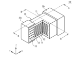
- FIG. 2 is a partial cross-sectional perspective view of a multilayer ceramic capacitor.
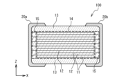
- 4 is a cross-sectional view taken along line AA in FIG. 3.
- 4 is a cross-sectional view taken along line BB in FIG. 3.
- 1 is a diagram illustrating a flow of a method for manufacturing a multilayer ceramic capacitor.
- 4A and 4B are diagrams illustrating an internal electrode forming step.
- 1A to 1C are diagrams illustrating a pressure bonding process.
- 11A and 11B are diagrams illustrating an example of a side margin portion.
- the dielectric ceramic composition according to the first embodiment is a ceramic polycrystalline body containing crystal grains having a perovskite structure represented by the general formula ABO 3. These ceramic polycrystalline bodies contain main phase crystal grains 40 and first crystal grains 41, as exemplified in FIG.
- the main phase crystal particles 40 contain barium titanate having a perovskite structure.
- the first crystal particles 41 contain barium, titanium, and magnesium, and when the elemental ratio of titanium to the barium content is a (hereinafter also referred to as Ti/Ba elemental ratio a) and the elemental ratio of magnesium to the barium content is b (hereinafter also referred to as Mg/Ti elemental ratio b), 5.00 ⁇ a ⁇ 7.00 and 0.50 ⁇ b ⁇ 1.50 are satisfied.
- the area ratio of the main phase crystal grains 40 is 50.0% or more and 99.95% or less, and the area ratio of the first crystal grains 41 is 0.050% or more and 45.0% or less.
- the barium titanate crystal grains having a perovskite structure which are the main component of the main phase crystal grains 40, have a unit lattice as shown in FIG. 2.
- this unit lattice there are A sites located at the vertices of the lattice, O sites located at the face centers of the lattice, and B sites located within an octahedron with the O sites as vertices.
- alkaline earth metals that can take divalent cations such as barium (Ba), strontium (Sr), and calcium (Ca) are located at the A sites, and metal atoms that can take tetravalent cations, such as hafnium (Hf), zirconium (Zr), and titanium (Ti), are located at the B sites.
- the perovskite structure also allows for a composition formula that deviates from the stoichiometric composition. That is, the ratio of the A-site element to the B-site element does not necessarily have to be 1:1, and defects may be generated within a range that allows the perovskite structure to be maintained. Also, defects may be generated in oxygen. For example, when the composition formula is A ⁇ BO 3- ⁇ , a composition in the range of 0.98 ⁇ 1.01 and 0 ⁇ 0.20 is allowed.
- the generation of oxygen defects can reduce resistivity or exhibit ionic conductivity, which can reduce the electrical lifespan or increase dielectric loss when used as a multilayer ceramic capacitor, making it impossible to use in practice.
- at least one of the alkaline earth elements magnesium (Mg), calcium (Ca), strontium (Sr), and barium (Ba) may be included in the main phase crystal particles 40 having a perovskite structure as necessary. This can improve resistivity, increase electrical lifespan, and reduce dielectric loss relative to capacitance.
- the main phase crystal particles 40 may contain at least one of the first transition elements scandium (Sc), titanium (Ti), vanadium (V), chromium (Cr), iron (Fe), cobalt (Co), nickel (Ni), copper (Cu), and zinc (Zn). This can improve resistivity, increase electrical life, and reduce dielectric loss relative to capacitance.
- the main phase crystal grains 40 may also contain at least one of the second transition elements yttrium (Y), zirconium (Zr), niobium (Nb), molybdenum (Mo), ruthenium (Ru), rhodium (Rh), palladium (Pd), and silver (Ag) as necessary. This can improve resistivity, increase electrical life, and reduce dielectric loss relative to capacitance.
- the main phase crystal grains 40 may also contain at least one of the third transition elements lanthanum (La), cerium (Ce), praseodymium (Pr), neodymium (Nd), samarium (Sm), europium (Eu), gadolinium (Gd), terbium (Tb), dysprosium (Dy), holmium (Ho), erbium (Er), thulium (Tm), ytterbium (Yb), lutetium (Lu), hafnium (Hf), tantalum (Ta), tungsten (W), rhenium (Re), osmium (Os), iridium (Ir), platinum (Pt), and gold (Au), as necessary. This can improve resistivity, increase electrical life, and reduce dielectric loss relative to capacitance.
- This can improve resistivity, increase electrical life, and reduce dielectric loss relative to capacitance.
- At least one of the above-mentioned alkaline earth element, first transition metal element, second transition metal element, and third transition metal element as an additive, at least one of the alkaline earth element, first transition metal element, second transition metal element, and third transition metal element can be dissolved from the interface of the main phase crystal grain 40 to the inside in a firing temperature range of 1000° C. to 1400° C. for obtaining the dielectric ceramic composition, thereby generating the core portion 411 and the shell portion 412 in the main phase crystal grain 40.
- the dielectric ceramic composition is preferably added with 0.25 mol or more and 2.5 mol or less of gadolinium in terms of gadolinium oxide (Gd 2 O 3 ) to 100 mol of barium titanate so that the Gd/Ti element ratio j, which is the element ratio of gadolinium to the content of barium, is 0.005 ⁇ j ⁇ 0.05.
- gadolinium oxide it is preferable to add 0.2 mol or more and 2.0 mol or less in terms of magnesium oxide (MgO) to 100 mol of barium titanate so that the Mg/Ti element ratio k, which is the magnesium element ratio to the barium content, is 0.002 ⁇ k ⁇ 0.05.
- the added gadolinium, manganese, and titanium react on the surface of the barium titanate crystal particle, and can be generated as a shell portion in the form of a composite perovskite compound considered to be Gd(Ti,Mg) O3 .
- the dielectric ceramic composition can suppress the movement of oxygen defects in the grain boundaries and inside the shell portion, suppress the decrease in resistivity, and improve the electrical life.
- an acceptor element with a lower valence than titanium such as magnesium, dissolves as a B-site element, suppressing the reduction of titanium during reduction firing and improving the insulation resistance. Therefore, as an example, to ensure high insulation resistance in a multilayer ceramic capacitor, it is necessary to dissolve the acceptor element in the shell portion 412.
- the dielectric ceramic composition according to this embodiment includes, in addition to the main phase crystal particles 40 containing barium titanate having a perovskite structure, first crystal particles 41 that satisfy 5.00 ⁇ Ti/Ba element ratio a ⁇ 7.00 and 0.50 ⁇ Mg/Ba element ratio b ⁇ 1.50.
- first crystal particles 41 that satisfy 5.00 ⁇ Ti/Ba element ratio a ⁇ 7.00 and 0.50 ⁇ Mg/Ba element ratio b ⁇ 1.50.
- the Ti/Ba element ratio a is preferably 5.15 or more, and more preferably 5.40 or more to achieve high insulation resistance.
- the Ti/Ba element ratio a is preferably 6.85 or less, and more preferably 6.60 or less to achieve high insulation resistance.
- the Mg/Ba element ratio b is preferably 0.60 or more, and more preferably 0.75 or more to achieve high insulation resistance.
- the Mg/Ba element ratio b is preferably 1.40 or less, and more preferably 1.25 or less, which allows for high insulation resistance to be achieved.
- the first crystal particles 41 further contain manganese and nickel, and when the element ratio of manganese to the barium content is g (hereinafter also referred to as Mn/Ba element ratio g), and the element ratio of nickel to the barium content is h (hereinafter also referred to as Ni/Ba element ratio h), 0.10 ⁇ g ⁇ 4.00 and 0.10 ⁇ h ⁇ 4.00 are preferably satisfied. This is because the decrease in resistivity of the dielectric ceramic composition can be suppressed.
- the Mn/Ba element ratio g is more preferably 0.50 or more, and is even more preferably 1.00 or more to realize high insulation resistance.
- the Mn/Ba element ratio g is more preferably 3.75 or less, and is even more preferably 3.50 or less to realize high insulation resistance.
- the Ni/Ba element ratio h is preferably 0.50 or more, and is even more preferably 1.00 or more to realize high insulation resistance.
- the Ni/Ba element ratio h is preferably 3.75 or less, and more preferably 3.50 or less, which allows for high insulation resistance to be achieved.
- the first crystal particles 41 may also contain at least one of calcium, scandium, vanadium, chromium, iron, cobalt, nickel, copper, zinc, yttrium, zirconium, niobium, and molybdenum. This is because it is possible to suppress a decrease in the resistivity of the dielectric ceramic composition.
- first crystal particles 41 in the dielectric ceramic composition can be confirmed by the following procedure.
- the surface of the dielectric ceramic composition is exposed.
- methods such as cutting or polishing the element can be used.
- the method of cutting or polishing the element is suitable for observation by SEM.
- a thin slice with a thickness of 100 nm or less can be obtained from the surface of the dielectric ceramic composition having a smoothness that can be judged as a mirror surface using an ion beam or the like.
- the thin slice is suitable for observation by STEM.
- the composition of the first crystal particles 41 is identified using an energy dispersive X-ray spectrometry (EDS) or wavelength dispersive X-ray spectrometry (WDS) attached to a scanning electron microscope (SEM) or scanning transmission electron microscope (STEM), an electron probe microanalyzer (EPMA), and a laser-induced inductively coupled plasma mass spectrometry (LA-ICPMS), etc.
- EDS energy dispersive X-ray spectrometry
- WDS wavelength dispersive X-ray spectrometry
- SEM scanning electron microscope
- STEM scanning transmission electron microscope
- EPMA electron probe microanalyzer
- LA-ICPMS laser-induced inductively coupled plasma mass spectrometry
- EDS measurements they are simply identified by the K-line intensity of titanium and the K-line intensity of magnesium relative to the K-line or L-line of barium. More specifically, from these intensities, corrections are made that take into account the atomic number effect, absorption effect, and fluorescence excitation effect (ZAF corrections), and the ratio of each to the elemental content of barium is calculated, which is the ratio of each element.
- ZAF corrections the ratio of each to the elemental content of barium is calculated, which is the ratio of each element.
- the energy peaks are close to each other, making it difficult to adequately compare element contents. For this reason, it is desirable to obtain barium L ⁇ 2 rays and LIIIab rays with sufficient intensity and without peak overlap during measurement. Specifically, it is desirable for the intensity at the peak to be 10,000 counts or more. At this time, the intensity of the characteristic X-rays from barium can be identified and the element content can be calculated, so even if the barium L ⁇ rays and titanium K ⁇ rays overlap, the intensity of the titanium K ⁇ rays can be identified and the element content can be evaluated with high accuracy.
- the crystal particle can be determined to be the first crystal particle 41.
- the first crystal particle 41 is determined to be a barium titanate composite oxide because the element ratio of titanium and magnesium to barium is larger than that of the main phase crystal particle 40 made of barium titanate that exists around it.
- BSE image Back Scattered Electron Image
- the first crystal particles 41 are characterized by being observed to have a relatively low brightness and appear darker than the main phase crystal particles 40 in high-angle annular dark-field scanning transmission electron microscopy images (HAADF-STEM images).
- the manganese content and nickel content in the first crystal particles 41 are simply quantified using the K-line intensity of manganese and the K-line intensity of nickel relative to the K-line or L-line of barium. More specifically, from these intensities, a correction (ZAF correction) is made that takes into account the atomic number effect, absorption effect, and fluorescence excitation effect, and the ratio of each to the element content of barium is calculated to obtain the ratio of each element. Furthermore, when the particle diameter of the first crystal particles 41 is smaller than the spatial resolution of EDS analysis with an SEM, it is preferable to observe the first crystal particles 41 with a scanning transmission electron microscope (STEM) and identify the composition of the first crystal particles 41 using EDS.
- STEM scanning transmission electron microscope
- the dielectric ceramic composition preferably contains second crystal particles 42 in addition to main phase crystal particles 40 and first crystal particles 41.
- the second crystal particles 42 contain barium, titanium, magnesium, manganese, and nickel, and have an elemental ratio of titanium to the barium content of c (hereinafter also referred to as Ti/Ba elemental ratio c), and an elemental ratio of magnesium to the barium content of d (hereinafter also referred to as Mg/Ba elemental ratio d).
- the element ratio of manganese relative to the barium content is e (hereinafter also referred to as Mn/Ba element ratio e), and the element ratio of nickel relative to the barium content is f (hereinafter also referred to as Ni/Ba element ratio f),
- the Ti/Ba element ratio c is 1.50 ⁇ Ti/Ba element ratio c ⁇ 3.50
- the Mg/Ba element ratio d is 0.03 ⁇ Mg/Ba element ratio d ⁇ 0.30
- the Mn/Ba element ratio e is 0.30
- the Ni/Ba element ratio f is 0.40.
- the area ratio of the main phase crystal grains 40 is 50.0% or more and 99.95% or less
- the area ratio of the first crystal grains 41 is 0.050% or more and 45.0% or less
- the area ratio of the second crystal grains 42 is 0.050% or more and 15.0% or less.
- the second crystal particles 42 are by-produced crystal particles when an additive containing titanium as the main component is used. By intentionally precipitating the second crystal particles 42, the main phase crystal particles 4 and the first crystal particles 41 are obtained, and it is possible to obtain high insulation resistance in a multilayer ceramic capacitor, which requires high reliability.
- the Ti/Ba element ratio c is more preferably 1.70 or more, and more preferably 1.90 or more to achieve high insulation resistance.
- the Ti/Ba element ratio c is more preferably 2.70 or less, and more preferably 2.50 or less to achieve high insulation resistance.
- the Mg/Ba element ratio d is preferably 0.05 or more, and more preferably 0.08 or more to achieve high insulation resistance.
- the Mg/Ba element ratio d is preferably 0.25 or less, and more preferably 0.20 or less to achieve high insulation resistance.
- the Mn/Ba element ratio e is more preferably 0.05 or more, and more preferably 0.08 or more to achieve high insulation resistance.
- the Mn/Ba element ratio e is more preferably 0.25 or less, and more preferably 0.20 or less to achieve high insulation resistance.
- the Ni/Ba element ratio f is preferably 0.05 or more, and more preferably 0.10 or more to achieve high insulation resistance.
- the Ni/Ba element ratio f is preferably 0.35 or less, and more preferably 0.30 or less to achieve high insulation resistance.
- the second crystal particles 42 may further contain at least one of calcium, scandium, vanadium, chromium, iron, cobalt, nickel, copper, zinc, yttrium, zirconium, niobium, and molybdenum. This is because it is possible to suppress a decrease in the resistivity of the dielectric ceramic composition.
- second crystal particles 42 in the dielectric ceramic composition can be confirmed by the following procedure.
- the surface of the dielectric ceramic composition is exposed.
- methods such as cutting or polishing the element can be used.
- a smoothness that can be judged as a mirror surface using diamond paste or the like of 2 microns or less is suitable for observation by SEM.
- a thin slice with a thickness of 100 nm or less can be obtained from the surface of the dielectric ceramic composition having the smoothness that can be judged as a mirror surface using an ion beam or the like.
- the above-mentioned thin slice is suitable for observation by STEM.
- composition of the second crystal particles 42 is identified using an EDS or WDS, EPMA, and LA-ICPMS attached to an SEM or STEM.
- the elements are simply identified by the K-line intensity of titanium, the K-line intensity of magnesium, the K-line intensity of manganese, and the K-line intensity of nickel relative to the K-line or L-line of barium. More specifically, from these intensities, correction (ZAF correction) is performed taking into account the atomic number effect, the absorption effect, and the fluorescence excitation effect, and the ratio of each to the element content of barium is calculated to be the ratio of each element.
- correction may be performed using the proportionality coefficient (K factor) used in the Cliff-Florimer method to obtain the ratio of each element.
- correction may be performed taking into account the absorption effect of the sample to obtain the ratio of each element.
- the absorption effect of the sample can be corrected by determining the thickness and density of the sample.
- the thickness of the sample can be obtained, for example, by acquiring a convergent-beam electron diffraction (CBED) pattern under two-wave excitation conditions and analyzing the rocking curve observed on a diffraction disk.
- the particles from which the CBED pattern is acquired can be the main phase crystal particles 40 or the like.
- the density of the sample can be, for example, 6.02 g/cm 3, which is the density of barium titanate.
- the energy peaks are close to each other, making it difficult to adequately compare element contents. For this reason, it is desirable to obtain barium L ⁇ 2 rays and LIIIab rays with sufficient intensity and without peak overlap during measurement. Specifically, it is desirable for the intensity at the peak to be 10,000 counts or more. At this time, the intensity of the characteristic X-rays from barium can be identified and the element content can be calculated, so even if the barium L ⁇ rays and titanium K ⁇ rays overlap, the intensity of the titanium K ⁇ rays can be identified and the element content can be evaluated with high accuracy.
- the crystal particle can be determined to be the second crystal particle 42.
- the second crystal particle 42 is determined to be a barium titanate composite oxide because the element ratios of titanium, magnesium, manganese, and nickel to barium are larger than those of the main phase crystal particle 40 made of barium titanate present in the periphery, and the element ratios of titanium, magnesium, manganese, and nickel to barium are smaller than those of the first crystal particle 41.
- the second crystal particles 42 are characterized in that, in the observation by a back scattered electron image (BSE image), the second crystal particles 42 are observed to have a relatively low brightness and are darker than the main phase crystal particles 40.
- the second crystal particles 42 are characterized in that, in the observation by a high-angle annular dark-field scanning transmission electron microscopy image (HAADF-STEM image), the second crystal particles 42 are characterized in that, in the observation by a high-angle annular dark-field scanning transmission electron microscopy image (HAADF-STEM image), the second crystal particles 42 are characterized in that, in the observation by a high-angle annular dark-field scanning transmission electron microscopy image (HAADF-STEM image), the second crystal particles 42 are observed to have a relatively low brightness and are darker than the main phase crystal particles 40.
- HAADF-STEM image high-angle annular dark-field scanning transmission electron microscopy image
- HAADF-STEM image high-angle annular dark-field scanning transmission electron microscopy image
- the manganese content and nickel content contained in the second crystal particles 42 are simply quantified using the K-line intensity of manganese and the K-line intensity of nickel relative to the K-line or L-line of barium. More specifically, from these intensities, correction (ZAF correction) is performed taking into account the atomic number effect, the absorption effect, and the fluorescence excitation effect, and the ratio of each to the element content of barium is calculated to obtain the ratio of each element.
- correction may be performed using the proportional coefficient (K factor) used in the Cliff-Flow-Limer method to obtain the ratio of each element.
- correction may be performed taking into account the absorption effect of the sample to obtain the ratio of each element.
- the absorption effect of the sample can be corrected by determining the thickness and density of the sample.
- the thickness of the sample can be obtained, for example, by acquiring a convergent-beam electron diffraction (CBED) pattern under two-wave excitation conditions and analyzing the rocking curve observed on a diffraction disk.
- the particles from which the CBED pattern is acquired can be the main phase crystal particles 40 or the like.
- the density of the sample can be, for example, a value of 6.02 g/ cm3 , which is the density of barium titanate.
- the particle diameter of the second crystal particles 42 is smaller than the spatial resolution of the EDS analysis using an SEM, it is desirable to identify the composition of the second crystal particles 42 using a scanning transmission electron microscope (STEM).
- STEM scanning transmission electron microscope
- the dielectric ceramic composition may also contain third crystal grains 43, voids 44, and the like, which have a different composition or crystal structure from the main phase crystal grains 40, the first crystal grains 41, the second crystal grains 42, and the third crystal grains 43.
- the area ratio of the third crystal grains 43 is 0.050% or more and 15.0% or less.
- the third crystal particles 43 are crystal particles such as silicate (SiO 2 ), enstatite (MgSiO 3 ), barium magnesium silicate (BaMgSiO 4 ), and fresnoite (Ba 2 TiSi 2 O 8 ).
- the dielectric ceramic composition can be sufficiently densified by firing at 1300° C. or less.
- glass particles such as silicate (SiO 2 ), enstatite (MgSiO 3 ), barium magnesium silicate (BaMgSiO 4 ), and fresnoite (Ba 2 TiSi 2 O 8 ) may be included in the dielectric ceramic composition.
- the dielectric ceramic composition may contain secondary compounds derived from added substances or derived from the electrodes, such as geikierite ( MgTiO3 ), manganese nickel oxide ((Mn,Ni)O), and pyrophanite ( MnTiO3 ).
- secondary compounds derived from added substances or derived from the electrodes such as geikierite ( MgTiO3 ), manganese nickel oxide ((Mn,Ni)O), and pyrophanite ( MnTiO3 ).
- the first crystal grains 41 and the second crystal grains 42 are located at the grain boundaries of the main phase crystal grains 40. This is because it is possible to suppress a decrease in the resistivity of the dielectric ceramic composition.
- the first crystal grain 41 and the second crystal grain 42 are preferably located at the grain boundary triple junction of the main phase crystal grain 40. This is because it is possible to suppress a decrease in the resistivity of the dielectric ceramic composition.
- the grain boundary triple junction is the boundary between three crystal grain boundaries.
- the third crystal grains 43 are preferably located at the grain boundaries of the main phase crystal grains 40. This is because it is possible to suppress a decrease in the relative dielectric constant of the dielectric ceramic composition.
- the third crystal grains 43 are preferably located at the grain boundary triple junctions of the main phase crystal grains 40. This is because it is possible to suppress a decrease in the relative dielectric constant of the dielectric ceramic composition.
- the shell portion 412 of the main phase crystal grains 40 contains a rare earth element, because this improves the life of the dielectric ceramic composition.
- the element ratio of titanium to the barium content is greater than 0.940 and less than or equal to 0.980. This is because sufficient first crystal grains 41 and second crystal grains 42 are generated.
- Second Embodiment In the second embodiment, a laminated ceramic capacitor 100 using the dielectric ceramic composition according to the first embodiment will be described.
- FIG. 3 is a partial cross-sectional perspective view of the multilayer ceramic capacitor 100.
- FIG. 4 is a cross-sectional view taken along line A-A in FIG. 3.
- FIG. 5 is a cross-sectional view taken along line B-B in FIG. 3.
- the multilayer ceramic capacitor 100 comprises a laminated chip 10 having a substantially rectangular parallelepiped shape, and external electrodes 20a, 20b provided on either of two opposing end faces of the laminated chip 10. Of the four faces of the laminated chip 10 other than the two end faces, the two faces other than the top and bottom faces in the stacking direction are referred to as side faces.
- the external electrodes 20a, 20b extend on the top, bottom and two side faces in the stacking direction of the laminated chip 10. However, the external electrodes 20a, 20b are spaced apart from each other.
- the laminated chip 10 has a configuration in which dielectric layers 11 containing a dielectric ceramic composition and internal electrode layers 12 containing a base metal material are alternately laminated. The edges of each internal electrode layer 12 are alternately exposed to the end face of the laminated chip 10 on which the external electrode 20a is provided and the end face on which the external electrode 20b is provided. As a result, each internal electrode layer 12 is alternately conductive to the external electrode 20a and the external electrode 20b. As a result, the laminated ceramic capacitor 100 has a configuration in which multiple dielectric layers 11 are laminated via the internal electrode layers 12.
- the internal electrode layer 12 is arranged on the outermost layer in the lamination direction, and the upper and lower surfaces of the laminate are covered by the cover layer 13.
- the cover layer 13 is mainly composed of a ceramic material.
- the material of the cover layer 13 is the same as that of the dielectric layers 11 and the ceramic material.
- the size of the multilayer ceramic capacitor 100 is, for example, 0.25 mm long, 0.125 mm wide, and 0.125 mm high, or 0.4 mm long, 0.2 mm wide, and 0.2 mm high, or 0.6 mm long, 0.3 mm wide, and 0.3 mm high, or 1.0 mm long, 0.5 mm wide, and 0.5 mm high, or 3.2 mm long, 1.6 mm wide, and 1.6 mm high, or 4.5 mm long, 3.2 mm wide, and 2.5 mm high, but is not limited to these sizes.
- the internal electrode layer 12 is mainly composed of base metals such as Ni (nickel), Cu (copper), and Sn (tin).
- Noble metals such as Pt (platinum), Pd (palladium), Ag (silver), and Au (gold), or alloys containing these metals, may also be used as the internal electrode layer 12.
- the region where the internal electrode layer 12 connected to the external electrode 20a and the internal electrode layer 12 connected to the external electrode 20b face each other is a region that generates capacitance in the multilayer ceramic capacitor 100. Therefore, this region that generates capacitance is referred to as the capacitance region 14.
- the capacitance region 14 is a region where adjacent internal electrode layers 12 connected to different external electrodes face each other.
- the region where the internal electrode layers 12 connected to the external electrode 20a face each other without an internal electrode layer 12 connected to the external electrode 20b being interposed therebetween is called the end margin 15.
- the region where the internal electrode layers 12 connected to the external electrode 20b face each other without an internal electrode layer 12 connected to the external electrode 20a being interposed therebetween is also an end margin 15.
- the end margin 15 is the region where the internal electrode layers 12 connected to the same external electrode face each other without an internal electrode layer 12 connected to a different external electrode being interposed therebetween.
- the end margin 15 is a region that does not generate electrical capacitance.
- the side margin 16 is a region that is provided to cover the ends of the multiple internal electrode layers 12 that are laminated in the laminated structure and extend to the two side faces.
- the side margin 16 is also a region that does not generate electrical capacitance.
- the dielectric layer 11 in the capacitance region 14 contains the main phase crystal grains 40 and the first crystal grains 41 illustrated in FIG. 1. This makes it possible to realize high reliability and high insulation resistance.
- 1 is a diagram illustrating a flow of a method for manufacturing the multilayer ceramic capacitor 100.
- a dielectric ceramic composition for forming the dielectric layer 11 is prepared.
- the A-site elements and B-site elements contained in the dielectric layer 11 are usually contained in the dielectric layer 11 in the form of a sintered body of ABO3 particles.
- barium titanate is a compound that has a perovskite structure and belongs to the tetragonal system at around room temperature, and shows a high relative dielectric constant. This barium titanate can generally be synthesized by reacting a titanium raw material such as titanium dioxide with a barium raw material such as barium carbonate.
- a specific additive is added to the barium titanate powder obtained by the above method.
- additives within the range shown in the example of the dielectric ceramic composition according to the first embodiment are used.
- oxides or glasses containing Zr (zirconium), V (vanadium), Cr (chromium), Co (cobalt), Ni (nickel), Li (lithium), B (boron), Na (sodium), and K (potassium) may be used.
- oxides of Sc (scandium), Y (yttrium), La (lanthanum), Ce (cerium), Pr (praseodymium), Nd (neodymium), Pm (promethium), Sm (samarium), Tb (terbium), Dy (dysprosium), Ho (holmium), Er (erbium), Tm (thulium), Y (ytterbium), and Lu (lutetium) may be added as rare earth elements.
- an additive having titanium as a main component in an amount of 0.002 mol or more and 0.06 mol or less in terms of titanium oxide (TiO 2 ) to 1 mol of barium titanate, and add an additive having magnesium as a main component in an amount of 0.002 mol or more and 0.05 mol or less in terms of magnesium oxide (MgO).
- TiO 2 titanium oxide
- MgO magnesium oxide
- the additive having titanium as a main component titanium hydroxide (Ti(OH) 4 ), titanium chloride (TiCl 4 ), titanium carbide (TiC), titanium sulfide (TiS 2 ), etc. may be used in addition to titanium oxide.
- magnesium hydroxide MgOH
- magnesium chloride MgCl 2
- magnesium carbonate MgCO 3
- magnesium sulfide MgS
- an additive whose main component is titanium which is 0.002 mol or more and 0.08 mol or less in terms of titanium oxide (TiO 2 )
- an additive whose main component is magnesium which is 0.002 mol or more and 0.05 mol or less in terms of magnesium oxide (MgO)
- an additive whose main component is manganese which is 0.002 mol or more and 0.05 mol or less in terms of manganese carbonate (MnCO 3 ), to 1 mol of barium titanate.
- titanium hydroxide (Ti(OH) 4 ), titanium chloride (TiCl 4 ), titanium carbide (TiC), titanium sulfide (TiS 2 ), etc. may be used in addition to titanium oxide.
- titanium hydroxide (MgOH), magnesium chloride ( MgCl2 ), magnesium carbonate ( MgCO3 ), magnesium sulfide (MgS), etc. may be used in addition to magnesium oxide.
- manganese manganese monoxide (MnO), manganese trioxide ( Mn3O4 ), manganese dioxide ( MnO2 ), etc. may be used in addition to manganese carbonate .
- a compound containing an additive compound is wet mixed with barium titanate powder, and then dried and pulverized to prepare a ceramic material in which barium titanate powder and the additive compound are mixed.
- the ceramic material obtained as described above may be pulverized as necessary to adjust the particle size, or may be combined with a classification process to adjust the particle size. Through the above steps, a dielectric ceramic composition is obtained.
- a binder such as polyvinyl butyral (PVB) resin, an organic solvent such as ethanol or toluene, and a plasticizer are added to the obtained dielectric ceramic composition and wet mixed.
- the obtained slurry is used to coat a ceramic green sheet 51 on a substrate by, for example, a die coater method or a doctor blade method, and then dried.
- the substrate is, for example, a polyethylene terephthalate (PET) film.
- PET polyethylene terephthalate
- a metal conductive paste containing an organic binder for forming internal electrodes is printed on the surface of the ceramic green sheet 51 by screen printing, gravure printing, or the like to form electrodes having different polarities.
- the internal electrode patterns 52 are arranged so that they are alternately drawn out to a pair of external electrodes.
- Ceramic particles are added to the metal conductive paste as a co-material.
- the main component of the ceramic particles is not particularly limited, but may be the same as that of the dielectric layer. It is preferable that the main component ceramic is the same as that of No. 11.
- barium titanate having an average particle size of 50 nm or less may be uniformly dispersed.
- a binder such as an ethyl cellulose-based binder and an organic solvent such as a terpineol-based binder are added to the dielectric ceramic composition obtained in the raw powder preparation process, and the mixture is kneaded in a roll mill to obtain a dielectric pattern paste for the reverse pattern layer.
- the dielectric pattern paste is printed on the peripheral area of a ceramic green sheet 51 where the internal electrode pattern 52 is not printed, thereby arranging the dielectric pattern 53 and filling in the step with the internal electrode pattern 52.
- the ceramic green sheet 51 on which the internal electrode pattern 52 and the dielectric pattern 53 are printed is referred to as a stacking unit.
- the stacking units are stacked so that the internal electrode layers 12 and the dielectric layers 11 are staggered, and so that the edges of the internal electrode layers 12 are alternately exposed on both longitudinal end faces of the dielectric layers 11 and alternately drawn out to a pair of external electrodes 20a, 20b of opposite polarity.
- the number of stacked layers of the internal electrode pattern 52 is 100 to 1000.
- a predetermined number of cover sheets 54 are laminated on the top and bottom of the laminate in which the lamination units are stacked, and then thermocompression bonded.
- the ceramic material of the cover sheets 54 the above-mentioned dielectric ceramic composition can be used. Then, the laminate is cut to a predetermined chip size (e.g., 1.0 mm x 0.5 mm).
- the ceramic laminate thus obtained is subjected to a binder removal process in an N2 atmosphere, an air atmosphere, or the like, and then a metal paste that will become the base layer of the external electrodes 20a, 20b is applied by a dipping method, and the laminate is fired at 1100 to 1300°C for 10 minutes to 2 hours in a reducing atmosphere with an oxygen partial pressure of 10-12 to 10-9 atm. In this manner, the multilayer ceramic capacitor 100 is obtained.
- the temperature is rapidly increased.
- the temperature increase rate in the firing process is, for example, 6000°C/h. This shortens the actual firing time, making it possible to obtain higher mass productivity.
- the resultant is annealed at 900 to 1150° C. for 30 minutes to 2 hours in a reducing atmosphere with an oxygen partial pressure of 10 ⁇ 12 to 10 ⁇ 9 atm, and then slowly cooled.
- the cooling rate is, for example, 200° C./h.
- the main phase crystal grains 40 illustrated in FIG. 1 can be formed in at least a portion of the dielectric layer 11 in the capacitance region 14, and the first crystal grains 41 can also be formed.
- a re-oxidation treatment may be performed at 600° C. to 1000° C. in a N 2 gas atmosphere.
- the underlayers of the external electrodes 20a, 20b are coated with a metal such as Cu, Ni, Sn, etc. by plating.
- a metal such as Cu, Ni, Sn, etc.
- the main phase crystal grains 40 illustrated in FIG. 1 can be formed in at least a portion of the dielectric layer 11 in the capacitance region 14, and the first crystal grains 41 can also be formed. This makes it possible to achieve high reliability and high insulation resistance.
- the DC resistivity ⁇ ( ⁇ cm) of multilayer ceramic capacitors is measured using the following method.
- the DC current I (nA) is measured for the multilayer ceramic capacitor 100 that has undergone the firing process, annealing process, reoxidation process, and plating process.
- the capacitance region 14 of the multilayer ceramic capacitor 100 is exposed by cutting or polishing the cross section of line A-A and the cross section of line B-B shown in Figures 4 and 5, and the effective area of the internal electrode layer 12 is calculated in a state where a smoothness that can be judged as a mirror surface is obtained using a diamond paste of 2 microns or less.
- the thickness of each dielectric layer 11 is also measured, and the average thickness t is calculated.
- a multilayer ceramic capacitor has been described as an example of a multilayer ceramic electronic component, but the present invention is not limited to this.
- other multilayer ceramic electronic components such as varistors and thermistors may also be used.
- Example 1 A barium titanate powder having an average particle size of 150 nm was prepared, and 0.75 mol of Gd2O3 , 2.0 mol of TiO2 , 1.5 mol of MnCO3 , 1.0 mol of SiO2 , and 0.5 mol of MgO were added to 100 mol of the barium titanate powder to obtain a dielectric ceramic composition.
- the Ba/Ti element ratio was 0.980.
- the dielectric ceramic composition was mixed with ethanol, toluene, and PVB (polyvinyl butyral) resin to prepare a dielectric slurry.
- This slurry was formed into a ceramic green sheet using a die coater and dried.
- a metal conductive paste containing the main component metal of the internal electrode layer 12, a common material, a binder (ethyl cellulose), a solvent, and other auxiliary agents as necessary was prepared using a planetary ball mill and screen printed on the ceramic green sheet. Eleven laminate units with the metal conductive paste printed on the ceramic green sheet were stacked, and cover sheets were laminated on the top and bottom of each. A laminate was then obtained by thermocompression bonding and cut into a specified shape.
- a metal conductive paste containing a metal filler mainly composed of Ni, a common material, a binder, a solvent, etc. was applied as a base layer from both end faces to each side of the laminate and dried. Then, the metal conductive paste for the base layer was fired simultaneously with the laminate at 1300°C in a reducing atmosphere to obtain a sintered body. The heating rate was 6000°C/h. The dimensions of the resulting sintered body were length 0.6 mm, width 0.3 mm, and height 0.3 mm. Then, annealing treatment was performed at 900 to 1150°C for 1 hour. Then, reoxidation treatment was performed at 950°C.
- the average thickness of the dielectric layer 11 was 2.0 ⁇ m.
- Example 2 In Example 2, 0.75 mol of Gd2O3 , 4.0 mol of TiO2 , 1.5 mol of MnCO3, 1.0 mol of SiO2 , and 0.5 mol of MgO were added to 100 mol of barium titanate powder to obtain a dielectric ceramic composition.
- the Ba/Ti element ratio was 0.962.
- the firing temperature was 1250°C.
- the annealing time was 1 hour.
- the other conditions were the same as those of Example 1.
- Example 3 In Example 3, 0.75 mol of Gd2O3 , 4.0 mol of TiO2 , 1.5 mol of MnCO3, 1.0 mol of SiO2 , and 0.5 mol of MgO were added to 100 mol of barium titanate powder to obtain a dielectric ceramic composition.
- the Ba/Ti element ratio was 0.962.
- the firing temperature was 1250°C.
- the annealing time was 0.5 hours.
- the other conditions were the same as those of Example 1.
- Example 4 In Example 4, 0.75 mol of Gd2O3 , 4.0 mol of TiO2 , 1.5 mol of MnCO3 , 1.0 mol of SiO2, and 0.5 mol of MgO were added to 100 mol of barium titanate powder to obtain a dielectric ceramic composition.
- the Ba/Ti element ratio was 0.962.
- the firing temperature was 1250°C.
- the annealing time was 2 hours.
- the other conditions were the same as those of Example 1.
- Example 5 In Example 5, 0.75 mol of Gd2O3 , 6.0 mol of TiO2 , 1.5 mol of MnCO3, 1.0 mol of SiO2 , and 0.5 mol of MgO were added to 100 mol of barium titanate powder to obtain a dielectric ceramic composition.
- the Ba/Ti element ratio was 0.943.
- the firing temperature was 1200°C.
- the annealing time was 1 hour.
- the other conditions were the same as those of Example 1.
- Example 6 In Example 6, 0.75 mol of Gd2O3 , 4.0 mol of TiO2 , 1.5 mol of MnCO3, 1.0 mol of SiO2 , and 0.2 mol of MgO were added to 100 mol of barium titanate powder to obtain a dielectric ceramic composition.
- the Ba/Ti element ratio was 0.962.
- the firing temperature was 1280°C.
- the annealing time was 1 hour.
- the other conditions were the same as those of Example 1.
- Example 7 In Example 7, 0.75 mol of Gd2O3 , 4.0 mol of TiO2 , 1.5 mol of MnCO3, 1.0 mol of SiO2 , and 1.0 mol of MgO were added to 100 mol of barium titanate powder to obtain a dielectric ceramic composition.
- the Ba/Ti element ratio was 0.962.
- the firing temperature was 1250°C.
- the annealing time was 1 hour.
- the other conditions were the same as those of Example 1.
- Example 8 In Example 8, 0.75 mol of Gd2O3 , 4.0 mol of TiO2 , 1.5 mol of MnCO3, 1.0 mol of SiO2 , and 2.0 mol of MgO were added to 100 mol of barium titanate powder to obtain a dielectric ceramic composition.
- the Ba/Ti element ratio was 0.962.
- the firing temperature was 1250°C.
- the annealing time was 1 hour.
- the other conditions were the same as those of Example 1.
- Example 9 In Example 9, 0.75 mol of Gd2O3 , 4.0 mol of TiO2 , 1.5 mol of MnCO3, 0.2 mol of SiO2, and 0.5 mol of MgO were added to 100 mol of barium titanate powder to obtain a dielectric ceramic composition.
- the Ba/Ti element ratio was 0.962.
- the firing temperature was 1300°C.
- the annealing time was 1 hour.
- the other conditions were the same as those of Example 1.
- Example 10 In Example 10, 0.75 mol of Gd2O3 , 4.0 mol of TiO2 , 1.5 mol of MnCO3 , 0.5 mol of SiO2 , and 0.5 mol of MgO were added to 100 mol of barium titanate powder to obtain a dielectric ceramic composition.
- the Ba/Ti element ratio was 0.962.
- the firing temperature was 1300°C.
- the annealing time was 1 hour.
- the other conditions were the same as those of Example 1.
- Example 11 In Example 11, 0.75 mol of Gd2O3 , 4.0 mol of TiO2 , 1.5 mol of MnCO3 , 2.0 mol of SiO2 , and 0.5 mol of MgO were added to 100 mol of barium titanate powder to obtain a dielectric ceramic composition.
- the Ba/Ti element ratio was 0.962.
- the firing temperature was 1200°C.
- the annealing time was 1 hour.
- the other conditions were the same as those of Example 1.
- Example 12 In Example 12, 0.75 mol of Gd2O3 , 4.0 mol of TiO2 , 5.0 mol of MnCO3, 0.5 mol of SiO2 , and 0.5 mol of MgO were added to 100 mol of barium titanate powder to obtain a dielectric ceramic composition.
- the Ba/Ti element ratio was 0.962.
- the firing temperature was 1300°C.
- the annealing time was 0.5 hours.
- the other conditions were the same as those of Example 1.
- Example 13 In Example 13, 0.75 mol of Gd2O3 , 4.0 mol of TiO2 , 0.2 mol of MnCO3, 0.5 mol of SiO2 , and 0.5 mol of MgO were added to 100 mol of barium titanate powder to obtain a dielectric ceramic composition.
- the Ba/Ti element ratio was 0.962.
- the firing temperature was 1300°C.
- the annealing time was 2 hours.
- the other conditions were the same as those of Example 1.
- Comparative Example 1 In Comparative Example 1, 0.75 mol of Gd2O3 , 1.0 mol of TiO2 , 1.5 mol of MnCO3 , 1.0 mol of SiO2 , and 0.5 mol of MgO were added to 100 mol of barium titanate powder to obtain a dielectric ceramic composition.
- the Ba/Ti element ratio was 0.990.
- the firing temperature was 1320°C.
- the annealing time was 2 hours. The other conditions were the same as those of Example 1.
- Comparative Example 2 In Comparative Example 2, 0.75 mol of Gd2O3 , 8.0 mol of TiO2 , 1.5 mol of MnCO3 , 1.0 mol of SiO2 , and 0.5 mol of MgO were added to 100 mol of barium titanate powder to obtain a dielectric ceramic composition.
- the Ba/Ti element ratio was 0.926.
- the firing temperature was 1160°C.
- the annealing time was 1 hour.
- the other conditions were the same as those of Example 1.
- Comparative Example 3 In Comparative Example 3, 0.75 mol of Gd2O3 , 4.0 mol of TiO2 , 1.5 mol of MnCO3 , 1.0 mol of SiO2 , and 0.05 mol of MgO were added to 100 mol of barium titanate powder to obtain a dielectric ceramic composition.
- the Ba/Ti element ratio was 0.962.
- the firing temperature was 1300°C.
- the annealing time was 1 hour.
- the other conditions were the same as those of Example 1.
- Comparative Example 4 In Comparative Example 4, 0.75 mol of Gd2O3 , 4.0 mol of TiO2 , 1.5 mol of MnCO3 , 1.0 mol of SiO2 , and 5.0 mol of MgO were added to 100 mol of barium titanate powder to obtain a dielectric ceramic composition.
- the Ba/Ti element ratio was 0.962.
- the firing temperature was 1200°C.
- the annealing time was 1 hour.
- the other conditions were the same as those of Example 1.
- Comparative Example 5 In Comparative Example 5, 0.75 mol of Gd2O3 , 4.0 mol of TiO2 , 1.5 mol of MnCO3 , 1.0 mol of SiO2 , and 0.5 mol of MgO were added to 100 mol of barium titanate powder to obtain a dielectric ceramic composition.
- the Ba/Ti element ratio was 0.962.
- the firing temperature was 1250°C.
- the annealing time was 0 hours. In other words, no annealing treatment was performed. The other conditions were the same as those of Example 1.
- the direct current I was measured at 150°C when 60V was applied for 30 seconds using an insulation resistance meter for each of the multilayer ceramic capacitors of Examples 1 to 13 and Comparative Examples 1 to 5, and the resistivity ⁇ was calculated.
- the presence or absence of first crystal particles in the dielectric layer that satisfied 5.00 ⁇ Ti/Ba element ratio a ⁇ 7.00 and 0.50 ⁇ Mg/Ba element ratio b ⁇ 1.50 was confirmed.
- the Ti/Ba element ratio a, Mg/Ba element ratio b, Mn/Ba element ratio g, and Ni/Ba element ratio h in the first crystal particles were measured.
- Example 1 first crystal particles were confirmed.
- the Ti/Ba element ratio a was 5.32
- the Mg/Ba element ratio b was 1.00
- the Mn/Ba element ratio g was 2.28
- the Ni/Ba element ratio h was 1.76.
- second crystal particles were confirmed.
- the Ti/Ba element ratio c was 1.62
- the Mg/Ba element ratio d was 0.14
- the Mn/Ba element ratio e was 0.14
- the Ni/Ba element ratio f was 0.18.
- the resistivity ⁇ was 2.9 ⁇ 10 11 ⁇ cm.
- Example 2 first crystal particles were confirmed.
- the Ti/Ba element ratio a was 5.60
- the Mg/Ba element ratio b was 1.11
- the Mn/Ba element ratio g was 2.85
- the Ni/Ba element ratio h was 2.02.
- second crystal particles were confirmed.
- the Ti/Ba element ratio c was 2.16
- the Mg/Ba element ratio d was 0.13
- the Mn/Ba element ratio e was 0.12
- the Ni/Ba element ratio f was 0.20.
- the resistivity ⁇ was 9.5 ⁇ 10 11 ⁇ cm.
- Example 3 first crystal particles were confirmed.
- the Ti/Ba element ratio a was 5.66
- the Mg/Ba element ratio b was 1.14
- the Mn/Ba element ratio g was 3.42
- the Ni/Ba element ratio h was 1.01.
- second crystal particles were confirmed.
- the Ti/Ba element ratio c was 2.31
- the Mg/Ba element ratio d was 0.12
- the Mn/Ba element ratio e was 0.03
- the Ni/Ba element ratio f was 0.37.
- the resistivity ⁇ was 2.1 ⁇ 10 11 ⁇ cm.
- Example 4 first crystal particles were confirmed.
- the Ti/Ba element ratio a was 5.71
- the Mg/Ba element ratio b was 1.10
- the Mn/Ba element ratio g was 1.71
- the Ni/Ba element ratio h was 3.03.
- no second crystal particles were confirmed.
- the resistivity ⁇ was 4.1 ⁇ 10 10 ⁇ cm.
- Example 5 first crystal particles were confirmed.
- the Ti/Ba element ratio a was 6.85
- the Mg/Ba element ratio b was 1.08
- the Mn/Ba element ratio g was 0.15
- the Ni/Ba element ratio h was 2.10.
- second crystal particles were confirmed.
- the Ti/Ba element ratio c was 3.23
- the Mg/Ba element ratio d was 0.11
- the Mn/Ba element ratio e was 0.12
- the Ni/Ba element ratio f was 0.19.
- the resistivity ⁇ was 1.5 ⁇ 10 11 ⁇ cm.
- Example 6 first crystal particles were confirmed.
- the Ti/Ba element ratio a was 5.82
- the Mg/Ba element ratio b was 0.54
- the Mn/Ba element ratio g was 2.74
- the Ni/Ba element ratio h was 2.04.
- second crystal particles were confirmed.
- the Ti/Ba element ratio c was 2.20
- the Mg/Ba element ratio d was 0.03
- the Mn/Ba element ratio e was 0.12
- the Ni/Ba element ratio f was 0.16.
- the resistivity ⁇ was 2.0 ⁇ 10 11 ⁇ cm.
- Example 7 first crystal particles were confirmed.
- the Ti/Ba element ratio a was 5.71
- the Mg/Ba element ratio b was 1.21
- the Mn/Ba element ratio g was 2.72
- the Ni/Ba element ratio h was 2.02.
- second crystal particles were confirmed.
- the Ti/Ba element ratio c was 2.09
- the Mg/Ba element ratio d was 0.16
- the Mn/Ba element ratio e was 0.11
- the Ni/Ba element ratio f was 0.24.
- the resistivity ⁇ was 6.6 ⁇ 10 11 ⁇ cm.
- Example 8 first crystal particles were confirmed.
- the Ti/Ba element ratio a was 5.60
- the Mg/Ba element ratio b was 1.44
- the Mn/Ba element ratio g was 2.91
- the Ni/Ba element ratio h was 1.94.
- second crystal particles were confirmed.
- the Ti/Ba element ratio c was 2.03
- the Mg/Ba element ratio d was 0.29
- the Mn/Ba element ratio e was 0.11
- the Ni/Ba element ratio f was 0.24.
- the resistivity ⁇ was 2.9 ⁇ 10 11 ⁇ cm.
- Example 9 first crystal particles were confirmed.
- the Ti/Ba element ratio a was 5.15
- the Mg/Ba element ratio b was 0.78
- the Mn/Ba element ratio g was 2.88
- the Ni/Ba element ratio h was 1.96.
- second crystal particles were confirmed.
- the Ti/Ba element ratio c was 2.18
- the Mg/Ba element ratio d was 0.12
- the Mn/Ba element ratio e was 0.12
- the Ni/Ba element ratio f was 0.22.
- the resistivity ⁇ was 5.1 ⁇ 10 11 ⁇ cm.
- Example 10 first crystal particles were confirmed.
- the Ti/Ba element ratio a was 5.26
- the Mg/Ba element ratio b was 0.92
- the Mn/Ba element ratio g was 2.89
- the Ni/Ba element ratio h was 2.00.
- second crystal particles were confirmed.
- the Ti/Ba element ratio c was 2.24
- the Mg/Ba element ratio d was 0.12
- the Mn/Ba element ratio e was 0.12
- the Ni/Ba element ratio f was 0.22.
- the resistivity ⁇ was 4.9 ⁇ 10 11 ⁇ cm.
- Example 11 first crystal particles were confirmed.
- the Ti/Ba element ratio a was 6.72
- the Mg/Ba element ratio b was 1.33
- the Mn/Ba element ratio g was 1.91
- the Ni/Ba element ratio h was 1.98.
- second crystal particles were confirmed.
- the Ti/Ba element ratio c was 2.22
- the Mg/Ba element ratio d was 0.12
- the Mn/Ba element ratio e was 0.12
- the Ni/Ba element ratio f was 0.22.
- the resistivity ⁇ was 3.9 ⁇ 10 11 ⁇ cm.
- Example 12 first crystal particles were confirmed.
- the Ti/Ba element ratio a was 5.38
- the Mg/Ba element ratio b was 0.92
- the Mn/Ba element ratio g was 4.13
- the Ni/Ba element ratio h was 0.07.
- second crystal particles were confirmed.
- the Ti/Ba element ratio c was 2.76
- the Mg/Ba element ratio d was 0.12
- the Mn/Ba element ratio e was 0.02
- the Ni/Ba element ratio f was 0.32.
- the resistivity ⁇ was 2.3 ⁇ 10 10 ⁇ cm.
- Example 13 first crystal particles were confirmed.
- the Ti/Ba element ratio a was 5.43
- the Mg/Ba element ratio b was 0.97
- the Mn/Ba element ratio g was 0.05
- the Ni/Ba element ratio h was 4.12.
- second crystal particles were confirmed.
- the Ti/Ba element ratio c was 1.83
- the Mg/Ba element ratio d was 0.13
- the Mn/Ba element ratio e was 0.32
- the Ni/Ba element ratio f was 0.05.
- the resistivity ⁇ was 2.4 ⁇ 10 10 ⁇ cm.
- the first crystal particles were not observed, but the second crystal particles were observed.
- the Ti/Ba element ratio c was 3.05
- the Mg/Ba element ratio d was 0.11
- the Mn/Ba element ratio e was 0.11
- the Ni/Ba element ratio f was 0.18.
- the resistivity ⁇ was 1.3 ⁇ 10 9 ⁇ cm.
- the first crystal particles were not observed, but the second crystal particles were observed.
- the Ti/Ba element ratio c was 2.37
- the Mg/Ba element ratio d was 0.00
- the Mn/Ba element ratio e was 0.35
- the Ni/Ba element ratio f was 0.38.
- the resistivity ⁇ was 5.8 ⁇ 10 9 ⁇ cm.
- the first crystal particles were not observed, but the second crystal particles were observed.
- the Ti/Ba element ratio c was 2.09
- the Mg/Ba element ratio d was 0.31
- the Mn/Ba element ratio e was 0.11
- the Ni/Ba element ratio f was 0.22.
- the resistivity ⁇ was 1.8 ⁇ 10 9 ⁇ cm.
- the first crystal particles were not observed, but the second crystal particles were observed.
- the Ti/Ba element ratio c was 2.16
- the Mg/Ba element ratio d was 0.13
- the Mn/Ba element ratio e was 0.12
- the Ni/Ba element ratio f was 0.20.
- the resistivity ⁇ was 8.0 ⁇ 10 9 ⁇ cm.
- Examples 1 to 3, 5 to 11 The resistivity of Examples 1 to 3, 5 to 11 was higher than that of Examples 4, 12, and 13. This is thought to be because, in Examples 1 to 3, 5 to 11, second crystal particles were confirmed in addition to the first crystal particles, and the second crystal particles satisfied the following conditions: 1.50 ⁇ Ti/Ba element ratio c ⁇ 3.50, 0.03 ⁇ Mg/Ba element ratio d ⁇ 0.30, 0.03 ⁇ Mn/Ba element ratio e ⁇ 0.30, and 0.03 ⁇ Ni/Ba element ratio f ⁇ 0.40.
- composition evaluation of the main phase crystal particles contained in the dielectric layer using EDS confirmed that the main phase crystal particles had a core-shell structure.
Landscapes
- Engineering & Computer Science (AREA)
- Power Engineering (AREA)
- Chemical & Material Sciences (AREA)
- Ceramic Engineering (AREA)
- Manufacturing & Machinery (AREA)
- Microelectronics & Electronic Packaging (AREA)
- Materials Engineering (AREA)
- Inorganic Chemistry (AREA)
- Structural Engineering (AREA)
- Organic Chemistry (AREA)
- Inorganic Insulating Materials (AREA)
- Compositions Of Oxide Ceramics (AREA)
- Ceramic Capacitors (AREA)
Abstract
Description
第1実施形態に係る誘電体磁器組成物は、一般式ABO3で表されるペロブスカイト構造を有する結晶粒子を含むセラミックス多結晶体である。これらのセラミックス多結晶体は、図1で例示するように、主相結晶粒子40を含むとともに、第1結晶粒子41を含む。
また、第1結晶粒子41の粒子径がSEMでのEDS分析における空間分解能よりも小さい場合、走査型透過電子顕微鏡(STEM: Scanning Transmission Electron Microscope) によって、観察し、第1結晶粒子41における組成を、EDSを用いて同定することが望ましい。
第2実施形態においては、第1実施形態に係る誘電体磁器組成物を用いた積層セラミックコンデンサ100について説明する。
は、積層セラミックコンデンサ100の製造方法のフローを例示する図である。
まず、誘電体層11を形成するための誘電体磁器組成物を用意する。誘電体層11に含まれるAサイト元素およびBサイト元素は、通常はABO3の粒子の焼結体の形で誘電体層11に含まれる。例えば、チタン酸バリウムは、ペロブスカイト構造を有する室温付近において正方晶系に属する化合物であって、高い比誘電率を示す。このチタン酸バリウムは、一般的に、二酸化チタンなどのチタン原料と炭酸バリウムなどのバリウム原料とを反応させて合成することができる。誘電体層11の主成分となるチタン酸バリウムの合成方法としては、従来種々の方法が知られており、例えば固相法、ゾル-ゲル法、水熱法等が知られている。本実施形態においては、これらのいずれも採用することができる。
次に、得られた誘電体磁器組成物に、ポリビニルブチラール(PVB)樹脂等のバインダと、エタノール、トルエン等の有機溶剤と、可塑剤とを加えて湿式混合する。得られたスラリを使用して、例えばダイコータ法やドクターブレード法により、基材上にセラミックグリーンシート51を塗工して乾燥させる。基材は、例えば、ポリエチレンテレフタレート(PET)フィルムである。塗工工程を例示する図は省略した。
次に、図7(a)で例示するように、セラミックグリーンシート51の表面に、有機バインダを含む内部電極形成用の金属導電ペーストをスクリーン印刷、グラビア印刷等により印刷することで、極性の異なる一対の外部電極に交互に引き出される内部電極パターン52を配置する。金属導電ペーストには、共材としてセラミック粒子を添加する。セラミック粒子の主成分は、特に限定するものではないが、誘電体層11の主成分セラミックと同じであることが好ましい。例えば、平均粒子径が50nm以下のチタン酸バリウムを均一に分散させてもよい。
図8で例示するように、積層単位が積層された積層体の上下にカバーシート54を所定数(例えば2~10層)だけ積層して熱圧着する。カバーシート54のセラミック材料として、一例としては上述した誘電体磁器組成物を用いることができる。その後、所定チップ寸法(例えば1.0mm×0.5mm)にカットする。
このようにして得られたセラミック積層体を、N2雰囲気、大気雰囲気、等で脱バインダ処理した後に外部電極20a,20bの下地層となる金属ペーストをディップ法で塗布し、酸素分圧10-12~10-9atmの還元雰囲気中で1100~1300℃で10分~2時間焼成する。このようにして、積層セラミックコンデンサ100が得られる。なお、焼成工程においては、急速昇温を行う。焼成工程における昇温速度は、例えば、6000℃/hである。これにより、焼成における実質的な時間を短縮し、より高い量産性を得ることが可能となる。
その後、酸素分圧10-12~10-9atmの還元雰囲気中で900~1150℃で30分~2時間アニールし、徐冷する。冷却速度は例えば、200℃/hという速度で冷却を行う。このようにして、容量領域14の誘電体層11の少なくとも一部に、図1で例示した主相結晶粒子40を形成することができるとともに、第1結晶粒子41を形成することができる。
その後、N2ガス雰囲気中で600℃~1000℃で再酸化処理を行ってもよい。
その後、外部電極20a,20bの下地層上に、めっき処理により、Cu,Ni,Sn等の金属コーティングを行う。以上の工程により、積層セラミックコンデンサ100が完成する。
平均粒径150nmのチタン酸バリウム粉末を用意し、チタン酸バリウム粉末100molに対して、Gd2O3を0.75mol添加し、TiO2を2.0mol添加し、MnCO3を1.5mol添加し、SiO2を1.0mol添加し、MgOを0.5mol添加し、誘電体磁器組成物を得た。Ba/Ti元素比率は、0.980とした。
実施例2では、チタン酸バリウム粉末100molに対して、Gd2O3を0.75mol添加し、TiO2を4.0mol添加し、MnCO3を1.5mol添加し、SiO2を1.0mol添加し、MgOを0.5mol添加し、誘電体磁器組成物を得た。Ba/Ti元素比率は、0.962とした。焼成温度を1250℃とした。アニール時間を1時間とした。その他の条件は、実施例1と同じとした。
実施例3では、チタン酸バリウム粉末100molに対して、Gd2O3を0.75mol添加し、TiO2を4.0mol添加し、MnCO3を1.5mol添加し、SiO2を1.0mol添加し、MgOを0.5mol添加し、誘電体磁器組成物を得た。Ba/Ti元素比率は、0.962とした。焼成温度を1250℃とした。アニール時間を0.5時間とした。その他の条件は、実施例1と同じとした。
実施例4では、チタン酸バリウム粉末100molに対して、Gd2O3を0.75mol添加し、TiO2を4.0mol添加し、MnCO3を1.5mol添加し、SiO2を1.0mol添加し、MgOを0.5mol添加し、誘電体磁器組成物を得た。Ba/Ti元素比率は、0.962とした。焼成温度を1250℃とした。アニール時間を2時間とした。その他の条件は、実施例1と同じとした。
実施例5では、チタン酸バリウム粉末100molに対して、Gd2O3を0.75mol添加し、TiO2を6.0mol添加し、MnCO3を1.5mol添加し、SiO2を1.0mol添加し、MgOを0.5mol添加し、誘電体磁器組成物を得た。Ba/Ti元素比率は、0.943とした。焼成温度を1200℃とした。アニール時間を1時間とした。その他の条件は、実施例1と同じとした。
実施例6では、チタン酸バリウム粉末100molに対して、Gd2O3を0.75mol添加し、TiO2を4.0mol添加し、MnCO3を1.5mol添加し、SiO2を1.0mol添加し、MgOを0.2mol添加し、誘電体磁器組成物を得た。Ba/Ti元素比率は、0.962とした。焼成温度を1280℃とした。アニール時間を1時間とした。その他の条件は、実施例1と同じとした。
実施例7では、チタン酸バリウム粉末100molに対して、Gd2O3を0.75mol添加し、TiO2を4.0mol添加し、MnCO3を1.5mol添加し、SiO2を1.0mol添加し、MgOを1.0mol添加し、誘電体磁器組成物を得た。Ba/Ti元素比率は、0.962とした。焼成温度を1250℃とした。アニール時間を1時間とした。その他の条件は、実施例1と同じとした。
実施例8では、チタン酸バリウム粉末100molに対して、Gd2O3を0.75mol添加し、TiO2を4.0mol添加し、MnCO3を1.5mol添加し、SiO2を1.0mol添加し、MgOを2.0mol添加し、誘電体磁器組成物を得た。Ba/Ti元素比率は、0.962とした。焼成温度を1250℃とした。アニール時間を1時間とした。その他の条件は、実施例1と同じとした。
実施例9では、チタン酸バリウム粉末100molに対して、Gd2O3を0.75mol添加し、TiO2を4.0mol添加し、MnCO3を1.5mol添加し、SiO2を0.2mol添加し、MgOを0.5mol添加し、誘電体磁器組成物を得た。Ba/Ti元素比率は、0.962とした。焼成温度を1300℃とした。アニール時間を1時間とした。その他の条件は、実施例1と同じとした。
実施例10では、チタン酸バリウム粉末100molに対して、Gd2O3を0.75mol添加し、TiO2を4.0mol添加し、MnCO3を1.5mol添加し、SiO2を0.5mol添加し、MgOを0.5mol添加し、誘電体磁器組成物を得た。Ba/Ti元素比率は、0.962とした。焼成温度を1300℃とした。アニール時間を1時間とした。その他の条件は、実施例1と同じとした。
実施例11では、チタン酸バリウム粉末100molに対して、Gd2O3を0.75mol添加し、TiO2を4.0mol添加し、MnCO3を1.5mol添加し、SiO2を2.0mol添加し、MgOを0.5mol添加し、誘電体磁器組成物を得た。Ba/Ti元素比率は、0.962とした。焼成温度を1200℃とした。アニール時間を1時間とした。その他の条件は、実施例1と同じとした。
実施例12では、チタン酸バリウム粉末100molに対して、Gd2O3を0.75mol添加し、TiO2を4.0mol添加し、MnCO3を5.0mol添加し、SiO2を0.5mol添加し、MgOを0.5mol添加し、誘電体磁器組成物を得た。Ba/Ti元素比率は、0.962とした。焼成温度を1300℃とした。アニール時間を0.5時間とした。その他の条件は、実施例1と同じとした。
実施例13では、チタン酸バリウム粉末100molに対して、Gd2O3を0.75mol添加し、TiO2を4.0mol添加し、MnCO3を0.2mol添加し、SiO2を0.5mol添加し、MgOを0.5mol添加し、誘電体磁器組成物を得た。Ba/Ti元素比率は、0.962とした。焼成温度を1300℃とした。アニール時間を2時間とした。その他の条件は、実施例1と同じとした。
比較例1では、チタン酸バリウム粉末100molに対して、Gd2O3を0.75mol添加し、TiO2を1.0mol添加し、MnCO3を1.5mol添加し、SiO2を1.0mol添加し、MgOを0.5mol添加し、誘電体磁器組成物を得た。Ba/Ti元素比率は、0.990とした。焼成温度を1320℃とした。アニール時間を2時間とした。その他の条件は、実施例1と同じとした。
比較例2では、チタン酸バリウム粉末100molに対して、Gd2O3を0.75mol添加し、TiO2を8.0mol添加し、MnCO3を1.5mol添加し、SiO2を1.0mol添加し、MgOを0.5mol添加し、誘電体磁器組成物を得た。Ba/Ti元素比率は、0.926とした。焼成温度を1160℃とした。アニール時間を1時間とした。その他の条件は、実施例1と同じとした。
比較例3では、チタン酸バリウム粉末100molに対して、Gd2O3を0.75mol添加し、TiO2を4.0mol添加し、MnCO3を1.5mol添加し、SiO2を1.0mol添加し、MgOを0.05mol添加し、誘電体磁器組成物を得た。Ba/Ti元素比率は、0.962とした。焼成温度を1300℃とした。アニール時間を1時間とした。その他の条件は、実施例1と同じとした。
比較例4では、チタン酸バリウム粉末100molに対して、Gd2O3を0.75mol添加し、TiO2を4.0mol添加し、MnCO3を1.5mol添加し、SiO2を1.0mol添加し、MgOを5.0mol添加し、誘電体磁器組成物を得た。Ba/Ti元素比率は、0.962とした。焼成温度を1200℃とした。アニール時間を1時間とした。その他の条件は、実施例1と同じとした。
比較例5では、チタン酸バリウム粉末100molに対して、Gd2O3を0.75mol添加し、TiO2を4.0mol添加し、MnCO3を1.5mol添加し、SiO2を1.0mol添加し、MgOを0.5mol添加し、誘電体磁器組成物を得た。Ba/Ti元素比率は、0.962とした。焼成温度を1250℃とした。アニール時間を0時間とした。すなわち、アニール処理を実施しなかった。その他の条件は、実施例1と同じとした。
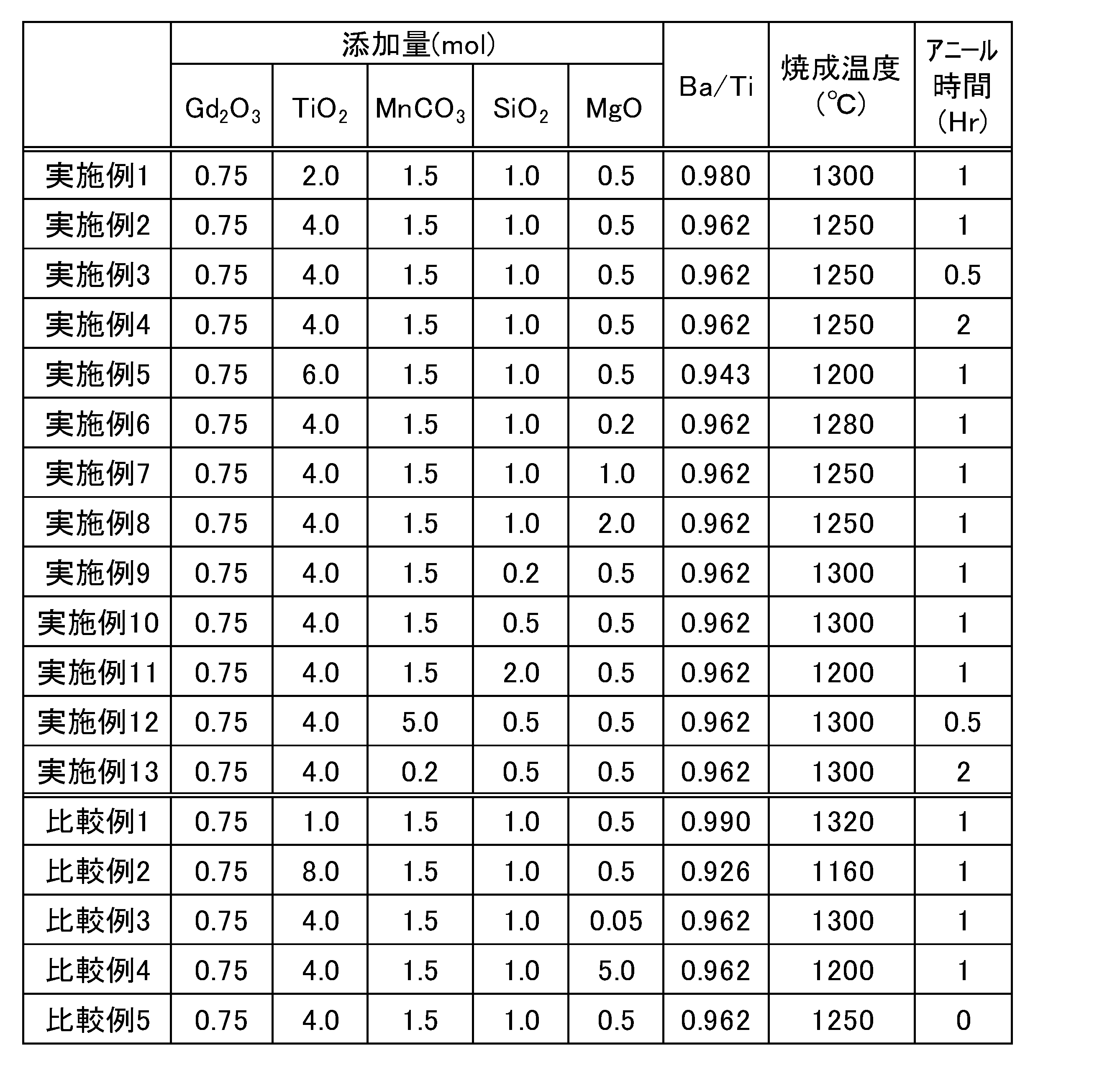
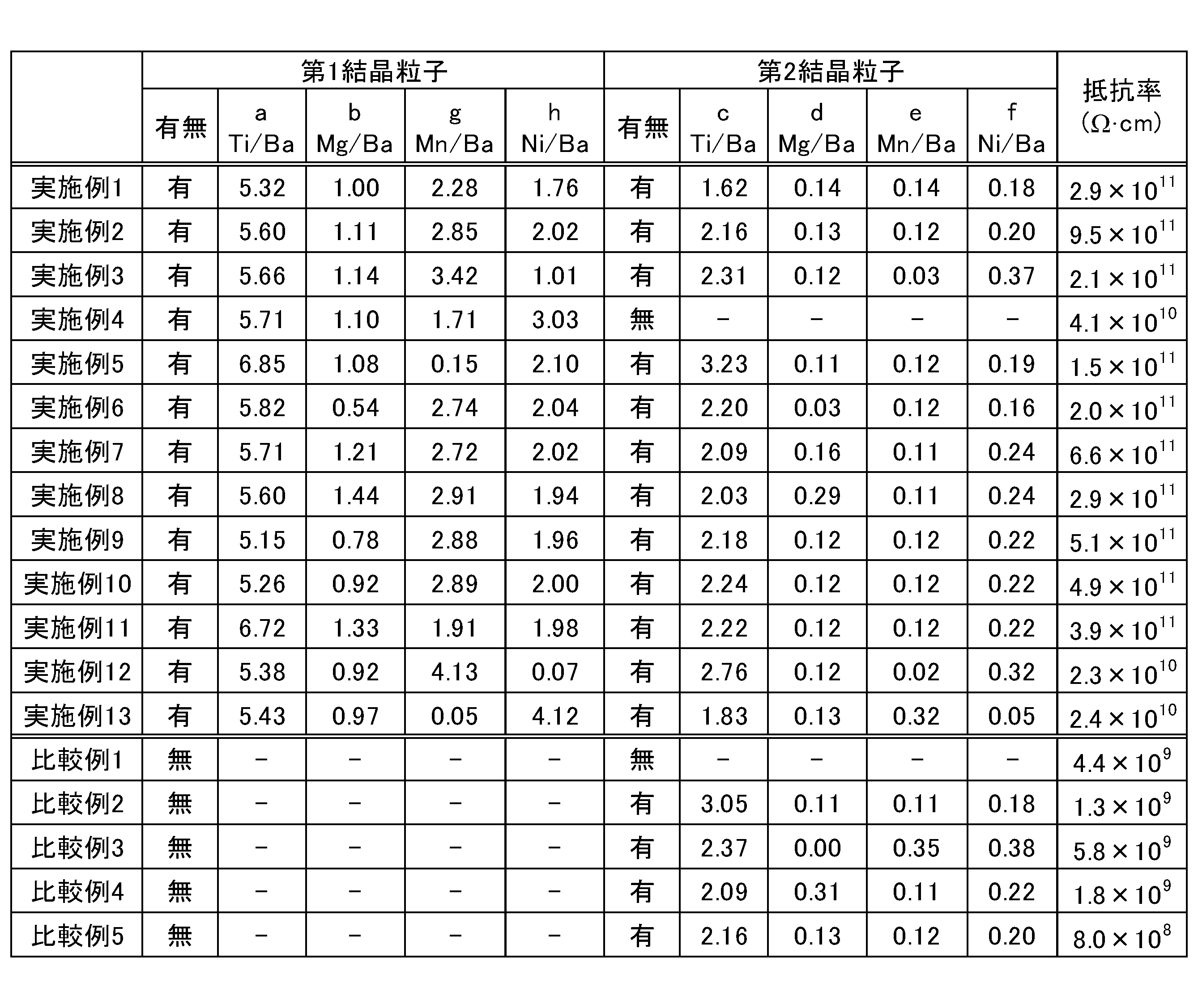
11 誘電体層
12 内部電極層
13 カバー層
14 容量領域
15 エンドマージン
16 サイドマージン
20a,20b 外部電極
40 主相結晶粒子
41 第1結晶粒子
42 第2結晶粒子
43 第3結晶粒子
44 空隙
51 セラミックグリーンシート
52 内部電極パターン
53 誘電体パターン
54 カバーシート
55 サイドマージン部
100 積層セラミックコンデンサ
Claims (13)
- ペロブスカイト型構造を有するチタン酸バリウムを含む主相と、
バリウム、チタン、およびマグネシウムを含み、バリウムの含有量に対するチタンの元素比率をa、バリウムの含有量に対するマグネシウムの元素比率をbとしたとき、5.00≦a≦7.00であり、0.50≦b≦1.50を満たす第1結晶粒子と、
バリウム、チタン、マグネシウム、マンガン、およびニッケルを含み、バリウムの含有量に対するチタンの元素比率をc、バリウムの含有量に対するマグネシウムの元素比率をd、バリウムの含有量に対するマンガンの元素比率をe、バリウムの含有量に対するニッケルの元素比率をfとしたとき、1.50≦c≦3.50であり、0.03≦d≦0.30であり、0.03≦e≦0.30であり、0.03≦f≦0.40を満たす第2結晶粒子と、を有する、誘電体磁器組成物。 - 前記第1結晶粒子は、さらにマンガンおよびニッケルを含み、
前記第1結晶粒子において、バリウムの含有量に対するマンガンの元素比率をg、バリウムの含有量に対するニッケルの元素比率をhとしたとき、0.10≦g≦4.00であり、0.10≦h≦4.00を満たす、請求項1に記載の誘電体磁器組成物。 - シリケート、エンスタテイト、バリウムマグネシウムシリケート、またはフレスノイトの少なくとも1つを含む第3結晶粒子をさらに含む、請求項1に記載の誘電体磁器組成物。
- 前記第1結晶粒子および前記第2結晶粒子は、前記主相の粒界に位置する、請求項1に記載の誘電体磁器組成物。
- 前記第1結晶粒子および前記第2結晶粒子は、前記主相の粒界三重点に位置する、請求項1に記載の誘電体磁器組成物。
- 前記第3結晶粒子は、前記主相の粒界に位置する、請求項3に記載の誘電体磁器組成物。
- 前記第3結晶粒子は、前記主相の粒界三重点に位置する、請求項3に記載の誘電体磁器組成物。
- 前記主相は、コア部と、前記コア部を覆うシェル部と、を有する、請求項1に記載の誘電体磁器組成物。
- 前記シェル部に希土類元素を含む、請求項8に記載の誘電体磁器組成物。
- チタンに対するバリウムの元素比率が0.940以上0.980以下であり、チタンに対するガドリニウムの元素比率が0.005以上0.05以下であり、チタンに対するマグネシウムの元素比率が0.002以上0.02以下である、請求項1に記載の誘電体磁器組成物。
- ペロブスカイト型構造を有し、チタン酸バリウムを含み、コア部および前記コア部を覆うシェル部を有する主相と、
バリウム、チタン、およびマグネシウムを含み、バリウムの含有量に対するチタンの元素比率をa、バリウムの含有量に対するマグネシウムの元素比率をbとしたとき、5.00≦a≦7.00であり、0.50≦b≦1.50を満たす第1結晶粒子と、を有する、誘電体磁器組成物。 - 前記第1結晶粒子は、さらにマンガンおよびニッケルを含み、
前記第1結晶粒子において、バリウムの含有量に対するマンガンの元素比率をg、バリウムの含有量に対するニッケルの元素比率をhとしたとき、0.10≦g≦4.00であり、0.10≦h≦4.00を満たす、請求項11に記載の誘電体磁器組成物。 - 請求項1に記載の誘電体磁器組成物を含む複数の誘電体層と、
前記複数の誘電体層を挟んで互いに対向する複数の内部電極と、
前記複数の内部電極に電気的に接続される外部電極と、を有する、積層セラミック電子部品。
Priority Applications (4)
| Application Number | Priority Date | Filing Date | Title |
|---|---|---|---|
| CN202480023359.2A CN120897899A (zh) | 2023-03-29 | 2024-03-12 | 介电陶瓷组合物和层叠陶瓷电子部件 |
| KR1020257031827A KR20250170038A (ko) | 2023-03-29 | 2024-03-12 | 유전체 자기 조성물 및 적층 세라믹 전자 부품 |
| DE112024000676.0T DE112024000676T5 (de) | 2023-03-29 | 2024-03-12 | Dielektrische keramikzusammensetzung und elektronisches mehrschicht-keramikbauteil |
| JP2025510262A JPWO2024203277A1 (ja) | 2023-03-29 | 2024-03-12 |
Applications Claiming Priority (2)
| Application Number | Priority Date | Filing Date | Title |
|---|---|---|---|
| JP2023053844 | 2023-03-29 | ||
| JP2023-053844 | 2023-03-29 |
Publications (1)
| Publication Number | Publication Date |
|---|---|
| WO2024203277A1 true WO2024203277A1 (ja) | 2024-10-03 |
Family
ID=92904580
Family Applications (1)
| Application Number | Title | Priority Date | Filing Date |
|---|---|---|---|
| PCT/JP2024/009537 Ceased WO2024203277A1 (ja) | 2023-03-29 | 2024-03-12 | 誘電体磁器組成物および積層セラミック電子部品 |
Country Status (5)
| Country | Link |
|---|---|
| JP (1) | JPWO2024203277A1 (ja) |
| KR (1) | KR20250170038A (ja) |
| CN (1) | CN120897899A (ja) |
| DE (1) | DE112024000676T5 (ja) |
| WO (1) | WO2024203277A1 (ja) |
Citations (4)
| Publication number | Priority date | Publication date | Assignee | Title |
|---|---|---|---|---|
| JP2001230149A (ja) * | 2000-02-16 | 2001-08-24 | Taiyo Yuden Co Ltd | 積層セラミックコンデンサとその製造方法 |
| WO2008038722A1 (fr) * | 2006-09-27 | 2008-04-03 | Kyocera Corporation | Condensateur multicouche en céramique et procédé de production correspondant |
| WO2014002302A1 (ja) * | 2012-06-29 | 2014-01-03 | 太陽誘電株式会社 | 積層セラミックコンデンサ |
| JP2022181544A (ja) * | 2021-05-26 | 2022-12-08 | Tdk株式会社 | 誘電体組成物および積層セラミック電子部品。 |
Family Cites Families (2)
| Publication number | Priority date | Publication date | Assignee | Title |
|---|---|---|---|---|
| JP5932216B2 (ja) | 2010-12-22 | 2016-06-08 | キヤノン株式会社 | 圧電セラミックス、その製造方法、圧電素子、液体吐出ヘッド、超音波モータ、塵埃除去装置、光学デバイスおよび電子機器 |
| US9614141B2 (en) | 2015-01-09 | 2017-04-04 | Canon Kabushiki Kaisha | Piezoelectric ceramic, piezoelectric element, piezoelectric device and piezoelectric ceramic manufacturing method |
-
2024
- 2024-03-12 DE DE112024000676.0T patent/DE112024000676T5/de active Pending
- 2024-03-12 JP JP2025510262A patent/JPWO2024203277A1/ja active Pending
- 2024-03-12 WO PCT/JP2024/009537 patent/WO2024203277A1/ja not_active Ceased
- 2024-03-12 CN CN202480023359.2A patent/CN120897899A/zh active Pending
- 2024-03-12 KR KR1020257031827A patent/KR20250170038A/ko active Pending
Patent Citations (4)
| Publication number | Priority date | Publication date | Assignee | Title |
|---|---|---|---|---|
| JP2001230149A (ja) * | 2000-02-16 | 2001-08-24 | Taiyo Yuden Co Ltd | 積層セラミックコンデンサとその製造方法 |
| WO2008038722A1 (fr) * | 2006-09-27 | 2008-04-03 | Kyocera Corporation | Condensateur multicouche en céramique et procédé de production correspondant |
| WO2014002302A1 (ja) * | 2012-06-29 | 2014-01-03 | 太陽誘電株式会社 | 積層セラミックコンデンサ |
| JP2022181544A (ja) * | 2021-05-26 | 2022-12-08 | Tdk株式会社 | 誘電体組成物および積層セラミック電子部品。 |
Also Published As
| Publication number | Publication date |
|---|---|
| DE112024000676T5 (de) | 2025-11-20 |
| JPWO2024203277A1 (ja) | 2024-10-03 |
| KR20250170038A (ko) | 2025-12-04 |
| CN120897899A (zh) | 2025-11-04 |
Similar Documents
| Publication | Publication Date | Title |
|---|---|---|
| US7652870B2 (en) | Multilayer ceramic capacitor | |
| CN102483993B (zh) | 层叠陶瓷电容器的制造方法以及层叠陶瓷电容器 | |
| TWI525651B (zh) | Laminated ceramic capacitors | |
| US7638451B2 (en) | Dielectric ceramic, method of producing the same, and monolithic ceramic capacitor | |
| TWI401235B (zh) | Dielectric ceramics and laminated ceramic capacitors | |
| JP7649598B2 (ja) | 誘電体、積層セラミックコンデンサ、誘電体の製造方法、および積層セラミックコンデンサの製造方法 | |
| JP7186014B2 (ja) | 積層セラミックコンデンサおよびその製造方法 | |
| JP5998765B2 (ja) | 誘電体磁器組成物およびこれを用いたセラミック電子部品 | |
| US20250259790A1 (en) | Multilayer ceramic capacitor | |
| JP2019161217A (ja) | 積層セラミックコンデンサおよびセラミック原料粉末 | |
| JP4552419B2 (ja) | 誘電体セラミックおよび積層セラミックコンデンサ | |
| CN107851513A (zh) | 介电组成、介电元件、电子部件和多层电子部件 | |
| TW202305845A (zh) | 陶瓷電子零件及其製造方法 | |
| JP5094283B2 (ja) | 誘電体磁器および積層セラミックコンデンサ | |
| JP7441110B2 (ja) | 誘電体、電子部品、および積層セラミックコンデンサ | |
| US12374492B2 (en) | Multilayer electronic component and method of manufacturing the same | |
| US20240409470A1 (en) | Dielectric ceramic composition and multilayer ceramic electronic device | |
| JP7262640B2 (ja) | セラミックコンデンサ | |
| WO2024203277A1 (ja) | 誘電体磁器組成物および積層セラミック電子部品 | |
| JP7536434B2 (ja) | セラミック電子部品の製造方法、およびシート部材 | |
| US20260120951A1 (en) | Multilayer ceramic electronic component and dielectric ceramic composition | |
| US20250239402A1 (en) | Multilayer ceramic electronic device and dielectric ceramic composition | |
| US20250182970A1 (en) | Multilayer ceramic electronic device and dielectric ceramic composition | |
| WO2024171939A1 (ja) | 誘電体磁器組成物および積層セラミック電子部品 | |
| US20240404754A1 (en) | Dielectric ceramic composition and multilayer ceramic electronic device |
Legal Events
| Date | Code | Title | Description |
|---|---|---|---|
| 121 | Ep: the epo has been informed by wipo that ep was designated in this application |
Ref document number: 24779407 Country of ref document: EP Kind code of ref document: A1 |
|
| ENP | Entry into the national phase |
Ref document number: 2025510262 Country of ref document: JP Kind code of ref document: A |
|
| WWE | Wipo information: entry into national phase |
Ref document number: 2025510262 Country of ref document: JP |
|
| ENP | Entry into the national phase |
Ref document number: 1020257031827 Country of ref document: KR Free format text: ST27 STATUS EVENT CODE: A-0-1-A10-A15-NAP-PA0105 (AS PROVIDED BY THE NATIONAL OFFICE) |
|
| WWE | Wipo information: entry into national phase |
Ref document number: KR1020257031827 Country of ref document: KR |
|
| WWE | Wipo information: entry into national phase |
Ref document number: 112024000676 Country of ref document: DE |
|
| WWE | Wipo information: entry into national phase |
Ref document number: CN2024800233592 Country of ref document: CN Ref document number: 202480023359.2 Country of ref document: CN |
|
| WWP | Wipo information: published in national office |
Ref document number: 202480023359.2 Country of ref document: CN |
|
| 122 | Ep: pct application non-entry in european phase |
Ref document number: 24779407 Country of ref document: EP Kind code of ref document: A1 |