WO2024202941A1 - 半導体装置 - Google Patents
半導体装置 Download PDFInfo
- Publication number
- WO2024202941A1 WO2024202941A1 PCT/JP2024/007832 JP2024007832W WO2024202941A1 WO 2024202941 A1 WO2024202941 A1 WO 2024202941A1 JP 2024007832 W JP2024007832 W JP 2024007832W WO 2024202941 A1 WO2024202941 A1 WO 2024202941A1
- Authority
- WO
- WIPO (PCT)
- Prior art keywords
- region
- trench
- semiconductor
- main surface
- insulating film
- Prior art date
- Legal status (The legal status is an assumption and is not a legal conclusion. Google has not performed a legal analysis and makes no representation as to the accuracy of the status listed.)
- Ceased
Links
Images
















Classifications
-
- H—ELECTRICITY
- H10—SEMICONDUCTOR DEVICES; ELECTRIC SOLID-STATE DEVICES NOT OTHERWISE PROVIDED FOR
- H10D—INORGANIC ELECTRIC SEMICONDUCTOR DEVICES
- H10D30/00—Field-effect transistors [FET]
- H10D30/60—Insulated-gate field-effect transistors [IGFET]
- H10D30/601—Insulated-gate field-effect transistors [IGFET] having lightly-doped drain or source extensions, e.g. LDD IGFETs or DDD IGFETs
- H10D30/608—Insulated-gate field-effect transistors [IGFET] having lightly-doped drain or source extensions, e.g. LDD IGFETs or DDD IGFETs having non-planar bodies, e.g. having recessed gate electrodes
-
- H—ELECTRICITY
- H10—SEMICONDUCTOR DEVICES; ELECTRIC SOLID-STATE DEVICES NOT OTHERWISE PROVIDED FOR
- H10D—INORGANIC ELECTRIC SEMICONDUCTOR DEVICES
- H10D84/00—Integrated devices formed in or on semiconductor substrates that comprise only semiconducting layers, e.g. on Si wafers or on GaAs-on-Si wafers
- H10D84/101—Integrated devices comprising main components and built-in components, e.g. IGBT having built-in freewheel diode
- H10D84/141—VDMOS having built-in components
- H10D84/143—VDMOS having built-in components the built-in components being PN junction diodes
- H10D84/144—VDMOS having built-in components the built-in components being PN junction diodes in antiparallel diode configurations
-
- H—ELECTRICITY
- H10—SEMICONDUCTOR DEVICES; ELECTRIC SOLID-STATE DEVICES NOT OTHERWISE PROVIDED FOR
- H10D—INORGANIC ELECTRIC SEMICONDUCTOR DEVICES
- H10D30/00—Field-effect transistors [FET]
- H10D30/01—Manufacture or treatment
- H10D30/021—Manufacture or treatment of FETs having insulated gates [IGFET]
- H10D30/0217—Manufacture or treatment of FETs having insulated gates [IGFET] forming self-aligned punch-through stoppers or threshold implants under gate regions
-
- H—ELECTRICITY
- H10—SEMICONDUCTOR DEVICES; ELECTRIC SOLID-STATE DEVICES NOT OTHERWISE PROVIDED FOR
- H10D—INORGANIC ELECTRIC SEMICONDUCTOR DEVICES
- H10D30/00—Field-effect transistors [FET]
- H10D30/01—Manufacture or treatment
- H10D30/021—Manufacture or treatment of FETs having insulated gates [IGFET]
- H10D30/027—Manufacture or treatment of FETs having insulated gates [IGFET] of lateral single-gate IGFETs
-
- H—ELECTRICITY
- H10—SEMICONDUCTOR DEVICES; ELECTRIC SOLID-STATE DEVICES NOT OTHERWISE PROVIDED FOR
- H10D—INORGANIC ELECTRIC SEMICONDUCTOR DEVICES
- H10D62/00—Semiconductor bodies, or regions thereof, of devices having potential barriers
- H10D62/10—Shapes, relative sizes or dispositions of the regions of the semiconductor bodies; Shapes of the semiconductor bodies
- H10D62/124—Shapes, relative sizes or dispositions of the regions of semiconductor bodies or of junctions between the regions
- H10D62/126—Top-view geometrical layouts of the regions or the junctions
- H10D62/127—Top-view geometrical layouts of the regions or the junctions of cellular field-effect devices, e.g. multicellular DMOS transistors or IGBTs
-
- H—ELECTRICITY
- H10—SEMICONDUCTOR DEVICES; ELECTRIC SOLID-STATE DEVICES NOT OTHERWISE PROVIDED FOR
- H10D—INORGANIC ELECTRIC SEMICONDUCTOR DEVICES
- H10D62/00—Semiconductor bodies, or regions thereof, of devices having potential barriers
- H10D62/10—Shapes, relative sizes or dispositions of the regions of the semiconductor bodies; Shapes of the semiconductor bodies
- H10D62/17—Semiconductor regions connected to electrodes not carrying current to be rectified, amplified or switched, e.g. channel regions
- H10D62/213—Channel regions of field-effect devices
- H10D62/221—Channel regions of field-effect devices of FETs
- H10D62/235—Channel regions of field-effect devices of FETs of IGFETs
- H10D62/299—Channel regions of field-effect devices of FETs of IGFETs having lateral doping variations
- H10D62/307—Channel regions of field-effect devices of FETs of IGFETs having lateral doping variations the doping variations being parallel to the channel lengths
-
- H—ELECTRICITY
- H10—SEMICONDUCTOR DEVICES; ELECTRIC SOLID-STATE DEVICES NOT OTHERWISE PROVIDED FOR
- H10D—INORGANIC ELECTRIC SEMICONDUCTOR DEVICES
- H10D62/00—Semiconductor bodies, or regions thereof, of devices having potential barriers
- H10D62/10—Shapes, relative sizes or dispositions of the regions of the semiconductor bodies; Shapes of the semiconductor bodies
- H10D62/17—Semiconductor regions connected to electrodes not carrying current to be rectified, amplified or switched, e.g. channel regions
- H10D62/351—Substrate regions of field-effect devices
- H10D62/357—Substrate regions of field-effect devices of FETs
- H10D62/364—Substrate regions of field-effect devices of FETs of IGFETs
- H10D62/378—Contact regions to the substrate regions
-
- H—ELECTRICITY
- H10—SEMICONDUCTOR DEVICES; ELECTRIC SOLID-STATE DEVICES NOT OTHERWISE PROVIDED FOR
- H10D—INORGANIC ELECTRIC SEMICONDUCTOR DEVICES
- H10D64/00—Electrodes of devices having potential barriers
- H10D64/20—Electrodes characterised by their shapes, relative sizes or dispositions
- H10D64/23—Electrodes carrying the current to be rectified, amplified, oscillated or switched, e.g. sources, drains, anodes or cathodes
- H10D64/251—Source or drain electrodes for field-effect devices
- H10D64/256—Source or drain electrodes for field-effect devices for lateral devices wherein the source or drain electrodes are recessed in semiconductor bodies
-
- H—ELECTRICITY
- H10—SEMICONDUCTOR DEVICES; ELECTRIC SOLID-STATE DEVICES NOT OTHERWISE PROVIDED FOR
- H10D—INORGANIC ELECTRIC SEMICONDUCTOR DEVICES
- H10D64/00—Electrodes of devices having potential barriers
- H10D64/20—Electrodes characterised by their shapes, relative sizes or dispositions
- H10D64/27—Electrodes not carrying the current to be rectified, amplified, oscillated or switched, e.g. gates
- H10D64/311—Gate electrodes for field-effect devices
- H10D64/411—Gate electrodes for field-effect devices for FETs
- H10D64/511—Gate electrodes for field-effect devices for FETs for IGFETs
- H10D64/512—Disposition of the gate electrodes, e.g. buried gates
- H10D64/513—Disposition of the gate electrodes, e.g. buried gates within recesses in the substrate, e.g. trench gates, groove gates or buried gates
-
- H—ELECTRICITY
- H10—SEMICONDUCTOR DEVICES; ELECTRIC SOLID-STATE DEVICES NOT OTHERWISE PROVIDED FOR
- H10D—INORGANIC ELECTRIC SEMICONDUCTOR DEVICES
- H10D64/00—Electrodes of devices having potential barriers
- H10D64/20—Electrodes characterised by their shapes, relative sizes or dispositions
- H10D64/27—Electrodes not carrying the current to be rectified, amplified, oscillated or switched, e.g. gates
- H10D64/311—Gate electrodes for field-effect devices
- H10D64/411—Gate electrodes for field-effect devices for FETs
- H10D64/511—Gate electrodes for field-effect devices for FETs for IGFETs
- H10D64/517—Gate electrodes for field-effect devices for FETs for IGFETs characterised by the conducting layers
- H10D64/519—Gate electrodes for field-effect devices for FETs for IGFETs characterised by the conducting layers characterised by their top-view geometrical layouts
-
- H—ELECTRICITY
- H10—SEMICONDUCTOR DEVICES; ELECTRIC SOLID-STATE DEVICES NOT OTHERWISE PROVIDED FOR
- H10D—INORGANIC ELECTRIC SEMICONDUCTOR DEVICES
- H10D84/00—Integrated devices formed in or on semiconductor substrates that comprise only semiconducting layers, e.g. on Si wafers or on GaAs-on-Si wafers
- H10D84/01—Manufacture or treatment
- H10D84/0107—Integrating at least one component covered by H10D12/00 or H10D30/00 with at least one component covered by H10D8/00, H10D10/00 or H10D18/00, e.g. integrating IGFETs with BJTs
- H10D84/0109—Integrating at least one component covered by H10D12/00 or H10D30/00 with at least one component covered by H10D8/00, H10D10/00 or H10D18/00, e.g. integrating IGFETs with BJTs the at least one component covered by H10D12/00 or H10D30/00 being a MOS device
-
- H—ELECTRICITY
- H10—SEMICONDUCTOR DEVICES; ELECTRIC SOLID-STATE DEVICES NOT OTHERWISE PROVIDED FOR
- H10D—INORGANIC ELECTRIC SEMICONDUCTOR DEVICES
- H10D62/00—Semiconductor bodies, or regions thereof, of devices having potential barriers
- H10D62/40—Crystalline structures
- H10D62/405—Orientations of crystalline planes
-
- H—ELECTRICITY
- H10—SEMICONDUCTOR DEVICES; ELECTRIC SOLID-STATE DEVICES NOT OTHERWISE PROVIDED FOR
- H10D—INORGANIC ELECTRIC SEMICONDUCTOR DEVICES
- H10D62/00—Semiconductor bodies, or regions thereof, of devices having potential barriers
- H10D62/80—Semiconductor bodies, or regions thereof, of devices having potential barriers characterised by the materials
- H10D62/83—Semiconductor bodies, or regions thereof, of devices having potential barriers characterised by the materials being Group IV materials, e.g. B-doped Si or undoped Ge
- H10D62/832—Semiconductor bodies, or regions thereof, of devices having potential barriers characterised by the materials being Group IV materials, e.g. B-doped Si or undoped Ge being Group IV materials comprising two or more elements, e.g. SiGe
- H10D62/8325—Silicon carbide
Definitions
- This disclosure relates to a semiconductor device.
- Patent Document 1 discloses a semiconductor device including a semiconductor chip having a first main surface, an n-type drift layer formed on a surface portion of the first main surface, a trench gate structure formed on the first main surface so as to contact the drift layer, a p-type channel region formed in the drift layer so as to cover the sidewall of the trench gate structure, and a first source/drain region and a second source/drain region formed at an interval in the drift layer in a region along the sidewall of the trench gate structure so as to face each other across the channel region.
- One embodiment of the present disclosure provides a semiconductor device that can simplify the manufacturing process.
- One embodiment of the present disclosure provides an in-hand device including a semiconductor chip consisting of a single layer having a first main surface and a second main surface opposite the first main surface, a first semiconductor region of a first conductivity type formed on the first main surface side of the semiconductor chip, a second semiconductor region of a second conductivity type formed on the second main surface side of the first semiconductor region of the semiconductor chip, a first trench penetrating the first semiconductor region from the first main surface and dividing the first semiconductor region into a first region on one side and a second region on the other side in a cross-sectional view, a control insulating film covering an inner wall of the first trench, and a control electrode embedded in the first trench across the control insulating film and controlling a channel in the second semiconductor region that connects the first region and the second region in the lateral direction along the first main surface.
- a semiconductor device can be provided that can simplify the manufacturing process.
- FIG. 1 is a circuit diagram of a semiconductor device according to a first embodiment of the present disclosure.
- FIG. 2 is a schematic perspective view of the semiconductor device according to the first embodiment of the present disclosure.
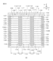
- FIG. 3 is a plan view of the semiconductor device of FIG.
- FIG. 4 is a plan view showing the internal structure of the semiconductor device of FIG.
- FIG. 5 is a plan view showing the internal structure of the semiconductor device of FIG.
- FIG. 6 is a plan view showing the internal structure of the semiconductor device of FIG.
- FIG. 7 is a plan view showing the internal structure of the semiconductor device of FIG.
- FIG. 8 is an enlarged view of a portion surrounded by a two-dot chain line VIII in FIG.
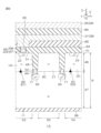
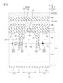
- FIG. 9 is a cross-sectional view taken along line IX-IX in FIG.
- FIG. 9 is a cross-sectional view taken along line IX-IX in FIG.
- FIG. 9 is a cross-sectional view taken along line IX-IX in FIG. FIG.
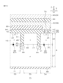
- FIG. 10 is a cross-sectional view taken along line XX in FIG.
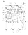
- FIG. 11 is a cross-sectional view taken along line XI-XI in FIG.
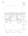
- FIG. 12 is a cross-sectional view taken along line XII-XII in FIG.
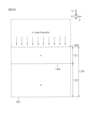
- FIG. 13A is a diagram showing a part of the manufacturing process of the semiconductor device according to the first embodiment of the present disclosure.
- FIG. 13B is a diagram showing the next step of FIG. 13A.
- FIG. 13C is a diagram showing the next step of FIG. 13B.
- FIG. 13D is a diagram showing the next step of FIG. 13C.
- FIG. 13E is a diagram showing the next step of FIG. 13D.
- FIG. 13F is a diagram showing the next step of FIG. 13E.
- FIG. 13A is a diagram showing a part of the manufacturing process of the semiconductor device according to the first embodiment of the present disclosure.
- FIG. 13B is a diagram showing the next step of FIG. 13
- FIG. 13G is a diagram showing the next step of FIG. 13F.
- FIG. 13H is a diagram showing the next step of FIG. 13G.
- FIG. 13I is a diagram showing the next step of FIG. 13H.
- FIG. 13J is a diagram showing the next step of FIG. 13I.
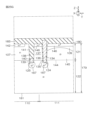
- FIG. 14 is a cross-sectional view showing a current path of the semiconductor device according to the first embodiment of the present disclosure.
- FIG. 15 is a plan view showing a current path of the semiconductor device according to the first embodiment of the present disclosure.
- FIG. 16 is a cross-sectional view showing a first modified example of the semiconductor device according to the first embodiment of the present disclosure.
- FIG. 17 is a cross-sectional view showing a second modification of the semiconductor device according to the first embodiment of the present disclosure.
- FIG. 14 is a cross-sectional view showing a current path of the semiconductor device according to the first embodiment of the present disclosure.
- FIG. 15 is a plan view showing a current path of the semiconductor
- FIG. 18 is a cross-sectional view showing a third modified example of the semiconductor device according to the first embodiment of the present disclosure.
- FIG. 19 is a schematic plan view showing the internal structure of a semiconductor device according to a second embodiment of the present disclosure.
- FIG. 20 is an enlarged view of a portion surrounded by a two-dot chain line XX in FIG.
- FIG. 21 is an enlarged view of a portion surrounded by a two-dot chain line XX in FIG.
- FIG. 22 is a cross-sectional view taken along line XXII-XXII in FIG.
- FIG. 23 is a cross-sectional view taken along line XXIII-XXIII in FIG.
- FIG. 25A is a diagram showing a part of a manufacturing process of a semiconductor device according to the second embodiment of the present disclosure.
- FIG. 25B is a diagram showing the next step of FIG. 25A.
- FIG. 25C is a diagram showing the next step of FIG. 25B.
- FIG. 25D is a diagram showing the next step of FIG. 25C.
- FIG. 25E is a diagram showing the next step of FIG. 25D.
- FIG. 25F is a diagram showing the next step of FIG. 25E.
- FIG. 25G is a diagram showing the next step of FIG. 25F.
- FIG. 25H is a diagram showing the next step of FIG. 25G.
- FIG. 25A is a diagram showing a part of a manufacturing process of a semiconductor device according to the second embodiment of the present disclosure.
- FIG. 25B is a diagram showing the next step of FIG. 25A.
- FIG. 25C is a diagram showing the next step of FIG. 25B.
- FIG. 25D is
- FIG. 25I is a diagram showing the next step of FIG. 25H.
- FIG. 25J is a diagram showing the next step of FIG. 25I.
- FIG. 26 is a cross-sectional view showing a current path of a semiconductor device according to a second embodiment of the present disclosure.
- FIG. 27 is a plan view showing a current path of the semiconductor device according to the second embodiment of the present disclosure.
- FIG. 28 is a diagram for explaining the effect of improving the breakdown voltage of the semiconductor device according to the second embodiment of the present disclosure.
- FIG. 29 is a diagram for explaining the effect of improving the breakdown voltage of the semiconductor device according to the second embodiment of the present disclosure.
- FIG. 30 is a diagram for explaining the effect of improving the breakdown voltage of the semiconductor device according to the second embodiment of the present disclosure.
- FIG. 26 is a cross-sectional view showing a current path of a semiconductor device according to a second embodiment of the present disclosure.
- FIG. 27 is a plan view showing a current path of the semiconductor device according to the second
- FIG. 31 is a diagram for explaining the effect of improving the breakdown voltage of the semiconductor device according to the second embodiment of the present disclosure.
- FIG. 32 is a diagram for explaining the effect of improving the breakdown voltage of the semiconductor device according to the second embodiment of the present disclosure.
- FIG. 33 is a cross-sectional view showing a first modified example of the semiconductor device according to the second embodiment of the present disclosure.
- FIG. 34 is a cross-sectional view showing a second modification of the semiconductor device according to the second embodiment of the present disclosure.
- FIG. 35 is a cross-sectional view showing a third modified example of the semiconductor device according to the second embodiment of the present disclosure.
- FIG. 1 is a circuit diagram of a semiconductor device 1A according to a first embodiment of the present disclosure.
- the semiconductor device 1A includes a common source-drain type MISFET (Metal Insulator Semiconductor Field Effect Transistor) 2.
- the MISFET 2 includes a base B, a gate G, a first source-drain SD1, and a second source-drain SD2.
- the first source-drain SD1 and the second source-drain SD2 serve as both a source and a drain.
- the first source-drain SD1 may be the source and the second source-drain SD2 may be the drain.
- the first source-drain SD1 may be the drain and the second source-drain SD2 may be the source.
- a reference voltage (for example, a ground voltage) is applied to the base B.
- a gate voltage VG based on the base B is applied to the gate G.
- the gate G controls the conduction and blocking of the current I flowing between the first source drain SD1 and the second source drain SD2.
- a first source drain voltage VSD1 (first voltage) is applied to the first source drain SD1.
- a second source drain voltage VSD2 (second voltage) different from the first source drain voltage VSD1 is applied to the second source drain SD2.
- the semiconductor device 1A further includes a diode pair 3 connected to the first source drain SD1 and the second source drain SD2.
- the diode pair 3 regulates (cuts off) the current I flowing between the first source drain SD1 and the second source drain SD2 when the MISFET 2 is in the off state.
- the diode pair 3 specifically includes a first body diode D1 and a second body diode D2 that are reverse-bias connected.
- the first body diode D1 and the second body diode D2 each include an anode and a cathode.
- the anode of the first body diode D1 is connected to the base B.
- the cathode of the first body diode D1 is connected to the first source drain SD1.
- the anode of the second body diode D2 is connected to the base B.
- the cathode of the second body diode D2 is connected to the second source drain SD2.
- the semiconductor device 1A is a four-terminal device including four external terminals 4, 5, 6, and 7.
- the external terminals 4 to 7 specifically include a base terminal 4, a gate terminal 5, a first source-drain terminal 6, and a second source-drain terminal 7.
- the base terminal 4 is connected to the base B.
- the gate terminal 5 is connected to the gate G.
- the first source-drain terminal 6 is connected to the first source-drain SD1.
- the second source-drain terminal 7 is connected to the second source-drain SD2.
- the MISFET 2 is a bidirectional device that can pass a current I in both directions between the first source drain terminal 6 and the second source drain terminal 7. That is, when the first source drain terminal 6 is connected to the high voltage side (input side), the second source drain terminal 7 is connected to the low voltage side (output side). On the other hand, when the first source drain terminal 6 is connected to the low voltage side (output side), the second source drain terminal 7 is connected to the high voltage side (input side).
- Semiconductor device 1A can realize the function of a circuit in which the drains of two non-common source-drain type MISFETs are connected to each other using a single MISFET 2. Therefore, semiconductor device 1A can achieve low on-resistance by shortening the current path.
- the specific structure of semiconductor device 1A will be described below.
- FIG. 2 is a schematic perspective view of a semiconductor device 1A according to a first embodiment of the present disclosure.
- FIG. 3 is a plan view of the semiconductor device 1A of FIG. 2.
- the semiconductor device 1A is a chip-size package having a package size equal to the size of the chip.
- the semiconductor device 1A has a layered structure including a semiconductor chip 8 and an insulating layer 9.
- the semiconductor chip 8 is formed in a rectangular parallelepiped shape.
- the semiconductor chip 8 includes a first main surface 10 on one side, a second main surface 11 on the other side, and side surfaces 12A, 12B, 12C, and 12D that connect the first main surface 10 and the second main surface 11.
- the side surfaces 12A to 12D specifically include the first side surface 12A, the second side surface 12B, the third side surface 12C, and the fourth side surface 12D.
- the insulating layer 9 is formed on the first main surface 10.
- the insulating layer 9 includes an insulating main surface 13 and insulating side surfaces 14A, 14B, 14C, and 14D.
- the insulating side surfaces 14A to 14D specifically include a first insulating side surface 14A, a second insulating side surface 14B, a third insulating side surface 14C, and a fourth insulating side surface 14D.
- the insulating side surfaces 14A to 14D extend from the periphery of the insulating main surface 13 toward the semiconductor chip 8 and are continuous with the side surfaces 12A to 12D.
- the insulating side surfaces 14A to 14D specifically are formed flush with the side surfaces 12A to 12D.
- the multiple external terminals 4 to 7 are formed on the insulating main surface 13.
- the multiple external terminals 4 to 7 are arranged in a matrix of 5 rows and 5 columns with gaps in the first direction X and the second direction Y.
- the base terminal 4 is arranged in the first column of the third row.
- the gate terminal 5 is arranged in the fifth column of the third row.
- the gate terminal 5 faces the base terminal 4 in the first direction X.
- the first source drain terminals 6 are arranged in the first to fifth columns of the first row and the first to fifth columns of the fourth row.
- the second source drain terminals 7 are arranged in the first to fifth columns of the second row and the first to fifth columns of the fifth row.
- the second source drain terminals 7 arranged in the second row face the first source drain terminals 6 arranged in the first row in a one-to-one correspondence in the second direction Y.
- the second source drain terminals 7 arranged in the fifth row face the first source drain terminals 6 arranged in the fourth row in a one-to-one correspondence in the second direction Y.
- spaces are provided in the second, third and fourth columns of the third row.
- Any one of the base terminal 4, gate terminal 5, first source drain terminal 6 and second source drain terminal 7 may be disposed in each space.
- An electrically open terminal may be disposed in each space.
- the number and arrangement of the base terminals 4, gate terminals 5, first source drain terminals 6 and second source drain terminals 7 are arbitrary and are not limited to the number and arrangement shown in Figures 2 and 3.
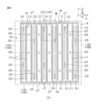
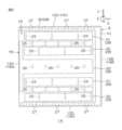
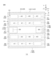
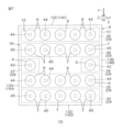
- FIGS. 4 to 7 are plan views showing the internal structure of the semiconductor device 1A in FIG. 2.
- FIG. 4 shows the planar structure of the semiconductor chip 8
- FIGS. 5 to 7 show the wiring pattern inside the insulating layer 9.
- an active area 15 and a peripheral area 16 surrounding the active area 15 are defined on the first main surface 10 of the semiconductor chip 8.
- the outer peripheral region 16 may coincide with the annular periphery along the side surfaces 12A-12D of the semiconductor chip 8.
- the outer peripheral region 16 may be an annular region extending from the side surfaces 12A-12D of the semiconductor chip 8 to a position approximately several ⁇ m inward.
- the active region 15 may be a central region of the semiconductor chip 8 surrounded by the outer peripheral region 16.
- the active region 15 may be, for example, a region in which most of the element structure of the MISFET 2 is formed.
- the active region 15 has a MISFET 2 element structure formed therein.
- the element structure is a trench-gate lateral type MISFET (Metal Insulator Semiconductor Field Effect Transistor) structure.
- MISFET2 includes a first trench structure 17 and a trench connection structure 18 as trench structures formed on the first main surface 10.
- the first trench structure 17 may be referred to as a "trench gate structure.”
- the multiple first trench structures 17 are each formed in the inner portion of the first main surface 10 at a distance from the periphery of the first main surface 10.
- the multiple first trench structures 17 are arranged at intervals in the first direction X, and each formed in a band shape extending in the second direction Y.
- the multiple first trench structures 17 are formed in a stripe shape extending in the second direction Y in a plan view.
- Each of the multiple first trench structures 17 has a first end on one side and a second end on the other side in the second direction Y.
- the trench connection structure 18 is connected to the first trench structure 17.
- the multiple (two in this embodiment) trench connection structures 18 include a trench connection structure 18 on one side (the third side 12C side) that connects the first ends of the multiple first trench structures 17, and a trench connection structure 18 on the other side (the fourth side 12D side) that connects the second ends of the multiple first trench structures 17.
- the trench connection structure 18 is formed on the inside of the first main surface 10 at a distance from the periphery of the first main surface 10.
- the trench connection structure 18 is formed in a band shape extending in a direction (specifically, the first direction X) intersecting the direction in which the multiple first trench structures 17 extend, and is connected to first and second ends of the multiple first trench structures 17.
- a direction specifically, the first direction X
- multiple closed regions surrounded by a pair of first trench structures 17 and a pair of trench connection structures 18 are formed on the first main surface 10.
- Each of the multiple closed regions 19-21 is sandwiched between the first trench structures 17 in the first direction X, and is formed in a strip shape extending in the second direction Y.
- the multiple closed regions 19-21 are arranged in the first direction X, separated by the first trench structures 17, and are formed in a stripe shape as a whole.
- the multiple closed regions 19-21 may include a first source-drain region 19, a second source-drain region 20, and a drift region 21.
- first source drain region 19 and the second source drain region 20 face each other with the drift region 21 in between.
- a first trench structure 17 is formed between the first source drain region 19 and the drift region 21, and between the drift region 21 and the second source drain region 20, separating them.
- the first source drain regions 19 and the second source drain regions 20 are alternately arranged at intervals in the first direction X, such that the drift region 21 is sandwiched between adjacent first source drain regions 19 and second source drain regions 20.
- a set of the first source drain region 19, drift region 21, second source drain region 20, and drift region 21 is repeatedly arranged in the first direction X.
- a first contact region 22 is formed in the first source drain region 19.
- the first contact region 22 may be referred to as a "first source drain contact region.”
- a band-shaped first contact region 22 extending in the second direction Y is formed in the inner region of each first source drain region 19.
- the first contact region 22 has an annular outer edge in a portion spaced inward from the first trench structure 17 and the trench connection structure 18.
- a first lower contact 23 is formed in the first contact region 22.
- the first lower contact 23 may be referred to as a "first source drain contact.”
- a plurality of first lower contacts 23 are formed at intervals in the second direction Y.
- Each first lower contact 23 is formed in a rectangular shape in plan view that is long along the second direction Y. Only one first lower contact 23 may be formed in each first contact region 22.
- a second contact region 24 is formed in the second source drain region 20.
- the second contact region 24 may be referred to as a "second source drain contact region.”
- a band-shaped second contact region 24 extending in the second direction Y is formed in the inner region of each second source drain region 20.
- the second contact region 24 has an annular outer edge in a portion spaced inward from the first trench structure 17 and the trench connection structure 18.
- a second lower contact 25 is formed in the second contact region 24.
- the second lower contact 25 may be referred to as a "second source drain contact.”
- a plurality of second lower contacts 25 are formed at intervals in the second direction Y.
- Each second lower contact 25 is formed in a rectangular shape in plan view that is long along the second direction Y. Only one second lower contact 25 may be formed in each second contact region 24.
- a first base contact 26 is formed in the drift region 21.
- a plurality of first base contacts 26 are formed at intervals in the second direction Y.
- Each first base contact 26 is formed in a rectangular shape in a plan view that is long along the second direction Y. Only one first base contact 26 may be formed in each drift region 21.
- the first lower contact 23, the second lower contact 25, and the first base contact 26 are electrically isolated from each other and fixed to different potentials.
- the multiple first lower contacts 23, the multiple second lower contacts 25, and the multiple first base contacts 26 are discretely arranged on the first main surface 10.
- the multiple first lower contacts 23, the multiple second lower contacts 25, and the multiple first base contacts 26 are arranged with a regularity in which contacts of the same type (same potential) are aligned in the first direction X.
- a first gate contact 27 is formed in the trench connection structure 18.
- the multiple first gate contacts 27 are arranged at intervals in the first direction X.
- the multiple first gate contacts 27 may include a first gate contact 27 arranged at an intersection between the trench connection structure 18 and the first trench structure 17.
- the multiple first gate contacts 27 may be arranged in a position facing at least one of the first source drain region 19, the second source drain region 20, and the drift region 21 in the second direction Y.
- multiple wiring layers are formed on the first main surface 10 of the semiconductor chip 8, and the aforementioned multiple external terminals are connected to the uppermost layer of the multiple wiring layers.
- the multiple wiring layers form a multi-layer wiring structure, and include, for example, a first wiring layer 28 shown by a solid line in Figure 5 and a second wiring layer 29 shown by a solid line in Figure 6, in that order from the first main surface 10 upwards.
- the external terminals are connected to the second wiring layer 29, as shown in Figure 7.
- the first wiring layer 28 may be referred to as the "first metal”. With reference to FIG. 5, the first wiring layer 28 includes a first gate wiring layer 30, a first lower wiring layer 31, a second lower wiring layer 32, and a first base wiring layer 33.
- the first gate wiring layer 30, the first lower wiring layer 31, the second lower wiring layer 32, and the first base wiring layer 33 are wiring layers that are physically independent of one another.
- the first lower wiring layer 31 may be referred to as the "first lower source-drain wiring layer”.
- the second lower wiring layer 32 may be referred to as the "second lower source-drain wiring layer”.
- the first gate wiring layer 30 is formed along the outer peripheral region 16 of the semiconductor chip 8.
- the first gate wiring layer 30 has a shape that surrounds the active region 15.
- the first gate wiring layer 30 surrounds the active region 15 from three sides, and has a shape that is open on one side (the first side 12A in FIG. 5) of the sides 12A to 12D of the semiconductor chip 8.
- the first gate wiring layer 30 is formed by three straight line portions that run along the outer peripheral region 16. Of the three straight line portions, a pair of straight line portions that face each other in the second direction Y cover the multiple first gate contacts 27 and are connected to the multiple first gate contacts 27.
- the first lower wiring layer 31 is formed so as to cover the first lower contacts 23 and is connected to the first lower contacts 23.
- the first lower wiring layer 31 is formed in a band shape extending in the first direction X so as to collectively cover the multiple first lower contacts 23 that are aligned in a straight line in the first direction X.
- the second lower wiring layer 32 is formed to cover the second lower contacts 25 and is connected to the second lower contacts 25.
- the second lower wiring layer 32 is formed in a band shape extending in the first direction X so as to collectively cover the multiple second lower contacts 25 that are aligned in a straight line in the first direction X.
- the multiple first lower wiring layers 31 and the multiple second lower wiring layers 32 are arranged alternately at intervals in the second direction Y.
- two strip-shaped first lower wiring layers 31 and two strip-shaped second lower wiring layers 32 are formed in a stripe shape at intervals from each other.
- the first base wiring layer 33 is formed to cover the first base contacts 26 and is connected to the first base contacts 26.
- the first base wiring layer 33 is formed in a band shape extending in the first direction X so as to collectively cover the multiple first base contacts 26 that are aligned in a straight line in the first direction X.
- the band-shaped first base wiring layer 33 is disposed one by one in the region between the first lower wiring layer 31 and the second lower wiring layer 32. All the first base wiring layers 33 are collectively connected on the open side (first side surface 12A side) of the first gate wiring layer 30.
- the second wiring layer 29 may be referred to as the "second metal".
- the second wiring layer 29 includes a second gate wiring layer 34, a first upper wiring layer 35, a second upper wiring layer 36, and a second base wiring layer 37.
- the second gate wiring layer 34, the first upper wiring layer 35, the second upper wiring layer 36, and the second base wiring layer 37 are wiring layers that are physically independent of one another.
- the first upper wiring layer 35 may be referred to as the "first upper source drain wiring layer”.
- the second upper wiring layer 36 may be referred to as the "second upper source drain wiring layer”.
- the first wiring layer 28 is shown by a dashed line to clarify the relationship between the second wiring layer 29 and the first wiring layer 28.
- the second gate wiring layer 34 and the second base wiring layer 37 are each formed in a rectangular shape in a plan view.
- the second gate wiring layer 34 and the second base wiring layer 37 are formed in positions facing each other in the first direction X in the center of the semiconductor chip 8 in the second direction Y.
- the second gate wiring layer 34 is disposed near the first side surface 12A of the sides 12A to 12D of the semiconductor chip 8, and the second base wiring layer 37 is disposed near the opposite second side surface 12B.
- the second gate wiring layer 34 is connected to the first gate wiring layer 30 via a second gate contact 38.
- the second base wiring layer 37 is connected to the first base wiring layer 33 via a second base contact 39.
- the first upper wiring layer 35 is formed in a band shape extending along the first lower wiring layer 31, and covers the first lower wiring layer 31.
- the first upper wiring layer 35 is connected to the first lower wiring layer 31 via the first upper contacts 40.
- a plurality of first upper contacts 40 may be formed, arranged at intervals in the first direction X.
- the second upper wiring layer 36 is formed in a band shape extending along the second lower wiring layer 32, and covers the second lower wiring layer 32.
- the second upper wiring layer 36 is connected to the second lower wiring layer 32 via a second upper contact 41.
- a plurality of second upper contacts 41 may be formed and arranged at intervals in the first direction X.
- the multiple external terminals are arranged on the corresponding second wiring layer 29.
- the second wiring layer 29 is shown with a dashed line to clarify the relationship between the multiple external terminals and the second wiring layer 29.
- the gate terminal 5 is provided on the second gate wiring layer 34 and is connected to the second gate wiring layer 34 via a gate terminal contact 42.
- the base terminal 4 is provided on the second base wiring layer 37 and is connected to the second base wiring layer 37 via a base terminal contact 43.
- the multiple first source drain terminals 6 are arranged at intervals in the longitudinal direction of the strip-shaped first upper wiring layer 35. Each first source drain terminal 6 is connected to the first upper wiring layer 35 via a first terminal contact 44.
- the second source drain terminals 7 are arranged at intervals in the longitudinal direction of the strip-shaped second upper wiring layer 36. Each second source drain terminal 7 is connected to the second upper wiring layer 36 via a second terminal contact 45.
- FIG. 8 is an enlarged view of the portion surrounded by the two-dot chain line VIII in FIG. 4.
- FIG. 9 is a cross-sectional view taken along line IX-IX in FIG. 8.
- FIG. 10 is a cross-sectional view taken along line X-X in FIG. 8.
- FIG. 11 is a cross-sectional view taken along line XI-XI in FIG. 8.
- FIG. 12 is a cross-sectional view taken along line XII-XII in FIG. 8.
- the semiconductor device 1A includes a semiconductor chip 8.
- the semiconductor chip 8 is a semiconductor chip 8 consisting of a single layer.
- the semiconductor chip 8 consisting of a single layer is a single structure of a semiconductor substrate without an epitaxial layer.
- the semiconductor chip 8 includes a single crystal of Si (silicon) or a wide band gap semiconductor without an epitaxial layer.
- a wide band gap semiconductor is a semiconductor having a band gap exceeding the band gap of Si.
- the semiconductor chip 8 may be a Si chip or a SiC (silicon carbide) chip.
- the semiconductor device 1A includes a first semiconductor region 46 of n-type (first conductivity type) formed in a region on the first main surface 10 side in the semiconductor chip 8.
- the first semiconductor region 46 may be referred to as a "drift layer.”
- the first semiconductor region 46 is formed in the semiconductor chip 8 at a distance from the second main surface 11 toward the first main surface 10.
- the first semiconductor region 46 is formed in a layer extending along the first main surface 10 in the surface layer portion of the first main surface 10, and is exposed from the entire first main surface 10 and parts of the first to fourth side surfaces 12A to 12D.
- the first semiconductor region 46 may be formed in the inner portion of the first main surface 10 at a distance from the first to fourth side surfaces 12A to 12D in a plan view.
- the first semiconductor region 46 may have an n-type impurity concentration of 1 ⁇ 10 14 cm -3 or more and 1 ⁇ 10 18 cm -3 or less.
- the first semiconductor region 46 may have a thickness of 0.1 ⁇ m or more and 10 ⁇ m or less (preferably 0.5 ⁇ m or more and 2 ⁇ m or less).
- the semiconductor device 1A includes a p-type (second conductivity type) second semiconductor region 47 formed in a region on the second main surface 11 side of the first semiconductor region 46 in the semiconductor chip 8.
- the second semiconductor region 47 may be referred to as a "base layer".
- the second semiconductor region 47 may have a p-type impurity concentration of 1 ⁇ 10 13 cm -3 or more and 1 ⁇ 10 16 cm -3 or less. More specifically, the p-type impurity concentration of the second semiconductor region 47 is 1 ⁇ 10 13 cm -3 or more and 1 ⁇ 10 16 cm -3 or less throughout the entire region from the second main surface 11 to the first semiconductor region 46 in the thickness direction of the semiconductor chip 8.
- the p-type impurity concentration of the second semiconductor region 47 is almost constant in the thickness direction of the semiconductor chip 8 is because the semiconductor chip 8 is composed of a single-structure semiconductor substrate that does not have an epitaxial layer.
- the impurity concentration of the epitaxial layer is kept relatively low to ensure the breakdown voltage, even if the epitaxial layer has the same conductivity type as the base substrate.
- the impurity concentration of the base substrate is made high to reduce the ohmic resistance of the back electrode formed on the second main surface 11.
- the MISFET 2 is of the lateral type and the current path 97 (see Figures 14 and 15) is only in the lateral direction along the first major surface 10, no current flows in the thickness direction of the second semiconductor region 47. Therefore, even if the p-type impurity concentration of the second semiconductor region 47 is low throughout, there is little concern that the on-resistance will increase.
- the resistance value of the second semiconductor region 47 may be 10 ⁇ cm or more and 100 ⁇ cm or less throughout the entire thickness direction of the semiconductor chip 8 from the second major surface 11 to the boundary 60 between the first semiconductor region 46 and the second semiconductor region 47.
- the second semiconductor region 47 is formed in a layer extending along the first main surface 10 (first semiconductor region 46) within the semiconductor chip 8, and is exposed from a portion of the first to fourth side surfaces 12A to 12D.
- the second semiconductor region 47 is electrically connected to the first semiconductor region 46 within the semiconductor chip 8. Specifically, the second semiconductor region 47 forms a pn junction with the first semiconductor region 46.
- the second semiconductor region 47 may have a thickness of 0.5 ⁇ m or more and 755 ⁇ m or less.
- the multiple first trench structures 17 penetrate the first semiconductor region 46 to reach the second semiconductor region 47.
- the multiple first trench structures 17 each have a bottom wall located within the second semiconductor region 47.
- the multiple first trench structures 17 are each configured to control the inversion and non-inversion of a channel (channel 96 described below) in the second semiconductor region 47.
- the multiple first trench structures 17 may be arranged at intervals (pitch) of 0.02 ⁇ m or more and 20 ⁇ m or less (preferably 0.2 ⁇ m or more and 5 ⁇ m or less).
- the multiple first trench structures 17 are preferably arranged at approximately equal intervals in the first direction X.
- the multiple first trench structures 17 may each have a width in the first direction X of 0.01 ⁇ m or more and 10 ⁇ m or less (preferably 0.1 ⁇ m or more and 0.5 ⁇ m or less).
- the multiple first trench structures 17 may each have a depth of 0.2 ⁇ m or more and 30 ⁇ m or less (preferably 0.5 ⁇ m or more and 10 ⁇ m or less).
- the internal structure of one first trench structure 17 is described below.
- the first trench structure 17 includes a first trench 48, a gate insulating film 49 (control insulating film), a gate electrode 50 (control electrode), and a buried insulator 51.
- the first trench 48 may be referred to as a "gate trench.”
- the first trench 48 is formed in the first major surface 10 and defines the wall surfaces (side walls and bottom wall) of the first trench structure 17.
- the first trench 48 exposes the first semiconductor region 46 and the second semiconductor region 47 from the wall surfaces.
- the first trench 48 may be formed in a tapered shape in which the opening width narrows from the first main surface 10 side toward the bottom wall side in a cross-sectional view.
- the first trench 48 may be formed perpendicular to the first main surface 10.
- the corners on the bottom wall side of the first trench 48 may be formed in a curved shape.
- the entire bottom wall of the first trench 48 may be formed in a curved shape toward the second main surface 11 side.
- the gate insulating film 49 covers the sidewalls and bottom wall of the first trench 48 in a film-like manner.
- the gate insulating film 49 covers the sidewalls and bottom wall of the first trench 48 on the bottom wall side, and defines a recess space on the bottom wall side of the first trench 48.
- the gate insulating film 49 may have a thickness of 5 nm to 1000 nm in the normal direction of the wall surface of the first trench 48.
- the gate insulating film 49 includes at least one of a silicon oxide film, a silicon nitride film, an aluminum oxide film, a zirconium oxide film, a hafnium oxide film, and a tantalum oxide film.
- the gate insulating film 49 is preferably made of a silicon oxide film. It is particularly preferable that the gate insulating film 49 is made of an oxide (thermal oxide film) of the semiconductor chip 8.
- the gate electrode 50 is embedded in the first trench 48 with the gate insulating film 49 in between. Specifically, the gate electrode 50 is embedded in a recess space partitioned by the gate insulating film 49 on the bottom wall side of the first trench 48, and faces the second semiconductor region 47 with the gate insulating film 49 in between. The gate electrode 50 crosses the depth position of the boundary portion 60 between the first semiconductor region 46 and the second semiconductor region 47 in the depth direction of the first trench 48.
- the gate electrode 50 includes a plurality of pull-out portions 52 that are pulled out from the bottom wall side of the first trench 48 to the opening side.
- the number of the pull-out portions 52 is arbitrary.
- the plurality of pull-out portions 52 includes a pair of pull-out portions 52 spaced apart in the second direction Y.
- the pair of pull-out portions 52 are formed at both ends of the first trench 48, respectively.
- the plurality of pull-out portions 52 each extend in the second direction Y in a plan view.
- the multiple drawers 52 define an opening recess from the wall surface of the first trench 48 on the opening side of the first trench 48.
- the opening recess is defined in a band shape extending in the second direction Y in a plan view.
- the multiple drawers 52 may protrude above the first main surface 10.
- the multiple drawers 52 may be drawn out from the first trench 48 onto the first main surface 10 with a portion of the gate insulating film 49 sandwiched between them. Of course, the multiple drawers 52 may be located on the bottom wall side of the first trench 48 relative to the first main surface 10.
- the gate electrode 50 may include at least one of a metal and a non-metal conductor.
- the gate electrode 50 may include at least one of tungsten, aluminum, copper, an aluminum alloy, a copper alloy, and conductive polysilicon. It is preferable that the gate electrode 50 includes a non-metal conductor (conductive polysilicon).
- the conductive polysilicon may be p-type polysilicon or n-type polysilicon. It is preferable that the conductive polysilicon is n-type polysilicon.
- the buried insulator 51 is buried in the opening side of the first trench 48 so as to cover the gate electrode 50 in the first trench 48. Specifically, the buried insulator 51 is buried in a recess on the opening side defined by the gate electrode 50. The buried insulator 51 is provided as a field insulator that relaxes the electric field to the first trench 48. The buried insulator 51 is configured so that the facing area of the buried insulator 51 with respect to the first semiconductor region 46 exceeds the facing area of the gate electrode 50 with respect to the second semiconductor region 47.
- the buried insulator 51 has a thickness in the depth direction of the first trench 48 that exceeds the thickness of the gate electrode 50.
- the buried insulator 51 includes at least one of a silicon oxide film, a silicon nitride film, an aluminum oxide film, a zirconium oxide film, a hafnium oxide film, and a tantalum oxide film.
- the buried insulator 51 is preferably made of a silicon oxide film.
- the buried insulator 51 is preferably made of the same material as the gate insulating film 49. In this case, the buried insulator 51 is preferably made of an insulating vapor deposition film and has a different density from that of the gate insulating film 49.
- the semiconductor device 1A includes a plurality of mesas 53-55 defined on the first main surface 10 (first semiconductor region 46) by a plurality of first trench structures 17.
- the multiple mesas 53-55 are each defined in a band shape extending in the second direction Y in the region between pairs of adjacent first trench structures 17.
- the multiple mesas 53-55 include a plurality of first mesas 53, a plurality of second mesas 54, and a plurality of drift mesa portions 55.
- the first mesa portion 53 and the second mesa portion 54 are arranged at a distance in the first direction X so as to sandwich one drift mesa portion 55.
- the first mesa portion 53 forms a first source drain region 19 and may be referred to as a "first source drain mesa portion.”
- the second mesa portion 54 forms a second source drain region 20 and may be referred to as a "second source drain mesa portion.”
- the drift mesa portion 55 forms a drift region 21.
- the multiple trench connection structures 18 penetrate the first semiconductor region 46 to reach the second semiconductor region 47.
- the trench connection structure 18, together with the multiple first trench structures 17, defines multiple mesas 53 to 55 (multiple first mesas 53, multiple second mesas 54, and multiple drift mesa portions 55).
- the trench connection structure 18 may have a width in the second direction Y of 0.01 ⁇ m or more and 10 ⁇ m or less (preferably 0.1 ⁇ m or more and 2 ⁇ m or less).
- the trench connection structure 18 may have a width approximately equal to the width of the first trench structure 17.
- the trench connection structures 18 may each have a depth of 0.2 ⁇ m or more and 30 ⁇ m or less (preferably 0.5 ⁇ m or more and 10 ⁇ m or less).
- the trench connection structure 18 may have a depth approximately equal to the depth of the first trench structure 17.
- the trench connection structure 18 includes a connection trench 56, a connection insulating film 57, and a connection electrode 58.
- the connection trench 56 is formed in the first main surface 10 so as to communicate with the multiple first trenches 48, and defines the wall surfaces (side walls and bottom wall) of the trench connection structure 18.
- the wall surfaces (side walls and bottom wall) of the trench connection structure 18 are continuous with the wall surfaces (side walls and bottom wall) of the multiple first trenches 48.
- the connection trench 56 exposes the first semiconductor region 46 and the second semiconductor region 47 from the wall surfaces.
- connection trench 56 may be formed in a tapered shape in which the opening width narrows from the first main surface 10 side toward the bottom wall side in a cross-sectional view.
- connection trench 56 may be formed perpendicular to the first main surface 10.
- the bottom wall side corners of the connection trench 56 may be formed in a curved shape.
- the entire bottom wall of the connection trench 56 may be formed in a curved shape toward the second main surface 11 side.
- connection insulating film 57 covers the side walls and bottom wall of the connection trench 56 in a film-like manner.
- the connection insulating film 57 covers the side walls and bottom wall on the opening side and bottom wall side of the connection trench 56, and defines a recess space within the connection trench 56.
- the connection insulating film 57 is connected to the multiple gate insulating films 49 at the communicating parts with the multiple first trenches 48.
- connection insulating film 57 may have a thickness of 5 nm or more and 1000 nm or less. It is preferable that the connection insulating film 57 has a thickness approximately equal to that of the gate insulating film 49.
- the connection insulating film 57 includes at least one of a silicon oxide film, a silicon nitride film, an aluminum oxide film, a zirconium oxide film, a hafnium oxide film, and a tantalum oxide film. It is preferable that the connection insulating film 57 is made of the same material as the gate insulating layer.
- connection electrode 58 is embedded in the connection trench 56 with the connection insulating film 57 in between, and faces the first semiconductor region 46 and the second semiconductor region 47.
- the connection electrode 58 is connected to the multiple gate electrodes 50 at the communicating portions with the multiple first trenches 48. More specifically, the connection electrode 58 is connected to the multiple draw-out portions 52. As a result, the connection electrode 58 is fixed to the same potential as the gate electrodes 50.
- connection electrode 58 The portion of the connection electrode 58 that is connected to the lead-out portion 52 may be included as a component of the connection electrode 58, or may be included as a component of the gate electrode 50.
- the connection electrode 58 has an upper end that is located on the first main surface 10 side relative to the upper end of the gate electrode 50.
- the connection electrode 58 may protrude above the first main surface 10.
- the connection electrode 58 may be drawn out from the connection trench 56 onto the first main surface 10, with a part of the connection insulating film 57 sandwiched therebetween.
- the connection electrode 58 may be located on the bottom wall side of the connection trench 56 relative to the first main surface 10.
- connection electrode 58 may include at least one of a metal and a non-metal conductor.
- the connection electrode 58 may include at least one of tungsten, aluminum, copper, an aluminum alloy, a copper alloy, and conductive polysilicon.
- the connection electrode 58 is preferably made of the same material as the gate electrode 50.
- the first source/drain regions 19 are formed by the first semiconductor regions 46.
- the first contact regions 22 are formed in surface layers of the first source/drain regions 19.
- the first contact regions 22 have a higher n-type impurity concentration than the first semiconductor regions 46.
- the n-type impurity concentration of the first contact regions 22 may be not less than 1 ⁇ 10 18 cm ⁇ 3 and not more than 1 ⁇ 10 21 cm ⁇ 3 (approximately 1 ⁇ 10 19 cm ⁇ 3 in this embodiment).
- the first contact region 22 is preferably formed in the center of the corresponding first mesa portion 53 in a plan view.
- the first contact region 22 has a length in the second direction Y that is less than the length of the first trench structure 17, and is formed spaced inward from both ends of the first trench structure 17. Both ends of the first contact region 22 face the trench connection structure 18 in the second direction Y, sandwiching a portion of the first semiconductor region 46 therebetween.
- the first contact region 22 extends in the lateral direction (second direction Y) along the first major surface 10 in a cross-sectional view. Specifically, the first contact region 22 is formed at a depth position on the first major surface 10 side with respect to the upper end of the gate electrode 50. The first contact region 22 faces the buried insulator 51 in the lateral direction along the first major surface 10, sandwiching a part of the first semiconductor region 46 therebetween. The first contact region 22 is spaced from the upper end of the gate electrode 50 toward the first major surface 10, and does not face the gate electrode 50 in the lateral direction along the first major surface 10. This reduces the electric field applied to the multiple first trench structures 17.
- the first contact region 22 may have a thickness of 10 nm to 150 nm (preferably 50 nm to 100 nm).
- the first contact region 22 is preferably formed at a distance of 0.1 ⁇ m to 2 ⁇ m (preferably 0.5 ⁇ m to 1.5 ⁇ m) from the upper end of the gate electrode 50 in the thickness direction (normal direction Z) of the semiconductor chip 8.
- the second source/drain regions 20 are formed by the first semiconductor regions 46.
- the second contact regions 24 are formed in surface layers of the second source/drain regions 20.
- the second contact regions 24 have a higher n-type impurity concentration than the first semiconductor regions 46.
- the n-type impurity concentration of the second contact regions 24 may be not less than 1 ⁇ 10 18 cm ⁇ 3 and not more than 1 ⁇ 10 21 cm ⁇ 3 (approximately 1 ⁇ 10 19 cm ⁇ 3 in this embodiment).
- the second contact region 24 is preferably formed in the center of the corresponding second mesa portion 54 in a plan view.
- the second contact region 24 has a length in the second direction Y that is less than the length of the first trench structure 17, and is formed spaced inward from both ends of the first trench structure 17. Both ends of the second contact region 24 face the trench connection structure 18 in the second direction Y, sandwiching a portion of the first semiconductor region 46 therebetween.
- the second contact region 24 extends in the horizontal direction (second direction Y) along the first major surface 10 in a cross-sectional view. Specifically, the second contact region 24 is formed at a depth position on the first major surface 10 side with respect to the upper end of the gate electrode 50. The second contact region 24 faces the buried insulator 51 with a part of the first semiconductor region 46 in between in the horizontal direction along the first major surface 10. The second contact region 24 is spaced from the upper end of the gate electrode 50 toward the first major surface 10 and does not face the gate electrode 50 in the horizontal direction along the first major surface 10. This reduces the electric field applied to the multiple first trench structures 17.
- the second contact region 24 may have a thickness of 10 nm to 150 nm (preferably 50 nm to 100 nm).
- the second contact region 24 is preferably formed at a distance of 0.1 ⁇ m to 2 ⁇ m (preferably 0.5 ⁇ m to 1.5 ⁇ m) from the upper end of the gate electrode 50 in the thickness direction (normal direction Z) of the semiconductor chip 8.
- the plurality of drift mesas 55 are formed with p-type protrusions 59 that selectively protrude from the second semiconductor region 47 toward the first main surface 10 into the first semiconductor region 46.
- the protrusions 59 may extend upward in a parabolic shape from the boundary 60 between the first semiconductor region 46 and the second semiconductor region 47 and have an apex in the vicinity of the first main surface 10.
- the protrusions 59 have an apex at a position away from the first main surface 10 toward the second main surface 11.
- a part of the drift region 21 may be formed on both sides of the protrusions 59 in the first direction X. The part of the drift region 21 is sandwiched between the protrusions 59 and the first trench structure 17.
- the protrusions 59 are selectively formed on the drift mesa portion 55 in the second direction Y.
- a plurality of protrusions 59 are arranged at intervals along the second direction Y.
- Each protrusion 59 is formed straddling between a first trench structure 17 on one side and a first trench structure 17 on the other side in the first direction X.
- the drift region 21 is divided by the protrusions 59 at a plurality of locations along the second direction Y.
- the protruding portion 59 has a higher p-type impurity concentration than the second semiconductor region 47.
- the p-type impurity concentration of the protruding portion 59 may be not less than 1 ⁇ 10 16 cm ⁇ 3 and not more than 1 ⁇ 10 22 cm ⁇ 3 (approximately 1 ⁇ 10 19 cm ⁇ 3 in this embodiment).
- the multiple protrusions 59 divide the drift region 21 in the second direction Y into multiple contact regions 61 and multiple current regions 62.
- Each contact region 61 is a region in which a protrusion 59 is formed in a plan view.
- Each current region 62 is a region in which no protrusion 59 is formed in a plan view, and is formed by the first semiconductor region 46 (drift region 21) from the boundary 60 to the first major surface 10.
- the contact region 61 may be shorter than the current region 62.
- the length of the contact region 61 in the second direction Y may be 0.1 ⁇ m or more and 100 ⁇ m or less, and the length of the current region 62 in the second direction Y may be 1 ⁇ m or more and 3000 ⁇ m or less.
- a first impurity region 63 is further formed in each of the drift mesas 55. In FIG. 8, the first impurity region 63 is omitted. The first impurity region 63 is selectively formed in the contact region 61 out of the contact region 61 and the current region 62. The first impurity region 63 is formed in the surface layer portion of the first main surface 10 in contact with the top of the protrusion 59. The first impurity region 63 has a higher n-type impurity concentration than the first semiconductor region 46. The n-type impurity concentration of the first impurity region 63 may be 1 ⁇ 10 15 cm ⁇ 3 or more and 1 ⁇ 10 20 cm ⁇ 3 or less (approximately 1 ⁇ 10 18 cm ⁇ 3 in this embodiment).
- the semiconductor device 1A includes a main surface insulating film 64 that selectively covers the first main surface 10.
- the main surface insulating film 64 may be part of the insulating layer 9 described above.
- the main surface insulating film 64 covers the first trench structures 17 and the trench connection structures 18 on the first main surface 10.
- the main surface insulating film 64 covers the entire first main surface 10 and is continuous with the first to fourth side surfaces 12A to 12D.
- the main surface insulating film 64 may have a thickness of 0.1 ⁇ m or more and 2 ⁇ m or less. The thickness of the main surface insulating film 64 preferably exceeds the thickness of the gate insulating film 49.
- the main surface insulating film 64 includes at least one of a silicon oxide film, a silicon nitride film, an aluminum oxide film, a zirconium oxide film, a hafnium oxide film, and a tantalum oxide film.
- the main surface insulating film 64 is preferably made of a silicon oxide film.
- the main surface insulating film 64 is made of the same material as the buried insulator 51 and is formed integrally with the buried insulator 51. In other words, the main surface insulating film 64 penetrates into the multiple first trenches 48 from above the first main surface 10 as part of the buried insulator 51. In other words, the main surface insulating film 64 is made of an insulating film in which the portions of the multiple buried insulators 51 protruding from the multiple first trenches 48 are integrated into a film on the first main surface 10.
- the semiconductor device 1A includes a plurality of first electrodes 65 electrically connected to the first semiconductor region 46 in a plurality of first mesa portions 53.
- the plurality of first electrodes 65 are provided as "first lower contacts 23.”
- the plurality of first electrodes 65 penetrate the main surface insulating film 64 and are respectively connected to the plurality of first mesa portions 53.
- the plurality of first electrodes 65 are respectively disposed in a plurality of first connection openings 66 formed in the main surface insulating film 64.
- the multiple first electrodes 65 are each made of a metal.
- the multiple first electrodes 65 each have a layered structure including a first barrier film 67 and a first electrode body 68.
- the first barrier film 67 is formed in a film shape along the inner wall of the first connection opening 66.
- the first barrier film 67 may be made of a titanium-based metal film.
- the first barrier film 67 may have a single layer structure or a layered structure including either or both of a titanium film and a titanium nitride film.
- the first electrode body 68 is embedded in the first connection opening 66 with the first barrier film 67 in between, and is electrically connected to the first mesa portion 53 (first contact region 22) with the first barrier film 67 in between.
- the first electrode body 68 may contain at least one of tungsten, aluminum, copper, an aluminum alloy, and a copper alloy. In this embodiment, the first electrode body 68 contains tungsten.
- the multiple first electrodes 65 may not have the first barrier film 67 and may be composed only of the first electrode body 68.
- the semiconductor device 1A includes a plurality of second electrodes 69 electrically connected to the first semiconductor region 46 in the plurality of second mesa portions 54.
- the plurality of second electrodes 69 are provided as "second lower contacts 25.”
- the plurality of second electrodes 69 penetrate the main surface insulating film 64 and are respectively connected to the plurality of second mesa portions 54.
- the plurality of second electrodes 69 are respectively disposed in a plurality of second connection openings 70 formed in the main surface insulating film 64.
- the multiple second electrodes 69 are each made of a metal.
- the multiple second electrodes 69 each have a layered structure including a second barrier film 71 and a second electrode body 72.
- the second barrier film 71 is formed in a film shape along the inner wall of the second connection opening 70.
- the second barrier film 71 may be made of a titanium-based metal film.
- the second barrier film 71 may have a single layer structure or a layered structure including either or both of a titanium film and a titanium nitride film.
- the second electrode body 72 is embedded in the second connection opening 70 with the second barrier film 71 in between, and is electrically connected to the second mesa portion 54 (second contact region 24) with the second barrier film 71 in between.
- the second electrode body 72 may contain at least one of tungsten, aluminum, copper, an aluminum alloy, and a copper alloy. In this embodiment, the second electrode body 72 contains tungsten.
- the multiple second electrodes 69 may not have the second barrier film 71 and may be composed only of the second electrode body 72.
- the semiconductor device 1A includes a plurality of second trench structures 73 formed in the first main surface 10 in a plurality of drift mesa portions 55.
- the multiple second trench structures 73 are formed in the corresponding drift mesa portions 55 by penetrating the main surface insulating film 64. Specifically, the multiple second trench structures 73 are formed in the drift mesa portions 55 through multiple base connection openings 74 formed in the main surface insulating film 64. Referring to FIG. 8, the second trench structures 73 are selectively formed in the contact region 61 and are not formed in the current region 62.
- the second trench structures 73 are formed to reach the protrusion 59.
- the second trench structures 73 are formed shallower than the first trench structures 17. Specifically, the second trench structures 73 penetrate the first impurity region 63 and reach the protrusion 59.
- Each of the second trench structures 73 has a bottom wall located within the protrusion 59.
- the distance between the first trench structure 17 and the second trench structure 73 may be 0.01 ⁇ m to 10 ⁇ m (preferably 0.1 ⁇ m to 0.5 ⁇ m).
- the second trench structures 73 may each have a width of 0.01 ⁇ m to 10 ⁇ m (preferably 0.1 ⁇ m to 0.5 ⁇ m) in the first direction X.
- the width of the second trench structures 73 may be equal to or greater than the width of the first trench structure 17, or may be less than the width of the first trench structure 17.
- the second trench structures 73 may each have a depth of 0.1 ⁇ m to 10 ⁇ m (preferably 0.2 ⁇ m to 0.5 ⁇ m). With this depth, a silicide layer 79 (described later) can be formed over the entire second trench structure 73.
- the second trench structure 73 includes a base trench 75 and a base electrode 76.
- the base electrode 76 is provided as a "first base contact 26.”
- the base trench 75 is formed in the first main surface 10, penetrating the main surface insulating film 64, and defines the wall surfaces (side walls and bottom wall) of the second trench structure 73.
- the base trench 75 includes a base connection opening 74 formed in the main surface insulating film 64. Specifically, the base trench 75 penetrates the main surface insulating film 64 and the first impurity region 63 to reach the protrusion 59. The base trench 75 exposes the first impurity region 63 and the protrusion 59 from the wall surfaces.
- the base trench 75 may be formed in a tapered shape in which the opening width narrows from the first main surface 10 side toward the bottom wall side in a cross-sectional view.
- the base trench 75 may be formed perpendicular to the first main surface 10.
- the corners of the bottom wall side of the base trench 75 may be formed in a curved shape.
- the entire bottom wall of the base trench 75 may be formed in a curved shape toward the second main surface 11 side.
- the base electrode 76 is buried in the base trench 75 without an insulating film.
- the base electrode 76 is mechanically and electrically connected to the first impurity region 63 and the protruding portion 59 in the base trench 75, and is mechanically connected to the main surface insulating film 64.
- the base electrode 76 has a portion located on the semiconductor chip 8 side with respect to the first main surface 10 in the base trench 75, and a portion located on the main surface insulating film 64 side with respect to the first main surface 10.
- the base electrode 76 has an upper end portion that protrudes above the first main surface 10.
- the upper end portion of the base electrode 76 protrudes above the upper end portion of the gate electrode 50 (the upper end portion of the drawn-out portion 52).
- the base electrode 76 may include at least one of a metal and a non-metal conductor.
- the base electrode 76 is preferably formed of a conductive material different from that of the gate electrode 50.
- the base electrode 76 preferably includes a metal.
- the base electrodes 76 each have a layered structure including a base barrier film 77 and a base electrode body 78.
- the base barrier film 77 is formed in a film shape along the sidewalls and bottom wall of the base trench 75, and covers the first impurity region 63, the protrusion 59, and the main surface insulating film 64 within the base trench 75.
- the base barrier film 77 defines a recess space within the base trench 75.
- the base barrier film 77 may be made of a titanium-based metal film.
- the base barrier film 77 may have a single-layer structure or a multilayer structure including either or both of a titanium film and a titanium nitride film.
- the base barrier film 77 is preferably made of the same material as the first barrier film 67 and the second barrier film 71.
- the base electrode body 78 is embedded in the base trench 75 with the base barrier film 77 in between, and covers the first impurity region 63, the protrusion 59, and the main surface insulating film 64 with the base barrier film 77 in between.
- the base electrode body 78 is electrically connected to the first impurity region 63 and the protrusion 59 via the base barrier film 77.
- the base electrode body 78 may contain at least one of tungsten, aluminum, copper, an aluminum alloy, and a copper alloy.
- the base electrode body 78 is preferably made of the same material as the first electrode body 68 and the second electrode body 72. In this embodiment, the base electrode body 78 contains tungsten.
- the base electrode 76 may not have the base barrier film 77 and may be composed only of the base electrode body 78.
- a silicide layer 79 is formed on the inner wall of the base trench 75.
- the silicide layer 79 is formed over the entire sidewall and bottom wall of the base trench 75 at the boundary between the semiconductor chip 8 and the base barrier film 77.
- the silicide layer 79 may cross the boundary between the first impurity region 63 and the protrusion 59 from top to bottom in the thickness direction of the semiconductor chip 8.
- the silicide layer 79 is formed over the entire sidewall and bottom wall of the base trench 75, the surface condition of the inner wall of the base trench 75 can be improved and smoothed, and good contact can be achieved between the base electrode body 78 and the base trench 75. This reduces the contact resistance of the base electrode body 78. As a result, even if the second trench structure 73 is not formed in the current region 62, but is merely formed in the contact region 61, the effect of fixing the potential of the second semiconductor region 47 at a predetermined potential can be sufficiently obtained.
- the semiconductor device 1A includes a plurality of third electrodes 80 electrically connected to the plurality of first trench structures 17.
- the plurality of third electrodes 80 are provided as "first gate contacts 27."
- the plurality of third electrodes 80 penetrate the main surface insulating film 64 and are mechanically and electrically connected to either one or both of the plurality of first trench structures 17 (draw-out portions 52) and the plurality of trench connection structures 18 (connection electrodes 58).
- the multiple third electrodes 80 are respectively arranged in multiple third connection openings 81 formed in the main surface insulating film 64.
- the multiple third electrodes 80 are mechanically and electrically connected to the multiple trench connection structures 18.
- the multiple third electrodes 80 are electrically connected to the multiple first trench structures 17 via the multiple trench connection structures 18.
- the multiple third electrodes 80 are formed at intervals along the trench connection structure 18 in a plan view.
- the planar shape of the multiple third electrodes 80 is arbitrary.
- the multiple third electrodes 80 may be formed in a circular or rectangular shape in a plan view.
- the multiple third electrodes 80 may each be formed in a strip shape extending along the corresponding trench connection structure 18 in a plan view.
- the multiple third electrodes 80 are each made of a metal.
- the multiple third electrodes 80 each have a layered structure including a third barrier film 82 and a third electrode body 83.
- the third barrier film 82 is formed in a film shape along the inner wall of the third connection opening 81.
- the third barrier film 82 may be made of a titanium-based metal film.
- the third barrier film 82 may have a single layer structure or a layered structure including either or both of a titanium film and a titanium nitride film.
- the third barrier film 82 is preferably made of the same material as the first barrier film 67, the second barrier film 71, and the base barrier film 77.
- the third electrode body 83 is embedded in the third connection opening 81 with the third barrier film 82 in between, and is electrically connected to the lead-out portion 52 (connection electrode 58) with the third barrier film 82 in between.
- the third electrode body 83 may contain at least one of tungsten, aluminum, copper, an aluminum alloy, and a copper alloy.
- the third electrode body 83 is preferably made of the same material as the first electrode body 68. In this embodiment, the third electrode body 83 contains tungsten.
- the multiple third electrodes 80 may not have the third barrier film 82 and may be composed only of the third electrode body 83.
- semiconductor device 1A includes a p-type bottom wall impurity region 84 formed in a region along the bottom wall of first trench structure 17 in second semiconductor region 47.
- bottom wall impurity region 84 is formed in second semiconductor region 47 and has a higher p-type impurity concentration than second semiconductor region 47.
- the p-type impurity concentration of bottom wall impurity region 84 may be not less than 1 ⁇ 10 16 cm ⁇ 3 and not more than 1 ⁇ 10 19 cm ⁇ 3 (in this embodiment, approximately 1 ⁇ 10 17 cm ⁇ 3 ).
- the bottom wall impurity region 84 is formed in a band shape extending along the bottom wall of the first trench structure 17 at a distance from the plurality of second trench structures 73 in a plan view.
- the bottom wall impurity region 84 faces the gate electrode 50 on the bottom wall of the first trench structure 17 with the gate insulating film 49 therebetween.
- the bottom wall impurity region 84 may cover the bottom wall and sidewall of the first trench structure 17 at the lower end of the first trench structure 17.
- the bottom wall impurity region 84 may cover the bottom wall of the trench connection structure 18 in the second semiconductor region 47.
- the bottom wall impurity region 84 may be formed in a band shape extending along the bottom wall of the trench connection structure 18 in a plan view.
- the bottom wall impurity region 84 may expose the bottom wall of the trench connection structure 18.
- the bottom wall impurity region 84 may have a thickness of 10 nm or more and 500 nm or less.
- the thickness of the bottom wall impurity region 84 is preferably 100 nm or more and 300 nm or less.
- the thickness of the bottom wall impurity region 84 is the distance between the bottom wall of the first trench structure 17 and the bottom of the bottom wall impurity region 84.
- the bottom wall impurity region 84 has a width in the first direction X that exceeds the width of the bottom wall of the first trench structure 17.
- the width of the bottom wall impurity region 84 is defined by the width of the most protruding region in the bottom wall impurity region 84.
- the width of the bottom wall impurity region 84 may exceed the opening width of the first trench structure 17.
- the width of the bottom wall impurity region 84 may be 0.1 ⁇ m or more and 0.5 ⁇ m or less.
- the semiconductor device 1A includes a first interlayer insulating film 85 laminated on the main surface insulating film 64.
- the first interlayer insulating film 85 may be a part of the insulating layer 9 described above.
- the first interlayer insulating film 85 may include at least one of silicon oxide and silicon nitride.
- the first interlayer insulating film 85 covers the entire main surface insulating film 64 and is continuous with the first to fourth side surfaces 12A to 12D.
- the first interlayer insulating film 85 may have a flat surface extending along the first main surface 10.
- the flat surface of the first interlayer insulating film 85 may have grinding marks.
- a first wiring layer 28 is formed on the first interlayer insulating film 85.
- the first wiring layer 28 may contain at least one of titanium, tungsten, aluminum, copper, an aluminum alloy, a copper alloy, and conductive polysilicon.
- the first wiring layer 28 may contain at least one of a Cu film (Cu film with a purity of 99% or more), a pure Al film (Al film with a purity of 99% or more), an AlCu alloy film, an AlSi alloy film, and an AlSiCu alloy film.
- the first wiring layer 28 includes a first gate wiring layer 30, a first lower wiring layer 31, a second lower wiring layer 32, and a first base wiring layer 33.
- the first gate wiring layer 30 is connected to the first gate contact 27 (FIG. 12), and the first lower wiring layer 31 is connected to the first lower contact 23 (FIG. 9).
- the second lower wiring layer 32 is connected to the second lower contact 25 (FIG. 10), and the first base wiring layer 33 is connected to the first base contact 26 (FIG. 11).
- the semiconductor device 1A includes a second interlayer insulating film 86 laminated on the first interlayer insulating film 85 so as to cover the first wiring layer 28.
- the second interlayer insulating film 86 may be a part of the insulating layer 9 described above.
- the second interlayer insulating film 86 may include at least one of silicon oxide and silicon nitride.
- the second interlayer insulating film 86 covers the entire area of the first interlayer insulating film 85 and is continuous with the first to fourth side surfaces 12A to 12D.
- the second interlayer insulating film 86 may have a flat surface extending along the first main surface 10.
- the flat surface of the second interlayer insulating film 86 may have grinding marks.
- a second wiring layer 29 is formed on the second interlayer insulating film 86.
- the second wiring layer 29 may contain at least one of titanium, tungsten, aluminum, copper, an aluminum alloy, a copper alloy, and conductive polysilicon.
- the second wiring layer 29 may contain at least one of a Cu film (Cu film with a purity of 99% or more), a pure Al film (Al film with a purity of 99% or more), an AlCu alloy film, an AlSi alloy film, and an AlSiCu alloy film.
- the second wiring layer 29 includes the second gate wiring layer 34, the first upper wiring layer 35, the second upper wiring layer 36, and the second base wiring layer 37.
- the second gate wiring layer 34 is connected to the first gate wiring layer 30 via the second gate contact 38 that penetrates the second interlayer insulating film 86 (FIG. 6), and the first upper wiring layer 35 is connected to the first lower wiring layer 31 via the first upper contact 40 that penetrates the second interlayer insulating film 86 (FIG. 6).
- the second upper wiring layer 36 is connected to the second lower wiring layer 32 via the second upper contact 41 that penetrates the second interlayer insulating film 86 (FIG. 6), and the second base wiring layer 37 is connected to the first base wiring layer 33 via the second base contact 39 that penetrates the second interlayer insulating film 86 (FIG. 6).
- the semiconductor device 1A includes a top insulating film 87 formed on the second interlayer insulating film 86.
- the top insulating film 87 is omitted in FIGS. 9 to 11.
- the top insulating film 87 may be a part of the insulating layer 9 described above.
- the top insulating film 87 may be called a "passivation film”.
- the top insulating film 87 may have a laminated structure including an inorganic insulating film (inorganic film) and an organic insulating film (organic film) laminated in this order from the second interlayer insulating film 86 side.
- the top insulating film 87 may have a single-layer structure made of an inorganic insulating film (inorganic film) or an organic insulating film (organic film).
- the inorganic insulating film is preferably made of an insulating material different from that of the second interlayer insulating film 86.
- the inorganic insulating film may be made of, for example, a silicon nitride film.
- the organic insulating film may be made of a photosensitive resin.
- the organic insulating film may include at least one of a polyimide film, a polyamide film, and a polybenzoxazole film.
- a plurality of external terminals 4 to 7 are formed on the top insulating film 87 (see FIG. 7).
- the plurality of external terminals 4 to 7 include the base terminal 4, the gate terminal 5, the first source drain terminal 6, and the second source drain terminal 7.
- the base terminal 4 is connected to the second base wiring layer 37 via a base terminal contact 43 that penetrates the top insulating film 87 (FIG. 7), and the gate terminal 5 is connected to the second gate wiring layer 34 via a gate terminal contact 42 that penetrates the top insulating film 87 (FIG. 7).
- the first source drain terminal 6 is connected to the first upper wiring layer 35 via a first terminal contact 44 that penetrates the top insulating film 87 (FIG. 7), and the second source drain terminal 7 is connected to the second upper wiring layer 36 via a second terminal contact 45 that penetrates the top insulating film 87 (FIG. 7).
- the semiconductor device 1A includes a back surface protective film 88 that covers the second main surface 11 of the semiconductor chip 8.
- the back surface protective film 88 covers the entire second main surface 11 and further covers the first to fourth side surfaces 12A to 12D ( Figure 12).
- the back surface protective film 88 may have a single-layer structure made of an inorganic insulating film (inorganic film) or an organic insulating film (organic film).
- the inorganic insulating film may be made of a silicon nitride film, for example.
- the organic insulating film may be made of a photosensitive resin.
- the organic insulating film may include at least one of a polyimide film, a polyamide film, and a polybenzoxazole film.
- the semiconductor device 1A includes a first pn junction 89 and a second pn junction 90, each formed inside the semiconductor chip 8.
- the first pn junction 89 is formed at the boundary 60 between the first semiconductor region 46 and the second semiconductor region 47 on the first mesa portion 53 side.
- a first body diode D1 including the second semiconductor region 47 as an anode region and the first semiconductor region 46 as a cathode region is formed in the first mesa portion 53.
- the second pn junction 90 is formed at the boundary 60 between the first semiconductor region 46 and the second semiconductor region 47 on the second mesa portion 54 side.
- a second body diode D2 including the second semiconductor region 47 as an anode region and the first semiconductor region 46 as a cathode region is formed in the second mesa portion 54.
- the anode of the second body diode D2 (second pn junction 90) is electrically connected to the anode of the first body diode D1 (first pn junction 89) via the second semiconductor region 47).
- Figures 13A to 13J are cross-sectional views showing an example of a manufacturing method of the semiconductor device 1A shown in Figure 1.
- Figures 13A to 13J are cross-sectional views of the region corresponding to Figure 11.
- a disk-shaped wafer 91 is prepared.
- the wafer 91 includes a first wafer main surface 92 on one side and a second wafer main surface 93 on the other side.
- the wafer 91 is made of a p-type semiconductor substrate formed entirely of the second semiconductor region 47.
- the first semiconductor region 46 is formed in the surface layer portion of the first wafer main surface 92.
- the first semiconductor region 46 is formed by introducing an n-type impurity into the surface layer portion of the first wafer main surface 92 by ion implantation.
- the n-type impurity may be introduced into the entire surface portion of the first wafer main surface 92 without using an ion implantation mask.
- n-type impurities may be introduced into the surface portion of the first wafer main surface 92 in the region where the first semiconductor region 46 is to be formed, via an ion implantation mask.
- the first semiconductor region 46 may also be formed by growing silicon from the second semiconductor region 47 (semiconductor substrate) by epitaxial growth.
- the first wafer main surface 92 is formed by the crystal plane (crystal growth surface) of the first semiconductor region 46.
- a plurality of first trenches 48 and a plurality of connection trenches 56 are formed in the first wafer main surface 92.
- unnecessary portions of the wafer 91 are selectively removed by an etching method via a hard mask (not shown).
- the etching method may be a wet etching method and/or a dry etching method.
- the etching method is preferably a RIE (Reactive Ion Etching) method, which is an example of a dry etching method.
- This forms a plurality of first trenches 48 and a plurality of connection trenches 56.
- a plurality of mesa portions 53-55 are partitioned on the first wafer main surface 92 by the plurality of first trenches 48 (a plurality of connection trenches 56).
- the hard mask is then removed.
- a first base insulating film 94 that serves as a base for the multiple gate insulating films 49 and the multiple connection insulating films 57 is formed on the first wafer main surface 92.
- the first base insulating film 94 is formed on the first wafer main surface 92 including the inner walls of the multiple first trenches 48 and the inner walls of the multiple connection trenches 56.
- the first base insulating film 94 may be formed by an oxidation process and/or a CVD process (preferably a thermal oxidation process).
- a plurality of bottom wall impurity regions 84 are formed in the second semiconductor region 47 in regions along the bottom walls of the plurality of first trenches 48 and the bottom walls of the plurality of connection trenches 56.
- a protrusion 59 is selectively formed in the drift mesa portion 55.
- an ion implantation mask (not shown) having a predetermined pattern is formed on the first wafer main surface 92.
- p-type impurities are selectively introduced into the second semiconductor region 47 by ion implantation via the ion implantation mask. This forms a plurality of bottom wall impurity regions 84 and protrusions 59.
- the ion implantation mask is then removed.
- a plurality of first contact regions 22, a plurality of second contact regions 24, and a plurality of first impurity regions 63 are formed.
- an ion implantation mask (not shown) having a predetermined pattern is formed on the first wafer main surface 92.
- n-type impurities are selectively introduced into the first semiconductor region 46 by ion implantation via the ion implantation mask. This forms a plurality of first contact regions 22, a plurality of second contact regions 24, and a plurality of first impurity regions 63.
- the ion implantation mask is then removed.
- a first base electrode (not shown) that serves as a base for the multiple gate electrodes 50, multiple lead portions 52, and multiple connection electrodes 58 is formed on the first wafer main surface 92.
- the first base electrode is formed in a film shape so as to fill the multiple first trenches 48 and the multiple connection trenches 56 and cover the first wafer main surface 92.
- the first base electrode includes conductive polysilicon.
- the first base electrode may be formed by a CVD method. Next, unnecessary portions of the first base electrode are removed. This results in the formation of the multiple gate electrodes 50, multiple lead portions 52, and multiple connection electrodes 58.
- a second base insulating film 95 that serves as a base for the buried insulator 51 and the main surface insulating film 64 is formed on the first wafer main surface 92.
- the second base insulating film 95 is made of a silicon oxide film.
- the second base insulating film 95 may be formed by a CVD method.
- the CVD method for the second base insulating film 95 is preferably a HDP (high density plasma)-CVD method.
- the second base insulating film 95 fills the recessed spaces defined by the multiple drawers 52 in the multiple first trenches 48, and covers the first wafer main surface 92, the multiple drawers 52, and the connection electrodes 58. This forms the buried insulator 51 located in the first trenches 48 and the main surface insulating film 64 located on the first wafer main surface 92.
- a plurality of first connection openings 66, a plurality of second connection openings 70, a plurality of third connection openings 81, and a plurality of base trenches 75 (base connection openings 74) are formed in the first wafer main surface 92.
- a resist mask (not shown) having a predetermined pattern is first formed on the main surface insulating film 64.
- unnecessary portions of the main surface insulating film 64 are selectively removed by an etching method via the resist mask.
- the etching method may be a wet etching method and/or a dry etching method (preferably an RIE method).
- a plurality of first connection openings 66, a plurality of second connection openings 70, a plurality of third connection openings 81, and a plurality of base connection openings 74 are formed in the main surface insulating film 64.
- the unnecessary portions of the wafer 91 are removed by etching through the resist mask.
- the etching may be wet etching and/or dry etching (preferably RIE).
- the unnecessary portions of the wafer 91 are removed until they penetrate the first impurity region 63 and expose the protrusions 59.
- the resist mask is then removed.
- a second base electrode (not shown) which serves as a base for the first electrodes 65, the second electrodes 69, the base electrodes 76, and the third electrodes 80 is formed on the main surface insulating film 64.
- the second base electrode has a base barrier film and an electrode body film which are stacked in this order from the wafer 91 side.
- unnecessary portions of the second base electrode are selectively removed by an etching method.
- the etching method may be a wet etching method and/or a dry etching method (preferably an RIE method).
- the second base electrode is removed until the main surface insulating film 64 is exposed. This forms the first electrodes 65, the second electrodes 69, the base electrodes 76, and the third electrodes 80.
- a silicide layer 79 is formed on the inner wall of the base trench 75 by an annealing process (for example, at 500° C. or higher and 1100° C. or lower).
- a first interlayer insulating film 85, a first wiring layer 28, a second interlayer insulating film 86, a second wiring layer 29, a top insulating film 87, a back surface protective film 88, and external terminals 4 to 7 are formed, and the wafer 91 is selectively cut in the thickness direction.
- the semiconductor device 1A is manufactured.
- Fig. 14 is a cross-sectional view showing a current path 97 of the semiconductor device 1A according to the first embodiment of the present disclosure.
- Fig. 15 is a plan view showing the current path 97 of the semiconductor device 1A according to the first embodiment of the present disclosure.
- the semiconductor device 1A has a trench-gate lateral type MISFET structure.
- a gate potential is applied to the first trench structure 17 (gate electrode 50)
- a drain potential is applied to the first mesa portion 53
- a source potential is applied to the second mesa portion 54.
- a channel 96 is formed in the region below the first trench structure 17 in the second semiconductor region 47, and a lateral current path 97 is formed connecting the first electrode 65 (first mesa portion 53) and the second electrode 69 (second mesa portion 54).
- the current path 97 is a path through which a current flows in the order of the first mesa portion 53 (first semiconductor region 46) ⁇ bottom wall impurity region 84 (high concentration p-type region) ⁇ drift mesa portion 55 (first semiconductor region 46) ⁇ bottom wall impurity region 84 (high concentration p-type region) ⁇ second mesa portion 54 (first semiconductor region 46).
- the current path 97 is hardly formed in the second semiconductor region 47. Therefore, even if the semiconductor chip 8 is formed of a single structure of a semiconductor substrate with high resistance (in this form, 10 ⁇ cm to 100 ⁇ cm), an increase in the on-resistance of the semiconductor device 1A can be suppressed. As a result, since there is no need to form an epitaxial layer on the wafer 91 in the manufacturing process of the semiconductor device 1A, the manufacturing process can be simplified and materials and costs can be reduced.
- the drift region 21 is divided into a contact region 61 and a current region 62 in the second direction Y.
- a base electrode 76 for fixing the potential (substrate potential) of the second semiconductor region 47 is selectively formed in the contact region 61, and is not formed in the current region 62. This allows a current path 97 that connects the first electrode 65 and the second electrode 69 over the shortest distance to be formed in the current region 62.
- a current can flow without detouring the base electrode 76, thereby reducing the on-resistance.
- a protrusion 59 extends toward the first major surface 10. This allows the contact point with the second semiconductor region 47 to be raised toward the first major surface 10 beyond the boundary 60 between the first semiconductor region 46 and the second semiconductor region 47. Therefore, there is no need to form a second trench structure 73 that reaches the boundary 60, and the substrate potential can be fixed by the relatively shallow second trench structure 73. Because the base trench 75 can be shallow, contact with the substrate potential can be ensured with a simple structure.
- the silicide layer 79 may only be formed locally on the inner wall of the base trench 75. Specifically, the silicide layer 79 may be formed locally on the bottom wall and the upper end of the side wall of the base trench 75, and may not be formed on other parts of the inner wall. In contrast, in the structure shown in FIG. 11, the base trench 75 is shallow, so the silicide layer 79 can be formed over the entire second trench structure 73. Therefore, the surface condition of the inner wall of the base trench 75 can be improved to be smooth, and good contact can be achieved between the base electrode body 78 and the base trench 75. This can reduce the contact resistance of the base electrode body 78.
- the contact region 61 for fixing the substrate potential is formed in the active region 15, there is no need to form a peripheral structure for fixing the substrate potential in the peripheral region 16. Therefore, the area of the peripheral region 16 can be narrowed and the area of the active region 15 can be enlarged. As a result, the current characteristics of the semiconductor device 1A can be improved.
- the occupancy rate of the active region 15 on the first main surface 10 may be 10% or more and 99.9% or less.
- FIG. 16 is a cross-sectional view showing a first modified example of the semiconductor device 1A according to the first embodiment of the present disclosure, and corresponds to FIG. 11.
- the protrusion 59 may extend from the second semiconductor region 47 through the drift mesa 55 to the first main surface 10. As a result, the protrusion 59 may have a top 98 exposed from the first main surface 10 in the contact region 61.
- the base electrode 76 does not have to be formed as the second trench structure 73.
- the base electrode 76 may be embedded in the base connection opening 74 and have a bottom on the first main surface 10. As a result, the base electrode 76 is connected to the protrusion 59 on the first main surface 10.
- FIG. 17 is a cross-sectional view showing a second modified example of the semiconductor device 1A according to the first embodiment of the present disclosure, and corresponds to FIG. 11.
- the second trench structure 73 may be deeper than the first trench structure 17. Specifically, a base trench 75 deeper than the first trench 48 may cross the boundary portion 60 and reach the second semiconductor region 47. This makes it possible to omit the step of forming the protrusion 59, thereby simplifying the manufacturing process and reducing materials and costs.
- FIG. 18 is a cross-sectional view showing a third modified example of the semiconductor device 1A according to the first embodiment of the present disclosure, and corresponds to FIG. 11.
- the second main surface 11 of the semiconductor chip 8 does not have to have a back surface protective film 88 formed thereon.
- the second main surface 11 of the semiconductor chip 8 may be an exposed surface. This allows the step of forming the back surface protective film 88 to be omitted, simplifying the manufacturing process and reducing materials and costs.
- [Second embodiment] 19 is a schematic plan view showing the internal structure of a semiconductor device 1B according to a second embodiment of the present disclosure.
- the description of the external structure of the semiconductor device 1B such as the arrangement of the external terminals 4 to 7 shown in FIGS. 2 and 3, will be omitted, and the internal structure of the semiconductor device 1B will be mainly described.
- the semiconductor device 1B includes a semiconductor chip 101.
- the semiconductor chip 101 is formed in a rectangular parallelepiped shape.
- the semiconductor chip 101 includes a first main surface 102 on one side, a second main surface 103 on the other side (see Figure 22 onwards), and side surfaces 104A, 104B, 104C, and 104D that connect the first main surface 102 and the second main surface 103.
- the side surfaces 104A to 104D specifically include the first side surface 104A, the second side surface 104B, the third side surface 104C, and the fourth side surface 104D.
- the first main surface 102 of the semiconductor chip 101 has an active area 105 and a peripheral area 106 surrounding the active area 105.
- the outer peripheral region 106 may coincide with a ring-shaped periphery along the side surfaces 104A-104D of the semiconductor chip 101.
- the outer peripheral region 106 may be a ring-shaped region extending from the side surfaces 104A-104D of the semiconductor chip 101 to a position about several ⁇ m inward.
- the active region 105 may be a central region of the semiconductor chip 101 surrounded by the outer peripheral region 106.
- the active region 105 may be, for example, a region in which most of the element structure of the MISFET 2 is formed.
- the active region 105 has a MISFET2 element structure formed therein.
- the element structure is a trench-gate lateral type MISFET (Metal Insulator Semiconductor Field Effect Transistor) structure.
- MISFET2 includes a first source-drain region 107, a second source-drain region 108, and a drift region 109 as an element structure formed in the active region 105.
- a plurality of first source drain regions 107 and a plurality of second source drain regions 108 are alternately arranged at intervals in the first direction X.
- a drift region 109 is sandwiched between adjacent first source drain regions 107 and second source drain regions 108. This causes the first source drain regions 107 and second source drain regions 108 to face each other with the drift region 109 in between.
- a set of the first source drain region 107, drift region 109, second source drain region 108, and drift region 109 is repeatedly arranged in the first direction X.
- a repeating structure of a plurality of first source drain regions 107, a plurality of second source drain regions 108, and a plurality of drift regions 109 is divided into a plurality of sections and aggregated.
- the plurality of sections includes a plurality of cell regions 110.
- the plurality of cell regions 110 are partitioned by a plurality of wiring regions 111 extending in the first direction X.
- two wiring regions 111 extend in the first direction X, dividing the first main surface 102 into three.
- a region of a constant width sandwiched between the two wiring regions 111 and an outer region in the second direction Y of each wiring region 111 are the cell regions 110.
- a plurality of cell regions 110 (three in FIG. 19) are arranged at intervals in the second direction Y.
- the wiring region 111 extends in the first direction X between adjacent cell regions 110 and crosses the vicinity of each end of the multiple first source/drain regions 107 and the multiple second source/drain regions 108.
- the first source drain region 107 and the second source drain region 108 are formed in a band shape extending in the second direction Y.
- the first source drain regions 107, the second source drain regions 108, and the drift regions 109 are arranged with a regularity in which the same types of regions are aligned in the second direction Y.
- a row of a plurality of first source drain regions 107 aligned in the second direction Y and a row of a plurality of second source drain regions 108 aligned in the second direction Y are alternately formed. Between these, a row of a plurality of drift regions 109 aligned in the second direction Y is formed.
- the plurality of first source drain regions 107, the plurality of second source drain regions 108, and the plurality of drift regions 109 do not face different types of regions in the second direction Y. In other words, in FIG.
- the plurality of first source drain regions 107, the plurality of second source drain regions 108, and the plurality of drift regions 109 extending in a strip shape in the second direction Y may be divided into a plurality of parts by a plurality of wiring regions 111, and each part may constitute one first source drain region 107, one second source drain region 108, and one drift region 109.
- Multiple wiring layers are formed on the first main surface 102 of the semiconductor chip 101, and the aforementioned multiple external terminals are connected to the uppermost layer of the multiple wiring layers.
- the multiple wiring layers form a multi-layer wiring structure, and only the first wiring layer 112 is shown in FIG. 19.
- the first wiring layer 112 may be referred to as the "first metal".
- the first wiring layer 112 includes a first gate wiring layer 113 and a first base wiring layer 114.
- the first wiring layer 112 includes other wiring layers, which will be described later.
- the first gate wiring layer 113 and the first base wiring layer 114 are wiring layers that are physically independent of each other.
- the first gate wiring layer 113 includes a gate periphery 115 extending along the outer periphery region 106, and a gate branch 116 extending from the gate periphery 115 toward the inside of the semiconductor chip 101, on the wiring region 111, and on the outer periphery of the semiconductor chip 101.
- the gate periphery 115 extends linearly along the third side surface 104C on one side of the first direction X of the multiple cell regions 110 (the third side surface 104C side in this embodiment).
- Parts of the gate branch 116 are formed in linear shapes extending in pairs from the middle of the longitudinal direction of the gate periphery 115 toward each wiring region 111.
- the pair of gate branch 116 are parallel to each other.
- the other parts of the gate branch 116 extend linearly on the outer periphery region 106 from both ends of the gate periphery 115.
- the first gate wiring layer 113 is connected to the first gate contacts 117.
- the first gate contacts 117 are covered by the gate branch portions 116.
- the first gate contacts 117 are arranged at intervals in the first direction X.
- the first base wiring layer 114 includes a base peripheral portion 118 extending along the peripheral region 106, and a base branch portion 119 extending from the base peripheral portion 118 toward the inside of the semiconductor chip 101 on the wiring region 111.
- the base peripheral portion 118 is formed in a closed ring shape that collectively surrounds the multiple cell regions 110 and the first gate wiring layer 113.
- the base peripheral portion 118 is formed in a square ring shape in a plan view.
- the base branch portions 119 are formed in straight lines that extend one by one from the middle of the longitudinal direction of one side of the base peripheral portion 118 toward each wiring region 111.
- each base branch portion 119 is disposed between a pair of gate branch portions 116 disposed in the wiring region 111, and is sandwiched between the pair of gate branch portions 116.
- the first base wiring layer 114 is connected to the first base contacts 120.
- the multiple first base contacts 120 are covered by the base branch portion 119.
- the multiple first base contacts 120 are arranged at intervals in the first direction X.
- FIG. 20 is an enlarged view of the portion surrounded by the two-dot chain line XX in FIG. 19.
- FIG. 21 is an enlarged view of the portion surrounded by the two-dot chain line XX in FIG. 19.
- FIG. 22 is a cross-sectional view taken along line XXII-XXII in FIG. 20.
- FIG. 23 is a cross-sectional view taken along line XXIII-XXIII in FIG. 20.
- FIG. 24 is a cross-sectional view taken along line XXIV-XXIV in FIG. 20.
- the semiconductor device 1B includes a semiconductor chip 101.
- the semiconductor chip 101 is a semiconductor chip 101 consisting of a single layer.
- the semiconductor chip 101 consisting of a single layer is a single structure of a semiconductor substrate without an epitaxial layer.
- the semiconductor chip 101 includes a single crystal of Si (silicon) or a wide band gap semiconductor without an epitaxial layer.
- a wide band gap semiconductor is a semiconductor having a band gap exceeding the band gap of Si.
- the semiconductor chip 101 may be a Si chip or a SiC (silicon carbide) chip.
- the semiconductor device 1B includes a first semiconductor region 121 of n-type (first conductivity type) formed in a region on the first main surface 102 side in the semiconductor chip 101.
- the first semiconductor region 121 may be referred to as a "drift layer.”
- the first semiconductor region 121 is formed in the semiconductor chip 101 at a distance from the second main surface 103 toward the first main surface 102.
- the first semiconductor region 121 is formed in a layer extending along the first main surface 102 in the surface layer portion of the first main surface 102, and is exposed from the entire first main surface 102 and parts of the first to fourth side surfaces 104A to 104D.
- the first semiconductor region 121 may be formed in the inner portion of the first main surface 102 at a distance from the first to fourth side surfaces 104A to 104D in a plan view.
- the first semiconductor region 121 may have an n-type impurity concentration of 1 ⁇ 10 14 cm -3 or more and 1 ⁇ 10 18 cm -3 or less.
- the first semiconductor region 121 may have a thickness of 0.1 ⁇ m or more and 10 ⁇ m or less (preferably 0.5 ⁇ m or more and 2 ⁇ m or less).
- the semiconductor device 1B includes a p-type (second conductivity type) second semiconductor region 122 formed in a region on the second main surface 103 side of the first semiconductor region 121 in the semiconductor chip 101.
- the second semiconductor region 122 may be referred to as a "base layer".
- the second semiconductor region 122 may have a p-type impurity concentration of 1 ⁇ 10 13 cm -3 or more and 1 ⁇ 10 16 cm -3 or less. More specifically, the p-type impurity concentration of the second semiconductor region 122 is 1 ⁇ 10 13 cm -3 or more and 1 ⁇ 10 16 cm -3 or less throughout the entire region from the second main surface 103 to the first semiconductor region 121 in the thickness direction of the semiconductor chip 101.
- the p-type impurity concentration of the second semiconductor region 122 is almost constant in the thickness direction of the semiconductor chip 101 is because the semiconductor chip 101 is composed of a single-structure semiconductor substrate that does not have an epitaxial layer. Normally, when an epitaxial layer is grown on a semiconductor substrate (base substrate), the impurity concentration of the epitaxial layer is kept relatively low to ensure the breakdown voltage, even if the epitaxial layer has the same conductivity type as the base substrate. On the other hand, the impurity concentration of the base substrate is made high to reduce the ohmic resistance of the back electrode formed on the second main surface 103.
- the MISFET 2 is a lateral type and the current path 185 (see Figures 26 and 27) is only in the lateral direction along the first major surface 102, no current flows in the thickness direction of the second semiconductor region 122. Therefore, even if the p-type impurity concentration of the second semiconductor region 122 is low throughout, there is little concern that the on-resistance will increase.
- the resistance value of the second semiconductor region 122 may be 10 ⁇ cm or more and 100 ⁇ cm or less throughout the entire thickness direction of the semiconductor chip 101 from the second major surface 103 to the first semiconductor region 121.
- the second semiconductor region 122 is formed in a layer extending along the first main surface 102 (first semiconductor region 121) within the semiconductor chip 101, and is exposed from a portion of the first to fourth side surfaces 104A to 104D.
- the second semiconductor region 122 is electrically connected to the first semiconductor region 121 within the semiconductor chip 101.
- the second semiconductor region 122 forms a pn junction with the first semiconductor region 121.
- the second semiconductor region 122 may have a thickness of 0.5 ⁇ m or more and 755 ⁇ m or less.
- MISFET2 includes a first trench structure 123, a trench connection structure 124, and a trench breakdown structure 125 as trench structures formed on the first main surface 102.
- the multiple first trench structures 123 may be referred to as "trench gate structures.”
- the multiple first trench structures 123 are arranged at intervals in the first direction X, and each is formed in a band shape extending in the second direction Y.
- the multiple first trench structures 123 are formed in a stripe shape extending in the second direction Y in a plan view.
- Each of the multiple first trench structures 123 has a first end on one side and a second end on the other side in the second direction Y.
- the multiple first trench structures 123 penetrate the first semiconductor region 121 to reach the second semiconductor region 122.
- the multiple first trench structures 123 each have a bottom wall located within the second semiconductor region 122.
- the multiple first trench structures 123 are each configured to control the inversion and non-inversion of a channel (channel 184 described below) in the second semiconductor region 122.
- the multiple first trench structures 123 may be arranged at intervals (pitch) of 0.03 ⁇ m or more and 10 ⁇ m or less (preferably 0.1 ⁇ m or more and 0.3 ⁇ m or less).
- the multiple first trench structures 123 are preferably arranged at approximately equal intervals in the first direction X.
- the multiple first trench structures 123 may each have a width in the first direction X of 0.01 ⁇ m or more and 10 ⁇ m or less (preferably 0.1 ⁇ m or more and 0.5 ⁇ m or less).
- the multiple first trench structures 123 may each have a depth of 0.2 ⁇ m or more and 30 ⁇ m or less (preferably 0.5 ⁇ m or more and 10 ⁇ m or less).
- the internal structure of one first trench structure 123 is described below.
- the first trench structure 123 includes a first trench 126, a gate insulating film 127 (control insulating film), a gate electrode 128 (control electrode), and a buried insulator 129.
- the first trench 126 may be referred to as a "gate trench.”
- the first trench 126 is formed in the first main surface 102 and defines the wall surfaces (side walls and bottom wall) of the first trench structure 123.
- the first trench 126 exposes the first semiconductor region 121 and the second semiconductor region 122 from the wall surfaces.
- the first trench 126 may be formed in a tapered shape in which the opening width narrows from the first main surface 102 side toward the bottom wall side in a cross-sectional view.
- the first trench 126 may be formed perpendicular to the first main surface 102.
- the bottom wall side corners of the first trench 126 may be formed in a curved shape.
- the entire bottom wall of the first trench 126 may be formed in a curved shape toward the second main surface 103 side.
- the gate insulating film 127 covers the sidewalls and bottom wall of the first trench 126 in a film-like manner. In this embodiment, the gate insulating film 127 covers the sidewalls and bottom wall of the first trench 126 on the bottom wall side, and defines a recess space on the bottom wall side of the first trench 126.
- the gate insulating film 127 may have a thickness of 5 nm to 1000 nm in the normal direction of the wall surface of the first trench 126.
- the gate insulating film 127 includes at least one of a silicon oxide film, a silicon nitride film, an aluminum oxide film, a zirconium oxide film, a hafnium oxide film, and a tantalum oxide film.
- the gate insulating film 127 is preferably made of a silicon oxide film. It is particularly preferable that the gate insulating film 127 is made of an oxide (thermal oxide film) of the semiconductor chip 101.
- the gate electrode 128 is embedded in the first trench 126 with the gate insulating film 127 in between. Specifically, the gate electrode 128 is embedded in a recess space defined by the gate insulating film 127 on the bottom wall side of the first trench 126, and faces the second semiconductor region 122 with the gate insulating film 127 in between. The gate electrode 128 crosses the depth position of the boundary between the first semiconductor region 121 and the second semiconductor region 122 in the depth direction of the first trench 126.
- the gate electrode 128 includes a plurality of pull-out portions 130 that are pulled out from the bottom wall side of the first trench 126 to the opening side.
- the number of the pull-out portions 130 is arbitrary.
- the plurality of pull-out portions 130 includes a pair of pull-out portions 130 spaced apart in the second direction Y.
- the pair of pull-out portions 130 are formed at both ends of the first trench 126, respectively.
- the plurality of pull-out portions 130 each extend in the second direction Y in a plan view.
- the multiple drawers 130 define an opening recess from the wall surface of the first trench 126 on the opening side of the first trench 126.
- the opening recess is defined in a strip shape extending in the second direction Y in a plan view.
- the multiple drawers 130 may protrude above the first main surface 102.
- the multiple drawers 130 may be drawn out from the first trench 126 onto the first main surface 102 with a portion of the gate insulating film 127 sandwiched therebetween. Of course, the multiple drawers 130 may be located on the bottom wall side of the first trench 126 relative to the first main surface 102.
- the gate electrode 128 may include at least one of a metal and a non-metal conductor.
- the gate electrode 128 may include at least one of tungsten, aluminum, copper, an aluminum alloy, a copper alloy, and conductive polysilicon. It is preferable that the gate electrode 128 includes a non-metal conductor (conductive polysilicon).
- the conductive polysilicon may be p-type polysilicon or n-type polysilicon. It is preferable that the conductive polysilicon is n-type polysilicon.
- the buried insulator 129 is buried in the opening side of the first trench 126 so as to cover the gate electrode 128 within the first trench 126. Specifically, the buried insulator 129 is buried in a recess on the opening side defined by the gate electrode 128.
- the buried insulator 129 is provided as a field insulator that reduces the electric field to the first trench 126.
- the buried insulator 129 is configured so that the facing area of the buried insulator 129 with respect to the first semiconductor region 121 exceeds the facing area of the gate electrode 128 with respect to the first semiconductor region 121.
- the buried insulator 129 has a thickness greater than the thickness of the gate electrode 128 in the depth direction of the first trench 126.
- the buried insulator 129 includes at least one of a silicon oxide film, a silicon nitride film, an aluminum oxide film, a zirconium oxide film, a hafnium oxide film, and a tantalum oxide film.
- the buried insulator 129 is preferably made of a silicon oxide film.
- the buried insulator 129 is preferably made of the same material as the gate insulating film 127. In this case, the buried insulator 129 is preferably made of an insulating vapor deposition film and has a different density from that of the gate insulating film 127.
- the semiconductor device 1B includes a plurality of mesa portions 131-133 defined on the first main surface 102 (first semiconductor region 121) by a plurality of first trench structures 123.
- the multiple mesa portions 131-133 are each defined in a band shape extending in the second direction Y in the region between adjacent pairs of first trench structures 123.
- the multiple mesa portions 131-133 include a plurality of first mesa portions 131, a plurality of second mesa portions 132, and a plurality of drift mesa portions 133.
- the first mesa portion 131 and the second mesa portion 132 are arranged at a distance in the first direction X so as to sandwich one drift mesa portion 133.
- the first mesa portion 131 forms the first source drain region 107 and may be referred to as the "first source drain mesa portion.”
- the second mesa portion 132 forms the second source drain region 108 and may be referred to as the "second source drain mesa portion.”
- the drift mesa portion 133 forms the drift region 109.
- the trench connection structure 124 is connected to the first trench structure 123.
- the multiple trench connection structures 124 include a trench connection structure 124 on one side that connects first ends of the multiple first trench structures 123, and a trench connection structure 124 on the other side that connects second ends of the multiple first trench structures 123.
- the trench connection structure 124 connects the ends of a pair of first trench structures 123 adjacent to each other in the first direction X. Specifically, one trench connection structure 124 is connected to each of the first and second ends of the pair of first trench structures 123. As a result, a plurality of closed regions surrounded by the pair of first trench structures 123 and the pair of trench connection structures 124 are formed on the first main surface 10.
- the pair of first trench structures 123 and the pair of trench connection structures 124 define the first source drain region 107 and the second source drain region 108.
- the semiconductor device 1B has the first source drain region 107 and the second source drain region 108 that are separated and independent from each other and are surrounded by a trench structure that is rectangular in plan view and is formed by the pair of first trench structures 123 and the pair of trench connection structures 124 on the first main surface 102 side.
- the multiple trench connection structures 124 penetrate the first semiconductor region 121 to reach the second semiconductor region 122.
- the trench connection structure 124 together with the multiple first trench structures 123, defines multiple mesa portions 131-133 (multiple first mesa portions 131, multiple second mesa portions 132, and multiple drift mesa portions 133).
- the trench connection structure 124 may have a width in the second direction Y of 0.01 ⁇ m or more and 10 ⁇ m or less (preferably 0.1 ⁇ m or more and 2 ⁇ m or less).
- the trench connection structure 124 may have a width approximately equal to the width of the first trench structure 123.
- the trench connection structures 124 may each have a depth of 0.2 ⁇ m or more and 30 ⁇ m or less (preferably 0.5 ⁇ m or more and 10 ⁇ m or less).
- the trench connection structure 124 may have a depth approximately equal to the depth of the first trench structure 123.
- the trench connection structure 124 includes a connection trench 134, a connection insulating film 135, and a connection electrode 136.
- the connection trench 134 is formed in the first main surface 102 so as to communicate with the multiple first trenches 126, and defines the wall surfaces (side walls and bottom wall) of the trench connection structure 124.
- the wall surfaces (side walls and bottom wall) of the trench connection structure 124 are integrally connected to the wall surfaces (side walls and bottom wall) of the multiple first trenches 126.
- the connection trench 134 exposes the first semiconductor region 121 and the second semiconductor region 122 from the wall surfaces.
- connection trench 134 may be formed in a tapered shape in which the opening width narrows from the first main surface 102 side toward the bottom wall side in a cross-sectional view.
- connection trench 134 may be formed perpendicular to the first main surface 102.
- the bottom wall side corners of the connection trench 134 may be formed in a curved shape.
- the entire bottom wall of the connection trench 134 may be formed in a curved shape toward the second main surface 103 side.
- connection insulating film 135 covers the side walls and bottom wall of the connection trench 134 in a film-like manner.
- the connection insulating film 135 covers the side walls and bottom wall on the opening side and bottom wall side of the connection trench 134, and defines a recess space within the connection trench 134.
- the connection insulating film 135 is integrally connected to the multiple gate insulating films 127 at the communicating parts with the multiple first trenches 126.
- connection insulating film 135 may have a thickness of 5 nm or more and 1000 nm or less. It is preferable that the connection insulating film 135 has a thickness approximately equal to that of the gate insulating film 127.
- the connection insulating film 135 includes at least one of a silicon oxide film, a silicon nitride film, an aluminum oxide film, a zirconium oxide film, a hafnium oxide film, and a tantalum oxide film. It is preferable that the connection insulating film 135 is made of the same material as the gate insulating layer.
- connection electrode 136 is embedded in the connection trench 134 with the connection insulating film 135 in between, and faces the first semiconductor region 121 and the second semiconductor region 122.
- the connection electrode 136 is connected to the multiple gate electrodes 128 at the communicating portions with the multiple first trenches 126. More specifically, the connection electrode 136 is connected to the multiple lead-out portions 130. As a result, the connection electrode 136 is fixed to the same potential as the gate electrodes 128.
- connection electrode 136 The portion of the connection electrode 136 that is connected to the lead-out portion 130 may be included as a component of the connection electrode 136, or may be included as a component of the gate electrode 128.
- the connection electrode 136 has an upper end that is located on the first main surface 102 side relative to the upper end of the gate electrode 128.
- the connection electrode 136 may protrude above the first main surface 102.
- the connection electrode 136 may be drawn out from the connection trench 134 onto the first main surface 102, with a part of the connection insulating film 135 sandwiched therebetween.
- the connection electrode 136 may be located on the bottom wall side of the connection trench 134 relative to the first main surface 102.
- connection electrode 136 may include at least one of a metal and a non-metal conductor.
- the connection electrode 136 may include at least one of tungsten, aluminum, copper, an aluminum alloy, a copper alloy, and conductive polysilicon.
- the connection electrode 136 is preferably made of the same material as the gate electrode 128.
- each of the trench breakdown-resistant structures 125 is formed across a pair of first trench structures 123 in the first direction X. Specifically, the trench breakdown-resistant structures 125 cross each of the first source-drain regions 107 and each of the second source-drain regions 108 from one of the pair of first trench structures 123 to the other, and divide the first source-drain regions 107 and the second source-drain regions 108 at each end.
- an isolation region 137 in which a portion of the first source drain region 107 and the second source drain region 108 are isolated is formed between the trench connection structure 124 and the trench breakdown voltage structure 125.
- the isolation region 137 is a region surrounded by the pair of first trench structures 123, the trench connection structure 124, and the trench breakdown voltage structure 125. Due to the formation of the isolation region 137, the first source drain region 107 and the second source drain region 108 are separated from the trench connection structure 124 in the second direction Y by the isolation region 137.
- the trench breakdown withstand structure 125 covers the ends of the first source drain region 107 and the second source drain region 108 in the second direction Y that are away from the trench connection structure 124.
- the multiple trench breakdown structures 125 penetrate the first semiconductor region 121 to reach the second semiconductor region 122.
- the multiple trench breakdown structures 125 each have a bottom wall located within the second semiconductor region 122.
- the trench voltage-resistant structure 125 may have a width in the second direction Y of 0.01 ⁇ m or more and 10 ⁇ m or less (preferably 0.1 ⁇ m or more and 2 ⁇ m or less).
- the trench voltage-resistant structure 125 may have a width approximately equal to the width of the first trench structure 123.
- the trench voltage-resistant structures 125 may each have a depth of 0.2 ⁇ m or more and 30 ⁇ m or less (preferably 0.5 ⁇ m or more and 10 ⁇ m or less).
- the trench voltage-resistant structure 125 may have a depth approximately equal to the depth of the first trench structure 123.
- the trench voltage-resistant structure 125 includes a voltage-resistant trench 138, a voltage-resistant insulating film 139, a voltage-resistant electrode 140, and a voltage-resistant insulator 141.
- the voltage-resistant trench 138 is formed in the first main surface 102 and defines the wall surfaces (side walls and bottom wall) of the trench voltage-resistant structure 125.
- the wall surfaces (side walls and bottom wall) of the trench voltage-resistant structure 125 are integrally connected to the wall surfaces (side walls and bottom walls) of the multiple first trenches 126.
- the voltage-resistant trench 138 exposes the first semiconductor region 121 and the second semiconductor region 122 from the wall surfaces.
- the voltage-resistant trench 138 may be formed in a tapered shape in which the opening width narrows from the first main surface 102 side toward the bottom wall side in a cross-sectional view.
- the voltage-resistant trench 138 may be formed perpendicular to the first main surface 102.
- the bottom wall corners of the voltage-resistant trench 138 may be formed in a curved shape.
- the entire bottom wall of the voltage-resistant trench 138 may be formed in a curved shape toward the second main surface 103 side.
- the voltage-resistant insulating film 139 covers the side walls and bottom wall of the voltage-resistant trench 138 in a film-like shape.
- the voltage-resistant insulating film 139 covers the side walls and bottom wall of the voltage-resistant trench 138 on the bottom wall side, and defines a recess space on the bottom wall side of the voltage-resistant trench 138.
- the voltage-resistant insulating film 139 is integrally connected to the multiple gate insulating films 127.
- the voltage-resistant insulating film 139 may have a thickness of 5 nm or more and 1000 nm or less in the normal direction of the wall surface of the voltage-resistant trench 138. It is preferable that the voltage-resistant insulating film 139 has a thickness approximately equal to that of the gate insulating film 127.
- the voltage-resistant insulating film 139 includes at least one of a silicon oxide film, a silicon nitride film, an aluminum oxide film, a zirconium oxide film, a hafnium oxide film, and a tantalum oxide film.
- the voltage-resistant insulating film 139 is preferably made of the same material as the gate insulating layer.
- the voltage-withstanding electrode 140 is embedded in the voltage-withstanding trench 138 with a voltage-withstanding insulating film 139 in between. Specifically, the voltage-withstanding electrode 140 is embedded in a recess space partitioned by the voltage-withstanding insulating film 139 on the bottom wall side of the voltage-withstanding trench 138, and faces the second semiconductor region 122 with the voltage-withstanding insulating film 139 in between.
- the voltage-withstanding electrode 140 is integrally connected to the gate electrode 128.
- the voltage-withstanding electrode 140 crosses the depth position of the boundary between the first semiconductor region 121 and the second semiconductor region 122 in the depth direction of the voltage-withstanding trench 138.
- the voltage-withstanding electrode 140 may include at least one of a metal and a non-metal conductor.
- the voltage-withstanding electrode 140 may include at least one of tungsten, aluminum, copper, an aluminum alloy, a copper alloy, and conductive polysilicon. It is preferable that the voltage-withstanding electrode 140 includes a non-metal conductor (conductive polysilicon).
- the conductive polysilicon may be p-type polysilicon or n-type polysilicon. It is preferable that the conductive polysilicon is n-type polysilicon.
- the voltage insulator 141 is embedded in the opening side of the voltage trench 138 so as to cover the voltage electrode 140 within the voltage trench 138. Specifically, the voltage insulator 141 is embedded in a recess on the opening side defined by the voltage electrode 140.
- the voltage insulator 141 is provided as a field insulator that reduces the electric field to the voltage trench 138.
- the voltage insulator 141 is configured so that the facing area with respect to the first semiconductor region 121 exceeds the facing area of the voltage electrode 140 with respect to the second semiconductor region 122.
- the voltage insulator 141 has a thickness greater than the thickness of the voltage electrode 140 in the depth direction of the voltage trench 138.
- the voltage insulator 141 includes at least one of a silicon oxide film, a silicon nitride film, an aluminum oxide film, a zirconium oxide film, a hafnium oxide film, and a tantalum oxide film.
- the voltage insulator 141 is preferably made of a silicon oxide film.
- the voltage insulator 141 is preferably made of the same material as the voltage insulating film 139. In this case, the voltage insulator 141 is preferably made of an insulating vapor deposition film and has a different density from the voltage insulating film 139.
- the first source/drain regions 107 are formed by the first semiconductor regions 121.
- a first contact region 142 is formed in a surface layer portion of the first source/drain region 107.
- the first contact region 142 has a higher n-type impurity concentration than the first semiconductor region 121.
- the n-type impurity concentration of the first contact region 142 may be not less than 1 ⁇ 10 18 cm ⁇ 3 and not more than 1 ⁇ 10 21 cm ⁇ 3 (approximately 1 ⁇ 10 19 cm ⁇ 3 in this embodiment).
- the first contact region 142 is preferably formed in the center of the corresponding first mesa portion 131 in a plan view.
- the first contact region 142 has a length in the second direction Y that is less than the length of the first trench structure 123, and is formed spaced inward from both ends of the first trench structure 123. Both ends of the first contact region 142 face the trench breakdown withstand structure 125 in the second direction Y, sandwiching a portion of the first semiconductor region 121 therebetween.
- the first contact region 142 extends in the lateral direction (second direction Y) along the first main surface 102 in a cross-sectional view. Specifically, the first contact region 142 is formed at a depth position on the first main surface 102 side with respect to the upper end of the gate electrode 128. The first contact region 142 faces the buried insulator 129 with a part of the first semiconductor region 121 sandwiched therebetween in the lateral direction along the first main surface 102. The first contact region 142 is spaced from the upper end of the gate electrode 128 toward the first main surface 102 and does not face the gate electrode 128 in the lateral direction along the first main surface 102. This reduces the electric field applied to the multiple first trench structures 123.
- the first contact region 142 may have a thickness of 10 nm to 150 nm (preferably 50 nm to 100 nm).
- the first contact region 142 is preferably formed at a distance of 0.1 ⁇ m to 2 ⁇ m (preferably 0.5 ⁇ m to 1.5 ⁇ m) from the upper end of the gate electrode 128 in the thickness direction (normal direction Z) of the semiconductor chip 101.
- the second source/drain regions 108 are formed by the first semiconductor regions 121.
- a second contact region 143 is formed in a surface layer portion of the second source/drain region 108.
- the second contact region 143 has a higher n-type impurity concentration than the first semiconductor region 121.
- the n-type impurity concentration of the second contact region 143 may be not less than 1 ⁇ 10 18 cm ⁇ 3 and not more than 1 ⁇ 10 21 cm ⁇ 3 (approximately 1 ⁇ 10 19 cm ⁇ 3 in this embodiment).
- the second contact region 143 is preferably formed in the center of the corresponding second mesa portion 132 in a plan view.
- the second contact region 143 has a length in the second direction Y that is less than the length of the first trench structure 123, and is formed spaced inward from both ends of the first trench structure 123. Both ends of the second contact region 143 face the trench breakdown withstand structure 125 in the second direction Y, sandwiching a portion of the first semiconductor region 121 therebetween.
- the second contact region 143 extends in the horizontal direction (second direction Y) along the first major surface 102 in a cross-sectional view. Specifically, the second contact region 143 is formed at a depth position on the first major surface 102 side with respect to the upper end of the gate electrode 128. The second contact region 143 faces the buried insulator 129 with a part of the first semiconductor region 121 in between in the horizontal direction along the first major surface 102. The second contact region 143 is spaced from the upper end of the gate electrode 128 toward the first major surface 102 and does not face the gate electrode 128 in the horizontal direction along the first major surface 102. This reduces the electric field applied to the multiple first trench structures 123.
- the second contact region 143 may have a thickness of 10 nm to 150 nm (preferably 50 nm to 100 nm).
- the second contact region 143 is preferably formed at a distance of 0.1 ⁇ m to 2 ⁇ m (preferably 0.5 ⁇ m to 1.5 ⁇ m) from the upper end of the gate electrode 128 in the thickness direction (normal direction Z) of the semiconductor chip 101.
- the drift region 109 is formed by the first semiconductor region 121.
- the drift region 109 is formed by the first semiconductor region 121 from the boundary 144 between the first semiconductor region 121 and the second semiconductor region 122 to the first main surface 102.
- the width of the drift region 109 in the first direction X is narrower than the width of the drift region 21 in the first embodiment.
- the width of the drift region 21 is 0.2 ⁇ m or more and 10 ⁇ m or less, while the width of the drift region 109 is 0.01 ⁇ m or more and 0.3 ⁇ m or less.
- the wiring region 111 is formed by the first semiconductor region 121 between adjacent cell regions 110.
- the wiring region 111 is integrally connected to the end of the drift region 109 in the second direction Y.
- a p-type protrusion 145 is formed, which selectively protrudes from the second semiconductor region 122 toward the first main surface 102 to the inside of the first semiconductor region 121.
- the protrusion 145 may extend upward in a parabolic shape from the boundary 144 between the first semiconductor region 121 and the second semiconductor region 122 and have an apex in the vicinity of the first main surface 102.
- the protrusion 145 has an apex at a position away from the first main surface 102 toward the second main surface 103.
- a part of the wiring region 111 drift region 109) may be formed between the apex of the protrusion 145 and the first main surface 102.
- the protrusion 145 is formed in a strip shape extending in the first direction X. Since the protrusion 145 is formed in the wiring region 111 (in this embodiment, a region in which a current path 185 (described later) is not formed), the protrusion 145 can be formed in a strip shape. This allows a contact for the substrate potential to be formed at any position in the wiring region 111. Of course, multiple protrusions 145 may be arranged at intervals in the first direction X.
- the protruding portion 145 has a higher p-type impurity concentration than the second semiconductor region 122.
- the p-type impurity concentration of the protruding portion 145 may be not less than 1 ⁇ 10 16 cm ⁇ 3 and not more than 1 ⁇ 10 22 cm ⁇ 3 (approximately 1 ⁇ 10 19 cm ⁇ 3 in this embodiment).
- a first impurity region 146 is further formed in the plurality of isolation regions 137 and the wiring region 111.
- the first impurity region 146 is omitted in Fig. 20.
- the first impurity region 146 is formed in the surface layer portion of the first main surface 102 in contact with the top of the protruding portion 145.
- the first impurity region 146 has a higher n-type impurity concentration than the first semiconductor region 121.
- the n-type impurity concentration of the first impurity region 146 may be not less than 1 x 1015 cm -3 and not more than 1 x 1020 cm -3 (approximately 1 x 1018 cm -3 in this embodiment).
- the semiconductor device 1B includes a main surface insulating film 147 that selectively covers the first main surface 102.
- the main surface insulating film 147 may be part of the insulating layer 9 described above.
- the main surface insulating film 147 covers the first trench structures 123, the trench connection structures 124, and the trench breakdown voltage structures 125 on the first main surface 102.
- the main surface insulating film 147 covers the entire first main surface 102 and is continuous with the first to fourth side surfaces 104A to 104D.
- the main surface insulating film 147 may have a thickness of 0.1 ⁇ m or more and 2 ⁇ m or less. The thickness of the main surface insulating film 147 preferably exceeds the thickness of the gate insulating film 127.
- the main surface insulating film 147 includes at least one of a silicon oxide film, a silicon nitride film, an aluminum oxide film, a zirconium oxide film, a hafnium oxide film, and a tantalum oxide film.
- the main surface insulating film 147 is preferably made of a silicon oxide film.
- the main surface insulating film 147 is made of the same material as the buried insulator 129 and the voltage insulator 141, and is formed integrally with the buried insulator 129 and the voltage insulator 141. In other words, the main surface insulating film 147 penetrates into the first trenches 126 and the voltage trenches 138 from above the first main surface 102 as part of the buried insulator 129 and the voltage insulator 141.
- the main surface insulating film 147 is made of an insulating film in which the portions of the buried insulators 129 protruding from the first trenches 126 and the portions of the voltage insulators 141 protruding from the voltage trenches 138 are integrated into a film on the first main surface 102.
- the semiconductor device 1B includes a plurality of first electrodes 148 electrically connected to the first semiconductor region 121 in a plurality of first mesa portions 131.
- the plurality of first electrodes 148 are provided as "first lower contacts.”
- the plurality of first electrodes 148 penetrate the main surface insulating film 147 and are respectively connected to the plurality of first mesa portions 131.
- the plurality of first electrodes 148 are respectively disposed in a plurality of first connection openings 149 formed in the main surface insulating film 147.
- the multiple first electrodes 148 are each made of a metal.
- the multiple first electrodes 148 each have a laminated structure including a first barrier film 150 and a first electrode body 151.
- the first barrier film 150 is formed in a film shape along the inner wall of the first connection opening 149.
- the first barrier film 150 may be made of a titanium-based metal film.
- the first barrier film 150 may have a single layer structure or a laminated structure including either or both of a titanium film and a titanium nitride film.
- the first electrode body 151 is embedded in the first connection opening 149 with the first barrier film 150 in between, and is electrically connected to the first mesa portion 131 (first contact region 142) with the first barrier film 150 in between.
- the first electrode body 151 may contain at least one of tungsten, aluminum, copper, an aluminum alloy, and a copper alloy. In this embodiment, the first electrode body 151 contains tungsten.
- the multiple first electrodes 148 may not have the first barrier film 150 and may be composed only of the first electrode body 151.
- the semiconductor device 1B includes a plurality of second electrodes 152 electrically connected to the first semiconductor region 121 in a plurality of second mesa portions 132.
- the plurality of second electrodes 152 are provided as "second lower contacts.”
- the plurality of second electrodes 152 penetrate the main surface insulating film 147 and are connected to the plurality of second mesa portions 132, respectively.
- the plurality of second electrodes 152 are each disposed within a plurality of second connection openings 153 formed in the main surface insulating film 147.
- the multiple second electrodes 152 are each made of a metal.
- the multiple second electrodes 152 each have a layered structure including a second barrier film 154 and a second electrode body 155.
- the second barrier film 154 is formed in a film shape along the inner wall of the second connection opening 153.
- the second barrier film 154 may be made of a titanium-based metal film.
- the second barrier film 154 may have a single layer structure or a layered structure including either or both of a titanium film and a titanium nitride film.
- the second electrode body 155 is embedded in the second connection opening 153 with the second barrier film 154 in between, and is electrically connected to the second mesa portion 132 (second contact region 143) with the second barrier film 154 in between.
- the second electrode body 155 may contain at least one of tungsten, aluminum, copper, an aluminum alloy, and a copper alloy. In this embodiment, the second electrode body 155 contains tungsten.
- the multiple second electrodes 152 may not have the second barrier film 154 and may be composed only of the second electrode body 155.
- the semiconductor device 1B includes a plurality of second trench structures 156 formed on the first main surface 102 in the wiring region 111.
- the multiple second trench structures 156 are arranged at intervals in the first direction X.
- the multiple second trench structures 156 may be formed in a one-to-one relationship with each protrusion 145.
- Each second trench structure 156 is disposed in a position facing each drift region 109 near the end of each drift region 109 in the second direction Y.
- the second trench structures 156 are disposed adjacent to each of both ends of the drift region 109 in the second direction Y.
- the second trench structure 156 is formed to reach the protrusion 145.
- the second trench structure 156 is formed shallower than the first trench structure 123. Specifically, the second trench structure 156 penetrates the first impurity region 146 and reaches the protrusion 145.
- the second trench structures 156 each have a bottom wall located within the protrusion 145.
- the width of the second trench structure 156 may be greater than or equal to the width of the first trench structure 123, or may be less than the width of the first trench structure 123.
- the second trench structure 156 may have a depth of 0.1 ⁇ m to 10 ⁇ m (preferably 0.2 ⁇ m to 0.5 ⁇ m). With this depth, a silicide layer 162 (described below) can be formed over the entire second trench structure 156.
- the second trench structure 156 includes a base trench 157 and a base electrode 158.
- the base electrode 158 is provided as a "first base contact 120.”
- the base trench 157 is formed in the first main surface 102, penetrating the main surface insulating film 147, and defines the wall surfaces (side walls and bottom wall) of the second trench structure 156.
- the base trench 157 includes a base connection opening 159 formed in the main surface insulating film 147. Specifically, the base trench 157 penetrates the main surface insulating film 147 and the first impurity region 146 to reach the protrusion 145. The base trench 157 exposes the first impurity region 146 and the protrusion 145 from the wall surfaces.
- the base trench 157 may be formed in a tapered shape in which the opening width narrows from the first main surface 102 side toward the bottom wall side in a cross-sectional view.
- the base trench 157 may be formed perpendicular to the first main surface 102.
- the corners of the bottom wall side of the base trench 157 may be formed in a curved shape.
- the entire bottom wall of the base trench 157 may be formed in a curved shape toward the second main surface 103 side.
- the base electrode 158 is embedded in the base trench 157 without an insulating film.
- the base electrode 158 is mechanically and electrically connected to the first impurity region 146 and the protruding portion 145 in the base trench 157, and is mechanically connected to the main surface insulating film 147.
- the base electrode 158 has a portion located on the semiconductor chip 101 side with respect to the first main surface 102 in the base trench 157, and a portion located on the main surface insulating film 147 side with respect to the first main surface 102.
- the base electrode 158 has an upper end portion that protrudes above the first main surface 102.
- the upper end portion of the base electrode 158 protrudes above the upper end portion of the gate electrode 128 (the upper end portion of the drawn-out portion 130).
- the base electrode 158 may include at least one of a metal and a non-metal conductor.
- the base electrode 158 is preferably formed of a conductive material different from that of the gate electrode 128.
- the base electrode 158 preferably includes a metal.
- the base electrodes 158 each have a layered structure including a base barrier film 160 and a base electrode body 161.
- the base barrier film 160 is formed in a film shape along the sidewalls and bottom wall of the base trench 157, and covers the first impurity region 146, the protrusion 145, and the main surface insulating film 147 within the base trench 157.
- the base barrier film 160 defines a recess space within the base trench 157.
- the base barrier film 160 may be made of a titanium-based metal film.
- the base barrier film 160 may have a single-layer structure or a multilayer structure including either or both of a titanium film and a titanium nitride film.
- the base barrier film 160 is preferably made of the same material as the first barrier film 150 and the second barrier film 154.
- the base electrode body 161 is embedded in the base trench 157 with the base barrier film 160 sandwiched therebetween, and covers the first impurity region 146, the protruding portion 145, and the main surface insulating film 147 with the base barrier film 160 sandwiched therebetween.
- the base electrode body 161 is electrically connected to the first impurity region 146 and the protruding portion 145 via the base barrier film 160.
- the base electrode body 161 may contain at least one of tungsten, aluminum, copper, an aluminum alloy, and a copper alloy.
- the base electrode body 161 is preferably made of the same material as the first electrode body 151 and the second electrode body 155. In this embodiment, the base electrode body 161 contains tungsten.
- the base electrode 158 may not have the base barrier film 160 and may be composed only of the base electrode body 161.
- a silicide layer 162 is formed on the inner wall of the base trench 157.
- the silicide layer 162 is formed over the entire sidewall and bottom wall of the base trench 157 at the boundary between the semiconductor chip 101 and the base barrier film 160.
- the silicide layer 162 may cross the boundary between the first impurity region 146 and the protrusion 145 from top to bottom in the thickness direction of the semiconductor chip 101.
- the silicide layer 162 is formed over the entire sidewall and bottom wall of the base trench 157, the surface condition of the inner wall of the base trench 157 can be improved and smoothed, and good contact can be achieved between the base electrode body 161 and the base trench 157. This can reduce the contact resistance of the base electrode body 161.
- the semiconductor device 1B includes a plurality of third electrodes 163 electrically connected to the plurality of first trench structures 123.
- the plurality of third electrodes 163 are provided as "first gate contacts 117.”
- the plurality of third electrodes 163 penetrate the main surface insulating film 147 and are mechanically and electrically connected to either or both of the plurality of first trench structures 123 (draw-out portions 130) and the plurality of trench connection structures 124 (connection electrodes 136).
- the multiple third electrodes 163 are respectively arranged in multiple third connection openings 164 formed in the main surface insulating film 147.
- the multiple third electrodes 163 are mechanically and electrically connected to the multiple trench connection structures 124.
- the multiple third electrodes 163 are electrically connected to the multiple first trench structures 123 via the multiple trench connection structures 124.
- the multiple third electrodes 163 are formed to correspond to each trench connection structure 124 in a planar view.
- the planar shape of the multiple third electrodes 163 is arbitrary.
- the multiple third electrodes 163 may be formed in a circular or rectangular shape in a planar view.
- the multiple third electrodes 163 are each made of a metal.
- the multiple third electrodes 163 each have a layered structure including a third barrier film 165 and a third electrode body 166.
- the third barrier film 165 is formed in a film shape along the inner wall of the third connection opening 164.
- the third barrier film 165 may be made of a titanium-based metal film.
- the third barrier film 165 may have a single layer structure or a layered structure including either or both of a titanium film and a titanium nitride film.
- the third barrier film 165 is preferably made of the same material as the first barrier film 150, the second barrier film 154, and the base barrier film 160.
- the third electrode body 166 is embedded in the third connection opening 164 with the third barrier film 165 in between, and is electrically connected to the lead-out portion 130 (connection electrode 136) with the third barrier film 165 in between.
- the third electrode body 166 may contain at least one of tungsten, aluminum, copper, an aluminum alloy, and a copper alloy.
- the third electrode body 166 is preferably made of the same material as the first electrode body 151. In this embodiment, the third electrode body 166 contains tungsten.
- the multiple third electrodes 163 may not have the third barrier film 165 and may be composed only of the third electrode body 166.
- the semiconductor device 1B includes a p-type bottom wall impurity region 167 formed in a region along the bottom wall of the first trench structure 123 in the second semiconductor region 122.
- the bottom wall impurity region 167 is formed in the second semiconductor region 122 and has a higher p-type impurity concentration than the second semiconductor region 122.
- the p-type impurity concentration of the bottom wall impurity region 167 may be not less than 1 ⁇ 10 16 cm -3 and not more than 1 ⁇ 10 19 cm -3 (in this embodiment, approximately 1 ⁇ 10 17 cm -3 ).
- the bottom wall impurity region 167 is formed in a band shape extending along the bottom wall of the first trench structure 123 at a distance from the plurality of second trench structures 156 in a plan view.
- the bottom wall impurity region 167 faces the gate electrode 128 on the bottom wall of the first trench structure 123 with the gate insulating film 127 therebetween.
- the bottom wall impurity region 167 may cover the bottom wall and sidewall of the first trench structure 123 at the lower end of the first trench structure 123.
- the bottom wall impurity region 167 may cover the bottom wall of the trench connection structure 124 in the second semiconductor region 122.
- the bottom wall impurity region 167 may be formed in a band shape extending along the bottom wall of the trench connection structure 124 in a plan view.
- the bottom wall impurity region 167 may expose the bottom wall of the trench connection structure 124.
- the bottom wall impurity region 167 may cover the bottom wall of the trench breakdown-resistant structure 125 in the second semiconductor region 122.
- the bottom wall impurity region 167 may be formed in a band shape extending along the bottom wall of the trench breakdown-resistant structure 125 in a plan view.
- the bottom wall impurity region 167 may expose the bottom wall of the trench breakdown-resistant structure 125.
- the bottom wall impurity region 167 may have a thickness of 10 nm or more and 500 nm or less.
- the thickness of the bottom wall impurity region 167 is preferably 100 nm or more and 300 nm or less.
- the thickness of the bottom wall impurity region 167 is the distance between the bottom wall of the first trench structure 123 and the bottom of the bottom wall impurity region 167.
- the bottom wall impurity region 167 has a width in the first direction X that exceeds the width of the bottom wall of the first trench structure 123.
- the width of the bottom wall impurity region 167 is defined by the width of the most protruding region in the bottom wall impurity region 167.
- the width of the bottom wall impurity region 167 may exceed the opening width of the first trench structure 123.
- the width of the bottom wall impurity region 167 may be 0.1 ⁇ m or more and 0.5 ⁇ m or less.
- the semiconductor device 1B includes a first interlayer insulating film 168 laminated on the main surface insulating film 147.
- the first interlayer insulating film 168 may be part of the insulating layer 9 described above.
- the first interlayer insulating film 168 may include at least one of silicon oxide and silicon nitride.
- the first interlayer insulating film 168 covers the entire main surface insulating film 147 and is continuous with the first to fourth side surfaces 104A to 104D.
- the first interlayer insulating film 168 may have a flat surface extending along the first main surface 102.
- the flat surface of the first interlayer insulating film 168 may have grinding marks.
- the first wiring layer 112 is formed on the first interlayer insulating film 168.
- the first wiring layer 112 may contain at least one of titanium, tungsten, aluminum, copper, an aluminum alloy, a copper alloy, and conductive polysilicon.
- the first wiring layer 112 may contain at least one of a Cu film (Cu film with a purity of 99% or more), a pure Al film (Al film with a purity of 99% or more), an AlCu alloy film, an AlSi alloy film, and an AlSiCu alloy film.
- the first wiring layer 112 includes the first gate wiring layer 113 and the first base wiring layer 114, as described above.
- one of the pair of first gate wiring layers 113 (gate branch portions 116) extending in the first direction X through the wiring region 111 is connected to the connection electrode 136 of the cell region 110 on one side of the wiring region 111.
- the other of the pair of first gate wiring layers 113 (gate branch portions 116) is connected to the third electrode 163 (connection electrode 136) of the cell region 110 on the other side of the wiring region 111.
- the first gate wiring layer 113 is arranged so as to cover the trench connection structure 124 in a plan view, but not to cover the trench voltage-resistant structure 125.
- the first base wiring layer 114 extends through the wiring region 111 in the first direction X and is connected to a plurality of base electrodes 158 (first base contacts 120).
- first base contacts 120 are disposed below the base outer periphery 118 and the base branch portion 119 and are connected to the base outer periphery 118 and the base branch portion 119.
- the first wiring layer 112 further includes a first lower wiring layer 169 and a second lower wiring layer 170.
- the first lower wiring layer 169 penetrates the first interlayer insulating film 168 and is connected to the first electrode 148
- the second lower wiring layer 170 penetrates the first interlayer insulating film 168 and is connected to the second electrode 152.
- the semiconductor device 1B includes a second interlayer insulating film 171 laminated on the first interlayer insulating film 168 so as to cover the first wiring layer 112.
- the second interlayer insulating film 171 may be a part of the insulating layer 9 described above.
- the second interlayer insulating film 171 may include at least one of silicon oxide and silicon nitride.
- the second interlayer insulating film 171 covers the entire first interlayer insulating film 168 and is continuous with the first to fourth side surfaces 104A to 104D.
- the second interlayer insulating film 171 may have a flat surface extending along the first main surface 102.
- the flat surface of the second interlayer insulating film 171 may have grinding marks.
- a second wiring layer 172 is formed on the second interlayer insulating film 171.
- the second wiring layer 172 may contain at least one of titanium, tungsten, aluminum, copper, an aluminum alloy, a copper alloy, and conductive polysilicon.
- the second wiring layer 172 may contain at least one of a Cu film (Cu film with a purity of 99% or more), a pure Al film (Al film with a purity of 99% or more), an AlCu alloy film, an AlSi alloy film, and an AlSiCu alloy film.
- the second wiring layer 172 includes a first upper wiring layer 173, a second upper wiring layer 174, a second gate wiring layer (not shown), and a second base wiring layer (not shown).
- the first upper wiring layer 173 is connected to the first lower wiring layer 169 through the second interlayer insulating film 171.
- the second upper wiring layer 174 is connected to the second lower wiring layer 170 through the second interlayer insulating film 171.
- the second gate wiring layer is connected to the first gate wiring layer 113 through the second interlayer insulating film 171.
- the second base wiring layer is connected to the first base wiring layer 114 through the second interlayer insulating film 171.
- the semiconductor device 1B includes a top insulating film 175 formed on the second interlayer insulating film 171.
- the top insulating film 175 may be a part of the insulating layer 9 described above.
- the top insulating film 175 may be called a "passivation film”.
- the top insulating film 175 may have a laminated structure including an inorganic insulating film (inorganic film) and an organic insulating film (organic film) laminated in this order from the second interlayer insulating film 171 side.
- the top insulating film 175 may have a single layer structure made of an inorganic insulating film (inorganic film) or an organic insulating film (organic film).
- the inorganic insulating film is preferably made of an insulating material different from that of the second interlayer insulating film 171.
- the inorganic insulating film may be made of, for example, a silicon nitride film.
- the organic insulating film may be made of a photosensitive resin.
- the organic insulating film may include at least one of a polyimide film, a polyamide film, and a polybenzoxazole film.
- multiple external terminals 4 to 7 are formed on the top insulating film 175.
- the semiconductor device 1B includes a back surface protective film 176 that covers the second main surface 103 of the semiconductor chip 101.
- the back surface protective film 176 covers the entire second main surface 103 and also covers the first to fourth side surfaces 104A to 104D.
- the back surface protective film 176 may have a single-layer structure made of an inorganic insulating film (inorganic film) or an organic insulating film (organic film).
- the inorganic insulating film may be made of a silicon nitride film, for example.
- the organic insulating film may be made of a photosensitive resin.
- the organic insulating film may include at least one of a polyimide film, a polyamide film, and a polybenzoxazole film.
- the semiconductor device 1B includes a first pn junction 177 and a second pn junction 178, each formed inside the semiconductor chip 101.
- the first pn junction 177 is formed at the boundary between the first semiconductor region 121 and the second semiconductor region 122 on the first mesa portion 131 side.
- a first body diode D1 including the second semiconductor region 122 as an anode region and the first semiconductor region 121 as a cathode region is formed in the first mesa portion 131.
- the second pn junction 178 is formed at the boundary between the first semiconductor region 121 and the second semiconductor region 122 on the second mesa portion 132 side.
- a second body diode D2 including the second semiconductor region 122 as an anode region and the first semiconductor region 121 as a cathode region is formed in the second mesa portion 132.
- the anode of the second body diode D2 (second pn junction 178) is electrically connected to the anode of the first body diode D1 (first pn junction 177) via the second semiconductor region 122).
- Figures 25A to 25J are cross-sectional views showing an example of a manufacturing method of semiconductor device 1B shown in Figure 1.
- Figures 25A to 25J are cross-sectional views of the region corresponding to Figure 24.
- a disk-shaped wafer 179 is prepared.
- the wafer 179 includes a first wafer main surface 180 on one side and a second wafer main surface 181 on the other side.
- the wafer 179 is made of a p-type semiconductor substrate formed entirely of the second semiconductor region 122.
- the first semiconductor region 121 is formed in the surface layer portion of the first wafer main surface 180.
- the first semiconductor region 121 is formed by introducing an n-type impurity into the surface layer portion of the first wafer main surface 180 by ion implantation.
- the n-type impurity may be introduced into the entire surface portion of the first wafer main surface 180 without using an ion implantation mask.
- n-type impurities may be introduced into the surface layer of the first wafer main surface 180 in the region where the first semiconductor region 121 is to be formed, via an ion implantation mask.
- the first semiconductor region 121 may also be formed by growing silicon from the second semiconductor region 122 (semiconductor substrate) by epitaxial growth.
- the first wafer main surface 180 is formed by the crystal plane (crystal growth plane) of the first semiconductor region 121.
- a plurality of first trenches 126, a plurality of connection trenches 134, and a plurality of voltage-resistant trenches 138 are formed on the first wafer main surface 180.
- unnecessary portions of the wafer 179 are selectively removed by an etching method via a hard mask (not shown).
- the etching method may be a wet etching method and/or a dry etching method.
- the etching method is preferably a RIE (Reactive Ion Etching) method, which is an example of a dry etching method.
- a plurality of first trenches 126, a plurality of connection trenches 134, and a plurality of voltage-resistant trenches 138 are formed.
- a plurality of mesa portions 131 to 133 are partitioned on the first wafer main surface 180 by the plurality of first trenches 126 (a plurality of connection trenches 134). The hard mask is then removed.
- a first base insulating film 182 that serves as a base for the multiple gate insulating films 49, the multiple connection insulating films 57, and the multiple voltage-resistant insulating films 139 is formed on the first wafer main surface 180.
- the first base insulating film 182 is formed on the first wafer main surface 180 including the inner walls of the multiple first trenches 126, the inner walls of the multiple connection trenches 134, and the inner walls of the multiple voltage-resistant trenches 138.
- the first base insulating film 182 may be formed by an oxidation process and/or a CVD process (preferably a thermal oxidation process).
- a plurality of bottom wall impurity regions 167 are formed in the second semiconductor region 122 in regions along the bottom walls of the plurality of first trenches 126 and the bottom walls of the plurality of connection trenches 134.
- protrusions 145 are selectively formed in the wiring region 111.
- an ion implantation mask (not shown) having a predetermined pattern is formed on the first wafer main surface 180.
- p-type impurities are selectively introduced into the second semiconductor region 122 by ion implantation via the ion implantation mask. This forms a plurality of bottom wall impurity regions 167 and protrusions 145.
- the ion implantation mask is then removed.
- a plurality of first contact regions 142, a plurality of second contact regions 143, and a plurality of first impurity regions 146 are formed.
- an ion implantation mask (not shown) having a predetermined pattern is formed on the first wafer main surface 180.
- n-type impurities are selectively introduced into the first semiconductor region 121 by ion implantation via the ion implantation mask. This forms a plurality of first contact regions 142, a plurality of second contact regions 143, and a plurality of first impurity regions 146.
- the ion implantation mask is then removed.
- a first base electrode (not shown) that serves as a base for the multiple gate electrodes 128, multiple lead-out portions 130, multiple connection electrodes 136, and multiple voltage-resistant electrodes 140 is formed on the first wafer main surface 180.
- the first base electrode is formed in a film shape so as to fill the multiple first trenches 126, the multiple connection trenches 134, and the multiple voltage-resistant trenches 138 and cover the first wafer main surface 180.
- the first base electrode includes conductive polysilicon.
- the first base electrode may be formed by a CVD method. Next, unnecessary portions of the first base electrode are removed. This results in the multiple gate electrodes 128, the multiple lead-out portions 130, the multiple connection electrodes 136, and the multiple voltage-resistant electrodes 140.
- a second base insulating film 183 that serves as a base for the buried insulator 129, the voltage-resistant insulator 141, and the main surface insulating film 147 is formed on the first wafer main surface 180.
- the second base insulating film 183 is made of a silicon oxide film.
- the second base insulating film 183 may be formed by a CVD method.
- the CVD method for the second base insulating film 183 is preferably a HDP (high density plasma)-CVD method.
- the second base insulating film 183 fills the recess spaces defined by the multiple drawers 130 in the multiple first trenches 126 and the multiple voltage-resistant trenches 138, and covers the first wafer main surface 180, the multiple drawers 130, the multiple voltage-resistant electrodes 140, and the connection electrodes 136.
- a plurality of first connection openings 149, a plurality of second connection openings 153, a plurality of third connection openings 164, and a plurality of base trenches 157 are formed in the first wafer main surface 180.
- a resist mask (not shown) having a predetermined pattern is first formed on the main surface insulating film 147.
- unnecessary portions of the main surface insulating film 147 are selectively removed by an etching method via the resist mask.
- the etching method may be a wet etching method and/or a dry etching method (preferably an RIE method).
- first connection openings 149 a plurality of first connection openings 149, a plurality of second connection openings 153, a plurality of third connection openings 164, and a plurality of base connection openings 159 are formed in the main surface insulating film 147.
- the unnecessary portions of the wafer 179 are removed by etching through the resist mask.
- the etching may be wet etching and/or dry etching (preferably RIE).
- the unnecessary portions of the wafer 179 are removed until they penetrate the first impurity region 146 and expose the protruding portion 145.
- the resist mask is then removed.
- a second base electrode (not shown) which serves as a base for the first electrodes 148, the second electrodes 152, the base electrodes 158, and the third electrodes 163 is formed on the main surface insulating film 147.
- the second base electrode has a base barrier film and an electrode body film which are stacked in this order from the wafer 179 side.
- unnecessary portions of the second base electrode are selectively removed by an etching method.
- the etching method may be a wet etching method and/or a dry etching method (preferably an RIE method). The second base electrode is removed until the main surface insulating film 147 is exposed.
- a silicide layer 162 is formed on the inner wall of the base trench 157 by an annealing process (for example, at 500° C. or higher and 1100° C. or lower).
- the first interlayer insulating film 168, the first wiring layer 112, the second interlayer insulating film 171, the second wiring layer 172, the top insulating film 175, the back surface protective film 176, and the external terminals 4 to 7 are formed, and the wafer 179 is selectively cut in the thickness direction.
- the semiconductor device 1B is manufactured.
- Fig. 26 is a cross-sectional view showing a current path of semiconductor device 1B according to the second embodiment of the present disclosure.
- Fig. 27 is a plan view showing a current path of semiconductor device 1B according to the second embodiment of the present disclosure.
- the semiconductor device 1B has a trench-gate lateral type MISFET structure.
- a gate potential is applied to the first trench structure 123 (gate electrode 128), a drain potential is applied to the first mesa portion 131, and a source potential is applied to the second mesa portion 132.
- a channel 184 is formed in the region below the first trench structure 123 in the second semiconductor region 122, and a lateral current path 185 is formed connecting the first electrode 148 (first mesa portion 131) and the second electrode 152 (second mesa portion 132).
- the current path 185 is a path through which a current flows in the order of the first mesa portion 131 (first semiconductor region 121) ⁇ bottom wall impurity region 167 (high concentration p-type region) ⁇ drift mesa portion 133 (first semiconductor region 121) ⁇ bottom wall impurity region 167 (high concentration p-type region) ⁇ second mesa portion 132 (first semiconductor region 121).
- the current path 185 is hardly formed in the second semiconductor region 122. Therefore, even if the semiconductor chip 101 is formed by a single structure of a semiconductor substrate with high resistance (in this form, 10 ⁇ cm or more and 100 ⁇ cm or less), an increase in the on-resistance of the semiconductor device 1B can be suppressed.
- the manufacturing process can be simplified and materials and costs can be reduced.
- base electrode 158 for fixing the potential (substrate potential) of second semiconductor region 122 is formed in wiring region 111 away from drift region 109 in the second direction Y in which current path 185 is formed, and is not formed in drift region 109. This allows current path 185 connecting first electrode 148 and second electrode 152 over the shortest distance to be formed throughout drift region 109. In other words, by separately arranging wiring region 111 for fixing substrate potential and drift region 109 for current path 185, on-resistance can be reduced.
- the width of the drift region 109 in the first direction X can be narrowed. This makes it possible to reduce the resistance value of each drift region 109 and to increase the number of cells arranged in one cell region 110. As a result, the on-resistance can be reduced.
- a protrusion 59 extends toward the first main surface 10. This allows the contact point with the second semiconductor region 122 to be raised toward the first main surface 10 beyond the boundary 144 between the first semiconductor region 121 and the second semiconductor region 122. Therefore, there is no need to form a second trench structure 156 that reaches the boundary 144, and the substrate potential can be fixed by the relatively shallow second trench structure 156. Because the base trench 157 can be shallow, contact with the substrate potential can be ensured with a simple structure.
- the silicide layer 162 may be formed only locally on the inner wall of the base trench 157. Specifically, the silicide layer 162 may be formed locally on the bottom wall and the upper end of the side wall of the base trench 157, and may not be formed on other parts of the inner wall. In contrast, in the structure shown in FIG. 24, the base trench 157 is shallow, so the silicide layer 162 can be formed over the entire second trench structure 156. Therefore, the surface condition of the inner wall of the base trench 157 can be improved to be smooth, and good contact can be made between the base electrode body 161 and the base trench 157. This can reduce the contact resistance of the base electrode body 161.
- the wiring region 111 for fixing the substrate potential is formed in the active region 105, there is no need to form a peripheral structure for fixing the substrate potential in the peripheral region 106. Therefore, the area of the peripheral region 106 can be narrowed and the area of the active region 105 can be enlarged. As a result, the current characteristics of the semiconductor device 1B can be improved. For example, in the semiconductor device 1B, the occupancy rate of the active region 105 on the first main surface 102 may be 10% or more and 99.9% or less.
- the ends of the first source drain region 107 and the second source drain region 108 in the second direction Y are divided by the trench breakdown structure 125.
- the trench breakdown structure 125 is interposed between the first source drain region 107 and the second source drain region 108 and the trench connection structure 124, so that the breakdown voltage in the lateral direction along the first main surface 102 of the semiconductor device 1B can be improved.
- FIGS. 28-29 show a reference example in which the trench breakdown structure 125 is not formed in the semiconductor device 1B.
- FIGS. 30 and 31 are enlarged views of the vicinity of the trench breakdown structure 125.
- the lateral breakdown voltage of the first source/drain region 107 will be explained with reference to FIGS. 28-31, but the lateral breakdown voltage of the second source/drain region 108 is based on the same principle.
- the connection electrode 136 of the trench connection structure 124 is pulled up to the first main surface 102. Therefore, the lateral breakdown voltage along the first main surface 102 depends on the distance L1 between the first contact region 142 and the connection electrode 136. Therefore, in order to improve the lateral breakdown voltage, it is necessary to ensure that the distance L1 is large.
- the distance between the first contact region 142 and the connection electrode 136 can be set to a distance L2, which is greater than the distance L1 in FIG. 28, to ensure a lateral breakdown voltage.
- the lateral breakdown voltage can be ensured by ensuring the distance L2 and forming a p-type breakdown voltage impurity region 186 in a part of the surface layer of the first main surface 102.
- widening the distance L2 increases unnecessary space in the cell region 110, which may increase the on-resistance.
- a new mask must be added to perform the impurity implantation process, which increases the number of steps in the manufacturing process.
- the electric field can be alleviated by the trench breakdown structure 125.
- the distance L3 between the first contact region 142 and the connection electrode 136 is short, a sufficient lateral breakdown voltage can be ensured.
- the distance L3 can be 0.1 ⁇ m or more and 0.4 ⁇ m or less.
- this measure is based on the trench voltage-resistant structure 125 formed by etching the semiconductor chip 101 vertically, so unnecessary space in the cell region 110 can be reduced. Furthermore, because the trench voltage-resistant structure 125 and the first trench structure 123 can be formed in the same process, increases in manufacturing process costs can also be suppressed.
- the trench voltage-resistant structure 125 may have the same structure as the first trench structure 123, as shown in Figures 24 and 31, or may have a structure in which a voltage-resistant insulator 141 is embedded throughout the voltage-resistant trench 138 without a voltage-resistant electrode 140, as shown in Figure 32.
- FIG. 33 is a cross-sectional view showing a first modified example of semiconductor device 1B according to the second embodiment of the present disclosure, and corresponds to FIG. 19.
- the multiple first gate contacts 117 and the multiple first base contacts 120 are arranged at intervals in the first direction X.
- a single first gate contact 117 and a single first base contact 120 may be formed to cross the regions near each end of the multiple first source/drain regions 107 and the multiple second source/drain regions 108.
- FIG. 34 is a cross-sectional view showing a second modified example of semiconductor device 1B according to the second embodiment of the present disclosure, and corresponds to FIG. 24.
- the protrusion 145 may extend from the second semiconductor region 122 through the first semiconductor region 121 to the first main surface 102. As a result, the protrusion 145 may have a top 187 exposed from the first main surface 102 in the wiring region 111. In this case, the base electrode 158 may not be formed as the second trench structure 156. The base electrode 158 may be embedded in the base connection opening 159 and have a bottom on the first main surface 102. As a result, the base electrode 158 is connected to the protrusion 145 on the first main surface 102. With this configuration, the process of forming the second trench structure 156 can be omitted, simplifying the manufacturing process and reducing materials and costs.
- FIG. 35 is a cross-sectional view showing a third modified example of semiconductor device 1B according to the first embodiment of the present disclosure, and corresponds to FIG. 24.
- the second trench structure 156 may be deeper than the first trench structure 123. Specifically, a base trench 157 deeper than the first trench 126 may cross the boundary portion 144 and reach the second semiconductor region 122. This makes it possible to omit the step of forming the protrusion 145, thereby simplifying the manufacturing process and reducing materials and costs.
- the back surface protective film 176 may not be formed on the second main surface 103 of the semiconductor chip 101, and the second main surface 103 may be an exposed surface.
- the semiconductor chip 8, 101 when the semiconductor chip 8, 101 includes a SiC single crystal, the semiconductor chip 8, 101 preferably includes a SiC single crystal made of a hexagonal crystal.
- the SiC single crystal made of a hexagonal crystal has multiple polytypes including 2H (Hexagonal)-SiC single crystal, 4H-SiC single crystal, and 6H-SiC single crystal, depending on the period of the atomic arrangement.
- the semiconductor chip 8, 101 preferably consists of a 4H-SiC single crystal.
- the first main surfaces 10, 102 are formed by the silicon surface ((0001) surface) of the SiC single crystal, and the second main surfaces 11, 103 are formed by the carbon surface ((000-1) surface) of the SiC single crystal.
- the first main surfaces 10, 102 may be formed by the carbon surface, and the second main surfaces 11, 103 may be formed by the silicon surface.
- the (0001) surface and the (000-1) surface of the SiC single crystal are called c-planes.
- the first main surfaces 10, 102 may have an off angle inclined at a predetermined angle in a predetermined off direction with respect to the c-plane of the SiC single crystal.
- the off direction may be the a-axis direction ([11-20] direction) of the SiC single crystal.
- the off angle may be 0° or more and 5.0° or less.
- the first direction X may be the m-axis direction of the SiC single crystal
- the second direction Y may be the a-axis direction of the SiC single crystal.
- the first direction X may be the a-axis direction of the SiC single crystal
- the second direction Y may be the m-axis direction of the SiC single crystal.
- a semiconductor chip (8, 101) consisting of a single layer having a first main surface (10, 102) and a second main surface (11, 103) opposite to the first main surface; a first semiconductor region (46, 121) of a first conductivity type formed on the first main surface (10, 102) side of the semiconductor chip (8, 101); a second semiconductor region (47, 122) of a second conductivity type formed on the second main surface (11, 103) side of the first semiconductor region (46, 121) of the semiconductor chip (8, 101); a first trench (48, 126) penetrating the first semiconductor region (46, 121) from the first main surface (10, 102) and dividing the first semiconductor region (46, 121) into a first region (19, 107) on one side and a second region (20, 108) on the other side in a cross-sectional view; a control insulating film (49, 127) covering an inner wall of the first trench (48, 126); and a first trench structure (17, 123) including a control electrode (50, 12
- Appendix 1-2 The semiconductor device (1A, 1B) according to Appendix 1-1, wherein a second conductivity type impurity concentration of the second semiconductor region (47, 122) from the second main surface (11, 103) to the first semiconductor region (46, 121) in a thickness direction of the semiconductor chip (8, 101) is 1.0 x 10 20 cm -3 or less.
- Appendix 1-3 The semiconductor device (1A, 1B) described in Appendix 1-1 or Appendix 1-2, wherein the second conductivity type impurity concentration of the second semiconductor region (47, 122) from the second main surface (11, 103) to the first semiconductor region (46, 121) is approximately constant in the thickness direction of the semiconductor chip (8, 101).
- the semiconductor device further includes a drift region (21, 109) sandwiched between a pair of the first trench structures (17, 123),
- the first region (19, 107) includes a first source/drain region (19, 107) facing the drift region (21, 109) across one of the first trench structures (17, 123),
- the second region (20, 108) includes a second source/drain region (20, 108) on the opposite side of the drift region (21, 109) to the first source/drain region (19, 107), a first source-drain electrode (65, 148) electrically connected to the first source-drain region (19, 107);
- the semiconductor device (1A, 1B) according to any one of Supplementary Notes 1-1 to 1-14, further comprising a second source-drain electrode (69, 152) electrically connected to the second source-drain region (20, 108).
- a semiconductor chip (8, 101) having a first main surface (10, 102) and a second main surface (11, 103) opposite to the first main surface; a first semiconductor region (46, 121) of a first conductivity type formed on the first main surface (10, 102) side of the semiconductor chip (8, 101); a second semiconductor region (47, 122) of a second conductivity type formed on the second main surface (11, 103) side of the first semiconductor region (46, 121) of the semiconductor chip (8, 101); a first trench structure (17, 123) including: a first trench (48, 126) penetrating the first semiconductor region (46, 121) from the first main surface (10, 102) and dividing the first semiconductor region (46, 121) into a first region (19, 107) on one side and a second region (20, 108) on the other side in a cross-sectional view; a control insulating film (49, 127) covering an inner wall of the first trench (48, 126); and a control electrode (50, 128) embedded in the first trench
- the semiconductor device (1A, 1B) described in Appendix 2-1 further includes a second trench structure (73, 156) including a contact trench (75, 157) extending from the first main surface (10, 102) to the protrusion (59, 145), and the contact electrode (76, 158) embedded in the contact trench (75, 157) and connected to the protrusion (59, 145) within the contact trench (75, 157).
- Appendix 2-4 The semiconductor device (1A, 1B) according to Appendix 2-3, wherein the depth of the contact trench (75, 157) is not less than 0.2 ⁇ m and not more than 0.5 ⁇ m.
- the contact electrode (76, 158) includes a barrier film (77, 160) formed in a film shape along the sidewall and bottom wall of the contact trench (75, 157) and defining a recess space in the contact trench (75, 157), and an electrode body (78, 161) embedded in the contact trench (75, 157) with the barrier film (77, 160) sandwiched therebetween;
- the semiconductor device (1A, 1B) according to any one of Appendix 2-2 to Appendix 2-4, further comprising a silicide layer (79, 162) formed at a boundary between the semiconductor chip (8, 101) and the barrier film (77, 160) along a sidewall and a bottom wall of the contact trench (75, 157).
- Appendix 2-7 The semiconductor device (1A, 1B) according to any one of Appendix 2-1 to Appendix 2-6, further comprising a first impurity region (63, 146) of a first conductivity type formed in a surface layer portion of the first main surface (10, 102) in contact with a top of the protrusion (59, 145) and having a higher impurity concentration than the first semiconductor region (46, 121).
- the semiconductor device further includes a drift region (21, 109) sandwiched between a pair of the first trench structures (17, 123),
- the first region (19, 107) includes a first source/drain region (19, 107) facing the drift region (21, 109) across one of the first trench structures (17, 123),
- the second region (20, 108) includes a second source/drain region (20, 108) on the opposite side of the drift region (21, 109) from the first source/drain region (19, 107), a current path through the channel (96, 184) is formed along a first direction (X) from the first source-drain region (19, 107) across the drift region (21, 109) toward the second source-drain region (20, 108);
- the semiconductor device (1A, 1B) according to any one of Appendix 2-1 to Appendix 2-7, wherein the second region (20, 108) independently includes, in a second direction (Y) intersecting the first direction (X), a contact region (61) in which the protrusion (59, 145) is selectively
- the pair of first trench structures (17, 123) are formed in a strip shape extending along the second direction (Y) in a plan view,
- Appendix 2-12 The semiconductor device (1A, 1B) described in Appendix 2-11, wherein the length of the contact region (61) in the second direction (Y) is 0.1 ⁇ m or more and 100 ⁇ m or less, and the length of the current region (62) in the second direction (Y) is 1 ⁇ m or more and 3000 ⁇ m or less.
- Appendix 2-14 The semiconductor device (1A, 1B) according to any one of Appendix 2-1 to Appendix 2-13, wherein a second conductivity type impurity concentration of the second semiconductor region (47, 122) from the second main surface (11, 103) to the first semiconductor region (46, 121) in a thickness direction of the semiconductor chip (8, 101) is 1.0 x 1020 cm -3 or less.
- a semiconductor chip (8, 101) having a first main surface (10, 102) and a second main surface (11, 103) opposite to the first main surface, an active area (15, 105) and a peripheral area (16, 106) surrounding the active area (15, 105); a first semiconductor region (46, 121) of a first conductivity type formed on the first main surface (10, 102) side of the semiconductor chip (8, 101); a second semiconductor region (47, 122) of a second conductivity type formed on the second main surface (11, 103) side of the first semiconductor region (46, 121) of the semiconductor chip (8, 101); a first trench (48, 126) that penetrates the first semiconductor region (46, 121) from the first main surface (10, 102) in the active region (15, 105) and divides the first semiconductor region (46, 121) into a first region (19, 107) on one side and a second region (20, 108) on the other side in a cross-sectional view; a first trench structure (17, 123) including a control electrode (50, 128) that
- a pair of first trench structures (17, 123) are formed to separate the first region (19, 107) from the drift region (21, 109) and the drift region (21, 109) from the second region (20, 108) such that the first region (19, 107) and the second region (20, 108) face each other with the drift region (21, 109) interposed therebetween;
- the semiconductor device (1A, 1B) described in Appendix 3-1 further includes a second trench structure (73, 156) including a contact trench (75, 157) formed in the drift region (21, 109) from the first main surface (10, 102) toward the second main surface (11, 103), and the contact electrode (76, 158) embedded in the contact trench (75, 157) and electrically connected to the second semiconductor region (47, 122) within the contact trench (75, 157).
- the contact electrode (76, 158) includes a barrier film (77, 160) formed in a film shape along the sidewall and bottom wall of the contact trench (75, 157) and defining a recess space in the contact trench (75, 157), and an electrode body (78, 161) embedded in the contact trench (75, 157) with the barrier film (77, 160) sandwiched therebetween;
- a pair of first trench structures (17, 123) are formed to separate the first region (19, 107) from the drift region (21, 109) and the drift region (21, 109) from the second region (20, 108) such that the first region (19, 107) and the second region (20, 108) face each other with the drift region (21, 109) interposed therebetween; a second conductivity type protrusion (59, 145) selectively protruding from the second semiconductor region (47, 122) through the drift region (21, 109) to the first main surface (10, 102);
- the semiconductor device (1A, 1B) according to Appendix 3-1, wherein the contact electrode (76, 158) has a bottom on the first main surface (10, 102) and is connected to the protrusion (59, 145) at the first main surface (10, 102).
- a semiconductor chip (8, 101) having a first main surface (10, 102) and a second main surface (11, 103) opposite to the first main surface; a first semiconductor region (46, 121) of a first conductivity type formed on the first main surface (10, 102) side of the semiconductor chip (8, 101); a second semiconductor region (47, 122) of a second conductivity type formed on the second main surface (11, 103) side of the first semiconductor region (46, 121) of the semiconductor chip (8, 101); a first trench structure (17, 123) including: a first trench (48, 126) penetrating the first semiconductor region (46, 121) from the first main surface (10, 102) and dividing the first semiconductor region (46, 121) into a first region (19, 107) on one side and a second region (20, 108) on the other side in a first direction (X), a control insulating film (49, 127) covering an inner wall of the first trench (48, 126), and a control electrode (50, 128) embedded in the first trench (
- [Appendix 4-2] a pair of strip-shaped first trench structures (17, 123) extending along the second direction (Y) are formed to separate the first region (19, 107) and the drift region (21, 109) and between the drift region (21, 109) and the second region (20, 108) such that the first region (19, 107) and the second region (20, 108) face each other with the drift region (21, 109) interposed therebetween,
- the first region (19, 107) and the second region (20, 108) each include a strip-shaped first source-drain region (19, 107) and a strip-shaped second source-drain region (20, 108) extending along the second direction (Y); a plurality of the first source/drain regions (19, 107) and a plurality of the second source/drain regions (20, 108) are alternately arranged at intervals in the first direction (X) such that the drift region (21, 109) is sandwiched between adjacent first source/drain regions (19, 107) and second source/drain regions (20, 108);
- the semiconductor device further includes a contact wiring layer (114) disposed in a strip-shaped wiring region (111) extending in a direction crossing the vicinity of each end of the plurality of first source/drain regions (19, 107) and the plurality of second source/drain regions (20, 108),
- the semiconductor device (1A, 1B) according to any one of Appendix 4-1 to Appendix 4-5, wherein the contact electrode (76, 158)
- the contact electrodes (76, 158) are arranged at intervals in the first direction (X), The semiconductor device (1A, 1B) according to appendix 4-6, wherein each of the contact electrodes (76, 158) is disposed at a position facing each of the drift regions (21, 109) in the second direction (Y).
- the semiconductor device further includes a pair of strip-shaped control wiring layers (113) extending in the first direction (X) in the wiring region (111) so as to sandwich the contact wiring layer (114), one of the control wiring layers (113) is electrically connected to the control electrodes (50, 128) of the cell region (110) on one side of the wiring region (111);
- the contact wiring layer (114) includes an outer peripheral portion (118) extending along an outer peripheral region of the semiconductor chip (8, 101), and a branch portion (119) extending from the outer peripheral portion (118) toward the inside of the semiconductor chip (8, 101) over the wiring region (111);
- the semiconductor device (1A, 1B) according to appendix 4-9 or appendix 4-10, wherein the contact electrode (76, 158) is disposed below both the outer circumferential portion (118) and the branch portion (119).
- the second conductive type protrusion (59, 145) selectively protrudes from the second semiconductor region (47, 122) toward the first main surface (10, 102) into the wiring region (111),
- the semiconductor device (1A, 1B) according to any one of Supplementary Notes 4-6 to 4-11, wherein the contact electrode (76, 158) is connected to the protrusion (59, 145).
- the semiconductor device (1A, 1B) described in Appendix 4-12 further includes a second trench structure (73, 156) including a contact trench (75, 157) formed in the wiring region (111) from the first main surface (10, 102) toward the second main surface (11, 103), and the contact electrode (76, 158) embedded in the contact trench (75, 157) and connected to the protrusion (59, 145) within the contact trench (75, 157).
- a second trench structure 73, 156) including a contact trench (75, 157) formed in the wiring region (111) from the first main surface (10, 102) toward the second main surface (11, 103), and the contact electrode (76, 158) embedded in the contact trench (75, 157) and connected to the protrusion (59, 145) within the contact trench (75, 157).
- the contact electrode (76, 158) includes a barrier film (77, 160) formed in a film shape along the sidewall and bottom wall of the contact trench (75, 157) and defining a recess space in the contact trench (75, 157), and an electrode body (78, 161) embedded in the contact trench (75, 157) with the barrier film (77, 160) sandwiched therebetween;
- the semiconductor device (1A, 1B) according to any one of Appendices 4-13 to 4-15, further comprising a silicide layer (79, 162) formed at a boundary between the semiconductor chip (8, 101) and the barrier film (77, 160) along a sidewall and a bottom wall of the contact trench (75, 157).
- a semiconductor chip (8, 101) having a first main surface (10, 102) and a second main surface (11, 103) opposite to the first main surface; a first semiconductor region (46, 121) of a first conductivity type formed on the first main surface (10, 102) side of the semiconductor chip (8, 101); a second semiconductor region (47, 122) of a second conductivity type formed on the second main surface (11, 103) side of the first semiconductor region (46, 121) of the semiconductor chip (8, 101); a first trench structure (17, 123) including: a first trench (48, 126) penetrating the first semiconductor region (46, 121) from the first main surface (10, 102) and dividing the first semiconductor region (46, 121) into a first region (19, 107) on one side and a second region (20, 108) on the other side in a first direction (X), a control insulating film (49, 127) covering an inner wall of the first trench (48, 126), and a control electrode (50, 128) embedded in the first trench (
- the semiconductor device (1A, 1B) described in Appendix 5-1 includes a trench connection structure (18, 124) including a connection trench (56, 134) that penetrates the first semiconductor region (46, 121) from the first main surface (10, 102) and reaches the second semiconductor region (47, 122), a connection insulating film (57, 135) that covers an inner wall of the connection trench (56, 134), and a connection electrode (58, 136) that is embedded in the connection trench (56, 134) with the connection insulating film (57, 135) in between and faces the first semiconductor region (46, 121) and the second semiconductor region (47, 122).
- a trench connection structure (18, 124) including a connection trench (56, 134) that penetrates the first semiconductor region (46, 121) from the first main surface (10, 102) and reaches the second semiconductor region (47, 122), a connection insulating film (57, 135) that covers an inner wall of the connection trench (56, 134), and a connection electrode (58, 136) that is embedded in the connection trench (
- control electrode (50, 128) is embedded in the first trench (48, 126) at a distance from the first main surface (10, 102) to a bottom wall side of the first trench (48, 126);
- the semiconductor device (1A, 1B) according to Appendix 5-2, wherein the first trench structure (17, 123) includes a first insulator (51, 129) embedded in the first trench (48, 126) so as to cover the control electrode (50, 128).
- the trench voltage-withstanding structure (125) includes a voltage-withstanding trench (138) continuous with the first trench (48, 126), a voltage-withstanding insulating film (139) covering an inner wall of the voltage-withstanding trench (138) and integral with the control insulating film (49, 127), a voltage-withstanding electrode (140) embedded in the voltage-withstanding trench (138) across the voltage-withstanding insulating film (139) at a position spaced from the first main surface (10, 102) toward a bottom wall side of the voltage-withstanding trench (138) and integral with the control electrode (50, 128), and a voltage-withstanding insulator (141) embedded in the voltage-withstanding trench (138) so as to cover the voltage-withstanding electrode (140) and integral with the first insulator (51, 129).
- the first trench structure (17, 123) is formed in a strip shape extending along the second direction (Y),
- the semiconductor device (1A, 1B) according to any one of Appendix 5-1 to Appendix 5-5, wherein the trench breakdown withstand structure (125) is integrally connected to an end of the first trench structure (17, 123) in the second direction (Y) and extends in a bending direction from the end of the first trench structure (17, 123) so as to cover an end of at least one of the first region (19, 107) and the second region (20, 108) in the second direction (Y).
- a pair of strip-shaped first trench structures (17, 123) extending along the second direction (Y) are formed to sandwich the first region (19, 107),
- a pair of strip-shaped first trench structures (17, 123) extending along the second direction (Y) are formed to sandwich the second region (20, 108),
- the first region (19, 107) and the second region (20, 108) each include a strip-shaped first source-drain region (19, 107) and a strip-shaped second source-drain region (20, 108) extending along the second direction (Y); the first source-drain region (19, 107) and the second source-drain region (20, 108) are respectively sandwiched in the first direction (X) between a pair of strip-shaped first trench structures (17, 123) and sandwiched in the second direction (Y) between a pair of trench connection structures (18, 124) integral with the pair of first trench structures (17, 123), and are thereby surrounded by the pair of first trench structures (17, 123) and the pair of trench connection structures (18, 124);
- a plurality of the first source/drain regions (19, 107) and a plurality of the second source/drain regions (20, 108) are alternately arranged at intervals in the first direction (X) such that a drift region (21, 109) is sandwiched between adjacent first source/drain regions (19, 107) and second source/drain regions (20, 108);
- the control wiring layer (113) is arranged in a strip-shaped wiring region (111) extending in a direction crossing the vicinity of each end of the plurality of first source-drain regions (19, 107) and the plurality of second source-drain regions (20, 108),
- Appendix 5-11 a cell region (110) in which a plurality of sets of the first source/drain region (19, 107), the second source/drain region (20, 108), and the first trench structure (17, 123) therebetween are arranged, the cell region (110) being spaced apart in the second direction (Y);
- a pair of strip-shaped control wiring layers (113) are formed in the wiring region (111) so as to extend along the first direction (X), one of the control wiring layers (113) is connected to the connection electrodes (58, 136) of the cell region (110) on one side of the wiring region (111);
- the semiconductor device (1A, 1B) according to appendix 5-11, wherein the other control wiring layer (113) is connected to the connection electrode (58, 136) of the cell region (110) on the other side of the wiring region (111).
- Appendix 5-16 The semiconductor device (1A, 1B) according to any one of Appendix 5-1 to Appendix 5-15, wherein the resistance value of the second semiconductor region (47, 122) is 10 ⁇ cm or more and 100 ⁇ cm or less.
Landscapes
- Insulated Gate Type Field-Effect Transistor (AREA)
Priority Applications (1)
| Application Number | Priority Date | Filing Date | Title |
|---|---|---|---|
| JP2025510078A JPWO2024202941A1 (https=) | 2023-03-30 | 2024-03-01 |
Applications Claiming Priority (10)
| Application Number | Priority Date | Filing Date | Title |
|---|---|---|---|
| JP2023056607 | 2023-03-30 | ||
| JP2023-056614 | 2023-03-30 | ||
| JP2023056609 | 2023-03-30 | ||
| JP2023056608 | 2023-03-30 | ||
| JP2023056606 | 2023-03-30 | ||
| JP2023056614 | 2023-03-30 | ||
| JP2023-056608 | 2023-03-30 | ||
| JP2023-056607 | 2023-03-30 | ||
| JP2023-056609 | 2023-03-30 | ||
| JP2023-056606 | 2023-03-30 |
Publications (1)
| Publication Number | Publication Date |
|---|---|
| WO2024202941A1 true WO2024202941A1 (ja) | 2024-10-03 |
Family
ID=92905656
Family Applications (1)
| Application Number | Title | Priority Date | Filing Date |
|---|---|---|---|
| PCT/JP2024/007832 Ceased WO2024202941A1 (ja) | 2023-03-30 | 2024-03-01 | 半導体装置 |
Country Status (3)
| Country | Link |
|---|---|
| US (1) | US20260020325A1 (https=) |
| JP (1) | JPWO2024202941A1 (https=) |
| WO (1) | WO2024202941A1 (https=) |
Citations (3)
| Publication number | Priority date | Publication date | Assignee | Title |
|---|---|---|---|---|
| JPS5831579A (ja) * | 1981-07-31 | 1983-02-24 | イギリス国 | Misfetの製法及び該製法によるmisfet |
| JP2005044873A (ja) * | 2003-07-24 | 2005-02-17 | Renesas Technology Corp | 半導体装置の製造方法および半導体装置 |
| WO2020162620A1 (ja) * | 2019-02-07 | 2020-08-13 | ローム株式会社 | 半導体装置 |
-
2024
- 2024-03-01 WO PCT/JP2024/007832 patent/WO2024202941A1/ja not_active Ceased
- 2024-03-01 JP JP2025510078A patent/JPWO2024202941A1/ja active Pending
-
2025
- 2025-09-23 US US19/337,807 patent/US20260020325A1/en active Pending
Patent Citations (3)
| Publication number | Priority date | Publication date | Assignee | Title |
|---|---|---|---|---|
| JPS5831579A (ja) * | 1981-07-31 | 1983-02-24 | イギリス国 | Misfetの製法及び該製法によるmisfet |
| JP2005044873A (ja) * | 2003-07-24 | 2005-02-17 | Renesas Technology Corp | 半導体装置の製造方法および半導体装置 |
| WO2020162620A1 (ja) * | 2019-02-07 | 2020-08-13 | ローム株式会社 | 半導体装置 |
Also Published As
| Publication number | Publication date |
|---|---|
| US20260020325A1 (en) | 2026-01-15 |
| JPWO2024202941A1 (https=) | 2024-10-03 |
Similar Documents
| Publication | Publication Date | Title |
|---|---|---|
| US20240405072A1 (en) | SiC SEMICONDUCTOR DEVICE | |
| US10236372B2 (en) | Silicon carbide semiconductor device and method of manufacturing silicon carbide semiconductor device | |
| US8344457B2 (en) | Insulated-gate semiconductor device with protection diode | |
| JP6835241B2 (ja) | 半導体装置 | |
| US7700971B2 (en) | Insulated gate silicon carbide semiconductor device | |
| US20240290881A1 (en) | Semiconductor device and manufacturing method thereof | |
| US10593792B2 (en) | Semiconductor device and method for manufacturing the same | |
| US11043557B2 (en) | Semiconductor device | |
| JP7674656B2 (ja) | 炭化ケイ素半導体装置 | |
| JP2021044275A (ja) | 半導体装置 | |
| US20240178316A1 (en) | Semiconductor device | |
| KR102572223B1 (ko) | 전력 반도체 소자 및 그 제조 방법 | |
| WO2024202941A1 (ja) | 半導体装置 | |
| KR102627999B1 (ko) | 전력 반도체 소자 제조 방법 | |
| WO2023189054A1 (ja) | 半導体装置 | |
| US20250301696A1 (en) | Semiconductor device and method for manufacturing semiconductor device | |
| WO2025225306A1 (ja) | 半導体装置 | |
| US20260090057A1 (en) | Semiconductor device and method for manufacturing same | |
| JP7815134B2 (ja) | 半導体装置 | |
| WO2025018065A1 (ja) | 半導体装置 | |
| WO2025004543A1 (ja) | 半導体装置 | |
| WO2025018064A1 (ja) | 半導体装置 | |
| WO2025074763A1 (ja) | 半導体装置 | |
| WO2025197728A1 (ja) | 半導体装置 | |
| WO2025197727A1 (ja) | 半導体装置 |
Legal Events
| Date | Code | Title | Description |
|---|---|---|---|
| 121 | Ep: the epo has been informed by wipo that ep was designated in this application |
Ref document number: 24779079 Country of ref document: EP Kind code of ref document: A1 |
|
| WWE | Wipo information: entry into national phase |
Ref document number: 2025510078 Country of ref document: JP |
|
| NENP | Non-entry into the national phase |
Ref country code: DE |
|
| 122 | Ep: pct application non-entry in european phase |
Ref document number: 24779079 Country of ref document: EP Kind code of ref document: A1 |