WO2024202666A1 - 積層セラミックコンデンサ - Google Patents
積層セラミックコンデンサ Download PDFInfo
- Publication number
- WO2024202666A1 WO2024202666A1 PCT/JP2024/005489 JP2024005489W WO2024202666A1 WO 2024202666 A1 WO2024202666 A1 WO 2024202666A1 JP 2024005489 W JP2024005489 W JP 2024005489W WO 2024202666 A1 WO2024202666 A1 WO 2024202666A1
- Authority
- WO
- WIPO (PCT)
- Prior art keywords
- layer
- disposed
- multilayer ceramic
- ceramic capacitor
- conductive resin
- Prior art date
- Legal status (The legal status is an assumption and is not a legal conclusion. Google has not performed a legal analysis and makes no representation as to the accuracy of the status listed.)
- Ceased
Links
Images



Classifications
-
- H—ELECTRICITY
- H01—ELECTRIC ELEMENTS
- H01G—CAPACITORS; CAPACITORS, RECTIFIERS, DETECTORS, SWITCHING DEVICES, LIGHT-SENSITIVE OR TEMPERATURE-SENSITIVE DEVICES OF THE ELECTROLYTIC TYPE
- H01G4/00—Fixed capacitors; Processes of their manufacture
- H01G4/002—Details
- H01G4/228—Terminals
- H01G4/252—Terminals the terminals being coated on the capacitive element
-
- H—ELECTRICITY
- H01—ELECTRIC ELEMENTS
- H01G—CAPACITORS; CAPACITORS, RECTIFIERS, DETECTORS, SWITCHING DEVICES, LIGHT-SENSITIVE OR TEMPERATURE-SENSITIVE DEVICES OF THE ELECTROLYTIC TYPE
- H01G4/00—Fixed capacitors; Processes of their manufacture
- H01G4/002—Details
- H01G4/005—Electrodes
- H01G4/008—Selection of materials
-
- H—ELECTRICITY
- H01—ELECTRIC ELEMENTS
- H01G—CAPACITORS; CAPACITORS, RECTIFIERS, DETECTORS, SWITCHING DEVICES, LIGHT-SENSITIVE OR TEMPERATURE-SENSITIVE DEVICES OF THE ELECTROLYTIC TYPE
- H01G4/00—Fixed capacitors; Processes of their manufacture
- H01G4/002—Details
- H01G4/005—Electrodes
- H01G4/012—Form of non-self-supporting electrodes
-
- H—ELECTRICITY
- H01—ELECTRIC ELEMENTS
- H01G—CAPACITORS; CAPACITORS, RECTIFIERS, DETECTORS, SWITCHING DEVICES, LIGHT-SENSITIVE OR TEMPERATURE-SENSITIVE DEVICES OF THE ELECTROLYTIC TYPE
- H01G4/00—Fixed capacitors; Processes of their manufacture
- H01G4/002—Details
- H01G4/228—Terminals
- H01G4/232—Terminals electrically connecting two or more layers of a stacked or rolled capacitor
-
- H—ELECTRICITY
- H01—ELECTRIC ELEMENTS
- H01G—CAPACITORS; CAPACITORS, RECTIFIERS, DETECTORS, SWITCHING DEVICES, LIGHT-SENSITIVE OR TEMPERATURE-SENSITIVE DEVICES OF THE ELECTROLYTIC TYPE
- H01G4/00—Fixed capacitors; Processes of their manufacture
- H01G4/002—Details
- H01G4/228—Terminals
- H01G4/232—Terminals electrically connecting two or more layers of a stacked or rolled capacitor
- H01G4/2325—Terminals electrically connecting two or more layers of a stacked or rolled capacitor characterised by the material of the terminals
-
- H—ELECTRICITY
- H01—ELECTRIC ELEMENTS
- H01G—CAPACITORS; CAPACITORS, RECTIFIERS, DETECTORS, SWITCHING DEVICES, LIGHT-SENSITIVE OR TEMPERATURE-SENSITIVE DEVICES OF THE ELECTROLYTIC TYPE
- H01G4/00—Fixed capacitors; Processes of their manufacture
- H01G4/30—Stacked capacitors
Definitions
- the present invention relates to a multilayer ceramic capacitor.
- ceramic electronic components such as multilayer ceramic capacitors have come to be used in harsher environments than ever before.
- electronic components used in mobile devices such as mobile phones and portable music players are required to withstand the impact of being dropped.
- ECUs Electronic Control Units
- thermosetting conductive resin paste for the external electrodes of ceramic electronic components.
- an epoxy-based thermosetting resin layer is formed between the conventional electrode layer and Ni plating, as a measure to prevent cracks from occurring in the capacitor body even in harsh environments. In other words, measures are taken to improve resistance to bending.
- a primary object of the present invention is to provide a multilayer ceramic electronic component, particularly a multilayer ceramic capacitor having high mechanical strength and reduced ESR.
- the multilayer ceramic capacitor of the present invention includes a laminate including a plurality of laminated dielectric layers, a first main surface and a second main surface that face each other in the height direction, a first side surface and a second side surface that face each other in the width direction perpendicular to the height direction, and a first end surface and a second end surface that face each other in the length direction perpendicular to the height direction and the width direction, a first internal electrode layer that is disposed on the plurality of dielectric layers and exposed to the first end surface, a second internal electrode layer that is disposed on the plurality of dielectric layers and exposed to the second end surface, a first external electrode that is disposed on the first end surface, and a second external electrode that is disposed on the second end surface, in which the first external electrode and the second external electrode have a base electrode layer that includes a metal component, a conductive resin layer that includes a thermosetting resin and a metal filler that is disposed on the base electrode layer, a Ni plating layer that is disposed on the
- the present invention provides a multilayer ceramic capacitor with high mechanical strength and reduced ESR.
- FIG. 1 is a perspective view of a multilayer ceramic capacitor according to an embodiment of the present invention
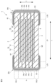
- 2 is a cross-sectional view taken along line II in FIG. 1.
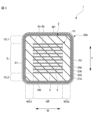
- 2 is a cross-sectional view taken along line II-II of FIG. 1.
- FIG. 2 is an enlarged view of the frame R1 in FIG.
- FIG. 5 is an enlarged view of the frame R2 in FIG. 4 .
- FIG. 2 is a diagram showing an example of a Ni-coated filler.
- FIG. 2 is a diagram showing an example of a Ni-coated filler.
- FIG. 2 is a diagram showing an example of a Ni-coated filler.
- FIG. 2 is a diagram showing an example of a Ni-coated filler.
- FIG. 2 is a diagram showing an example of a Ni-coated filler.
- FIG. 1 is a diagram showing characteristics of an example and a comparative example.
- Fig. 1 is a perspective view of a multilayer ceramic capacitor 1 according to an embodiment of the present invention.
- the laminate 2 includes a plurality of dielectric layers and a plurality of internal electrode layers that are stacked.
- the shape of the laminate 2 is approximately a rectangular parallelepiped.
- the direction in which the dielectric layers and the internal electrode layers are stacked is defined as a height direction T.
- the direction perpendicular to the height direction T is defined as a width direction W.
- the direction perpendicular to the height direction T and the width direction W is defined as a length direction L.
- one of the two faces that face each other in the height direction T is the first main surface M1.
- the remaining face is the second main surface M2.
- one of the two faces that face each other in the width direction W is the first side surface S1.
- the remaining face is the second side surface.
- one of the two faces that face each other in the length direction L is the first end surface E1.
- the remaining face is the second end surface E2.
- the mounting surface of the multilayer ceramic capacitor 1 is the second main surface M2.
- the mounting surface refers to the surface that faces a wiring board or the like when the multilayer ceramic capacitor 1 is mounted on a wiring board or the like.
- the cross section taken along line I-I in FIG. 1 is taken as the LT cross section.
- the cross section taken along line II-II in FIG. 1 is taken as the WT cross section.
- intersection of three faces of the laminate 2 is the corner of the laminate 2, and the intersection of two faces of the laminate 2 is the ridge of the laminate 2. It is preferable that the corners and ridges are rounded.
- the total number of dielectric layers laminated in the laminate 2 is preferably 15 or more and 2000 or less.
- the main material of the dielectric layers is a ceramic material. Examples of the ceramic material are dielectric ceramics containing BaTiO 3 , CaTiO 3 , SrTiO 3 , CaZrO 3 or the like as main components.
- the ceramic material may be a dielectric ceramic containing these main components and additional components such as Mn compounds, Fe compounds, Cr compounds, Co compounds, Ni compounds or the like.
- each dielectric layer is preferably 0.5 ⁇ m or more and 10 ⁇ m or less.
- Fig. 2 is a cross-sectional view taken along line II in Fig. 1.
- the laminate 2 can be divided into a first main surface side outer layer portion OL1, an inner layer range IL, and a second main surface side outer layer portion OL2 in the height direction T.
- the first main surface side outer layer portion OL1, the inner layer range IL, and the second main surface side outer layer portion OL2 are arranged in this order from the first main surface M1 to the second main surface M2 in the height direction T.
- the first main surface side outer layer portion OL1 is the portion between the internal electrode layer closest to the first main surface M1 and the first main surface M1.
- the internal layer range IL is the range where the internal electrode layers face each other.
- the second main surface side outer layer portion OL2 is the portion between the internal electrode layer closest to the second main surface M2 and the second main surface M2.
- the first main surface side outer layer portion OL1 is located on the first main surface M1 side of the laminate 2.
- the first main surface side outer layer portion OL1 is formed by an assembly of multiple dielectric layers located between the first main surface M1 and the internal electrode layer closest to the first main surface M1.
- the first main surface side outer layer portion OL1 is formed by multiple dielectric layers located between the first main surface M1 and the outermost surface of the inner layer range IL on the first main surface M1 side and an extension of that outermost surface.
- the second main surface side outer layer portion OL2 is located on the second main surface M2 side of the laminate 2.
- the second main surface side outer layer portion OL2 is formed by an assembly of multiple dielectric layers located between the second main surface M2 and the internal electrode layer closest to the second main surface M2.
- the second main surface side outer layer portion OL2 is formed by multiple dielectric layers located between the second main surface M2 and the outermost surface of the inner layer range IL on the second main surface M2 side and an extension of that outermost surface.
- the inner layer range IL is the range sandwiched between the first main surface side outer layer portion OL1 and the second main surface side outer layer portion OL2.
- the dielectric layers disposed in the first main surface side outer layer portion OL1 and the second main surface side outer layer portion OL2 are referred to as outer dielectric layer 3.
- the dielectric layers disposed in the inner layer range IL are referred to as inner dielectric layer 4.
- the length in the length direction L is the lengthwise length.
- the length in the width direction W is the widthwise length.
- the length in the height direction T is the heightwise length.
- the position that is half the length in the longitudinal direction is the center position in the longitudinal direction L.
- the center position in the longitudinal direction L is the center position in the longitudinal direction.
- the position that is half the widthwise length is the center position in the width direction W.
- the center position in the width direction W is the widthwise center position.
- the position that is half the length in the height direction is the center position in the height direction T.
- the center position in the height direction T is the center position in the height direction.
- the end in the length direction L is the length direction end.
- the end in the width direction W is the width direction end.
- the end in the height direction T is the height direction end.
- the size of the laminate 2 is not particularly limited.
- the length of the laminate in the longitudinal direction is preferably 0.2 mm or more and 10 mm or less.
- the length of the laminate 2 in the width direction is preferably 0.1 mm or more and 5 mm or less.
- the length of the laminate 2 in the height direction is preferably 0.1 mm or more and 5 mm or less.
- the laminate 2 can be divided into a first end surface side outer layer portion LG1, a longitudinally facing portion LF, and a second end surface side outer layer portion LG2 in the longitudinal direction L.
- the first end surface side outer layer portion LG1, the longitudinally facing portion LF, and the second end surface side outer layer portion LG2 are arranged in this order in the longitudinal direction L from the first end surface E1 to the second end surface E2.
- the longitudinal opposing portion LF is a portion where the internal electrode layers face each other in the height direction T.
- the first end face side outer layer portion LG1 is a portion between the longitudinal opposing portion LF and the first end face E1.
- the second end face side outer layer portion LG2 is a portion between the longitudinal opposing portion LF and the second end face E2.
- the longitudinal opposing portion LF is a portion that corresponds to the opposing electrode portion of the internal electrode layer.
- the first end face side outer layer portion LG1 and the second end face side outer layer portion LG2 are portions that correspond to the lead-out electrode portion of the internal electrode layer.
- the first end face side outer layer portion LG1 and the second end face side outer layer portion LG2 are also called L gaps.
- the opposing electrode portion includes a first opposing electrode portion 7a and a second opposing electrode portion 7b.
- the extraction electrode portion includes a first extraction electrode portion 8a and a second extraction electrode portion 8b. The opposing electrode portion and the extraction electrode portion will be described later.
- the first end face side outer layer portion LG1 is located on the first end face E1 side.
- the first end face side outer layer portion LG1 is located between the first end face E1 and the end of the second internal electrode layer 6b on the first end face E1 side.
- the second end face side outer layer portion LG2 is located on the second end face E2 side.
- the second end face side outer layer portion LG2 is located between the second end face E2 and the end of the first internal electrode layer 6a on the second end face E2 side.
- Fig. 3 is a cross-sectional view taken along line II-II in Fig. 1.
- the laminate 2 can be divided into a first side surface outer layer portion WG1, a widthwise opposing portion WF, and a second side surface outer layer portion WG2 in the width direction W.
- the first side surface outer layer portion WG1, the widthwise opposing portion WF, and the second side surface outer layer portion WG2 are arranged in this order in the width direction W from the first side surface S1 to the second side surface S2.
- the widthwise opposing portion WF is the portion where the internal electrode layers oppose each other in the height direction T.
- the first side surface side outer layer portion WG1 is the portion between the widthwise opposing portion WF and the first side surface S1.
- the second side surface side outer layer portion WG2 is the portion between the widthwise opposing portion WF and the second side surface S2.
- the first side surface side outer layer portion WG1 and the second side surface side outer layer portion WG2 are also called the W gap.
- the first side surface side outer layer portion WG1 and the second side surface side outer layer portion WG2 are portions where no internal electrode layer exists in the height direction T.
- the first side surface side outer layer portion WG1 is located on the first side surface S1 side.
- the first side surface side outer layer portion WG1 is formed by multiple dielectric layers located between the first side surface S1 and the outermost surface of the widthwise opposing portion WF on the first side surface S1 side.
- the second side surface outer layer portion WG2 is located on the second side surface S2 side.
- the second side surface outer layer portion WG2 is formed by multiple dielectric layers located between the second side surface S2 and the outermost surface of the widthwise opposing portion WF on the second side surface S2 side.
- the internal electrode layers include a plurality of first internal electrode layers 6a and a plurality of second internal electrode layers 6b.
- the first internal electrode layers 6a are internal electrode layers exposed at the first end face E1.
- the second internal electrode layers 6b are internal electrode layers exposed at the second end face E2.
- the first internal electrode layer 6a can be divided into a first opposing electrode portion 7a and a first extraction electrode portion 8a.
- the first opposing electrode portion 7a is the portion that faces the second internal electrode layer 6b.
- the first extraction electrode portion 8a is the portion that is extracted from the first opposing electrode portion 7a to the first end face E1 of the laminate 2.
- the end of the first extraction electrode portion 8a on the first end face E1 side is extended to the surface of the first end face E1 of the laminate 2.
- the end of the first extraction electrode portion 8a extended to the first end face E1 forms an exposed portion at the first end face E1.
- the second internal electrode layer 6b can be divided into a second opposing electrode portion 7b and a second extraction electrode portion 8b.
- the second opposing electrode portion 7b is the portion that faces the first internal electrode layer 6a.
- the second extraction electrode portion 8b is the portion that is extracted from the second opposing electrode portion 7b to the second end face E2 of the laminate 2.
- the end of the second extraction electrode portion 8b on the second end face E2 side is extended to the surface of the second end face E2 of the laminate 2.
- the end of the second extraction electrode portion 8b extended to the second end face E2 forms an exposed portion at the second end face E2.
- the shapes of the first opposing electrode portion 7a and the second opposing electrode portion 7b are not particularly limited.
- the shapes of the first opposing electrode portion 7a and the second opposing electrode portion 7b are preferably rectangular.
- the corners of the first opposing electrode portion 7a and the corners of the second opposing electrode portion 7b may be rounded.
- the corners of the first opposing electrode portion 7a and the corners of the second opposing electrode portion 7b may be formed at an angle. Forming at an angle means forming them in a tapered shape.
- the shapes of the first and second extraction electrodes 8a and 8b are not particularly limited.
- the shapes of the first and second extraction electrodes 8a and 8b are preferably rectangular.
- the corners of the first and second extraction electrodes 8a and 8b may be rounded.
- the corners of the first and second extraction electrodes 8a and 8b may be formed at an angle. Forming at an angle means forming them in a tapered shape.
- the width of the first opposing electrode portion 7a and the width of the first extension electrode portion 8a may be the same. Either one of the width of the first opposing electrode portion 7a and the width of the first extension electrode portion 8a may be narrower than the remaining one.
- the width of the second opposing electrode portion 7b and the width of the second extension electrode portion 8b may be the same. Either one of the width of the second opposing electrode portion 7b and the width of the second extension electrode portion 8b may be narrower than the remaining one.
- the material of the first internal electrode layer 6a and the second internal electrode layer 6b can be, for example, a metal such as Ni, Cu, Ag, Pd, or Au.
- the material of the first internal electrode layer 6a and the second internal electrode layer 6b can be an alloy containing at least one of the aforementioned metals, such as an Ag-Pd alloy.
- the first opposing electrode portion 7a and the second opposing electrode portion 7b face each other via the inner dielectric layer 4, forming a capacitance. This allows the multilayer ceramic capacitor 1 to exhibit the characteristics of a capacitor.
- the thickness of the first internal electrode layer 6a and the second internal electrode layer 6b is preferably, for example, about 0.2 ⁇ m or more and 2.0 ⁇ m or less.
- the total number of the first internal electrode layers 6a and the second internal electrode layers 6b is preferably 15 or more and 2000 or less.
- the portion where the first internal electrode layer 6a and the second internal electrode layer 6b face each other is defined as an inner layer portion 10.
- the inner layer portion 10 is a portion where the lengthwise facing portion LF shown in FIG. 2 and the widthwise facing portion WF shown in FIG. 3 intersect with the inner layer range IL.
- the shape of the inner layer portion 10 is approximately a rectangular parallelepiped.
- the portion where the lengthwise facing portion LF and the inner layer range IL intersect is shown as the inner layer portion 10.
- the portion where the widthwise facing portion WF and the inner layer range IL intersect is shown as the inner layer portion 10.
- the external electrodes include a first external electrode 20a and a second external electrode 20b.
- the first external electrode 20a is an external electrode connected to the first internal electrode layer 6a.
- the first external electrode 20a is disposed on the first end face E1, a portion of the first main surface M1, a portion of the second main surface M2, a portion of the first side surface S1, and a portion of the second side surface S2.
- the second external electrode 20b is an external electrode connected to the second internal electrode layer 6b.
- the second external electrode 20b is disposed on the second end face E2, a portion of the first main surface M1, a portion of the second main surface M2, a portion of the first side surface S1, and a portion of the second side surface S2.
- the external electrode preferably includes a base electrode layer, a conductive resin layer, and a plating layer.
- the plating layer preferably includes a Ni plating layer and a Sn plating layer.
- an external electrode including a base electrode layer, a conductive resin layer, a Ni plating layer, and a Sn plating layer is described.
- the base electrode layer includes a first base electrode layer 21a and a second base electrode layer 21b.
- the first base electrode layer 21a is disposed on the first end face E1, a part of the first main surface M1, a part of the second main surface M2, a part of the first side surface S1, and a part of the second side surface S2.
- the second base electrode layer 21b is disposed on the second end face E2, a part of the first main surface M1, a part of the second main surface M2, a part of the first side surface S1, and a part of the second side surface S2.
- the base electrode layer contains a conductive metal and a glass component.
- the conductive metal is at least one of Cu, Ni, Ag, Pd, Ag-Pd alloy, Au, etc.
- the glass component is at least one of B, Si, Ba, Mg, Al, Li, etc.
- the base electrode layer may be formed in multiple layers.
- the base electrode layer may be formed by applying a conductive paste containing a glass component and a metal to the laminate and then firing the laminate.
- the base electrode layer may be fired simultaneously with the firing of the internal electrode layer. Alternatively, the base electrode layer may be fired separately after the firing of the internal electrode layer.
- the base electrode layer When the base electrode layer is fired simultaneously with the internal electrode layer, it is preferable to add a dielectric material to the conductive paste instead of the glass component. This can improve the adhesion between the base electrode layer and the laminate 2.
- the thickness of the base electrode layer located on the first end face E1 or the first end face E2 at the center position in the height direction is preferably 10 ⁇ m or more and 150 ⁇ m or less.
- the thickness of the base electrode layer at the center position in the longitudinal direction on the first main surface M1, the second main surface M2, the first side surface S1, and the second side surface S2 is 5 ⁇ m or more and 50 ⁇ m or less.
- the base electrode layer can also be a thin film layer.
- the thin film layer can be formed by a thin film formation method such as a sputtering method or a vapor deposition method.
- the formed thin film layer is a layer in which metal particles are deposited.
- the thickness of the thin film layer is preferably 1 ⁇ m or less.
- a conductive resin layer is disposed on the base electrode layer.
- the conductive resin layer includes a resin component and a metal component.
- the conductive resin layer includes a first conductive resin layer 22 a and a second conductive resin layer 22 b.
- the first conductive resin layer 22a is disposed on the first underlying electrode layer 21a.
- the first conductive resin layer 22a covers the first underlying electrode layer 21a.
- the second conductive resin layer 22b is disposed on the second underlying electrode layer 21b.
- the second conductive resin layer 22b covers the second underlying electrode layer 21b. It is preferable that the ends of the conductive resin layers are in contact with the laminate 2.
- the conductive resin layer contains a thermosetting resin. By containing a thermosetting resin, the conductive resin layer is more flexible than the underlying electrode layer.
- the conductive resin layer functions as a buffer layer. Therefore, when a bending stress is applied to the mounting board and this stress applies a physical impact to the multilayer ceramic capacitor 1, cracks are unlikely to occur in the multilayer ceramic capacitor 1. When a shock caused by a thermal cycle is applied to the multilayer ceramic capacitor 1, cracks are unlikely to occur in the multilayer ceramic capacitor 1.
- the thermosetting resin contained in the conductive resin layer can be a thermosetting resin such as epoxy resin, phenol resin, urethane resin, silicone resin, or polyimide resin.
- epoxy resin is one of the most suitable resins.
- Epoxy resin has excellent heat resistance, moisture resistance, and adhesion.
- the conductive resin layer preferably contains a curing agent in addition to the thermosetting resin.
- the curing agent can be a compound such as a phenol-based, amine-based, acid anhydride-based, imidazole-based, active ester-based, or amide-imide-based compound.
- the conductive resin layer contains a metal component.
- the inclusion of the metal component in the conductive resin layer makes the conductive resin layer conductive.
- the metal component contained in the conductive resin layer is contained in the conductive resin layer as a metal filler. Contact between the metal fillers forms a conductive path inside the conductive resin layer.
- the conductive resin layer becomes conductive due to the formed conductive path.
- the metal component will be explained later.
- the thickness of the conductive resin layer 22 located on the first end face E1 or the second end face E2 at the center position in the height direction is preferably 10 ⁇ m or more and 200 ⁇ m or less.
- the thickness of the conductive resin layer at the center position in the longitudinal direction on the first main surface M1, the second main surface M2, the first side surface S1, and the second side surface S2 is 10 ⁇ m or more and 200 ⁇ m or less.
- the plating layer includes a Ni plating layer and a Sn plating layer.
- Ni plating layer The Ni plating layer is disposed on the conductive resin layer.
- the Ni plating layer covers at least a portion of the conductive resin layer.
- the Ni plating layer includes a first Ni plating layer 23a and a second Ni plating layer 23b.
- the first Ni plating layer 23a is disposed on the first conductive resin layer 22a.
- the second Ni plating layer 23b is disposed on the second conductive resin layer 22b.
- the Ni plating layer prevents the underlying electrode layer and other layers from being eroded by solder when mounting the multilayer ceramic capacitor 1.
- the Sn plating layer is disposed on the Ni plating layer.
- the Sn plating layer covers at least a portion of the Ni plating layer.
- the Sn plating layer includes a first Sn plating layer 24a and a second Sn plating layer 24b.
- the first Sn plating layer 24a is disposed on the first Ni plating layer 23a.
- the second Sn plating layer 24b is disposed on the second Ni plating layer 23b.
- the Sn plating layer has good solder wettability.
- the Sn plating layer makes it easy to mount the multilayer ceramic capacitor 1 on a substrate, etc.
- each Ni plating layer and Sn plating layer is preferably 2 ⁇ m or more and 15 ⁇ m or less.
- the size of the multilayer ceramic capacitor 1 is not particularly limited.
- the preferred length of the multilayer ceramic capacitor 1 including the laminate 2 and the external electrodes is 0.2 mm or more and 10 mm or less.
- the preferred height of the multilayer ceramic capacitor 1 including the laminate 2 and the external electrodes is 0.1 mm or more and 5 mm or less.
- the preferred width of the multilayer ceramic capacitor 1 including the laminate 2 and the external electrodes is 0.1 mm or more and 10 mm or less.
- the metal component contained in the conductive resin layer contains a metal component to impart conductivity to the conductive resin layer.
- the metal component contained in the conductive resin layer can be Ag, Cu, Ni, Sn, Bi, or an alloy containing any of these. It is particularly preferable that the metal component contains Ag. Ag may be simple Ag. Or, Ag may be an alloy containing Ag.
- Figure 4 is an enlarged view of the enclosed area R1 in Figure 1.
- the conductive resin layer will be described using the second conductive resin layer 22b as an example. However, what is described below also applies to the first conductive resin layer 22a.
- metal filler 30 is disposed in second conductive resin layer 22b. Metal filler 30 is disposed and dispersed in conductive resin 38.
- the shape of the metal filler 30 contained in the conductive resin layer is not particularly limited.
- the shape of the metal filler 30 may be spherical or flat.
- the metal filler 30 may be a mixture of spherical metal powder and flat metal powder.
- FIG. 4 shows an example of a metal filler 30 that has a flat shape.
- the average particle size of the metal filler 30 contained in the conductive resin layer is not particularly limited.
- the average particle size of the metal filler 30 can be, for example, 0.1 ⁇ m or more and 1 ⁇ m or less.
- the average particle size of the metal filler contained in the conductive resin layer can be calculated using a laser diffraction particle size measurement method (based on IOS 13320). This method of calculating the average particle size can be applied regardless of the shape of the filler.
- the amount of resin contained in the conductive resin layer is preferably 25 vmol% or more and 65 vmol% or less relative to the total volume of the conductive resin layer.
- the amount of metal components contained in the conductive resin layer is preferably 35 vmol% or more and 75 vmol% or less relative to the total volume of the conductive resin layer.
- Ni is disposed on at least a part of the surface of the metal filler 30.
- Fig. 5A is an enlarged view of the frame R2 in Fig. 4.
- the Ni disposed on the surface of the metal filler 30 is referred to as Ni portion 32.
- the Ni portion 32 is disposed on the entire surface of the metal filler 30.
- Sn may further be disposed on at least a part of the surface of the metal filler 30 or at least a part of the outer surface of the Ni portion 32.
- the Sn disposed on the surface of the metal filler 30 is referred to as Sn portion 34.
- the Sn portion 34 is disposed on a part of the outer surface of the Ni portion 32.
- Ni portion 32 and Sn portion 34 are disposed on the surface of metal filler 30.
- the Ni portion 32 is disposed on the entire outer periphery of the metal filler 30.
- the Ni portion 32 does not need to be disposed on the entire outer periphery of the metal filler 30, and it is sufficient that the Ni portion 32 is disposed on at least a portion of the outer periphery.
- the Sn portion 34 is disposed on the outer surface of the Ni portion 32.
- the Sn portion 34 does not have to be disposed on the outer surface of the Ni portion 32, and may be disposed on the surface of the metal filler 30.
- the Sn portion 34 may be disposed on the outer surface of the Ni portion 32 and on the surface of the metal filler 30.
- the Ni portion 32 disposed on the surface of the metal filler 30 is formed from Ni, which is a component of the Ni plating layer.
- Ni which is a component of the Ni plating layer, refers to the Ni material used when forming the Ni plating layer. In this case, the Ni portion 32 is formed at the same time as forming the Ni plating layer.
- the Ni portion 32 is made of Ni, which is a component of the Ni plating layer, it is possible to increase the electrical connection between the resin electrode layer and the plating layer. Furthermore, by having the Sn portion 34, it is possible to further increase the electrical connection between the resin electrode layer and the plating layer.
- the metal filler 30 of this embodiment at least a portion of the surface of the metal filler 30 is coated with the Ni portion 32.
- the metal filler 30 in which at least a portion of the surface of the metal filler 30 is coated with the Ni portion 32 is referred to as a Ni-coated filler 36.
- FIGS. 5B to 5F are diagrams showing examples of the Ni-coated filler 36.
- the Ni-coated filler 36 may have a form as shown in FIGS. 5B to 5F.
- the entire surface of the metal filler 30 is covered with the Ni portion 32. More specifically, the entire surface of the metal filler 30 is covered only with the Ni portion 32.
- FIG. 5B the entire surface of the metal filler 30 is covered with the Ni portion 32. More specifically, the entire surface of the metal filler 30 is covered only with the Ni portion 32.
- the entire surface of the metal filler 30 is covered with the Ni portion 32, and further, the Sn portion 34 is disposed on at least a portion of the outer surface of the Ni portion 32. More specifically, the Sn portion 34 is disposed only on a portion of the outer surface of the Ni portion 32.
- the entire surface of the metal filler 30 is covered with the Ni portion 32, and the entire outer surface of the Ni portion 32 is covered with the Sn portion 34.
- the Ni portion 32 is disposed on a portion of the surface of the metal filler 30, and the entire outer surface of the Ni portion 32 is covered with the Sn portion 34.
- FIG. 5C the entire surface of the metal filler 30 is covered with the Ni portion 32, and further, the Sn portion 34 is disposed on at least a portion of the outer surface of the Ni portion 32. More specifically, the Sn portion 34 is disposed only on a portion of the outer surface of the Ni portion 32.
- the entire surface of the metal filler 30 is covered with the Ni portion 32, and the entire outer surface of the Ni portion 32
- the Ni portion 32 is disposed on a portion of the surface of the metal filler 30, and the Sn portion 34 is disposed on another portion of the surface of the metal filler 30.
- the Sn portion 34 may be disposed on at least a portion of the surface of the metal filler 30, or at least a portion of the outer surface of the Ni portion 32.
- the entire surface of the metal filler 30 may be covered with the Ni portion 32 or the Sn portion 34.
- a portion of the surface of the metal filler 30 may be covered with the Ni portion 32, and the remaining other surface may be covered with the Sn portion 34.
- the metal filler 30 of this embodiment only needs to have the Ni portion 32 disposed on at least a portion of the surface of the metal filler 30.
- Ni-coated filler layer In the resin electrode layer, a layer in which the Ni-coated filler 36 exists is defined as a Ni-coated filler layer. In the example shown in Fig. 5A, a range belonging to the same position as the position in the height direction T in which the Ni-coated filler 36 exists is the Ni-coated filler layer.
- Ni portions 32, and more preferably Sn portions 34, in the metal filler 30 it is possible to reduce the ESR (Equivalent Series Resistance).
- Ni contained in Ni portion 32 is Ni, which is a component of the Ni plating layer, and preferably Sn portion 34 is also disposed, which increases the electrical connection between the resin electrode layer and the plating layer.
- FIG. 5A illustrates a state in which the Ni portion 32 arranged on the metal filler 30 is in contact with the second plating layer 23b.
- FIG. 5A also illustrates a state in which the Sn portion 34 of the metal filler 30 is not in contact with other metal fillers 30.
- the portion where the metal filler 30 contacts the metal filler 30 may not be observed depending on the cross section observed. In other words, by changing the cross section observed, the portion where the metal filler 30 contacts the metal filler 30 can be observed.
- the metal filler 30 contacts the other metal fillers 30, thereby increasing the conductivity of the resin electrode layer.
- the area in which the Ni-coated filler layer is disposed is preferably located within a range of 5.0 ⁇ m or less from the interface between the conductive resin layer and the Ni plating layer toward the inside of the laminate 2 in the height direction T.
- the area in which the Ni-coated filler layer is disposed is preferably located within a range of 5.0 ⁇ m or less from the interface between the conductive resin layer and the Ni plating layer toward the inside of the laminate 2 in the depth direction.
- the area in which the Ni-coated filler layer is disposed is disposed within a range of 0.5 ⁇ m or more and 5.0 ⁇ m or less from the interface between the conductive resin layer and the Ni plating layer toward the inside of the laminate 2 in the height direction T.
- the area in which the Ni-coated filler layer is disposed refers to the range in the height direction T at the position where the Ni-coated filler layer is disposed.
- Line A in FIG. 4 is a line showing the interface between the second conductive resin layer 22b and the second Ni plating layer 23b.
- Arrow B in FIG. 4 is an arrow showing the direction from the interface A between the second conductive resin layer 22b and the second Ni plating layer 23b toward the inside of the laminate 2 in the height direction T.
- the Ni-coated filler layer is disposed within a range of 5.0 ⁇ m or less in the direction B toward the inside of the laminate 2 from the interface A between the second conductive resin layer 22b and the second Ni plating layer 23b, making it possible to obtain the effect of reducing ESR while ensuring the mechanical strength of the laminated ceramic capacitor.
- the electrical coupling between the second conductive resin layer 22b and the second Ni plating layer 23b or the second Sn plating layer 24b can be further increased, and the ESR can be further reduced.
- FIG. 6 shows an example of this embodiment and a comparative example.
- the presence depth shown in FIG. 6 is the depth at which the Ni-coated filler 36 exists, and is the distance from the interface A between the conductive resin layer and the Ni plating layer of the Ni-coated filler layer in the direction B toward the inside of the laminate 2.
- the conditions for the multilayer ceramic capacitor used in the evaluation are as follows.
- the size of the multilayer ceramic capacitor is 3.2 mm in length, 1.6 mm in width, and 1.6 mm in height.
- the capacitance of the multilayer ceramic capacitor is 0.01 ⁇ F.
- the rated voltage of the multilayer ceramic capacitor is 630 V.
- the ESR measurement method and criteria are as follows. Before measuring the ESR, the multilayer ceramic capacitor was heat-treated in an air atmosphere at 150°C for 1 hour, then mounted on a measurement board, and 24 ⁇ 2 hours after the heat treatment was completed, the measurement was performed using a network analyzer at a measurement frequency of 1 MHz.
- the ESR value shown in Figure 6 is the average value of 100 ESR measurements.
- the average of the 100 ESR measurements was 250 m ⁇ or less, it was marked as ⁇ , if it was between 250 m ⁇ and 300 m ⁇ , it was marked as ⁇ , and if it was greater than 300 m ⁇ , it was marked as ⁇ .
- the evaluation method and criteria for mechanical strength are as follows. Mechanical strength was evaluated based on the resistance to cracking. The mechanical strength was evaluated by performing a deflection test using the JIS C 6484 method on 30 plated multilayer ceramic capacitors, and the number of cracks that occurred when the deflection was fixed at 5 mm was measured.
- the overall evaluation is the result of a comprehensive assessment based on the ESR value and the state of crack occurrence. Good is indicated by a circle, no particular problems by a triangle, and problems by an x.
- the comparative multilayer ceramic capacitor does not have a Ni-coated filler layer.
- the comparative multilayer ceramic capacitor has an ESR rating of x and an overall rating of x.
- a Ni-coated filler layer is disposed to a predetermined depth.
- the ESR was judged as ⁇ .
- the ESR was judged as ⁇ . Note that when the depth is 0.4 ⁇ m or less, the bonding area between the fillers via the Ni portion and the bonding area between the filler and the plating layer decreases, which is thought to increase the electrical loss and the ESR.
- the overall evaluation was rated as ⁇ .
- the LT cross section shown in Fig. 4 can be observed, for example, as follows.
- the multilayer ceramic capacitor 1 is polished to the center position in the width direction.
- the cross section exposed by polishing is then observed with an optical microscope or the like.
- the length and thickness of each part can be measured from the observed cross section.
- the conductive paste for the dielectric sheet and the internal electrode layer contains a binder and a solvent.
- the binder and the solvent may be a known organic binder and an organic solvent, etc.
- a conductive paste for the internal electrode layer is printed in a predetermined pattern on the dielectric sheet.
- the internal electrode layer pattern is formed by printing the conductive paste.
- the printing can be performed by, for example, screen printing or gravure printing.
- a predetermined number of dielectric sheets for the outer layer are stacked. No internal electrode layer pattern is printed on the dielectric sheets for the outer layer. Dielectric sheets with internal electrode layer patterns printed on them are stacked in order on top of the stacked dielectric sheets. A predetermined number of dielectric sheets for the outer layer are then stacked on top of them. A laminated sheet is produced by stacking these layers.
- the laminated sheet is pressed in the height direction to produce a laminated block.
- the pressing method can be a hydrostatic press.
- the laminated block is cut to a predetermined size. This cutting process cuts out laminated chips. When cutting, the corners and edges of the laminated chips may be rounded. Barrel polishing may be used to round them.
- the laminated chip is fired. This firing produces a laminate.
- the preferred firing temperature is 900°C or higher and 1200°C or lower. The firing temperature can be changed depending on the materials of the dielectric and internal electrode layers.
- the laminate is provided with external electrodes.
- a conductive paste that will become the base electrodes is applied to both end surfaces of the laminate.
- the conductive paste contains a glass component and a metal.
- the application method can be, for example, a dipping method.
- a firing process is performed.
- a base electrode layer is formed by this firing process.
- the preferred temperature for the firing process is 700° C. or higher and 900° C. or lower.
- the base electrode layer is a fired layer.
- the conductive resin layer is formed on the base electrode layer.
- a conductive resin paste is prepared.
- the conductive resin paste contains a resin component and a metal filler.
- the conductive resin paste is applied onto the base electrode layer.
- the application method can be a dipping method.
- the solvent for the conductive resin paste is diethylene glycol monobutyl ether (molecular weight 162.23, boiling point 230° C.) to which is added a high boiling point solvent having a boiling point of 250° C. or higher, as shown below.
- Dibutyl sebacate (molecular weight 314.47, boiling point 345°C) Diethyl sebacate (molecular weight 258.36, boiling point 309°C) Dibutyl adipate (molecular weight 258.36, boiling point 305°C) Dimethyl sebacate (molecular weight 230.30, boiling point 294°C) Diethyl suberate (molecular weight 230.30, boiling point 283°C) Dibutyl succinate (molecular weight 230.30, boiling point 274°C) Diethyl adipate (molecular weight 202.25, boiling point 251°C)
- dibutyl adipate (molecular weight 258.36, boiling point 305°C) is used.
- the heat treatment involves drying in a hot air oven at 150°C to 180°C for 10 minutes. After that, the material is cured in an air atmosphere at 200°C to 280°C for 60 minutes. This heat curing forms a conductive electrode layer.
- Ni from the Ni plating which will be explained later, flows into these voids, forming Ni-coated filler and ultimately a Ni-coated filler layer.
- the atmosphere during the heat treatment is preferably a nitrogen gas atmosphere.
- the preferred oxygen concentration is 100 ppm or less. This oxygen concentration makes it difficult for the resin to scatter. In addition, this oxygen concentration makes it difficult for various metal components to oxidize.
- Ni plating layer is formed on the surface of the conductive resin layer.
- This Ni plating layer becomes a first Ni plating layer and a second Ni plating layer.
- the method for forming the Ni plating layer may be an electrolytic plating method, and a preferred plating method is barrel plating.
- a Sn plating layer is formed on the Ni plating layer.
- a first Sn plating layer is formed on the first Ni plating layer.
- a second Sn plating layer is formed on the second Ni plating layer.
- Ni plating components flow into the gaps near the metal filler.
- the area in which the Ni-coated filler layer is formed can be controlled by controlling the current during Ni plating.
- Sn portions are to be placed on the surface of the metal filler in addition to Ni portions, Sn media may be mixed in during Ni plating using a barrel. This causes Ni portions to be placed on the surface of the metal filler, as well as Sn portions.
- the method of placing the Sn portions is not limited to this.
Landscapes
- Engineering & Computer Science (AREA)
- Power Engineering (AREA)
- Manufacturing & Machinery (AREA)
- Microelectronics & Electronic Packaging (AREA)
- Chemical & Material Sciences (AREA)
- Materials Engineering (AREA)
- Fixed Capacitors And Capacitor Manufacturing Machines (AREA)
- Ceramic Capacitors (AREA)
Priority Applications (5)
| Application Number | Priority Date | Filing Date | Title |
|---|---|---|---|
| CN202480021008.8A CN120836069A (zh) | 2023-03-29 | 2024-02-16 | 层叠陶瓷电容器 |
| KR1020257026920A KR20250136360A (ko) | 2023-03-29 | 2024-02-16 | 적층 세라믹 콘덴서 |
| EP24778811.0A EP4651164A1 (en) | 2023-03-29 | 2024-02-16 | Multilayer ceramic capacitor |
| JP2025509905A JPWO2024202666A1 (https=) | 2023-03-29 | 2024-02-16 | |
| US19/297,045 US20250364184A1 (en) | 2023-03-29 | 2025-08-12 | Multilayer ceramic capacitor |
Applications Claiming Priority (2)
| Application Number | Priority Date | Filing Date | Title |
|---|---|---|---|
| JP2023054073 | 2023-03-29 | ||
| JP2023-054073 | 2023-03-29 |
Related Child Applications (1)
| Application Number | Title | Priority Date | Filing Date |
|---|---|---|---|
| US19/297,045 Continuation US20250364184A1 (en) | 2023-03-29 | 2025-08-12 | Multilayer ceramic capacitor |
Publications (1)
| Publication Number | Publication Date |
|---|---|
| WO2024202666A1 true WO2024202666A1 (ja) | 2024-10-03 |
Family
ID=92904227
Family Applications (1)
| Application Number | Title | Priority Date | Filing Date |
|---|---|---|---|
| PCT/JP2024/005489 Ceased WO2024202666A1 (ja) | 2023-03-29 | 2024-02-16 | 積層セラミックコンデンサ |
Country Status (6)
| Country | Link |
|---|---|
| US (1) | US20250364184A1 (https=) |
| EP (1) | EP4651164A1 (https=) |
| JP (1) | JPWO2024202666A1 (https=) |
| KR (1) | KR20250136360A (https=) |
| CN (1) | CN120836069A (https=) |
| WO (1) | WO2024202666A1 (https=) |
Citations (3)
| Publication number | Priority date | Publication date | Assignee | Title |
|---|---|---|---|---|
| JPS5941489A (ja) * | 1982-08-31 | 1984-03-07 | C Uyemura & Co Ltd | 粉粒体への電気めつき方法 |
| JP2012104785A (ja) * | 2010-11-15 | 2012-05-31 | Tdk Corp | チップ型電子部品の実装構造、チップ型電子部品の実装方法、チップ型電子部品、及びチップ型電子部品の製造方法 |
| JP2014143387A (ja) * | 2013-01-24 | 2014-08-07 | Samsung Electro-Mechanics Co Ltd | 積層セラミックキャパシタ及びその製造方法 |
Family Cites Families (1)
| Publication number | Priority date | Publication date | Assignee | Title |
|---|---|---|---|---|
| JPH11162771A (ja) | 1997-11-25 | 1999-06-18 | Kyocera Corp | 積層セラミックコンデンサ |
-
2024
- 2024-02-16 KR KR1020257026920A patent/KR20250136360A/ko active Pending
- 2024-02-16 CN CN202480021008.8A patent/CN120836069A/zh active Pending
- 2024-02-16 JP JP2025509905A patent/JPWO2024202666A1/ja active Pending
- 2024-02-16 WO PCT/JP2024/005489 patent/WO2024202666A1/ja not_active Ceased
- 2024-02-16 EP EP24778811.0A patent/EP4651164A1/en active Pending
-
2025
- 2025-08-12 US US19/297,045 patent/US20250364184A1/en active Pending
Patent Citations (3)
| Publication number | Priority date | Publication date | Assignee | Title |
|---|---|---|---|---|
| JPS5941489A (ja) * | 1982-08-31 | 1984-03-07 | C Uyemura & Co Ltd | 粉粒体への電気めつき方法 |
| JP2012104785A (ja) * | 2010-11-15 | 2012-05-31 | Tdk Corp | チップ型電子部品の実装構造、チップ型電子部品の実装方法、チップ型電子部品、及びチップ型電子部品の製造方法 |
| JP2014143387A (ja) * | 2013-01-24 | 2014-08-07 | Samsung Electro-Mechanics Co Ltd | 積層セラミックキャパシタ及びその製造方法 |
Non-Patent Citations (1)
| Title |
|---|
| See also references of EP4651164A1 * |
Also Published As
| Publication number | Publication date |
|---|---|
| JPWO2024202666A1 (https=) | 2024-10-03 |
| KR20250136360A (ko) | 2025-09-16 |
| US20250364184A1 (en) | 2025-11-27 |
| CN120836069A (zh) | 2025-10-24 |
| EP4651164A1 (en) | 2025-11-19 |
Similar Documents
| Publication | Publication Date | Title |
|---|---|---|
| US10074483B2 (en) | Ceramic electronic component | |
| US11062848B2 (en) | Multilayer ceramic electronic component | |
| US10262799B2 (en) | Multilayer ceramic capacitor | |
| US11361906B2 (en) | Multilayer ceramic electronic component | |
| US10879004B2 (en) | Multilayer ceramic capacitor and multilayer ceramic capacitor-mounting structure | |
| JP7331622B2 (ja) | 積層セラミック電子部品 | |
| JP2021034458A (ja) | 積層セラミック電子部品 | |
| WO2023095620A1 (ja) | 積層セラミック電子部品 | |
| US11817266B2 (en) | Conductive paste and ceramic electronic component | |
| WO2024202666A1 (ja) | 積層セラミックコンデンサ | |
| CN120712623A (zh) | 层叠陶瓷电容器 | |
| WO2023243160A1 (ja) | 積層セラミックコンデンサ | |
| US20250372309A1 (en) | Multilayer ceramic capacitor | |
| US20260128229A1 (en) | Multilayer ceramic capacitor | |
| US20250054698A1 (en) | Multilayer ceramic electronic component | |
| JP2019179820A (ja) | 積層セラミックコンデンサ | |
| WO2025004487A1 (ja) | 積層セラミックコンデンサ | |
| WO2026054041A1 (ja) | 積層セラミックコンデンサ | |
| WO2025004486A1 (ja) | 積層セラミックコンデンサ | |
| WO2024247445A1 (ja) | 積層セラミックコンデンサ | |
| WO2025018006A1 (ja) | 積層セラミックコンデンサ | |
| JP2021166214A (ja) | 積層セラミックコンデンサおよびその製造方法 |
Legal Events
| Date | Code | Title | Description |
|---|---|---|---|
| 121 | Ep: the epo has been informed by wipo that ep was designated in this application |
Ref document number: 24778811 Country of ref document: EP Kind code of ref document: A1 |
|
| ENP | Entry into the national phase |
Ref document number: 1020257026920 Country of ref document: KR Free format text: ST27 STATUS EVENT CODE: A-0-1-A10-A15-NAP-PA0105 (AS PROVIDED BY THE NATIONAL OFFICE) |
|
| WWE | Wipo information: entry into national phase |
Ref document number: 1020257026920 Country of ref document: KR |
|
| ENP | Entry into the national phase |
Ref document number: 2025509905 Country of ref document: JP Kind code of ref document: A |
|
| WWE | Wipo information: entry into national phase |
Ref document number: 2025509905 Country of ref document: JP |
|
| WWE | Wipo information: entry into national phase |
Ref document number: 202517082961 Country of ref document: IN |
|
| WWP | Wipo information: published in national office |
Ref document number: 202517082961 Country of ref document: IN |
|
| WWE | Wipo information: entry into national phase |
Ref document number: 202480021008.8 Country of ref document: CN |
|
| WWP | Wipo information: published in national office |
Ref document number: 202480021008.8 Country of ref document: CN |
|
| NENP | Non-entry into the national phase |
Ref country code: DE |
|
| WWP | Wipo information: published in national office |
Ref document number: 2024778811 Country of ref document: EP |