WO2024201685A1 - 自発光型表示装置および自発光型表示装置の製造方法 - Google Patents
自発光型表示装置および自発光型表示装置の製造方法 Download PDFInfo
- Publication number
- WO2024201685A1 WO2024201685A1 PCT/JP2023/012359 JP2023012359W WO2024201685A1 WO 2024201685 A1 WO2024201685 A1 WO 2024201685A1 JP 2023012359 W JP2023012359 W JP 2023012359W WO 2024201685 A1 WO2024201685 A1 WO 2024201685A1
- Authority
- WO
- WIPO (PCT)
- Prior art keywords
- channel layer
- layer
- insulating layer
- display device
- self
- Prior art date
- Legal status (The legal status is an assumption and is not a legal conclusion. Google has not performed a legal analysis and makes no representation as to the accuracy of the status listed.)
- Ceased
Links
Images





Classifications
-
- G—PHYSICS
- G09—EDUCATION; CRYPTOGRAPHY; DISPLAY; ADVERTISING; SEALS
- G09F—DISPLAYING; ADVERTISING; SIGNS; LABELS OR NAME-PLATES; SEALS
- G09F9/00—Indicating arrangements for variable information in which the information is built-up on a support by selection or combination of individual elements
-
- G—PHYSICS
- G09—EDUCATION; CRYPTOGRAPHY; DISPLAY; ADVERTISING; SEALS
- G09F—DISPLAYING; ADVERTISING; SIGNS; LABELS OR NAME-PLATES; SEALS
- G09F9/00—Indicating arrangements for variable information in which the information is built-up on a support by selection or combination of individual elements
- G09F9/30—Indicating arrangements for variable information in which the information is built-up on a support by selection or combination of individual elements in which the desired character or characters are formed by combining individual elements
-
- H—ELECTRICITY
- H10—SEMICONDUCTOR DEVICES; ELECTRIC SOLID-STATE DEVICES NOT OTHERWISE PROVIDED FOR
- H10D—INORGANIC ELECTRIC SEMICONDUCTOR DEVICES
- H10D30/00—Field-effect transistors [FET]
- H10D30/01—Manufacture or treatment
- H10D30/021—Manufacture or treatment of FETs having insulated gates [IGFET]
-
- H—ELECTRICITY
- H10—SEMICONDUCTOR DEVICES; ELECTRIC SOLID-STATE DEVICES NOT OTHERWISE PROVIDED FOR
- H10D—INORGANIC ELECTRIC SEMICONDUCTOR DEVICES
- H10D30/00—Field-effect transistors [FET]
- H10D30/60—Insulated-gate field-effect transistors [IGFET]
- H10D30/67—Thin-film transistors [TFT]
Definitions
- This disclosure relates to a self-luminous display device and a method for manufacturing a self-luminous display device.
- Patent document 1 discloses that the thickness of the gate insulating film affects the threshold value of a transistor.
- the threshold value of a transistor is affected by the gate length and the carrier concentration in the channel layer. This means that the actual threshold value of the transistor varies, which can easily lead to a decrease in display quality.
- a self-luminous display device includes a first pixel circuit including a first transistor having a first channel layer including an oxide semiconductor, and a second pixel circuit having the same circuit configuration as the first pixel circuit, including a second transistor corresponding to the first transistor and having a second channel layer including an oxide semiconductor, the gate length of the second transistor being greater than the gate length of the first transistor, and the oxide semiconductor included in the second channel layer being more reduced than the oxide semiconductor included in the first channel layer.
- a method for manufacturing a self-luminous display device includes the steps of forming a channel layer including an oxide semiconductor of a transistor, forming a first insulating layer in contact with the channel layer, etching the first insulating layer with a first plasma to form a hole penetrating the first insulating layer or introducing oxygen into the first insulating layer, annealing the channel layer and the first insulating layer after the step using the first plasma, forming a conductor layer that will be the material of the gate electrode of the transistor, and etching the conductor layer with a second plasma to form the gate electrode of the transistor from the conductor layer.
- FIG. 1 is a plan view illustrating a configuration example of a self-luminous display device according to an embodiment of the present disclosure.
- 2 is a plan view perspective diagram showing a configuration example of a first transistor and a second transistor shown in FIG. 1 .
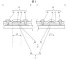
- 2 is a cross-sectional view showing a configuration example of a first transistor and a second transistor shown in FIG. 1 .
- 2 is a cross-sectional view showing a configuration example of a first transistor and a second transistor shown in FIG. 1 .
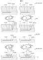
- 1A to 1C are cross-sectional views illustrating an example of a method for manufacturing a self-luminous display device according to an embodiment of the present disclosure.
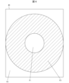
- FIG. 6 is a plan view showing an example of the intensity distribution of the plasma shown in FIG. 5 .
- 1 is a cross-sectional view showing a configuration example of a self-luminous display device according to an embodiment of the present disclosure.
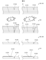
- 1A to 1C are cross-sectional views illustrating an example of a method for manufacturing a self-luminous display device according to an embodiment of the present disclosure.
- 1 is a cross-sectional view showing a configuration example of a self-luminous display device according to an embodiment of the present disclosure.
- 1A to 1C are cross-sectional views illustrating an example of a method for manufacturing a self-luminous display device according to an embodiment of the present disclosure.
- 1A to 1C are cross-sectional views illustrating an example of a method for manufacturing a self-luminous display device according to an embodiment of the present disclosure.
- FIG. 1 is a plan view showing an example of the configuration of a self-luminous display device according to an embodiment of the present disclosure.
- the self-luminous display device 1 includes a display unit DA including a plurality of pixels PX, and a drive circuit 10 that drives the display unit DA.
- Each of the plurality of pixels PX includes a light-emitting element 2 and a pixel circuit 3 that controls a current or voltage applied to the light-emitting element 2.
- Each of the pixel circuits 3 includes a transistor TX, and each of the transistors TX has a channel layer including an oxide semiconductor.
- the self-luminous display device 1 includes a first pixel circuit 31 including a first transistor T1 having a first channel layer including an oxide semiconductor, and a second pixel circuit 32 having the same circuit configuration as the first pixel circuit 31, corresponding to the first transistor T1, and including a second transistor T2 having a second channel layer including an oxide semiconductor. More specifically, the second pixel circuit 32 has the same circuit element arrangement and connection relationship as the first pixel circuit 31 in terms of design, and the characteristics of the corresponding circuit elements are the same. The characteristics of the circuit elements are, for example, the threshold value of the transistor and the capacitance value of the capacitance element.
- the threshold value of the gate voltage of a transistor using an oxide semiconductor depends on the gate length of the transistor and the degree of reduction of the oxide semiconductor in the transistor. Therefore, the first transistor T1 and the second transistor T2 have the same threshold value, gate length, and degree of reduction in terms of design.
- the first transistor T1 and the second transistor T2 may be drive transistors. Hereinafter, attention will be paid to the first transistor T1 and the second transistor T2.
- FIGS. 2, 3, and 4 are plan perspective, cross-sectional, and cross-sectional views showing configuration examples of the first and second transistors shown in FIG. 1.
- FIG. 3 shows the ABCD cross section of FIG. 2
- FIG. 4 shows the EFGHIJ cross section of FIG. 2.
- the first transistor T1 has a gate electrode G1, a source electrode S1, a drain electrode D1, and a first channel layer C1 including an oxide semiconductor.
- the second transistor T2 has a gate electrode G2, a source electrode S2, a drain electrode D2, and a second channel layer C2 including an oxide semiconductor.
- the actual gate length L2 of the second transistor T2 is greater than the actual gate length L1 of the first transistor T1, and the oxide semiconductor contained in the actual second channel layer C2 is more reduced than the oxide semiconductor contained in the actual first channel layer C1.
- the difference between the gate lengths L1 and L2 acts to make the threshold of the second transistor T2 larger than the threshold of the first transistor T1.
- the difference in the degree of reduction of the oxide semiconductor acts to make the threshold of the second transistor T2 smaller than the threshold of the first transistor T1.
- the difference in gate length directly leads to a difference in threshold value, and the difference in threshold value is large.
- a large difference in threshold value causes uneven brightness and deteriorates display quality.
- adjustments are usually made before shipping so that the uneven brightness is no longer visible (so-called "demura processing"), but there are cases where uneven brightness remains to a degree that is difficult to adjust.
- the difference in threshold value leads to differences in aging, causing uneven brightness after aging and deteriorating display quality.
- the difference in threshold value is small, and therefore the unevenness in raw luminance before the demurration process is small. This makes it possible to improve the display quality of the self-luminous display device 1, and in particular to improve the display quality after deterioration over time.
- the first transistor T1 and the second transistor T2 may each be a thin film transistor.
- the oxide semiconductor contained in the first channel layer C1 and the oxide semiconductor contained in the second channel layer C2 may be the same material.
- the oxide semiconductor may be, for example, copper oxide, silver oxide, zinc oxide, gallium oxide, tin oxide, indium oxide, indium gallium zinc oxide, indium tin oxide, indium zinc oxide, titanium oxide, indium titanium oxide, or indium titanium zinc oxide.
- the gate electrode G1 and the gate electrode G2 are formed from the same layer as each other, and the first channel layer C1 and the second channel layer C2 are formed from the same layer as each other.
- the source electrodes S1, S2 and the drain electrodes D1, D2 may each be formed from the same layer as each other.
- the self-luminous display device 1 includes a first insulating layer I1 having a first portion P1 in contact with the upper surface of the first channel layer C1 and a second portion P2 in contact with the upper surface of the second channel layer C2.
- the density of hydrogen contained in the second portion P2 is greater than the density of hydrogen contained in the first portion P1.
- the diameter of the second hole H2 penetrating the vicinity of the second portion P2 is smaller than the diameter of the first hole H1 penetrating the vicinity of the first portion P1.
- the first hole H1 is a through hole for dehydrogenating the first portion P1
- the second hole H2 is a through hole for dehydrogenating the second portion P2.
- the diameter of the second hole H2 may be 0, in other words, there may be no dehydrogenation hole in the vicinity of the second portion P2.
- the first insulating layer I1 may be an inorganic insulating layer and may include, for example, silicon nitride (SiN), silicon oxide (SiO), or silicon oxynitride (SiNO).
- (Production method) 5 is a cross-sectional view showing an example of a method for manufacturing a self-luminous display device according to an embodiment of the present disclosure.
- a first channel layer CX including an oxide semiconductor of a transistor is formed (step S10), and a first insulating layer I1 in contact with the channel layer CX is formed (step S20).
- the channel layer CX includes a first channel layer C1 and a second channel layer C2.
- the first insulating layer I1 is formed on the channel layer CX.
- the first insulating layer I1 contains hydrogen when it is formed.
- a photoresist layer 21 having an opening OX is formed on the first insulating layer I1 (step S22).
- the opening OX includes a first opening O1 overlapping the intended position of the first hole H1 and a second opening O2 overlapping the intended position of the second hole H2.
- the depth and diameter of the second opening O2 are the same as the depth and diameter of the first opening O1. It is beneficial that the opening OX does not penetrate through the substrate.
- the photoresist layer 21 having a non-penetrating opening OX can be realized using a halftone mask or a graytone mask.
- the photoresist layer 21 and the first insulating layer I1 are etched by the first plasma 41 so as to form holes HX penetrating the first insulating layer I1 (step S24), and the photoresist layer 21 is removed (step S26).
- the openings OX overlap with the holes HX in a plan view.
- the holes HX penetrating the first insulating layer I1 include a first hole H1 and a second hole H2.
- the stronger the first plasma 41 is the larger the diameters of the openings OX and holes HX become.
- the diameter of the first holes H1 formed in the area where the strength of the first plasma 41 is strong is larger than the diameter of the second holes H2 formed in the area where the strength of the first plasma 41 is weak.
- step S24 the photoresist layer 21 is etched by the first plasma 41 so that the opening OX penetrates the photoresist layer 21, and the first insulating layer I1 is further etched to form a hole HX.
- the diameter of the second hole H2 can be set to 0, in other words, a dehydrogenation hole is not formed in an area where the first plasma 41 is weak.
- the channel layer CX and the first insulating layer I1 are annealed (step S30).
- the annealing process liberates hydrogen from the first insulating layer I1, and some of the liberated hydrogen reduces the oxide semiconductor contained in the channel layer CX, while another part escapes without being reduced.
- the larger the diameter of the hole HX the easier it is for hydrogen to escape through the hole HX, and therefore the oxide semiconductor near the hole HX is not reduced as much.
- hydrogen liberated from the first portion P1 to the first channel layer C1 side is more likely to escape than hydrogen liberated from the second portion P2 to the second channel layer C2 side. Therefore, the oxide semiconductor contained in the second channel layer C2 is reduced more than the oxide semiconductor contained in the first channel layer C1.
- a conductor layer 13 that will be the material of the transistor gate electrode GX is formed (step S40), and a patterned template layer 51 is formed on the conductor layer 13 (step S42).
- the conductor layer 13 is etched by the second plasma 42 so as to form the transistor gate electrode GX from the conductor layer 13 (step S44), and the template layer 51 is removed.
- the gate electrode GX includes a gate electrode G1 and a gate electrode G2.
- This manufacturing method (at least partially) cancels out the effects of the gate length and the degree of reduction of the oxide semiconductor on the transistor threshold, thereby reducing the difference between the design threshold and the actual threshold of the transistor. It also reduces the difference in threshold between the first transistor T1 formed in an area with a strong plasma and the second transistor T2 formed in an area with a weak plasma.
- the first and second plasmas 41, 42 may each have a spatially non-uniform intensity distribution.
- the plasma is weak in the central region F1 and the outer peripheral region F2, and is strong in the intermediate region F3 therebetween.
- the shape of the intermediate region F3 corresponds to the shape of the plasma generating electrode and is usually annular. It is beneficial that the intensity distributions of the first and second plasmas 41, 42 are approximately the same as each other.
- the first and second plasmas 41, 42 are strong in the region where the first transistor T1 is formed, and the first and second plasmas 41, 42 are weak in the region where the second transistor T2 is formed.
- the intensity distribution may be measured, or the intensity distribution may be estimated from the configuration of the plasma generating device. If the shape and arrangement of the plasma generating electrodes are the same, it can be determined that the intensity distributions of the first and second plasmas 41, 42 are the same.
- the first and second plasmas 41 and 42 may also be generated by the same device.
- the self-luminous display device 1 includes a second insulating layer I2 having a third portion P3 in contact with the lower surface of the first channel layer C1 and a fourth portion P4 in contact with the lower surface of the second channel layer C2.
- the density of hydrogen contained in the fourth portion P4 is greater than the density of hydrogen contained in the third portion P3.
- the diameter of the fourth hole H4 penetrating the vicinity of the fourth portion P4 is smaller than the diameter of the third hole H3 penetrating the vicinity of the third portion P3.
- the third hole H3 is a through hole for dehydrogenating from the third portion P3, and the fourth hole H4 is a through hole for dehydrogenating from the fourth portion P4.
- the diameter of the fourth hole H4 may be 0, in other words, there may be no dehydrogenation hole in the vicinity of the fourth portion P4.
- the second insulating layer I2 may be an inorganic insulating layer and may contain, for example, silicon nitride (SiN), silicon oxide (SiO), or silicon oxynitride (SiNO).
- the third hole H3 may or may not overlap the first hole H1 in a planar view.
- the fourth hole H4 may or may not overlap the second hole H2 in a planar view.
- a second insulating layer I2 is formed on the opposite side of the first insulating layer I1 and in contact with the channel layer CX (step S50).
- the channel layer CX is to be formed on the second insulating layer
- the first insulating layer I1 is to be formed on the channel layer CX.
- the second insulating layer I2 also contains hydrogen when formed.
- a photoresist layer 22 having an opening OY is formed on the second insulating layer I2 (step S52).
- the opening OY includes a third opening O3 overlapping the planned position for forming the third hole H3 and a fourth opening O4 overlapping the planned position for forming the fourth hole H4.
- the depth and diameter of the fourth opening O4 are the same as the depth and diameter of the third opening O3. It is beneficial that the opening OY does not penetrate through either.
- the photoresist layer 22 and the second insulating layer I2 are etched by the third plasma 43 so as to form a hole HY penetrating the second insulating layer I2 (step S54), and the photoresist layer 22 is removed (step S56).
- the photoresist layer 22 is etched by the third plasma 43 so as to penetrating the photoresist layer 22 with an opening OY
- the second insulating layer I2 is further etched so as to form a hole HY.
- the opening OY overlaps with the hole HY in a plan view.
- the hole HY penetrating the second insulating layer I2 includes a third hole H3 and a fourth hole H4.
- the diameter of the third hole H3 formed in the region where the strength of the third plasma 43 is strong is larger than the diameter of the fourth hole H4 formed in the region where the strength of the third plasma 43 is weak.
- the diameter of the fourth hole H4 may be 0.
- the third plasma 43 may have a spatially non-uniform intensity distribution. It is beneficial that the intensity distribution of the third plasma 43 is the same as the intensity distributions of the first and second plasmas 41, 42. In addition, the first to third plasmas 41 to 43 may be generated by the same device.
- the channel layer CX and the second insulating layer I2 are annealed (step S60).
- the annealing process liberates hydrogen from the second insulating layer I2, and some of the liberated hydrogen reduces the oxide semiconductor contained in the channel layer CX.
- step S10 and the subsequent steps are performed in order.
- the annealing processes in steps S60 and S30 may be performed in the same process.
- the channel layer CX, the first insulating layer I1, and the second insulating layer I2 may be annealed after the process using the first plasma 41 and after the process using the third plasma 43.
- FIG. 9 is a perspective plan view showing a configuration example of a self-luminous display device according to an embodiment of the present disclosure.
- the ABCD cross section of FIG. 9 is the same as FIG. 3.
- dehydrogenation holes are not provided near the first channel layer C1 and the second channel layer C2, and the first insulating layer I1 is doped with oxygen.
- FIG. 9 shows that in the self-luminous display device 1 according to the present disclosure, dehydrogenation holes are not provided near the first channel layer C1 and the second channel layer C2, and the first insulating layer I1 is doped with oxygen.
- the self-luminous display device 1 includes a first insulating layer I1 having a first portion P1 in contact with the upper surface of the first channel layer C1 and a second portion P2 in contact with the upper surface of the second channel layer C2, and the density of oxygen contained in the second portion P2 is smaller than the density of oxygen contained in the first portion P1.
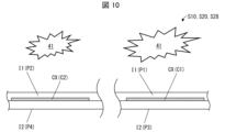
- FIG. 10 is a cross-sectional view showing an example of a method for manufacturing a self-luminous display device according to an embodiment of the present disclosure.
- steps S10 and S20 are performed in order, and then, with the entire upper surface of the first insulating layer I1 exposed, oxygen is introduced into the first insulating layer I1 by the first plasma 41 (step S28).
- This can be achieved by using oxygen in the first plasma 41, and is a so-called "oxygen plasma treatment.”
- the stronger the first plasma 41 is, the greater the amount of oxygen introduced. Specifically, more oxygen is introduced into the first portion P1 located in an area where the strength of the first plasma 41 is strong than into the second portion P2 located in an area where the strength of the first plasma 41 is weak.
- step S30 is performed.
- the annealing process liberates oxygen from the first insulating layer I1, oxidizing the oxide semiconductor contained in the channel layer CX.
- the more oxygen contained in the first insulating layer I1 the more oxygen is liberated, and therefore the more the oxide semiconductor is oxidized.
- the oxide semiconductor contained in the first channel layer C1 is more oxidized than the oxide semiconductor contained in the second channel layer C2. Additionally or alternatively, oxygen reacts with hydrogen, and the more oxygen there is, the less the oxide semiconductor is reduced by hydrogen.
- steps S40, S42, and S44 are performed to remove the template layer 51.
- This manufacturing method also (at least partially) cancels out the effects of the gate length and the degree of reduction of the oxide semiconductor on the transistor threshold, thereby reducing the difference between the design threshold and the actual threshold of the transistor. It also reduces the difference in threshold between the first transistor T1 formed in an area with a strong plasma and the second transistor T2 formed in an area with a weak plasma.
- the self-luminous display device 1 may have the second insulating layer I2 doped with oxygen.
- the self-luminous display device 1 includes the second insulating layer I2 having a third portion P3 in contact with the upper surface of the first channel layer C1 and a fourth portion P4 in contact with the upper surface of the second channel layer C2, and the density of oxygen contained in the fourth portion P4 is smaller than the density of oxygen contained in the third portion P3.
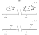
- FIG. 11 is a cross-sectional view showing an example of a method for manufacturing a self-luminous display device according to an embodiment of the present disclosure.
- a second insulating layer I2 is formed on the opposite side of the first insulating layer I1 and in contact with the channel layer CX (step S50).
- the channel layer CX is to be formed on the second insulating layer
- the first insulating layer I1 is to be formed on the channel layer CX.
- oxygen is introduced into the second insulating layer I2 by the third plasma 43 (step S58). This can be achieved by using oxygen for the third plasma 43. More oxygen is introduced into the third portion P3 located in the region where the strength of the third plasma 43 is strong than into the fourth portion P4 located in the region where the strength of the third plasma 43 is weak.
- the channel layer CX and the second insulating layer I2 are annealed (step S60).
- the annealing process liberates oxygen from the second insulating layer I2, oxidizing the oxide semiconductor contained in the channel layer CX. Due to the difference in the amount of oxygen in the third portion P3 and the fourth portion P4, the oxide semiconductor contained in the first channel layer C1 is more oxidized than the oxide semiconductor contained in the second channel layer C2. Additionally or alternatively, oxygen reacts with hydrogen, and the more oxygen there is, the less the oxide semiconductor is reduced by hydrogen. Then, step S10 and the subsequent steps are performed in order. The annealing processes in steps S60 and S30 may be performed in the same process.
- dehydrogenation holes may be formed only in the insulating layer in contact with the lower surface of the channel layer.
- oxygen may be doped only in the insulating layer in contact with the lower surface of the channel layer.
- dehydrogenation holes may be formed in the insulating layer in contact with one surface of the channel layer, and oxygen may be doped in the insulating layer in contact with the other surface.
Landscapes
- Physics & Mathematics (AREA)
- General Physics & Mathematics (AREA)
- Engineering & Computer Science (AREA)
- Theoretical Computer Science (AREA)
- Electroluminescent Light Sources (AREA)
Abstract
本開示に係る自発光型表示装置は、酸化物半導体を含む第1チャネル層(C1)を有する第1トランジスタ(T1)を含む第1画素回路と、第1画素回路と同一回路構成を有し、第1トランジスタ(T1)に対応し、酸化物半導体を含む第2チャネル層(C2)を有する第2トランジスタ(T2)を含む第2画素回路と、を備え、第2トランジスタ(T2)のゲート長(L2)が第1トランジスタ(T1)のゲート長(L1)よりも大きく、第2トランジスタ(T2)が含む酸化物半導体は、第1トランジスタ(T1)が含む酸化物半導体よりも還元されている。
Description
本開示は、自発光型表示装置および自発光型表示装置の製造方法に関する。
特許文献1は、ゲート絶縁膜の膜厚がトランジスタの閾値に影響することを開示している。
トランジスタの閾値は、ゲート長およびチャネル層のキャリア濃度に影響される。このため、トランジスタの実際の閾値がばらつき、表示品位が低下しやすい。
本開示の一態様に係る自発光型表示装置は、酸化物半導体を含む第1チャネル層を有する第1トランジスタを含む第1画素回路と、前記第1画素回路と同一回路構成を有し、前記第1トランジスタに対応し、酸化物半導体を含む第2チャネル層を有する第2トランジスタを含む第2画素回路と、を備え、前記第2トランジスタのゲート長が前記第1トランジスタのゲート長よりも大きく、前記第2チャネル層が含む酸化物半導体は、前記第1チャネル層が含む酸化物半導体よりも還元されている、構成である。
本開示の一態様に係る自発光型表示装置の製造方法は、トランジスタの酸化物半導体を含むチャネル層を形成する工程と、前記チャネル層と接する第1絶縁層を形成する工程と、第1プラズマによって、前記第1絶縁層を貫通する孔を形成するように前記第1絶縁層をエッチングするか、または前記第1絶縁層に酸素を導入する工程と、前記第1プラズマによる工程よりも後に、前記チャネル層および前記第1絶縁層をアニール処理する工程と、前記トランジスタのゲート電極の材料となる導体層を形成する工程と、第2プラズマによって、前記導体層から前記トランジスタのゲート電極を形成するように、前記導体層をエッチングする工程と、を含む方法である。
本開示の一態様によれば、表示装置の表示品位を向上することができる。
〔実施形態1〕
(構成)
図1は、本開示の一実施形態に係る自発光型表示装置の構成例を示す平面図である。図1に示すように、本開示に係る自発光型表示装置1は、複数の画素PXを含む表示部DAと、表示部DAを駆動する駆動回路10と、を備える。複数の画素PXはそれぞれ、発光素子2と、発光素子2に印加する電流または電圧を制御する画素回路3とを有する。画素回路3はそれぞれ、トランジスタTXを含み、トランジスタTXはそれぞれ、酸化物半導体を含むチャネル層を有する。
(構成)
図1は、本開示の一実施形態に係る自発光型表示装置の構成例を示す平面図である。図1に示すように、本開示に係る自発光型表示装置1は、複数の画素PXを含む表示部DAと、表示部DAを駆動する駆動回路10と、を備える。複数の画素PXはそれぞれ、発光素子2と、発光素子2に印加する電流または電圧を制御する画素回路3とを有する。画素回路3はそれぞれ、トランジスタTXを含み、トランジスタTXはそれぞれ、酸化物半導体を含むチャネル層を有する。
自発光型表示装置1は、酸化物半導体を含む第1チャネル層を有する第1トランジスタT1を含む第1画素回路31と、第1画素回路31と同一回路構成を有し、第1トランジスタT1に対応し、酸化物半導体を含む第2チャネル層を有する第2トランジスタT2を含む第2画素回路32と、を備える。第2画素回路32は、より詳細に言えば、設計上、回路素子の配置および接続関係が第1画素回路31と同一であり、対応する回路素子の特性が同一である。回路素子の特性は、例えば、トランジスタの閾値および容量素子の容量値などである。酸化物半導体を用いたトランジスタのゲート電圧の閾値は、周知のように、当該トランジスタのゲート長と、当該トランジスタにおける酸化物半導体の還元の程度と、に依存する。したがって、第1トランジスタT1および第2トランジスタT2は、設計上、閾値が同一であり、ゲート長および還元の程度が同一である。第1トランジスタT1および第2トランジスタT2は、駆動トランジスタであってよい。以降、第1トランジスタT1および第2トランジスタT2に注目する。
図2、図3および図4は、図1に示した、第1トランジスタおよび第2トランジスタの構成例を示す平面透視図、断面図および断面図である。図3は図2のABCD断面を示し、図4は、図2のEFGHIJ断面を示す。図2~図4に示すように、第1トランジスタT1は、ゲート電極G1、ソース電極S1、ドレイン電極D1、および酸化物半導体を含む第1チャネル層C1を有する。第2トランジスタT2は、ゲート電極G2、ソース電極S2、ドレイン電極D2、および酸化物半導体を含む第2チャネル層C2を有する。
第2トランジスタT2の実際のゲート長L2が第1トランジスタT1の実際のゲート長L1よりも大きく、実際の第2チャネル層C2が含む酸化物半導体は、実際の第1チャネル層C1が含む酸化物半導体よりも還元されている。これら実際での差異は、製造プロセスに起因する。以降、「設計上」または「理想的」などと断らない限り、実際の値および差異について述べる。
上記構成によれば、ゲート長L1,L2の差異は、第2トランジスタT2の閾値を第1トランジスタT1の閾値よりも大きくするように作用する。一方、酸化物半導体の還元の程度の差異は、第2トランジスタT2の閾値を第1トランジスタT1の閾値よりも小さくするように作用する。これらの作用が(少なくとも部分的に)打消し合う結果、第1トランジスタT1と第2トランジスタT2との閾値の差異を低減することができる。
比較例として、ゲート長が異なり、酸化物半導体の還元の程度が同一であるトランジスタを考える。この場合、ゲート長の差異が閾値の差異に直結し、閾値の差異が大きい。自発光型表示装置の複数の画素回路において、このように大きな閾値の差異は、輝度ムラを生じさせ、表示品位を悪くする。商業的には通常、出荷前に輝度ムラが視認されなくなる調整(いわゆる「デムラ処理」)を行うが、調整困難な程度の輝度ムラが残ることがある。また、閾値の差異は、経年変化の差異に繋がり、経年変化後に輝度ムラを生じさせ、表示品位を悪くする。
本開示の構成によれば、閾値の差異が小さく、このため、デムラ処理前の素の輝度ムラが小さい。したがって、自発光型表示装置1の表示品位を向上でき、特に経年変化後の表示品位を向上できる。
第1トランジスタT1および第2トランジスタT2はそれぞれ、薄膜トランジスタであってよい。第1チャネル層C1が含む酸化物半導体と、第2チャネル層C2が含む酸化物半導体とは互いに同一材料であってよい。酸化物半導体は、例えば、酸化銅、酸化銀、酸化亜鉛、酸化ガリウム、酸化スズ、酸化インジウム、酸化インジウムガリウム亜鉛、酸化インジウムスズ、酸化インジウム亜鉛、酸化チタン、酸化インジウムチタン、酸化インジウムチタン亜鉛であってよい。ゲート電極G1およびゲート電極G2は、互いと同一層から形成され、第1チャネル層C1および第2チャネル層C2は、互いと同一層から形成される。ソース電極S1,S2およびドレイン電極D1,D2は、互いと同一層から形成されてよい。
自発光型表示装置1は、第1チャネル層C1の上面と接する第1部分P1と、第2チャネル層C2の上面と接する第2部分P2とを有する第1絶縁層I1を備える。第2部分P2が含む水素の密度が、第1部分P1が含む水素に密度よりも大きい。また、第1部分P1の近傍を貫通している第1孔H1の径よりも、第2部分P2の近傍を貫通している第2孔H2の径が小さい。第1孔H1は、第1部分P1から脱水素するための貫通孔であり、第2孔H2は、第2部分P2から脱水素するための貫通孔である。第2孔H2の径が0であってもよく、換言すると、第2部分P2の近傍に脱水素用孔が無くてもよい。第1絶縁層I1は、無機絶縁層であってよく、例えば、窒化シリコン(SiN),酸化シリコン(SiO)、窒酸化シリコン(SiNO)を含んでよい。
(製造方法)
図5は、本開示の一実施形態に係る自発光型表示装置の製造方法の一例を示す断面図である。図5に示すように、まず、トランジスタの酸化物半導体を含む第1チャネル層CXを形成し(ステップS10)、チャネル層CXと接する第1絶縁層I1を形成する(ステップS20)。チャネル層CXは、第1チャネル層C1および第2チャネル層C2を含む。第1絶縁層I1は、チャネル層CXの上に形成される。第1絶縁層I1は、形成された時点で、水素を含有している。
図5は、本開示の一実施形態に係る自発光型表示装置の製造方法の一例を示す断面図である。図5に示すように、まず、トランジスタの酸化物半導体を含む第1チャネル層CXを形成し(ステップS10)、チャネル層CXと接する第1絶縁層I1を形成する(ステップS20)。チャネル層CXは、第1チャネル層C1および第2チャネル層C2を含む。第1絶縁層I1は、チャネル層CXの上に形成される。第1絶縁層I1は、形成された時点で、水素を含有している。
続いて、第1絶縁層I1の上に、開口OXを有するフォトレジスト層21を形成する(ステップS22)。開口OXは、第1孔H1の形成予定位置と重なる第1開口O1と、第2孔H2の形成予定位置と重なる第2開口O2と、を含む。理想的には、第2開口O2の深さおよび径が、第1開口O1の深さおよび径と同一である。開口OXは貫通していないことが有益である。貫通していない開口OXを有するフォトレジスト層21は、ハーフトーンマスクまたはグレートーンマスクを用いて実現できる。
そして、第1プラズマ41によって、第1絶縁層I1を貫通する孔HXを形成するように、フォトレジスト層21および第1絶縁層I1をエッチングし(ステップS24)、フォトレジスト層21を除去する(ステップS26)。開口OXは、平面視で孔HXと重なる。第1絶縁層I1を貫通する孔HXは、第1孔H1および第2孔H2を含む。ステップS24において、第1プラズマ41が強いほど、開口OXおよび孔HXの径が広がる。具体的には、第1プラズマ41の強度が強い領域に形成される第1孔H1の径が、第1プラズマ41が弱い領域に形成される第2孔H2の径よりも大きい。
ステップS22において開口OXが貫通していない場合、ステップS24において、第1プラズマ41によって、開口OXがフォトレジスト層21を貫通するように、フォトレジスト層21をエッチングし、さらに、孔HXを形成するように、第1絶縁層I1をエッチングする。このため、第1孔H1および第2孔H2の径に差異を付けやすい。特に、第2孔H2の径を0にすることができ、換言すると、第1プラズマ41が弱い領域に脱水素用孔を形成しないことができる。
第1プラズマ41による工程よりも後に、チャネル層CXおよび第1絶縁層I1をアニール処理する(ステップS30)。アニール処理によって、水素が第1絶縁層I1から遊離し、遊離した水素の一部はチャネル層CXが含む酸化物半導体を還元し、別の一部は還元せずに逃げる。孔HXの径が大きいほど、水素が孔HXを通って逃げやすく、したがって、孔HXの近傍の酸化物半導体があまり還元されない。具体的には、第1孔H1および第2孔H2の径の差異に起因して、第1部分P1から第1チャネル層C1側へ遊離した水素は、第2部分P2から第2チャネル層C2側へ遊離した水素よりも逃げやすい。したがって、第2チャネル層C2が含む酸化物半導体は、第1チャネル層C1が含む酸化物半導体よりも還元される。
続いて、トランジスタのゲート電極GXの材料となる導体層13を形成し(ステップS40)、導体層13の上にパターニングされたテンプレート層51を形成する(ステップS42)。そして、テンプレート層51に従って、第2プラズマ42によって、導体層13からトランジスタのゲート電極GXを形成するように、導体層13をエッチングし(ステップS44)、テンプレート層51を除去する。ゲート電極GXは、ゲート電極G1およびゲート電極G2を含む。ステップS44において、第2プラズマ42が強いほど、ゲート長が小さい。具体的には、第2プラズマ42が強い領域に形成される第1トランジスタT1のゲート長L1が、第2プラズマ42の強度が弱い領域に形成される第2トランジスタT2のゲート長L2よりも小さい。
この製造方法によれば、トランジスタの閾値に対するゲート長および酸化物半導体の還元の程度の影響が(少なくとも部分的に)打消し合う結果、トランジスタの設計上の閾値と、トランジスタの実際の閾値との差異を低減できる。また、プラズマの強度が強い領域に形成される第1トランジスタT1と、プラズマが弱い領域に形成される第2トランジスタT2との閾値の差異を低減できる。
図6は、図5に示したプラズマの強度分布の一例を示す平面図である。図6に示すように、第1および第2プラズマ41,42はそれぞれ、空間的に不均一な強度分布を有していてよい。典型的には、プラズマ発生するチャンバ40内のうち、中心領域F1および外周領域F2でプラズマが弱く、その間の中間領域F3でプラズマが強い。中間領域F3の形状は、プラズマ発生電極の形状に対応し、通常、円環形状である。第1および第2プラズマ41,42の強度分布は、互いに略同一であることが有益である。具体的には、第1トランジスタT1が形成される領域で、第1および第2プラズマ41,42が強く、第2トランジスタT2が形成される領域で、第1および第2プラズマ41,42が弱いことが有益である。強度分布を測定しても、プラズマ発生装置の構成から強度分布を推定してもよい。プラズマ発生電極の形状および配置が同一である場合、第1および第2プラズマ41,42の強度分布が、同一であると判断できる。また、第1および第2プラズマ41,42を、同一装置によって生成してよい。
〔実施形態2〕
本開示の他の実施形態について、以下に説明する。なお、説明の便宜上、上記実施形態にて説明した部材と同じ機能を有する部材については、同じ符号を付記し、その説明を繰り返さない。
本開示の他の実施形態について、以下に説明する。なお、説明の便宜上、上記実施形態にて説明した部材と同じ機能を有する部材については、同じ符号を付記し、その説明を繰り返さない。
図7は、本開示の一実施形態に係る自発光型表示装置の構成例を示す断面図である。図7に示すように、本開示に係る自発光型表示装置1は、第1チャネル層C1の下面と接する第3部分P3と、第2チャネル層C2の下面と接する第4部分P4とを有する第2絶縁層I2を備える。第4部分P4が含む水素の密度が、第3部分P3が含む水素に密度よりも大きい。また、第3部分P3の近傍を貫通している第3孔H3の径よりも、第4部分P4の近傍を貫通している第4孔H4の径が小さい。第3孔H3は、第3部分P3から脱水素するための貫通孔であり、第4孔H4は、第4部分P4から脱水素するための貫通孔である。第4孔H4の径が0であってもよく、換言すると、第4部分P4の近傍に脱水素用孔が無くてもよい。第2絶縁層I2は、無機絶縁層であってよく、例えば、窒化シリコン(SiN),酸化シリコン(SiO)、窒酸化シリコン(SiNO)を含んでよい。第3孔H3は、平面視で第1孔H1と重なっても、重ならなくてもよい。第4孔H4は、平面視で第2孔H2と重なっても、重ならなくてもよい。
図8は、本開示の一実施形態に係る自発光型表示装置の製造方法の一例を示す断面図である。図8に示すように、第1絶縁層I1と反対側でチャネル層CXと接する第2絶縁層I2を形成する(ステップS50)。図8に示す例において、チャネル層CXは、第2絶縁層の上に形成予定であり、第1絶縁層I1は、チャネル層CXの上に形成予定である。第2絶縁層I2も、形成された時点で、水素を含有している。続いて、第2絶縁層I2の上に、開口OYを有するフォトレジスト層22を形成する(ステップS52)。開口OYは、第3孔H3の形成予定位置と重なる第3開口O3と、第4孔H4の形成予定位置と重なる第4開口O4と、を含む。理想的には、第4開口O4の深さおよび径が、第3開口O3の深さおよび径と同一である。開口OYも貫通していないことが有益である。
そして、第3プラズマ43によって、第2絶縁層I2を貫通する孔HYを形成するように、フォトレジスト層22および第2絶縁層I2をエッチングし(ステップS54)、フォトレジスト層22を除去する(ステップS56)。換言すると、第3プラズマ43によって、開口OYがフォトレジスト層22を貫通するように、フォトレジスト層22をエッチングし、さらに、孔HYを形成するように、第2絶縁層I2をエッチングする。開口OYは、平面視で孔HYと重なる。第2絶縁層I2を貫通する孔HYは、第3孔H3および第4孔H4を含む。第3プラズマ43の強度が強い領域に形成される第3孔H3の径が、第3プラズマ43が弱い領域に形成される第4孔H4の径よりも大きい。第4孔H4の径が0であってもよい。
第3プラズマ43は、空間的に不均一な強度分布を有していてよい。第3プラズマ43の強度分布は、第1および第2プラズマ41,42の強度分布と同一であることが有益である。また、第1~第3プラズマ41~43を、同一装置によって生成してよい。
第3プラズマ43による工程よりも後に、チャネル層CXおよび第2絶縁層I2をアニール処理する(ステップS60)。アニール処理によって、水素が第2絶縁層I2から遊離し、遊離した水素の一部はチャネル層CXが含む酸化物半導体を還元する。そして、ステップS10およびそれ以降のステップを順に行う。ステップS60およびステップS30におけるアニール処理は、同一工程で行われてもよい。換言すると、第1プラズマ41による工程よりも後、かつ、第3プラズマ43により工程よりも後に、チャネル層CX、第1絶縁層I1および第2絶縁層I2をアニール処理してよい。
〔実施形態3〕
図9は、本開示の一実施形態に係る自発光型表示装置の構成例を示す透視平面図である。図9のABCD断面は、図3と同一である。図9に示すように、本開示に係る自発光型表示装置1は、脱水素用孔が、第1チャネル層C1および第2チャネル層C2の近傍に設けられておらず、第1絶縁層I1に酸素をドーピングされている。図3に示すように、自発光型表示装置1は、第1チャネル層C1の上面と接する第1部分P1と、第2チャネル層C2の上面と接する第2部分P2とを有する第1絶縁層I1を備え、第2部分P2が含む酸素の密度が、第1部分P1が含む酸素の密度よりも小さい。
図9は、本開示の一実施形態に係る自発光型表示装置の構成例を示す透視平面図である。図9のABCD断面は、図3と同一である。図9に示すように、本開示に係る自発光型表示装置1は、脱水素用孔が、第1チャネル層C1および第2チャネル層C2の近傍に設けられておらず、第1絶縁層I1に酸素をドーピングされている。図3に示すように、自発光型表示装置1は、第1チャネル層C1の上面と接する第1部分P1と、第2チャネル層C2の上面と接する第2部分P2とを有する第1絶縁層I1を備え、第2部分P2が含む酸素の密度が、第1部分P1が含む酸素の密度よりも小さい。
図10は、本開示の一実施形態に係る自発光型表示装置の製造方法の一例を示す断面図である。図10に示すように、ステップS10,S20を順に行い、続いて、第1絶縁層I1の上面が全て露出した状態で、第1プラズマ41によって、第1絶縁層I1に酸素を導入する(ステップS28)。これは、第1プラズマ41に、酸素を用いることによって、実現でき、いわゆる「酸素プラズマ処理」である。ステップS28において、第1プラズマ41が強いほど、酸素の導入量が多い。具体的には、第1プラズマ41の強度が強い領域に位置する第1部分P1に、第1プラズマ41が弱い領域に位置する第2部分P2によりも、酸素が多く導入される。
そして、ステップS30を行う。アニール処理によって、酸素が第1絶縁層I1から遊離し、チャネル層CXが含む酸化物半導体を酸化する。第1絶縁層I1が含有する酸素が多いほど、遊離する酸素が多く、したがって、酸化物半導体がより酸化される。具体的には、第1部分P1および第2部分P2における酸素量の差異に起因して、第1チャネル層C1が含む酸化物半導体は、第2チャネル層C2が含む酸化物半導体よりも酸化される。加えてまたはあるいは、酸素が水素と反応し、酸素が多いほど、水素による酸化物半導体の還元があまり行われない。
続いて、ステップS40,S42,S44を行い、テンプレート層51を除去する。
この製造方法によっても、トランジスタの閾値に対するゲート長および酸化物半導体の還元の程度の影響が(少なくとも部分的に)打消し合う結果、トランジスタの設計上の閾値と、トランジスタの実際の閾値との差異を低減できる。また、プラズマの強度が強い領域に形成される第1トランジスタT1と、プラズマが弱い領域に形成される第2トランジスタT2との閾値の差異を低減できる。
〔実施形態4〕
図9および図3を再度参照して、本開示に係る自発光型表示装置1は、第2絶縁層I2に酸素をドーピングされていてもよい。自発光型表示装置1は、第1チャネル層C1の上面と接する第3部分P3と、第2チャネル層C2の上面と接する第4部分P4とを有する第2絶縁層I2を備え、第4部分P4が含む酸素の密度が、第3部分P3が含む酸素の密度よりも小さい。
図9および図3を再度参照して、本開示に係る自発光型表示装置1は、第2絶縁層I2に酸素をドーピングされていてもよい。自発光型表示装置1は、第1チャネル層C1の上面と接する第3部分P3と、第2チャネル層C2の上面と接する第4部分P4とを有する第2絶縁層I2を備え、第4部分P4が含む酸素の密度が、第3部分P3が含む酸素の密度よりも小さい。
図11は、本開示の一実施形態に係る自発光型表示装置の製造方法の一例を示す断面図である。図11に示すように、第1絶縁層I1と反対側でチャネル層CXと接する第2絶縁層I2を形成する(ステップS50)。図11に示す例において、チャネル層CXは、第2絶縁層の上に形成予定であり、第1絶縁層I1は、チャネル層CXの上に形成予定である。続いて、第2絶縁層I2の上面が全て露出した状態で、第3プラズマ43によって、第2絶縁層I2に酸素を導入する(ステップS58)。これは、第3プラズマ43に、酸素を用いることによって、実現できる。第3プラズマ43の強度が強い領域に位置する第3部分P3に、第3プラズマ43が弱い領域に位置する第4部分P4によりも、酸素が多く導入される。
第3プラズマ43による工程よりも後に、チャネル層CXおよび第2絶縁層I2をアニール処理する(ステップS60)。アニール処理によって、酸素が第2絶縁層I2から遊離し、チャネル層CXが含む酸化物半導体を酸化する。第3部分P3および第4部分P4における酸素量の差異に起因して、第1チャネル層C1が含む酸化物半導体は、第2チャネル層C2が含む酸化物半導体よりも酸化される。加えてまたはあるいは、酸素が水素と反応し、酸素が多いほど、水素による酸化物半導体の還元があまり行われない。そして、ステップS10およびそれ以降のステップを順に行う。ステップS60およびステップS30におけるアニール処理は、同一工程で行われてもよい。
本開示は上述した各実施形態に限定されるものではなく、請求項に示した範囲で種々の変更が可能であり、異なる実施形態にそれぞれ開示された技術的手段を適宜組み合わせて得られる実施形態についても本開示の技術的範囲に含まれる。さらに、各実施形態にそれぞれ開示された技術的手段を組み合わせることにより、新しい技術的特徴を形成することができる。
例えば、チャネル層の下面と接する絶縁層のみに、脱水素用孔を形成してよい。例えば、チャネル層の下面と接する絶縁層のみに、酸素をドーピングしてよい。例えば、チャネル層の一方面と接する絶縁層に脱水素用孔を形成し、他方面に接する絶縁層に酸素をドーピングしてよい。
1 自発光型表示装置
13 導体層
21、22 フォトレジスト層
31 第1画素回路
32 第2画素回路
41 第1プラズマ
42 第2プラズマ
43 第3プラズマ
C1 第1チャネル層
C2 第2チャネル層
CX チャネル層
G1,G2,GX ゲート電極
H1 第1孔
H2 第2孔
H3 第3孔
H4 第4孔
HX 孔
I1 第1絶縁層
I2 第2絶縁層
L1,L2 ゲート長
OX,OY 開口
T1 第1トランジスタ
T2 第2トランジスタ
P1 第1部分
P2 第2部分
P3 第3部分
P4 第4部分
13 導体層
21、22 フォトレジスト層
31 第1画素回路
32 第2画素回路
41 第1プラズマ
42 第2プラズマ
43 第3プラズマ
C1 第1チャネル層
C2 第2チャネル層
CX チャネル層
G1,G2,GX ゲート電極
H1 第1孔
H2 第2孔
H3 第3孔
H4 第4孔
HX 孔
I1 第1絶縁層
I2 第2絶縁層
L1,L2 ゲート長
OX,OY 開口
T1 第1トランジスタ
T2 第2トランジスタ
P1 第1部分
P2 第2部分
P3 第3部分
P4 第4部分
Claims (20)
- 酸化物半導体を含む第1チャネル層を有する第1トランジスタを含む第1画素回路と、
前記第1画素回路と同一回路構成を有し、前記第1トランジスタに対応し、酸化物半導体を含む第2チャネル層を有する第2トランジスタを含む第2画素回路と、を備え、
前記第2トランジスタのゲート長が前記第1トランジスタのゲート長よりも大きく、前記第2チャネル層が含む酸化物半導体は、前記第1チャネル層が含む酸化物半導体よりも還元されている、自発光型表示装置。 - 前記第1トランジスタおよび前記第2トランジスタはそれぞれ、薄膜トランジスタである、請求項1に記載の自発光型表示装置。
- 前記第1チャネル層が含む酸化物半導体と、前記第2チャネル層が含む酸化物半導体とは互いに同一材料である、請求項1または2に記載の自発光型表示装置。
- 前記第1トランジスタのゲート電極と、前記第2トランジスタのゲート電極とは、互いと同一の層から形成され、
前記第1チャネル層と前記第2チャネル層とは、互いと同一の層から形成されている、請求項1~3の何れか1項に記載の自発光型表示装置。 - 前記第1チャネル層の上面と接する第1部分と、前記第2チャネル層の上面と接する第2部分とを有する第1絶縁層を備え、
前記第2部分が含む水素の密度が、前記第1部分が含む水素の密度よりも大きい、請求項1~4の何れか1項に記載の自発光型表示装置。 - 前記第1チャネル層の上面と接する第1部分と、前記第2チャネル層の上面と接する第2部分とを有する第1絶縁層を備え、
前記第1部分の近傍を貫通している第1孔の径よりも、前記第2部分の近傍を貫通している第2孔の径が小さい、請求項1~5の何れか1項に記載の自発光型表示装置。 - 前記第1チャネル層の上面と接する第1部分と、前記第2チャネル層の上面と接する第2部分とを有する第1絶縁層を備え、
前記第2部分が含む酸素の密度が、前記第1部分が含む酸素の密度よりも小さい、請求項1~4の何れか1項に記載の自発光型表示装置。 - 前記第1チャネル層の下面と接する第3部分と、前記第2チャネル層の下面と接する第4部分とを有する第2絶縁層を備え、
前記第4部分が含む水素の密度が、前記第3部分が含む水素の密度よりも大きい、請求項1~7の何れか1項に記載の自発光型表示装置。 - 前記第1チャネル層の下面と接する第3部分と、前記第2チャネル層の下面と接する第4部分とを有する第2絶縁層を備え、
前記第3部分の近傍を貫通している第3孔の径よりも、前記第4部分の近傍を貫通している第4孔の径が小さい、請求項1~8の何れか1項に記載の自発光型表示装置。 - 前記第1チャネル層の下面と接する第3部分と、前記第2チャネル層の下面と接する第4部分とを有する第2絶縁層を備え、
前記第3部分が含む酸素の密度が、前記第4部分が含む酸素の密度よりも小さい、請求項1~7の何れか1項に記載の自発光型表示装置。 - トランジスタの酸化物半導体を含むチャネル層を形成する工程と、
前記チャネル層と接する第1絶縁層を形成する工程と、
第1プラズマによって、前記第1絶縁層を貫通する孔を形成するように前記第1絶縁層をエッチングするか、または前記第1絶縁層に酸素を導入する工程と、
前記第1プラズマによる工程よりも後に、前記チャネル層および前記第1絶縁層をアニール処理する工程と、
前記トランジスタのゲート電極の材料となる導体層を形成する工程と、
第2プラズマによって、前記導体層から前記トランジスタのゲート電極を形成するように、前記導体層をエッチングする工程と、を含む自発光型表示装置の製造方法。 - 前記第1および第2プラズマはそれぞれ、空間的に不均一な強度分布を有する請求項11に記載の自発光型表示装置の製造方法。
- 前記第1および第2プラズマの強度分布は、互いに同一である、請求項11または12に記載の自発光型表示装置の製造方法。
- 前記第1および第2プラズマを、同一装置によって生成する、請求項11~13の何れか1項に記載の自発光型表示装置の製造方法。
- 前記第1絶縁層の上に、貫通していない開口を有するフォトレジスト層を形成する工程をさらに含み、
前記第1プラズマによって、前記フォトレジスト層および前記第1絶縁層をエッチングする、請求項11~14の何れか1項に記載の自発光型表示装置の製造方法。 - 前記第1プラズマによって、前記開口が前記フォトレジスト層を貫通するように、前記フォトレジスト層をエッチングし、
前記開口は、平面視で前記孔と重なる、請求項15に記載の自発光型表示装置の製造方法。 - 前記第1絶縁層の上面が全て露出した状態で、前記第1プラズマによって前記第1絶縁層に酸素を導入する、請求項11~16の何れか1項に記載の自発光型表示装置の製造方法。
- 前記第1プラズマに酸素を用いる、請求項17の何れか1項に記載の自発光型表示装置の製造方法。
- 前記チャネル層の上に前記第1絶縁層を形成する、請求項11~18の何れか1項に記載の自発光型表示装置の製造方法。
- 前記第1絶縁層と反対側で前記チャネル層と接する第2絶縁層を形成する工程と、
第3プラズマによって、前記第2絶縁層を貫通する孔を形成するように前記第2絶縁層をエッチングするか、または前記第2絶縁層に酸素を導入する工程と、
前記第3プラズマによる工程よりも後に、前記チャネル層および前記第2絶縁層をアニール処理する工程と、をさらに含む請求項11~19の何れか1項に記載の自発光型表示装置の製造方法。
Priority Applications (2)
| Application Number | Priority Date | Filing Date | Title |
|---|---|---|---|
| PCT/JP2023/012359 WO2024201685A1 (ja) | 2023-03-28 | 2023-03-28 | 自発光型表示装置および自発光型表示装置の製造方法 |
| CN202380096426.9A CN120958504A (zh) | 2023-03-28 | 2023-03-28 | 自发光型显示装置和自发光型显示装置的制造方法 |
Applications Claiming Priority (1)
| Application Number | Priority Date | Filing Date | Title |
|---|---|---|---|
| PCT/JP2023/012359 WO2024201685A1 (ja) | 2023-03-28 | 2023-03-28 | 自発光型表示装置および自発光型表示装置の製造方法 |
Publications (1)
| Publication Number | Publication Date |
|---|---|
| WO2024201685A1 true WO2024201685A1 (ja) | 2024-10-03 |
Family
ID=92904256
Family Applications (1)
| Application Number | Title | Priority Date | Filing Date |
|---|---|---|---|
| PCT/JP2023/012359 Ceased WO2024201685A1 (ja) | 2023-03-28 | 2023-03-28 | 自発光型表示装置および自発光型表示装置の製造方法 |
Country Status (2)
| Country | Link |
|---|---|
| CN (1) | CN120958504A (ja) |
| WO (1) | WO2024201685A1 (ja) |
Citations (7)
| Publication number | Priority date | Publication date | Assignee | Title |
|---|---|---|---|---|
| JP2011096958A (ja) * | 2009-11-02 | 2011-05-12 | Seiko Epson Corp | 半導体装置の製造方法 |
| US20120117519A1 (en) * | 2010-11-03 | 2012-05-10 | Texas Instruments Incorporated | Method of transistor matching |
| US20140011329A1 (en) * | 2011-01-18 | 2014-01-09 | Peking University Shenzhen Graduate School | Method for manufacturing self-aligned thin film transistor |
| US20160233253A1 (en) * | 2015-02-09 | 2016-08-11 | Samsung Display Co., Ltd. | Thin film transistor substrate, display apparatus including thin film transistor substrate, method of manufacturing thin film transistor substrate, and method of manufacturing display apparatus |
| JP2020010058A (ja) * | 2009-07-03 | 2020-01-16 | 株式会社半導体エネルギー研究所 | 半導体装置の作製方法 |
| CN111081551A (zh) * | 2019-12-10 | 2020-04-28 | Tcl华星光电技术有限公司 | 阵列基板的制造方法 |
| US20210036126A1 (en) * | 2019-07-31 | 2021-02-04 | Stmicroelectronics (Rousset) Sas | Fabrication process comprising an operation of defining an effective channel length for mosfet transistors |
-
2023
- 2023-03-28 CN CN202380096426.9A patent/CN120958504A/zh active Pending
- 2023-03-28 WO PCT/JP2023/012359 patent/WO2024201685A1/ja not_active Ceased
Patent Citations (7)
| Publication number | Priority date | Publication date | Assignee | Title |
|---|---|---|---|---|
| JP2020010058A (ja) * | 2009-07-03 | 2020-01-16 | 株式会社半導体エネルギー研究所 | 半導体装置の作製方法 |
| JP2011096958A (ja) * | 2009-11-02 | 2011-05-12 | Seiko Epson Corp | 半導体装置の製造方法 |
| US20120117519A1 (en) * | 2010-11-03 | 2012-05-10 | Texas Instruments Incorporated | Method of transistor matching |
| US20140011329A1 (en) * | 2011-01-18 | 2014-01-09 | Peking University Shenzhen Graduate School | Method for manufacturing self-aligned thin film transistor |
| US20160233253A1 (en) * | 2015-02-09 | 2016-08-11 | Samsung Display Co., Ltd. | Thin film transistor substrate, display apparatus including thin film transistor substrate, method of manufacturing thin film transistor substrate, and method of manufacturing display apparatus |
| US20210036126A1 (en) * | 2019-07-31 | 2021-02-04 | Stmicroelectronics (Rousset) Sas | Fabrication process comprising an operation of defining an effective channel length for mosfet transistors |
| CN111081551A (zh) * | 2019-12-10 | 2020-04-28 | Tcl华星光电技术有限公司 | 阵列基板的制造方法 |
Also Published As
| Publication number | Publication date |
|---|---|
| CN120958504A (zh) | 2025-11-14 |
Similar Documents
| Publication | Publication Date | Title |
|---|---|---|
| KR100446272B1 (ko) | 반도체 장치 | |
| CN100510851C (zh) | 制造平板显示器的方法 | |
| US20040016924A1 (en) | Top gate type thin film transistor | |
| KR100731738B1 (ko) | 박막트랜지스터, 평판표시장치 및 그 제조방법 | |
| CN107275340A (zh) | 薄膜晶体管制备方法、阵列基板、其制备方法及显示装置 | |
| US6998640B2 (en) | Thin film transistor structure | |
| JP2020537346A (ja) | Tft基板及びその製造方法 | |
| WO2024201685A1 (ja) | 自発光型表示装置および自発光型表示装置の製造方法 | |
| WO2012005030A1 (ja) | 薄膜トランジスタ、その製造方法、および表示装置 | |
| WO2019104834A1 (zh) | 一种tft阵列基板及其制作方法、显示装置 | |
| TW201351659A (zh) | 薄膜電晶體及其製造方法 | |
| KR100552967B1 (ko) | 이중 버퍼층을 갖는 능동 매트릭스 유기전계발광소자 및그의 제조방법 | |
| KR100507344B1 (ko) | 박막 트랜지스터 및 그의 제조 방법 | |
| KR20090116887A (ko) | 박막트랜지스터 및 그 제조방법 | |
| JP6829775B2 (ja) | 薄膜トランジスタ及びその製造方法、表示パネル | |
| WO2023087373A1 (zh) | 显示面板及其制作方法、移动终端 | |
| CN109638034A (zh) | 显示面板的制造方法 | |
| KR100552936B1 (ko) | 금속 오프셋 영역을 포함하는 결정질 박막트랜지스터의제조 방법 | |
| KR100635580B1 (ko) | 박막트랜지스터, 평판표시장치 및 그 제조방법 | |
| JP2009267296A (ja) | 金属配線の製造方法、tftの製造方法、及びそれを用いて製造されたtft | |
| JPS63289946A (ja) | N↑+非晶質シリコンに対する高歩留りの電気的コンタクトを形成するための方法 | |
| WO2024201684A1 (ja) | 自発光型表示装置および自発光型表示装置の製造方法 | |
| KR100761072B1 (ko) | 평판표시장치와 그 제조방법 | |
| KR100298461B1 (ko) | 반도체 소자 제조방법 | |
| JP2004064056A (ja) | 半導体集積回路の作製方法 |
Legal Events
| Date | Code | Title | Description |
|---|---|---|---|
| 121 | Ep: the epo has been informed by wipo that ep was designated in this application |
Ref document number: 23930325 Country of ref document: EP Kind code of ref document: A1 |
|
| NENP | Non-entry into the national phase |
Ref country code: DE |
|
| 122 | Ep: pct application non-entry in european phase |
Ref document number: 23930325 Country of ref document: EP Kind code of ref document: A1 |