WO2024201638A1 - 制御装置及び制御方法 - Google Patents
制御装置及び制御方法 Download PDFInfo
- Publication number
- WO2024201638A1 WO2024201638A1 PCT/JP2023/012105 JP2023012105W WO2024201638A1 WO 2024201638 A1 WO2024201638 A1 WO 2024201638A1 JP 2023012105 W JP2023012105 W JP 2023012105W WO 2024201638 A1 WO2024201638 A1 WO 2024201638A1
- Authority
- WO
- WIPO (PCT)
- Prior art keywords
- temperature
- semiconductor switching
- switching element
- power conversion
- predetermined
- Prior art date
- Legal status (The legal status is an assumption and is not a legal conclusion. Google has not performed a legal analysis and makes no representation as to the accuracy of the status listed.)
- Ceased
Links
Images



Classifications
-
- H—ELECTRICITY
- H02—GENERATION; CONVERSION OR DISTRIBUTION OF ELECTRIC POWER
- H02M—APPARATUS FOR CONVERSION BETWEEN AC AND AC, BETWEEN AC AND DC, OR BETWEEN DC AND DC, AND FOR USE WITH MAINS OR SIMILAR POWER SUPPLY SYSTEMS; CONVERSION OF DC OR AC INPUT POWER INTO SURGE OUTPUT POWER; CONTROL OR REGULATION THEREOF
- H02M1/00—Details of apparatus for conversion
-
- H—ELECTRICITY
- H02—GENERATION; CONVERSION OR DISTRIBUTION OF ELECTRIC POWER
- H02M—APPARATUS FOR CONVERSION BETWEEN AC AND AC, BETWEEN AC AND DC, OR BETWEEN DC AND DC, AND FOR USE WITH MAINS OR SIMILAR POWER SUPPLY SYSTEMS; CONVERSION OF DC OR AC INPUT POWER INTO SURGE OUTPUT POWER; CONTROL OR REGULATION THEREOF
- H02M7/00—Conversion of AC power input into DC power output; Conversion of DC power input into AC power output
- H02M7/42—Conversion of DC power input into AC power output without possibility of reversal
- H02M7/44—Conversion of DC power input into AC power output without possibility of reversal by static converters
- H02M7/48—Conversion of DC power input into AC power output without possibility of reversal by static converters using discharge tubes with control electrode or semiconductor devices with control electrode
Definitions
- An embodiment of the present invention relates to a control device and a control method.
- a heat sink, cooling device, etc. may be provided to cool the semiconductor switching element, preventing the temperature of the semiconductor switching element from rising excessively.
- the object of the present invention is to provide a control device and control method that can improve the reliability of temperature management of semiconductor switching elements for power conversion.
- the control device of one aspect of the embodiment is a control device for a power conversion device that includes a semiconductor switching element that generates heat due to power conversion, a heat sink for the semiconductor switching element, and a cooling mechanism that cools the heat sink.
- the control device includes an element temperature estimator and a control unit.
- the element temperature estimator derives an estimate of the temperature of the semiconductor switching element using either the drive amount of the semiconductor switching element or the temperature of a predetermined position within a predetermined range from the position of the semiconductor switching element.
- the control unit identifies an abnormal state of the cooling mechanism when the temperature difference between the estimate of the temperature of the semiconductor switching element and the temperature at the predetermined position in the power conversion device exceeds a predetermined threshold temperature.
- the threshold temperature is determined to be lower than the upper limit temperature of the range allowed for the temperature difference and higher than a reference temperature that is predetermined in association with the amount of heat generated by the semiconductor switching element.
- FIG. 1 is a configuration diagram of a power conversion device including a control device according to an embodiment
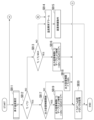
- 4 is a flowchart showing a procedure for identifying a state of a power conversion device according to an embodiment.
- FIG. 4 is a diagram for explaining an arrangement of a temperature sensor according to the embodiment.
- 6 is a diagram for explaining an output capacity limit based on an internal temperature Ta in the embodiment.
- FIG. 5 is a diagram for explaining an output capacitance limit based on an element temperature Tj in the embodiment.
- FIG. 5 is a flowchart of a process for adjusting an output capacity limit value according to the embodiment.
- 5 is a flowchart of a process for adjusting an output capacity limit value according to the embodiment.
- FIG. 2 is an elevational view illustrating a first example of an arrangement of temperature sensors according to the embodiment.
- FIG. 11 is a plan view illustrating a second example of an arrangement of temperature sensors in the embodiment.
- FIG. 11 is an elevational view illustrating a second example of an arrangement of temperature sensors according to the embodiment.
- 5 is a diagram for explaining the relationship between output capacitance and temperature according to the embodiment.
- FIG. FIG. 4 is a diagram for explaining average heat generation according to the embodiment.
- 5A and 5B are diagrams for explaining transient thermal impedance of the heat sink according to the embodiment. 4 is a flowchart of an element temperature estimation process according to the embodiment.
- 5A and 5B are diagrams for explaining diagnosis of the capacity of a cooling device 9 according to the embodiment.
- FIG. 1 is a configuration diagram of a power conversion device 1 including a control device 10 according to an embodiment.
- a power conversion device 1 a three-phase AC power source 2 connected to the power conversion device 1, and an AC motor 3 are shown.
- the three-phase AC power source 2 supplies, for example, three-phase AC power.
- the three-phase AC power source 2 includes a power grid of a power company, a generator, etc.
- the three-phase AC power source 2 supplies the three-phase AC power to the DC conversion unit 4 of the power conversion device 1.
- the AC motor 3 is, for example, a three-phase AC motor. AC power is supplied to the AC motor 3 from the power conversion device 1.
- the power conversion device 1 includes a DC conversion unit 4, a smoothing capacitor 5, an AC conversion unit 6, a current detector 7, temperature sensors 8A and 8B, a cooling device 9, and a control device 10.
- the DC conversion unit 4 is, for example, a rectifier composed of diodes or the like, or a DC conversion circuit including a semiconductor switching element.
- the semiconductor switching element may be an IGBT, a MOSFET, or the like. This semiconductor switching element may be provided with a flywheel diode.
- the DC conversion unit 4 converts AC power input from the three-phase AC power source 2 into DC power and outputs it.
- FIG. 1 shows the DC conversion unit 4 composed of diodes as an example.
- the DC conversion unit 4 may be provided with a heat sink to dissipate heat generated by losses in the diodes, etc.
- the smoothing capacitor 5 stores the power supplied from the DC converter 4 and smoothes the voltage output by the DC converter 4.
- the AC conversion unit 6 is an AC conversion circuit including a semiconductor switching element 6SW.
- An IGBT, a MOSFET, or the like can be used as the semiconductor switching element 6SW.
- a flywheel diode may be provided in this semiconductor switching element 6SW.
- the AC conversion unit 6 converts DC power into three-phase AC power and outputs it.
- FIG. 1 shows an example of a configuration combining an IGBT and a flywheel diode.
- the number of semiconductor switching elements 6SW, etc. in the AC conversion unit 6 is not limited to that shown in the figure, and may be multiple.
- the AC conversion unit 6 is provided with a heat sink 6HS for dissipating heat generated by losses in the semiconductor switching elements 6SW.
- the heat sink 6HS dissipates heat due to losses in the semiconductor switching elements 6SW.
- the current detector 7 is an example of a current transformer including a Hall CT or a shunt resistor.
- the current detector 7 detects the current output to the AC motor 3, and outputs the current value of the detection result to the current detection unit 101.
- the location where the current detector 7 is provided is not limited to the AC bus of two or more of the three phases, and may be a location where the current waveform of the current flowing through the AC conversion unit 6 can be reproduced, for example, inside the AC conversion unit 6, or between the DC conversion unit 4 and the AC conversion unit 6.
- Temperature sensors 8A and 8B include, for example, thermistors, resistance temperature detectors, etc. Temperature sensors 8A and 8B detect the temperature at the locations where they are placed and generate a signal that changes according to the temperature. For example, temperature sensor 8A is placed at a point in power conversion device 1, such as AC conversion unit 6, where the temperature is relatively high. Temperature sensor 8B is placed at a point within the panel of power conversion device 1 that is relatively close to the outside air temperature. Note that the locations of temperature sensors 8A and 8B are not limited to the locations shown in FIG. 1. For example, temperature sensor 8A may be placed anywhere where it is possible to detect a temperature rise due to the output power of power conversion device 1.
- the cooling device 9 cools the heat sink 6HS of the AC conversion unit 6.
- the cooling device 9 includes a fan for air-cooling the heat sink 6HS, a heat exchange system for water-cooling the heat sink 6HS, etc.
- the control device 10 includes an arithmetic unit such as an MCU or FPGA, and its peripheral circuits.
- the arithmetic unit of the control device 10 includes a processor that executes processing by software (programs), or a hardware arithmetic circuit.
- control device 10 includes a current detection unit 101, a current calculation unit 102, a heat sink temperature detection unit 103, a heat sink temperature calculation unit 104, an element temperature estimation unit 105, an internal panel temperature detection unit 106, an internal panel temperature calculation unit 107, an external command receiving unit 108, a memory unit 110, a control unit 120, and a PWM output unit 130.
- the current detection unit 101 includes a conversion unit such as an AD converter, and receives the signal output by the current detector 7, converts the signal into current data for calculation, and outputs it to the current calculation unit 102.
- a conversion unit such as an AD converter
- the current calculation unit 102 receives the current data output by the current detection unit 101, calculates, for example, the effective value of the current based on the current data, and outputs the calculated value to the control unit 120.
- the heat sink temperature detection unit 103 is a conversion unit such as an AD converter, which receives the signal output by the temperature sensor 8, converts it into temperature data for calculation, and outputs it to the heat sink temperature calculation unit 104.
- the heat sink temperature calculation unit 104 receives the temperature data output by the heat sink temperature detection unit 103, calculates, for example, the temperature in degrees Celsius based on the temperature data, and outputs the calculated temperature to the element temperature estimation unit 105.
- the element temperature estimation unit 105 receives the temperature data from the heat sink temperature calculation unit 104 , calculates the junction temperature of the semiconductor switching element 6 SW based on the temperature data, and outputs an estimated value of the junction temperature of the semiconductor switching element 6 SW to the control unit 120 .
- the element temperature estimation unit 105 derives an estimate (first estimate) of the temperature of the semiconductor switching element 6SW using a detected temperature value at a predetermined position within a predetermined range from the position of the semiconductor switching element 6SW.
- the internal temperature detection unit 106 is a conversion unit such as an AD converter that receives the signal output by the temperature sensor 8B, converts it into temperature data for calculation, and outputs it to the internal temperature calculation unit 107.
- the internal panel temperature calculation unit 107 receives the temperature data output by the internal panel temperature detection unit 106, calculates the temperature in degrees Celsius, for example, based on the temperature data, and outputs the detected value of the internal panel temperature (referred to as the internal panel temperature Ta) to the control unit 120.
- the external command receiver 108 receives external command values used to control the AC motor 3, for example, from a higher-level device, and outputs them to the control unit 120.
- the storage unit 110 includes a storage medium such as a semiconductor memory or a magnetic storage device. New data is written to the storage unit 110 by a write process from the control unit 120, and the storage unit 110 retains this data. The storage unit 110 outputs the retained data by a read process from the control unit 120. Each piece of data may be written to the storage unit 110 by a dedicated controller instead of by the control unit 120.
- the control unit 120 performs various processes related to the collection and management of various data, control of the AC conversion unit 6, identification of the state of the power conversion device 1, etc.
- the control unit 120 is involved in controlling the AC conversion unit 6 and performs the following processing. Using various data stored in the memory unit 110 or collected data, the control unit 120 calculates a control amount (e.g., a voltage reference) for PWM control of the AC motor 3 for each control period and outputs the control amount to the PWM output unit 130.
- a control amount e.g., a voltage reference
- the control unit 120 also performs processing related to identifying the state of the power conversion device 1. Details of this will be described later.
- the PWM output unit 130 generates a PWM signal based on the control amount (voltage reference) supplied from the control unit 120 and outputs it to the AC conversion unit 6.
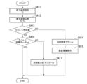
- FIG. 2 is a flowchart showing the procedure for identifying the state of the power conversion device 1 according to the embodiment.
- the control device 10 performs an estimation process (element temperature estimation) of the element temperature Tj using the element temperature estimation unit 105 etc. (SA11).
- the element temperature estimation unit 105 estimates the junction temperature of the semiconductor switching element 6SW based on the temperature data output by the heat sink temperature detection unit 103. The details of this estimation process of the element temperature Tj will be described later.
- the internal panel temperature calculation unit 107 may also perform an estimation process (internal panel temperature estimation) of the internal panel temperature Ta to generate the internal panel temperature (internal panel temperature data) and update the internal panel temperature Ta as the latest estimated value.
- the internal panel temperature Ta may be assumed to be constant. In fact, if an environment is provided in which the internal panel temperature Ta can be assumed to be constant, this estimation process of the internal panel temperature Ta may be omitted.
- the control unit 120 calculates an estimate of the element temperature rise (Tj-Ta) based on the temperature difference between the element temperature Tj and the internal panel temperature Ta (SA12).
- the above element temperature rise (Tj-Ta) is set to, for example, the temperature rise of the element temperature Tj from the reference internal panel temperature Ta.
- the control unit 120 determines whether the element temperature rise (Tj-Ta) is smaller than a predetermined judgment value (SA13).
- the control unit 120 issues a temperature abnormality alarm (temperature abnormality alarm) indicating that the cooling capacity has decreased (SA14), controls the device to a protection operation mode (SA15), and then ends the series of processes.
- a temperature abnormality alarm temperature abnormality alarm
- the control unit 120 identifies whether the element temperature rise (Tj-Ta) is less than a judgment value obtained by adding a predetermined value ⁇ to the value of the initial data (SA16). If the element temperature rise (Tj-Ta) is less than the judgment value obtained by adding a predetermined value ⁇ to the value of the initial data, the control unit 120 ends the series of processes.
- the control unit 120 issues an alarm indicating that the cooling capacity has decreased (a cooling capacity decrease alarm) (SA17), and ends the series of processes.
- the threshold temperature used for the above-mentioned identification may be associated with initial data obtained by operating the semiconductor switching element 6SW in the power conversion device 1.
- the control unit 120 may identify that an abnormality has occurred in the state of the cooling device 9 based on the initial data and an estimated value of the temperature of the semiconductor switching element 6SW.
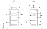
- FIG. 3A is a diagram for explaining the arrangement of the temperature sensor 8A in the embodiment.
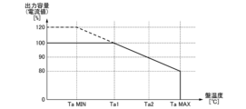
- FIG. 3B is a diagram for explaining the output capacity limit based on the internal panel temperature Ta in the embodiment.
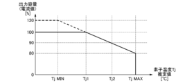
- FIG. 3C is a diagram for explaining the output capacity limit based on the element temperature Tj in the embodiment.
- the panel (housing) of the power conversion device 1 shown in FIG. 3A contains a DC conversion unit 4, a smoothing capacitor 5, an AC conversion unit 6, a cooling device 9, etc. Furthermore, a temperature sensor 8B, etc. are arranged inside the panel (housing) of the power conversion device 1.
- the cooling device 9 in this case may be configured as follows. A case where the cooling device 9 includes an exhaust type fan unit will be described. In this case, the cooling device 9 is arranged to match an opening on the top surface of the board (housing) of the power conversion device 1 (FIG. 3A). An air intake is provided on the door or the like of the board (housing) of the power conversion device 1, and the air intake is provided with a filter for removing dust and preventing insects. The cold air taken in from the air intake absorbs heat while passing through the board (housing), and is exhausted to the outside of the board via the fan unit of the cooling device 9.
- the cooling device 9 may include a blower-type fan unit, in which case the cooling device 9 may be located upstream of the heat sink so as to blow cool air around the heat sink.
- the cooling device 9 may include a water-cooling heat exchanger.
- the cooling device 9 may be arranged such that the heat exchanger is thermally coupled to the heat sink of the heat exchanger 6.
- the cooling device 9 can take a variety of forms. Regardless of the above cases, the temperature sensor 8A may be disposed in the panel (housing) of the power conversion device 1 near the air intake or in a path through which the cool air taken in from the air intake passes.
- the output capacity of the semiconductor switching element 6SW that is permitted within a range below the upper limit (TaMAX) of the internal temperature Ta is specified by a current value.
- the control unit 120 limits the output of the semiconductor switching element 6SW. For example, when the internal temperature Ta is in a range below a first temperature (Ta1), the semiconductor switching element 6SW is permitted to be driven at its rated output capacity (100%).
- the output capacity of the semiconductor switching element 6SW is permitted to be limited below the rated output capacity (100%).
- the control unit 120 derates the output capacity of the semiconductor switching element 6SW to 80%.
- the internal temperature Ta is in the range of not more than the first temperature (Ta1), if certain conditions are satisfied, the semiconductor switching element 6SW is allowed to be driven within the range of exceeding the rated output capacity (100%) up to 120%.
- the limit value of the output capacitance may be derated at a similar reduction rate.
- the predetermined upper limit for limiting the output capacity (drive amount) of the semiconductor switching element 6SW may be determined to be a value exceeding the rated output capacity (100%) of the semiconductor switching element.
- the output capacity of the semiconductor switching element 6SW that is permissible when the junction temperature (referred to as element temperature Tj) of the semiconductor switching element 6SW is within a range below an upper limit value (TjMAX) is specified by a current value.
- the control unit 120 limits the output of the semiconductor switching element 6SW. For example, when the element temperature Tj is in a range not exceeding a first temperature (Tj1), the semiconductor switching element 6SW is permitted to be driven at its rated output capacity (100%).
- the semiconductor switching element 6SW When the element temperature Tj exceeds the first temperature (Tj1) and is in a range not exceeding an upper limit value (TjMAX) of the element temperature Tj, the semiconductor switching element 6SW is permitted to be driven with its output capacity restricted. For example, when the element temperature Tj is the upper limit value (TjMAX) of the element temperature Tj, the output capacity of the semiconductor switching element 6SW is derated (80%). In addition, when the element temperature Tj is in the range below the first temperature (Tj1), if certain conditions are satisfied, the control unit 120 allows the semiconductor switching element 6SW to be driven in the range exceeding the rated output capacity (100%) up to 120%. For example, the control unit 120 may derate the limit value of the output capacitance at a similar reduction rate within the range of the element temperature Tj from the lower limit value (TjMIN) to the upper limit value (TjMAX).
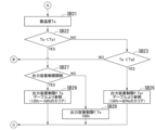
- FIGS. 4A and 4B are flowcharts of a process for adjusting the output capacity limit value according to an embodiment. The processes shown in FIG. 4A and FIG. 4B may be performed independently.
- the control device 10 performs an estimation process (element temperature estimation) of the element temperature Tj by the element temperature estimation unit 105 or the like (SB11).
- This process of SB11 may be the same as the process of SA11 described above, and may be performed as a common process.
- the control unit 120 identifies whether the element temperature Tj is less than the threshold value Tj1 (SB12).
- the control unit 120 identifies whether the element temperature Tj is smaller than the upper limit element temperature TjMAX (SB13).
- the control unit 120 issues a temperature abnormality alarm (SB14), transitions to "device protection operation” to protect the device (SB15), and then ends the series of processes.
- control unit 120 determines the output capacity limit F_Tj to be in the range of 100% to 80% of the rated value (SB16) and proceeds to SB30.
- the control unit 120 determines whether or not to release the output capacity limit (SB17). If the output capacity limit is not released, the control unit 120 sets the output capacity limit F_Tj to rated 100% (SB17) and proceeds to SB30.
- control unit 120 determines the output capacity limit F_Tj to be in the range of the rated value 120 to 100% (SB18) and proceeds to SB30.
- control device 10 can identify the state of the element junction temperature of the power conversion device 1 and adjust the output capacity limit based on the element junction temperature.
- the control device 10 may also perform the process of identifying the "state of temperature inside the panel" shown in FIG. 4B in association with the process of identifying the "state of element junction temperature” shown in FIG. 4A. For example, as shown in FIG. 4B, the control device 10 performs an estimation process of the internal temperature Ta (internal temperature estimation) by using the internal temperature calculation unit 107 etc. (SB21).
- the control unit 120 determines whether the internal panel temperature Ta is lower than the threshold value Ta1 (SB22).
- the control unit 120 identifies whether the internal panel temperature Ta is less than the upper limit internal panel temperature Ta2 (SB23).
- control unit 120 advances the process to SB14 in FIG. 4A described above, issues a temperature abnormality alarm, and moves to "device protection operation" to protect the device, after which the series of processes ends.
- control unit 120 determines the output capacity limit F_Ta to be in the range of 100% to 80% of the rated value (SB26) and proceeds to SB30 in FIG. 4A described above.
- the control unit 120 determines whether or not to release the output capacity limit (SB27). If the output capacity limit is not to be released, the control unit 120 sets the output capacity limit F_Ta to 100% of the rated value (SB27) and proceeds to SB30 in FIG. 4A described above.
- control unit 120 determines the output capacity limit F_Ta to be in the range from 120% to the rated value of 100% (SB28) and proceeds to SB30 in FIG. 4A described above.
- the above process identifies the internal temperature state of the power conversion device 1, making it possible to adjust the output capacity limit based on the internal temperature.
- control unit 120 changes the predetermined upper limit value for limiting the drive amount of the power conversion device 1 depending on whether or not the estimated value of the temperature of the semiconductor switching element 6SW has reached the upper limit temperature of the allowable range. At this time, if the upper limit temperature has been reached, the predetermined upper limit value for limiting the drive amount is maintained, and if the upper limit temperature has not been reached, the restriction imposed by the predetermined upper limit value for limiting the drive amount is relaxed.
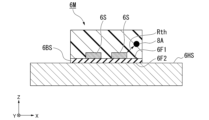
- FIG. 5 is an elevational view for explaining a first example of the arrangement of the temperature sensors according to the embodiment.
- Module 6M is placed on heat sink 6HS.
- This module 6M includes, for example, a substrate 6BS, a semiconductor switching element 6SW, and a temperature sensor 8A.
- the substrate 6BS includes an insulating core material such as ceramic, glass fiber resin, or the like.
- the semiconductor switching element 6SW of the module 6M is disposed on a first surface 6F1 of the substrate 6BS.
- the temperature sensor 8A is disposed in the module 6M.
- the temperature sensor 8A may be disposed within the module 6M.
- the inside of the module 6M is filled with air, resin, or the like.
- the second surface 6F2 of the substrate 6BS of the module 6M is arranged so as to be thermally coupled to the heat sink 6HS.
- a curtain e.g., a curtain made of silicon, mylar, etc.
- Any common method may be selected as the method of thermal coupling.
- a temperature sensor 8A is provided in the module 6M itself.
- a thermal resistance Rth between the installation location of the temperature sensor 8A and a representative position of the semiconductor switching element 6SW is set in advance.
- the control unit 120 uses the thermal resistance Rth to calculate the element temperature Tj of the semiconductor switching element 6SW from the measured temperature of the temperature sensor 8A (referred to as the sensor measured temperature). This calculation may be performed using the following formula (1).
- Element temperature Tj sensor measurement temperature + Rth x average heat generation [W] (1)
- average heat generation [W] in formula (1) may be the average heat generation value of module 6M estimated from the average output current of module 6M.
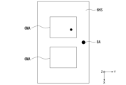
- FIG. 6A is a plan view for explaining a second example of the arrangement of the temperature sensor 8A according to the embodiment.
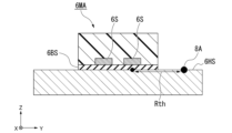
- FIG. 6B is an elevation view for explaining a second example of the arrangement of the temperature sensor 8A according to the embodiment.
- This module 6MA does not include a temperature sensor 8A inside its case. Instead, the temperature sensor 8A is disposed on a heat sink 6HS. Therefore, the thermal conduction characteristics between the installation location of the temperature sensor 8A and the semiconductor switching element 6SW change.
- the thermal resistance for the example shown in Figures 6A and 6B is shown in the following formula (2).
- Rth(h) is the thermal resistance between the installation location of the temperature sensor 8A and the representative position of the module 6M.
- Rth(j-c) is the thermal resistance between the representative position of the module 6M and the representative position of the semiconductor switching element 6SW.
- This representative position of the module 6M may be determined, for example, within the range of an image of the semiconductor switching element 6SW projected onto the surface of the heat sink 6HS. A dot is provided at the representative position of the module 6M. In this way, the definition of the thermal resistance from the heat generating point changes depending on the position of the temperature sensor 8A. Therefore, the above formula (1) is replaced by the following formula (3).
- Element temperature Tj sensor measurement temperature + (Rth(h) + Rth(j-c)) x average heat generation [W] (3)
- the temperature sensor 8A is provided within a predetermined range from the position of the semiconductor switching element 6SW.
- This predetermined range may be within the module 6M including the semiconductor switching element 6SW, or within a range that is determined in advance based on the surface of the heat sink 6HS (on or near the surface).
- the predetermined position is the position (referred to as the first position) of a temperature sensor 8A (first sensor) arranged in a module 6M including a semiconductor switching element 6SW, as shown in FIG.
- the predetermined position is the position (referred to as the second position) of the temperature sensor 8A (second sensor) arranged within a predetermined range (on or near the surface) based on the surface of the heat sink 6HS, as shown in Figures 6A and 6B. In this way, it is advisable to select one of the above depending on the difference between the modules 6M and 6MA to be used.
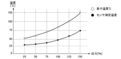
- FIG. 7 is a diagram for explaining the relationship between the output capacitance and temperature in the embodiment.
- the graph shown in Fig. 7 shows the relationship between the output capacitance (horizontal axis) and the temperature measured by the temperature sensor 8A (vertical axis) and the estimated temperature of the semiconductor switching element 6SW (vertical axis).
- the output capacity range shown in this graph is from 0 to 150% when the rated output is 100%.
- the temperature measured by temperature sensor 8A (vertical axis) and the estimated temperature of semiconductor switching element 6SW increase monotonically in an upward sloping manner.
- the estimated temperature of semiconductor switching element 6SW is higher, as shown in the above-mentioned formulas (1) and (3).
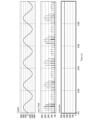
- FIG. 8 is a diagram for explaining average heat generation according to the embodiment.
- the results of simulating heat generation are shown in Fig. 8.
- the upper part of Fig. 8 shows the AC output current (for one phase) of the AC conversion unit 6, the middle part shows the instantaneous heat generation of the semiconductor switching element 6SW, and the lower part shows the average heat generation as a result of taking a moving average of the instantaneous heat generation of the semiconductor switching element 6SW within the range of the AC cycle.
- the instantaneous heat generation of the semiconductor switching element 6SW shown in the middle part was analyzed under the assumption that it occurs based on the sum of the conduction loss and switching loss of the semiconductor switching element 6SW.
- the AC cycle and the magnitude of the output current may be changed continuously. In such applications, it is required to continuously estimate the element temperature Tj more accurately in real time.
- the control signal that characterizes the control of the nearest semiconductor switching element 6SW be handled as a pattern.
- the control signal pattern may specify the operating mode of the AC conversion unit 6.
- the operating modes include a powering mode and a regenerative mode.
- the modulation rate of the PWM control may be used to distinguish between them.
- the average value of the heat generation (average heat generation) is used in the analysis. In order to make this average value of the heat generation more stable, it is advisable to use data for a period of one or more cycles of the AC output frequency and calculate the average of the heat generation data within that period.
- the average heat generation amount is calculated using data for a period shorter than one cycle of the AC output frequency, the total heat generation amount within the period for which the average is calculated will vary depending on whether or not one switching event is included in the period for which the average is calculated, depending on the switching timing of the semiconductor switching element 6SW. Therefore, if a relatively short period is selected, the average heat generation amount obtained will vary depending on whether or not actual switching occurred. In this way, analysis processing that sets a relatively short period is best used when responsiveness is prioritized over estimating an accurate element temperature Tj.
- the "relatively short period” described below is, for example, a period shorter than one second.
- 9 is a diagram for explaining the transient thermal impedance of the heat sink of the embodiment.
- the characteristics of the transient thermal impedance of the heat sink shown in FIG. 9 are modeled for ease of explanation.
- 9 shows an example of the relationship between the average time (LOG scale) and the transient thermal impedance (LOG scale).
- the average time is the width of a time window that defines the target period for which the averaging process is applied. If the averaging time is in the range of 1 second or more, the transient thermal impedance will be a constant value (for example, 1). If the averaging time is shorter than 1 second, the value of the transient thermal impedance will decrease as the averaging time becomes shorter.
- the averaging time may be a fixed value. When changing the averaging time, it is advisable to include the effect of this transient thermal impedance in the calculation conditions. If this effect is not included, the error in the estimated value may become large. Furthermore, since it takes time for the actual device and detection system to completely dissipate the heat it receives, it can be difficult to accurately reproduce a time range of one second or more.
- the average time it is advisable to set the average time to, for example, longer than one second.
- FIG. 10 is a flowchart of the element temperature estimation process according to the embodiment.
- the heat sink temperature detection unit 103 and the heat sink temperature calculation unit 104 detect the temperature of the heat sink 6HS by detecting the temperature using the temperature sensor 8A (SC11).
- the element temperature estimation unit 105 acquires temperature data for the temperature Th corresponding to the measurement result.
- the element temperature estimation unit 105 estimates the output capacitance for the temperature Th and the temperature Tj for that output capacitance using the temperature Th and the information in the table showing the characteristics of the graph shown in FIG. 7 (SC12).
- the control unit 120 also estimates the loss Ploss occurring in the semiconductor switching element 6SW based on the output capacity (current capacity) of the AC supplied to the AC motor 3 and the frequency of the AC (SC13). A general method may be used to estimate the loss Ploss.
- the control unit 120 estimates the temperature Tj using the above-mentioned formula (3) that includes the temperature Th, a predetermined thermal resistance, and the average heat generation of the semiconductor switching element 6SW as variables (SC14). Note that the average heat generation of the semiconductor switching element 6SW changes depending on the magnitude of the loss Ploss in the semiconductor switching element 6SW.
- the control unit 120 acquires the temperature Tj obtained in step SC12 and the temperature Tj obtained in step SC14. The control unit 120 selects the larger value of these two temperatures Tj and determines it as the estimated value of the element temperature Tj. The control unit 120 obtains an estimate of the element temperature Tj through the above processing.
- the element temperature estimation unit 105 derives an estimate (first estimate) of the temperature of the semiconductor switching element 6SW using the detected temperature value at a predetermined position within a predetermined range from the position of the semiconductor switching element 6SW. Furthermore, the control unit 120 derives an element temperature Tj, which is an estimate (second estimate) of the temperature of the semiconductor switching element 6SW, using the drive amount of the semiconductor switching element 6SW. The control unit 120 may use either the first estimated value or the second estimated value to identify an abnormal state of the cooling device 9 (cooling mechanism).
- the capacity of the cooling device 9 may decrease below the capacity in the standard state. In the case of the comparative example, this may lead to an increase in the temperature of the semiconductor switching element 6SW, and as a result, the power conversion device 1 may not be able to continue operating.
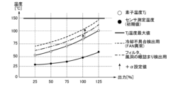
- the estimated result of the element temperature Tj of the semiconductor switching element 6SW is used to diagnose the capacity of the cooling device 9. For example, by detecting that the trend of the temperature rise of the semiconductor switching element 6SW is different from the normal trend, the occurrence of the above-mentioned factors is detected at an early stage. This case will be described with reference to FIG. 3A and FIG. 11.
- FIG. 11 is a diagram for explaining the diagnosis of the capacity of the cooling device 9 of the embodiment.
- the graph shown in FIG. 11 shows the temperature in normal times versus the output (horizontal axis).
- the temperatures shown here show the relationship between the detection result of the temperature sensor 8A, the element temperature Tj of the semiconductor switching element 6SW, and the maximum value of the junction temperature (element temperature Tj).
- the detection result of the temperature sensor 8A and the element temperature Tj of the semiconductor switching element 6SW tend to increase with an increase in output.
- the maximum value of the junction temperature (element temperature Tj) is constant regardless of the output.
- the cooling device 9 includes a cooling fan in its configuration.
- the cooling fan blows cool air around the heat sink 6HS of the semiconductor switching element 6SW. This ventilation improves the heat dissipation efficiency of the heat sink 6HS.
- the temperature sensor 8A and the ventilation direction When the temperature sensor 8A is located upstream of the semiconductor switching element 6SW with respect to the direction of airflow by the cooling fan, the temperature detected by the temperature sensor 8A is lower than the temperature of the semiconductor switching element 6SW. Conversely, when the temperature sensor 8A is located downstream of the semiconductor switching element 6SW, the temperature detected by the temperature sensor 8A will be higher than the temperature when the temperature sensor 8A is located upstream of the semiconductor switching element 6SW. The former is required in order to make the temperature inside the panel Ta equivalent to the air temperature outside the panel.
- initialization data based on the detection results of the temperature sensor 8A can be used. This initialization data is based on test results that also include the conditions of the ventilation direction, and similarly, the thermal resistances in the calculation formulas are also determined with the conditions of the ventilation direction included, so the latter position of the temperature sensor 8A can also be used.
- the ventilation direction and air volume can basically be considered not to change. Even if the internal panel temperature Ta, which is the detection result of the temperature sensor 8A, does not change during operation, the air volume may decrease if the cooling fan fails or the filter becomes clogged. As a result, the heat dissipation efficiency of the heat sink 6HS decreases, and the value of the detection result of the temperature sensor 8B and the estimated value of the element temperature Tj based on this increase.
- the cooling device 9 including such a cooling fan and filter are one example of a cooling mechanism.
- the condition of the cooling device 9 can be diagnosed.
- a threshold for detecting malfunctions in the cooling device 9 can be set at a temperature higher than the line for the estimated value of the element temperature Tj, and a threshold for detecting clogging of the filter and wind tunnel can be set, and these can be used as a reference to detect abnormal temperature increases in the estimated value of the element temperature Tj.
- the control device 10 is a control device for the power conversion device 1.
- the power conversion device 1 includes a semiconductor switching element 6SW that generates heat due to power conversion, a heat sink 6HS for the semiconductor switching element 6SW, and a cooling mechanism for cooling the heat sink 6HS.
- the control device 10 includes an element temperature estimation unit 105 and a control unit 120.
- the element temperature estimation unit 105 derives an estimate of the temperature (element junction temperature) of the semiconductor switching element 6SW using either the drive amount of the semiconductor switching element 6SW or the temperature of a predetermined position within a predetermined range from the position of the semiconductor switching element 6SW.
- the control unit 120 identifies an abnormal state of the cooling device 9 when the temperature difference between the estimated value of the element temperature Tj (element junction temperature) and the temperature (internal temperature Ta) at a predetermined position in the power conversion device 1 exceeds a predetermined threshold temperature, and outputs the identification result.
- the threshold temperature is set to be lower than the upper limit temperature of the range allowed for the temperature difference, and higher than a reference temperature that is predetermined in association with the amount of heat generated by the semiconductor switching element 6SW. This makes it possible to further increase the reliability of temperature management of the semiconductor switching element for power conversion.
- the relationship between the output pattern of the operating power conversion device 1 and the temperature rise of the semiconductor switching element 6SW is stored in the memory unit 110.
- the control unit 120 detects an output pattern that matches or is similar to the output pattern of the power conversion device 1 stored in the memory unit 110. If this occurs as a result of the detection, the control unit 120 compares the temperature rise of the semiconductor switching element 6SW with the temperature rise based on past data, making it easy to determine whether a phenomenon similar to the temperature rise based on past data is occurring.
- the above-mentioned control device 10 includes a temperature sensor 8A (second sensor) arranged within a predetermined range (on the surface or near the surface) based on the surface of the heat sink 6HS, and a temperature sensor 8B (third sensor) arranged at a predetermined position within the panel of the power conversion device 1.
- the element temperature estimation unit 105 derives a first estimate of the temperature of the semiconductor switching element 6SW using the value detected by the temperature sensor 8A.
- the control unit 120 can identify an abnormal state of a cooling mechanism such as the cooling device 9 when the temperature difference between the estimated value of the temperature of the semiconductor switching element 6SW based on the detection value by the temperature sensor 8A and the temperature at a specified position within the panel of the power conversion device 1 based on the detection result by the temperature sensor 8B exceeds a predetermined threshold temperature.
- Second Embodiment A second embodiment will be described.
- a case where one semiconductor switching element 6SW on the heat sink 6HS is operated is described as an example.
- a plurality of semiconductor switching elements 6SW and one temperature sensor 8A may be arranged on the heat sink 6HS.
- the number of semiconductor switching elements 6SW and the number of modules 6MA shown in Figures 6A and 6B are examples.
- an analysis method will be described for a case where a plurality of semiconductor switching elements 6SW are arranged on the heat sink 6HS and each is switched at an appropriate timing.
- Estimation method 1 History data that records the change in temperature when a plurality of semiconductor switching elements 6SW on a heat sink 6HS are operated in a predetermined pattern in advance is used as initial data. For example, one semiconductor switching element 6SW that has the maximum temperature is extracted from the plurality of semiconductor switching elements 6SW based on the initial data. The element temperature Tj of the extracted one semiconductor switching element 6SW is estimated, and the element temperatures of the other semiconductor switching elements 6SW are not estimated. This is sufficient if the element temperature Tj of the semiconductor switching element 6SW with the maximum temperature can be estimated, and the element temperatures of the semiconductor switching elements 6SW other than the semiconductor switching element 6SW with the maximum temperature can be considered to be equal to or lower than the above element temperature Tj.
- Estimation method 2 For example, as shown in the graph of Figure 7 above, if we assume that the temperature outside the panel (housing), i.e., the outside air temperature (Ta0), is 25 degrees, then the temperature inside the panel Ta and the heat sink temperature Th at 0% output will both be 25 degrees.
- the temperature difference ⁇ T between the inside temperature Ta and the heat sink temperature Th and the outside air temperature (Ta0) when each semiconductor switching element 6SW is operated individually is calculated.
- the temperature differences ⁇ T (outside air temperature Ta0-Ta) are added together to obtain ⁇ Ta when the multiple semiconductor switching elements 6SW are operated.
- ⁇ Th when a plurality of semiconductor switching elements 6SW are operated is obtained.
- the temperature difference from the internal panel temperature Ta (Tj-Ta) or the temperature difference from the heat sink temperature Th (Tj-Th) at a certain output is determined in advance.
- the value at the output mentioned above may be used.
- the internal panel temperature Ta may be considered to be 25 degrees.
- Estimation method 3 As with the above-mentioned "Estimation Method 2," it is assumed from the graph in FIG. 7 that "when the outside air temperature (Ta0) of the enclosure is 25 degrees, the internal panel temperature Ta and heat sink temperature Th at 0% output will be 25 degrees.”
- the initial data of the internal temperature Ta when the plurality of semiconductor switching elements 6SW are operated under a predetermined pattern is called ⁇ Ta and ⁇ Th, and the initial data of the heat sink temperature Th is called ⁇ Th.
- the temperature difference (Tj-Ta) from the internal temperature Ta or the temperature difference (Tj-Th) from the heat sink temperature Th when a certain pattern is output is determined in advance. For example, the temperature difference obtained individually by referring to the graph in FIG.
- the control device is a control device for a power conversion device that includes a semiconductor switching element that generates heat due to power conversion, a heat sink for the semiconductor switching element, and a cooling mechanism that cools the heat sink.
- the control device includes an element temperature estimator and a control unit.
- the element temperature estimator derives an estimate of the temperature of the semiconductor switching element using either the drive amount of the semiconductor switching element or the temperature of a predetermined position within a predetermined range from the position of the semiconductor switching element.
- the control unit identifies an abnormal state of the cooling mechanism when the temperature difference between the estimate of the temperature of the semiconductor switching element and the temperature at the predetermined position in the power conversion device exceeds a predetermined threshold temperature.
- the threshold temperature may be determined to be lower than an upper limit temperature of a range allowed for the temperature difference and higher than a reference temperature that is predetermined in association with the amount of heat generated by the semiconductor switching element.
- a part or all of the functional units of the control device 10 in the power conversion device 1 of the embodiment described above may have software functional units that are realized, for example, by a computer processor (hardware processor) executing a program (computer program, software component) stored in a storage unit (memory, etc.) of the computer.
- a part or all of the functional units of the control device 10 may be realized by hardware such as an LSI (Large Scale Integration), an ASIC (Application Specific Integrated Circuit), or an FPGA (Field-Programmable Gate Array), or may be realized by a combination of software functional units and hardware.
Landscapes
- Engineering & Computer Science (AREA)
- Power Engineering (AREA)
- Power Conversion In General (AREA)
- Inverter Devices (AREA)
Priority Applications (3)
| Application Number | Priority Date | Filing Date | Title |
|---|---|---|---|
| JP2025509270A JPWO2024201638A1 (cg-RX-API-DMAC7.html) | 2023-03-27 | 2023-03-27 | |
| CN202380094365.2A CN120752844A (zh) | 2023-03-27 | 2023-03-27 | 控制装置以及控制方法 |
| PCT/JP2023/012105 WO2024201638A1 (ja) | 2023-03-27 | 2023-03-27 | 制御装置及び制御方法 |
Applications Claiming Priority (1)
| Application Number | Priority Date | Filing Date | Title |
|---|---|---|---|
| PCT/JP2023/012105 WO2024201638A1 (ja) | 2023-03-27 | 2023-03-27 | 制御装置及び制御方法 |
Publications (1)
| Publication Number | Publication Date |
|---|---|
| WO2024201638A1 true WO2024201638A1 (ja) | 2024-10-03 |
Family
ID=92904023
Family Applications (1)
| Application Number | Title | Priority Date | Filing Date |
|---|---|---|---|
| PCT/JP2023/012105 Ceased WO2024201638A1 (ja) | 2023-03-27 | 2023-03-27 | 制御装置及び制御方法 |
Country Status (3)
| Country | Link |
|---|---|
| JP (1) | JPWO2024201638A1 (cg-RX-API-DMAC7.html) |
| CN (1) | CN120752844A (cg-RX-API-DMAC7.html) |
| WO (1) | WO2024201638A1 (cg-RX-API-DMAC7.html) |
Cited By (1)
| Publication number | Priority date | Publication date | Assignee | Title |
|---|---|---|---|---|
| WO2026126558A1 (ja) * | 2024-12-09 | 2026-06-18 | 株式会社日立製作所 | 電力変換装置の冷却異常を検知するシステム、検知する演算装置、および検知する方法 |
Citations (4)
| Publication number | Priority date | Publication date | Assignee | Title |
|---|---|---|---|---|
| JP2005124387A (ja) * | 2003-09-26 | 2005-05-12 | Fuji Electric Systems Co Ltd | 同期電動機駆動装置の制御方法 |
| WO2014091852A1 (ja) * | 2012-12-12 | 2014-06-19 | 富士電機株式会社 | 半導体チップ温度推定装置及び過熱保護装置 |
| WO2016035187A1 (ja) * | 2014-09-04 | 2016-03-10 | 三菱電機株式会社 | 異常検出装置及び異常検出方法 |
| WO2019198184A1 (ja) * | 2018-04-11 | 2019-10-17 | 日産自動車株式会社 | 機器保護装置及び機器保護方法 |
Family Cites Families (2)
| Publication number | Priority date | Publication date | Assignee | Title |
|---|---|---|---|---|
| JP2016067164A (ja) * | 2014-09-25 | 2016-04-28 | 株式会社ノーリツ | パワーコンディショナ |
| JP7703837B2 (ja) * | 2020-10-23 | 2025-07-08 | 富士電機株式会社 | 電力変換装置、冷却異常判定装置、冷却異常判定方法 |
-
2023
- 2023-03-27 WO PCT/JP2023/012105 patent/WO2024201638A1/ja not_active Ceased
- 2023-03-27 CN CN202380094365.2A patent/CN120752844A/zh active Pending
- 2023-03-27 JP JP2025509270A patent/JPWO2024201638A1/ja active Pending
Patent Citations (4)
| Publication number | Priority date | Publication date | Assignee | Title |
|---|---|---|---|---|
| JP2005124387A (ja) * | 2003-09-26 | 2005-05-12 | Fuji Electric Systems Co Ltd | 同期電動機駆動装置の制御方法 |
| WO2014091852A1 (ja) * | 2012-12-12 | 2014-06-19 | 富士電機株式会社 | 半導体チップ温度推定装置及び過熱保護装置 |
| WO2016035187A1 (ja) * | 2014-09-04 | 2016-03-10 | 三菱電機株式会社 | 異常検出装置及び異常検出方法 |
| WO2019198184A1 (ja) * | 2018-04-11 | 2019-10-17 | 日産自動車株式会社 | 機器保護装置及び機器保護方法 |
Cited By (1)
| Publication number | Priority date | Publication date | Assignee | Title |
|---|---|---|---|---|
| WO2026126558A1 (ja) * | 2024-12-09 | 2026-06-18 | 株式会社日立製作所 | 電力変換装置の冷却異常を検知するシステム、検知する演算装置、および検知する方法 |
Also Published As
| Publication number | Publication date |
|---|---|
| CN120752844A (zh) | 2025-10-03 |
| JPWO2024201638A1 (cg-RX-API-DMAC7.html) | 2024-10-03 |
Similar Documents
| Publication | Publication Date | Title |
|---|---|---|
| TWI631354B (zh) | 用於功率模組之散熱系統狀況評估之方法及裝置 | |
| US7904254B2 (en) | Power conversion apparatus and method of estimating power cycle life | |
| JP5408136B2 (ja) | インバータ装置、インバータコントロールシステム、モータ制御システム、インバータ装置の制御方法 | |
| KR102963391B1 (ko) | 파워 모듈의 전력 반도체 소자 정션 온도 추정 방법 및 장치 | |
| CN104736981B (zh) | 半导体芯片温度推定装置及过热保护装置 | |
| CN111413604A (zh) | 结温估算方法、装置、电机控制器和车辆 | |
| JP2014187789A (ja) | 異常検出機能を備えたモータ駆動装置 | |
| JP6847158B2 (ja) | 電力変換装置 | |
| BR102014006156A2 (pt) | método para a implementação automática de diagnósticos e prognósticos para acionamentos | |
| JP2016163512A (ja) | インテリジェントパワーモジュールおよびインテリジェントパワーモジュールの評価方法 | |
| CN111466075B (zh) | 电力转换装置 | |
| JP6653122B2 (ja) | 電動圧縮機、制御装置及び監視方法 | |
| CN100570346C (zh) | 检测风冷散热系统散热性能的装置及方法 | |
| CN109830941A (zh) | 新能源汽车igbt模组过温保护策略和装置 | |
| JP5486434B2 (ja) | 電力変換装置 | |
| EP3780375A1 (en) | Diagnostic device and diagnostic system | |
| CN120752844A (zh) | 控制装置以及控制方法 | |
| CN116771507A (zh) | 一种发动机负载的安全供电方法及装置 | |
| JP7259779B2 (ja) | 過電流検出装置 | |
| CN107421762B (zh) | 散热系统诊断方法及装置 | |
| CN102200489A (zh) | 散热系统的诊断方法 | |
| JP2012223062A (ja) | 半導体電力変換装置 | |
| JP7621442B1 (ja) | 電力変換装置及び温度制御方法 | |
| JP2009508461A (ja) | スイッチング電源の動作方法 | |
| JP7743269B2 (ja) | 車両制御装置 |
Legal Events
| Date | Code | Title | Description |
|---|---|---|---|
| 121 | Ep: the epo has been informed by wipo that ep was designated in this application |
Ref document number: 23930278 Country of ref document: EP Kind code of ref document: A1 |
|
| DPE1 | Request for preliminary examination filed after expiration of 19th month from priority date (pct application filed from 20040101) | ||
| WWE | Wipo information: entry into national phase |
Ref document number: 202380094365.2 Country of ref document: CN |
|
| ENP | Entry into the national phase |
Ref document number: 2025509270 Country of ref document: JP Kind code of ref document: A |
|
| WWE | Wipo information: entry into national phase |
Ref document number: 2025509270 Country of ref document: JP |
|
| WWE | Wipo information: entry into national phase |
Ref document number: 202517091103 Country of ref document: IN |
|
| WWP | Wipo information: published in national office |
Ref document number: 202380094365.2 Country of ref document: CN |
|
| WWP | Wipo information: published in national office |
Ref document number: 202517091103 Country of ref document: IN |
|
| NENP | Non-entry into the national phase |
Ref country code: DE |
|
| 122 | Ep: pct application non-entry in european phase |
Ref document number: 23930278 Country of ref document: EP Kind code of ref document: A1 |