WO2024195754A1 - エンコーダ用反射型光学式スケールおよび反射型光学式エンコーダ - Google Patents
エンコーダ用反射型光学式スケールおよび反射型光学式エンコーダ Download PDFInfo
- Publication number
- WO2024195754A1 WO2024195754A1 PCT/JP2024/010429 JP2024010429W WO2024195754A1 WO 2024195754 A1 WO2024195754 A1 WO 2024195754A1 JP 2024010429 W JP2024010429 W JP 2024010429W WO 2024195754 A1 WO2024195754 A1 WO 2024195754A1
- Authority
- WO
- WIPO (PCT)
- Prior art keywords
- encoder
- reflective optical
- optical scale
- metal substrate
- less
- Prior art date
- Legal status (The legal status is an assumption and is not a legal conclusion. Google has not performed a legal analysis and makes no representation as to the accuracy of the status listed.)
- Ceased
Links
Images



Classifications
-
- G—PHYSICS
- G01—MEASURING; TESTING
- G01D—MEASURING NOT SPECIALLY ADAPTED FOR A SPECIFIC VARIABLE; ARRANGEMENTS FOR MEASURING TWO OR MORE VARIABLES NOT COVERED IN A SINGLE OTHER SUBCLASS; TARIFF METERING APPARATUS; MEASURING OR TESTING NOT OTHERWISE PROVIDED FOR
- G01D5/00—Mechanical means for transferring the output of a sensing member; Means for converting the output of a sensing member to another variable where the form or nature of the sensing member does not constrain the means for converting; Transducers not specially adapted for a specific variable
- G01D5/26—Mechanical means for transferring the output of a sensing member; Means for converting the output of a sensing member to another variable where the form or nature of the sensing member does not constrain the means for converting; Transducers not specially adapted for a specific variable characterised by optical transfer means, i.e. using infrared, visible, or ultraviolet light
- G01D5/32—Mechanical means for transferring the output of a sensing member; Means for converting the output of a sensing member to another variable where the form or nature of the sensing member does not constrain the means for converting; Transducers not specially adapted for a specific variable characterised by optical transfer means, i.e. using infrared, visible, or ultraviolet light with attenuation or whole or partial obturation of beams of light
- G01D5/34—Mechanical means for transferring the output of a sensing member; Means for converting the output of a sensing member to another variable where the form or nature of the sensing member does not constrain the means for converting; Transducers not specially adapted for a specific variable characterised by optical transfer means, i.e. using infrared, visible, or ultraviolet light with attenuation or whole or partial obturation of beams of light the beams of light being detected by photocells
- G01D5/347—Mechanical means for transferring the output of a sensing member; Means for converting the output of a sensing member to another variable where the form or nature of the sensing member does not constrain the means for converting; Transducers not specially adapted for a specific variable characterised by optical transfer means, i.e. using infrared, visible, or ultraviolet light with attenuation or whole or partial obturation of beams of light the beams of light being detected by photocells using displacement encoding scales
Definitions
- This disclosure relates to a reflective optical scale for an encoder and a reflective optical encoder.
- Optical encoders have traditionally been used in servo motors and other devices equipped with a control mechanism. There are two types of optical encoders: transmissive and reflective. Reflective encoders have a shorter optical path than transmissive encoders, making them easier to make smaller and thinner. They also have the advantage of being easier to assemble because they do not require positioning of the light-emitting element and light-receiving element.
- a reflective optical encoder comprises a reflective optical scale, a light source such as an LED that irradiates the scale with light, and a photodetector that detects the light reflected from the scale.
- the reflective optical scale has alternating reflective areas (highly reflective areas) and non-reflective areas (lowly reflective areas), and the reflectance of light in the reflective areas is higher than the reflectance of light in the non-reflective areas (see, for example, Patent Document 1).
- the intensity of the light reflected from the scale and incident on the photodetector varies with changes in the position of the scale.
- the photodetector detects the intensity of the light that occurs as the position of the scale moves in the length measurement direction.
- the reflective optical encoder processes displacement information of the position of this scale according to the detected intensity of light, and can obtain position information.
- reflective optical scales are manufactured by singulating a multi-sided mounting body in which multiple reflective optical scales are arranged side by side.
- the base material constituting the multi-sided mounting body is a metal base material
- the metal base material is often singulated by etching in the singulation process, as this has good processing accuracy.
- singulation by etching a metal base material is disadvantageous in terms of cost.
- a bridge is usually provided on the outer periphery of the reflective optical scale to connect the reflective optical scale to the frame. After etching, the bridge is cut to separate the scale into individual reflective optical scales. In this case, bridge marks are left on the reflective optical scale. The bridge marks become burrs and protrusions, causing partial distortion in the reflective optical scale.
- the present invention was made in consideration of the above circumstances, and its main objective is to provide a reflective optical scale for an encoder that can suppress waviness.
- One embodiment of the present disclosure provides a reflective optical scale for an encoder having a disk-shaped metal substrate having a first surface and a second surface opposing the first surface, and a low-reflection layer arranged in a pattern along the circumferential direction of the metal substrate on the first surface side of the metal substrate, wherein the thickness of the metal substrate is 0.3 mm or more and 1.1 mm or less, and the waviness of the reflective optical scale for an encoder is 30 ⁇ m or less.
- Another embodiment of the present disclosure provides a reflective optical encoder comprising the above-mentioned reflective optical scale for an encoder, a light source that irradiates measurement light onto the surface of the reflective optical scale for an encoder on which the low-reflection layer is disposed, and a photodetector that detects reflected light from the reflective optical scale for an encoder.
- the reflective optical scale for encoders disclosed herein has the advantage of being able to suppress waviness.
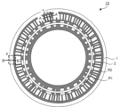
- FIG. 1 is a schematic top view illustrating a reflective optical scale for an encoder in the present disclosure.
- FIG. 2 is a partially enlarged cross-sectional view illustrating a reflective optical scale for an encoder in the present disclosure.
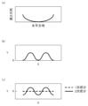
- 1A and 1B are schematic diagrams illustrating undulations of a reflective optical scale for an encoder.
- 1A and 1B are schematic diagrams illustrating undulations of a reflective optical scale for an encoder.
- 1 is a schematic cross-sectional view illustrating a reflective optical scale for an encoder according to the present disclosure.
- 1 is a schematic perspective view illustrating a reflective optical encoder according to the present disclosure.
- FIG. 2 is a schematic top view illustrating a reflective optical scale polygonal body for an encoder according to the present disclosure.
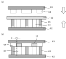
- 1 is a schematic cross-sectional view illustrating a punching device used in a singulation process in a manufacturing method for a reflective optical scale for an encoder in the present disclosure.
- the present disclosure includes embodiments of a reflective optical scale for an encoder and a reflective optical encoder.
- embodiments of the present disclosure will be described with reference to the drawings.
- the present disclosure can be implemented in many different forms, and should not be interpreted as being limited to the description of the embodiments exemplified below.
- the drawings may show the width, thickness, shape, etc. of each part in a schematic manner compared to the actual form, but these are merely examples and do not limit the interpretation of the present disclosure.
- elements similar to those described above with respect to the previous figures may be given the same reference numerals, and detailed explanations may be omitted as appropriate.
- the term “above” or “below” includes both cases in which another component is placed directly above or below a certain component so as to be in contact with the component, and cases in which another component is placed above or below a certain component with another component in between, unless otherwise specified.
- the term “on the surface side” or “on the surface” includes both cases in which another component is placed directly above or below a certain component so as to be in contact with the component, and cases in which another component is placed above or below a certain component with another component in between, unless otherwise specified.
- the "reflective optical scale for encoder” may be simply referred to as the "optical scale.”
- a reflective optical scale for an encoder in the present disclosure is a reflective optical scale for an encoder having a disk-shaped metal substrate having a first surface and a second surface opposing the first surface, and a low-reflection layer arranged in a pattern along the circumferential direction of the metal substrate on the first surface side of the metal substrate, wherein the thickness of the metal substrate is 0.3 mm or more and 1.1 mm or less, and the waviness of the reflective optical scale for an encoder is 30 ⁇ m or less.
- FIG. 1 is a schematic top view showing an example of a reflective optical scale for an encoder in the present disclosure.
- FIG. 2(a) is an enlarged cross-sectional view of the A-A line of the dotted frame a portion of FIG. 1.
- the reflective optical scale for an encoder 10 has a disk-shaped metal substrate 1 having a first surface 1a and a second surface 1b facing the first surface 1a, and a low-reflection layer 2 arranged in a pattern along the circumferential direction of the metal substrate 1 on the first surface 1a side of the metal substrate 1.
- the thickness T1 of the metal substrate 1 is within a predetermined range.
- the reflective optical scale for an encoder 10 has a holed disk shape, and low-reflection regions R2, which are regions where the low-reflection layer 2 is provided, and high-reflection regions R1, which are regions where the low-reflection layer 2 is not provided, are arranged alternately in the circumferential direction.
- the low-reflection regions R2 have the metal substrate 1 and the low-reflection layer 2 in the thickness direction of the reflective optical scale for an encoder 10.
- the high-reflection regions R1 have the metal substrate 1.
- the reflectance of light in the high-reflection region R1 is higher than the reflectance of light in the low-reflection region R2. Note that the reflectance of light in the high-reflection region R1 and the reflectance of light in the low-reflection region R2 indicate the reflectance at the same wavelength and the same angle of incidence.
- the thickness of the metal substrate is within a predetermined range, and is relatively thick, thereby suppressing waviness and warping. Furthermore, since the waviness of the reflective optical scale for an encoder is equal to or less than a predetermined value, the accuracy of the reflective optical scale for an encoder can be improved, and the accuracy of a reflective optical encoder equipped with the reflective optical scale for an encoder can be improved.
- the reflective optical scale for encoders in the present disclosure is preferably manufactured by punching a polygonal body, as described below.
- punching a polygonal body unlike etching a polygonal body, there is no need to provide a bridge connecting the reflective optical scale for encoders and the frame, so no bridge marks are left. This makes it possible to suppress the occurrence of partial distortion.
- Waviness of the reflective optical scale for an encoder is 30 ⁇ m or less, preferably 20 ⁇ m or less, and more preferably 15 ⁇ m or less.
- the accuracy of a reflective optical encoder equipped with the reflective optical scale for an encoder can be improved.
- the smaller the waviness the better, and there is no particular lower limit.
- the "waviness" of the reflective optical scale for encoders is defined as follows. First, a circle of a given radius R is drawn with the center of the reflective optical scale for encoders as its center, and a three-dimensional measuring machine is used to acquire data on the locus of the circle, with the circumferential component being X and the height component being Y. Next, a Fourier transform is performed, and the difference between the maximum and minimum values of the Y component for the second-order component is defined as the waviness.
- the coordinate measuring machine acquires data as shown in FIG. 3(b).
- the first and second order components are obtained as shown in FIG. 3(c).
- the coordinate measuring machine acquires data as shown in FIG. 4(b).
- the first and second order components are obtained as shown in FIG. 4(c).
- the difference between the maximum and minimum values of the Y component for the first order component in FIG. 4(c) may be larger.
- the difference between the maximum and minimum values of the Y component for the second-order component is approximately the same. Therefore, by using the second-order component, the waviness can be appropriately evaluated regardless of the state in which the reflective optical scale for an encoder is placed when measuring the waviness.
- the primary component has a period of one rotation, even if the difference between the maximum and minimum values of the Y component for the primary component is relatively large, it may be possible to correct it in a reflective optical encoder equipped with a reflective optical scale for an encoder.
- the secondary component has a period of 1/2 rotation, it is difficult to correct it in a reflective optical encoder equipped with a reflective optical scale for an encoder. Therefore, it can be said that waviness can be appropriately evaluated by using the secondary component.
- distaltion of the reflective optical scale for an encoder refers to a state in which the surface of the reflective optical scale for an encoder is significantly rough in a partial area of the surface of the reflective optical scale for an encoder. Distortion also refers to a spacing that is smaller than that of waviness. Specifically, distortion is defined as a spacing that is 1/10 or less (mm) of the outer diameter of the reflective optical scale for an encoder, or 2.5 mm, whichever is larger.
- the waviness is determined by the following method. First, a circle with a radius of 10.5 mm is drawn with the center of the reflective optical scale for the encoder as the center, and data is acquired on the locus of the circle with the circumferential component as X and the height component as Y using a three-dimensional measuring machine. Next, a Fourier transform is performed, and the difference between the maximum and minimum values of the Y component for the secondary component is taken as the waviness. Note that if the outer diameter of the reflective optical scale for the encoder is small, it may not be possible to draw the circle with a radius of 10.5 mm.
- the radius of the reflective optical scale for the encoder is 10.5 mm or less, the radius of the circle is determined as the radius of the reflective optical scale for the encoder multiplied by 0.875.
- the reflective optical scale for the encoder is a perforated disk and the inner diameter of the reflective optical scale for the encoder is large, it may not be possible to draw the circle with a radius of 10.5 mm. Therefore, if the inner radius of the reflective optical scale for encoders is 10.5 mm or more, a circle is drawn 5 mm inward from the outer circumference of the reflective optical scale for encoders, centered on the center of the reflective optical scale for encoders.
- a one-shot 3D shape measuring machine VR-6000 series manufactured by Keyence Corporation is used as the three-dimensional measuring machine.
- the measurement surface is the surface on the low-reflection layer side of the reflective optical scale for encoders.
- waviness and “distortion” are distinguished from the surface property parameters defined in JIS B0601:2013.
- the following surface property parameters are defined: profile curve parameters (Pa, Pz, etc.) obtained from a profile curve, roughness parameters (Ra, Rz, etc.) obtained from a roughness curve, and waviness parameters (Wa, Wz, etc.) obtained from a waviness curve.
- the profile curve, roughness curve, and waviness curve are curves obtained by applying a profile curve filter to a measured profile curve.
- the profile curve parameters, roughness parameters, and waviness parameters are obtained from the reference length portion of the profile curve.
- the profile curve parameters, roughness parameters, and waviness parameters can be said to represent the surface property in the microscopic region.
- “waviness” is obtained by applying a Fourier transform as described above.
- “waviness” is determined by the above method, and can be said to represent the height difference in the macroscopic area of the reflective optical scale for encoders. Therefore, "waviness” is different from the surface quality parameters defined in JIS B0601:2013.
- Methods for adjusting the waviness of a reflective optical scale for an encoder include, for example, when punching a multi-sided body as described below, adjusting the waviness of the metal substrate that constitutes the multi-sided body, and adjusting the hardness of the punching blade.
- the waviness of the metal substrate to be processed is small, the waviness of the reflective optical scale for the encoder will also be small. Specifically, the waviness of the metal substrate to be processed is 30 ⁇ m or less, may be 20 ⁇ m or less, or may be 10 ⁇ m or less.
- the method for determining the waviness of the metal substrate to be processed is the same as the method for determining the waviness of the reflective optical scale for the encoder described above.
- the reflective optical scale for an encoder in the present disclosure is usually used as an optical scale for a rotary encoder.
- the reflective optical scale for an encoder is disk-shaped.
- the reflective optical scale for an encoder may be, for example, a perforated disk-shaped scale having a central hole, or may not have a central hole.
- the outer diameter of the reflective optical scale for an encoder in a planar view is, for example, 15 mm or more, and may be 20 mm or more.
- the outer diameter of the reflective optical scale for an encoder is, for example, 70 mm or less, and may be 60 mm or less.
- the outer diameter of the reflective optical scale for an encoder is, for example, 15 mm or more and 70 mm or less, and may be 20 mm or more and 60 mm or less.
- the inner diameter of the reflective optical scale for the encoder is, for example, 5 mm or more and 20 mm or less in plan view.
- the outer diameter of the reflective optical scale for the encoder is calculated from the coordinates of three points. Specifically, three points are selected on the outer circumference of the reflective optical scale for the encoder, an approximation circle is calculated from the coordinates of the three points, and the diameter of the approximation circle is taken as the outer diameter.
- the inner diameter of the reflective optical scale for the encoder is calculated from three-point coordinates. Specifically, three points are selected on the inner circumference of the reflective optical scale for the encoder, an approximation circle is calculated from the three-point coordinates, and the diameter of the approximation circle is taken as the inner diameter.
- the process capability index Cp which indicates the inner diameter dimensional accuracy of the reflective optical scale for an encoder, is preferably 1.33 or more, and more preferably 1.6 or more. If the process capability index Cp is within the above range, the inner diameter dimensional accuracy is excellent. Therefore, when attaching the reflective optical scale for an encoder to a rotating shaft, it is possible to suppress misalignment between the center of the rotating shaft and the center of the reflective optical scale for an encoder, i.e., eccentricity. This reduces eccentricity errors and improves the accuracy of the reflective optical encoder.
- the process capability index Cp which indicates the inner diameter dimensional accuracy of the reflective optical scale for encoder, is calculated from the standard deviation by the following formula.
- ⁇ is the standard deviation
- U is the upper limit specification value
- L is the lower limit specification value
- A is the reference value
- ⁇ is the difference between the upper limit specification value or the lower limit specification value and the reference value, i.e., the tolerance.
- the standard deviation ⁇ is found from the measured values of the inner diameters of five samples.
- the tolerance ⁇ is set to 0.015. This is because if the tolerance ⁇ is greater than 0.015 mm, the eccentricity error increases and the accuracy of the reflective optical encoder deteriorates.
- the inner diameter dimensional tolerance of the reflective optical scale for an encoder is preferably, for example, 0.007 mm or less.
- the inner diameter dimensional tolerance refers to the difference between the maximum and minimum values of the inner diameter measurements of the five samples.
- the method for determining the inner diameter measurements of the five samples is as described above.
- the accuracy of the punching die can be adjusted.
- the process capability index Cp which indicates the outer diameter dimensional accuracy of the reflective optical scale for the encoder, is preferably 1.33 or more.
- the process capability index Cp is in the above range, the following advantages are obtained.
- the reflective optical scale for the encoder is fixed using an adhesive.
- the adhesive often overflows. Therefore, the overflowing adhesive may creep up and contaminate the surface of the reflective optical scale for the encoder, which may result in a decrease in the encoder accuracy, i.e., the reading accuracy.
- the outermost peripheral edge of the low reflection layer may be disposed inward in the reflective optical scale for the encoder.
- the process capability index Cp which indicates the outer diameter dimensional accuracy of the reflective optical scale for the encoder, is 1.33 or more so that there is a certain space between the outermost peripheral edge of the low reflection layer and the outer diameter of the reflective optical scale for the encoder.
- the method for calculating the process capability index Cp which indicates the outer diameter dimensional accuracy of the reflective optical scale for an encoder, is the same as the method for calculating the process capability index Cp, which indicates the inner diameter dimensional accuracy of the reflective optical scale for an encoder described above.
- the difference between the outer diameter and the inner diameter i.e., the outer/inner diameter difference
- the outer/inner diameter difference is, for example, 8 mm or more and 13 mm or less. If the outer/inner diameter difference is within the above range, undulation and warping of the optical scale that occurs during punching can be suppressed.
- the thickness of the metal substrate is 0.3 mm or more, preferably 0.32 mm or more, and more preferably 0.35 mm or more. By setting the thickness of the metal substrate within the above range, undulation and warping can be suppressed. In addition, if the thickness of the metal substrate is within the above range, the strength as a reflective optical scale for an encoder is sufficient. On the other hand, the thickness of the metal substrate is 1.1 mm or less, preferably 0.50 mm or less, more preferably 0.47 mm or less, and even more preferably 0.45 mm or less. If the thickness of the metal substrate is within the above range, the reflective optical scale for an encoder can be manufactured by punching the polygonal body.
- the thickness of the metal substrate is 0.3 mm or more and 1.1 mm or less, preferably 0.32 mm or more and 0.50 mm or less, more preferably 0.32 mm or more and 0.47 mm or less, and even more preferably 0.35 mm or more and 0.45 mm or less.
- the thickness of the metal substrate refers to the average thickness of the metal substrate.
- the "thickness" of each component refers to the thickness obtained by a general measurement method.
- Examples of thickness measurement methods include a stylus method in which the thickness is calculated by tracing the surface with a stylus to detect unevenness, and an optical method in which the thickness is calculated based on a spectral reflectance spectrum.
- the thickness can be measured using a stylus film thickness meter "P-15" manufactured by KLA Tencor.
- the thickness is calculated by averaging the thickness measurements at multiple points on the component in question. For example, in the case of a metal substrate, the average thickness measurement at two points symmetrical about the center of a disk-shaped metal substrate can be used.
- the metal substrate in the present disclosure is disk-shaped.
- the metal substrate may be, for example, a perforated disk-shaped substrate having a central hole, or may not have a central hole.
- the outer diameter of the metal substrate in plan view is, for example, 15 mm or more, and may be 20 mm or more.
- the outer diameter of the metal substrate is, for example, 70 mm or less, and may be 60 mm or less.
- the outer diameter of the metal substrate may be, for example, 15 mm or more, 70 mm or less, and 20 mm or more, and 60 mm or less.
- the inner diameter of the metal substrate in plan view is, for example, 5 mm or more and 20 mm or less.
- the difference between the outer diameter and the inner diameter i.e., the outer/inner diameter difference
- the outer/inner diameter difference is, for example, 8 mm or more and 13 mm or less. If the outer/inner diameter difference is within the above range, undulation and warping of the optical scale that occurs during punching can be suppressed.
- the reflectance of the first surface of the metal substrate is, for example, 50% or more, may be 55% or more, or may be 60% or more.
- the reflectance of the first surface of the metal substrate is, for example, 100% or less.
- the reflectance of the first surface of the metal substrate is, for example, 50% or more and 100% or less, may be 55% or more and 100% or less, or may be 60% or more and 100% or less. If the reflectance is within the above range, the difference between the reflectance in the high reflection region and the reflectance in the low reflection region becomes large, thereby preventing erroneous detection by the photodetector and improving the detection accuracy of the signal.
- reflectance refers to the reflectance for the detection light used in the optical encoder.
- the wavelength of the light incident on the first surface of the metal layer is anywhere in the range of 500 nm or more and 1000 nm or less, it is more preferable that the reflectance at an incident angle in the range of 5° or more and 70° or less is within the above range.
- a Shimadzu SolidSpec 3700DUV ultraviolet-visible-near infrared spectrophotometer is used.
- the irradiation beam size is approximately 6mm x 15mm. Both P-polarized and S-polarized light are measured, and the sum is averaged to calculate the 45° linear polarization and the reflectance.
- the metal substrate may have a sagging on the outer peripheral edge on the first surface side.
- FIG. 2(b) is an enlarged cross-sectional view of the B-B line of the dotted frame b in FIG. 1.
- the metal substrate 1 has a sagging P on the outer peripheral edge on the first surface 1a side.
- a reflective optical scale for an encoder having a sagging on the outer peripheral edge on the first surface side of the metal substrate is usually manufactured by punching a polygonal body. Therefore, as described above, no bridge marks are generated, and partial distortion can be suppressed.
- the metal substrate can be made thick, and waviness and warping can be suppressed. In addition, it is advantageous in terms of cost.
- the metal substrate is a perforated disk, it may have a sagging on the inner peripheral edge on the first surface side.
- the material of the metal substrate is preferably one that satisfies the above-mentioned reflectance, and examples thereof include stainless steel (SUS), copper, and aluminum.
- the low reflection layer in the present disclosure is disposed on the first surface side of the metal base in a pattern along the circumferential direction of the metal base.
- the reflectance of light incident on the low reflection region which is a region where a low reflection layer is provided, may be lower than the reflectance of light incident on the high reflection region where no low reflection layer is provided.
- the reflectance of the low reflection region may be lower than the reflectance of the first surface of the metal base material.
- the reflectance at any wavelength in the range of 500 nm to 1000 nm is, for example, 10% or less, may be 5% or less, or may be 1% or less.
- the reflectance of the low reflection region is, for example, 0% or more.
- the reflectance of the low reflection region is, for example, 0% or more and 10% or less, may be 0% or more and 5% or less, or may be 0% or more and 1% or less. If the reflectance is within the above range, the difference between the reflectance in the high reflection region and the reflectance in the low reflection region can be increased.
- the wavelength of the incident light is anywhere in the range of 500 nm or more and 1000 nm or less, it is more preferable that the reflectance at an incident angle anywhere in the range of 5° or more and 70° or less is within the above range.
- the low reflection layer is not particularly limited in structure as long as it satisfies the above reflectance.
- the low reflection layer preferably has a metal chromium film, and a chromium oxide film and a chromium nitride film arranged in random order on the side of the metal chromium film opposite to the metal substrate from the metal substrate side.
- Such a three-layered low reflection layer can reduce the reflectance of the low reflection region to the above range.
- a chromium oxide film and a chromium nitride film can be easily formed by using reactive sputtering or the like.
- the above-mentioned low reflection layer can easily perform high-definition patterning compared to a silicon oxide film.
- a chromium oxide film and a chromium nitride film arranged in any order on the surface of the metal chromium film opposite the metal substrate means that they may be arranged in the order of a metal chromium film, a chromium oxide film, and a chromium nitride film, or in the order of a metal chromium film, a chromium nitride film, and a chromium oxide film.
- the low-reflection layer 2 has, from the metal substrate 1 side, a metal chromium film 2c, a chromium nitride film 2b, and a chromium oxide film 2a.
- the low-reflection layer 2 has, from the metal substrate 1 side, a metal chromium film 2c, a chromium oxide film 2a, and a chromium nitride film 2b.
- the film located on the outermost surface opposite the metal substrate is preferably a chromium oxide film or a chromium nitride film, and more preferably a chromium oxide film. This is because it can more effectively reduce the reflectance of the low-reflection region.
- the "low-reflection layer in which a metal chromium film, a chromium nitride film, and a chromium oxide film are arranged in this order" will be referred to as the first specification low-reflection layer
- the "low-reflection layer in which a metal chromium film, a chromium oxide film, and a chromium nitride film are arranged in this order” will be referred to as the second specification low-reflection layer.
- a metal chromium film, a chromium nitride film, and a chromium oxide film are arranged in this order from the metal substrate side.
- the reflectance at any wavelength in the range of 500 nm to 1000 nm can be reduced to 5% or less, particularly 0.5% or less.
- the change in reflectance with respect to the change in wavelength is gradual, making it easy to control the reflectance.
- the metal chromium film is disposed on the first surface of the metal substrate.
- the metal chromium film is a layer made of metal chromium.
- the metal chromium film is a layer that does not substantially transmit light irradiated from a light source, and preferably has a transmittance of 0.0% or more and 1.0% or less. The transmittance is measured using a spectrophotometer "MPC-3100" manufactured by Shimadzu Corporation.
- the thickness of the metal chromium film is, for example, preferably 40 nm or more, more preferably 70 nm or more.
- Methods for forming metal chromium films include physical vapor deposition (PVD) methods such as sputtering, ion plating, and vacuum deposition.
- PVD physical vapor deposition
- Chromium nitride film The chromium nitride film in this specification is disposed between the metallic chromium film and the chromium oxide film. Unlike chromium oxide nitride and chromium oxide nitride carbide, the chromium nitride film is mainly composed of chromium and nitrogen and does not substantially contain impurities other than chromium and nitrogen.
- x which represents the atomic ratio of Cr to N, is preferably 0.4 or more and 1.1 or less.
- the percentage of chromium and nitrogen is preferably 80 atomic % or more and 100 atomic % or less, and more preferably 90 atomic % or more and 100 atomic % or less.
- the chromium nitride film may contain impurities such as hydrogen, oxygen, and carbon.
- the thickness (T N ) of the chromium nitride film is preferably, for example, 5 nm or more and 100 nm or less, more preferably 10 nm or more and 80 nm or less.
- the sum of T N and T O is preferably 40 nm or more.
- the sum of T N and T O is preferably 20 nm or more.
- the thickness of the chromium nitride film is preferably 10 nm or more and 80 nm or less. It becomes easy to reduce the reflectance in the entire range from green to infrared, that is, the reflectance in the range of about 500 nm to 1000 nm.
- Chromium nitride can be formed by physical vapor deposition (PVD) methods such as reactive sputtering, ion plating, and vacuum deposition.
- PVD physical vapor deposition
- nitrogen is introduced into argon (Ar) gas, and a chromium nitride film can be formed by reactive sputtering using a Cr target.
- Ar argon
- the composition of the chromium nitride film can be controlled by controlling the ratio of Ar gas and nitrogen gas.
- Chromium oxide film The chromium oxide film in this specification is disposed on the opposite side of the chromium nitride film to the metallic chromium film.
- the chromium oxide film is mainly composed of chromium and oxygen, and unlike chromium oxide nitride and chromium oxide nitride carbide, it does not substantially contain impurities other than chromium and oxygen.
- y which represents the atomic ratio of Cr to O, is preferably 1.4 or more and 2.1 or less.
- the ratio of chromium and oxygen is preferably 80 atomic % or more and 100 atomic % or less, and more preferably 90 atomic % or more and 100 atomic % or less.
- the chromium oxide film may contain impurities such as hydrogen, nitrogen, and carbon.
- the thickness of the chromium oxide film is not particularly limited, and is preferably, for example, 5 nm to 100 nm, and more preferably 10 nm to 80 nm.
- the sum of the thickness of the chromium oxide film and the thickness of the chromium nitride film is as described above.
- the thickness of the chromium oxide film is preferably 10 nm to 65 nm. This makes it easier to reduce the reflectance over the entire range from green to infrared, that is, the reflectance over the range of about 500 nm to 1000 nm.
- Chromium oxide can be formed by physical vapor deposition (PVD) methods such as reactive sputtering, ion plating, and vacuum deposition.
- PVD physical vapor deposition
- oxygen is introduced into argon (Ar) gas, and a chromium oxide film can be formed by reactive sputtering using a Cr target.
- the composition of the chromium oxide film can be controlled by controlling the ratio of Ar gas and oxygen gas.
- a metal chromium film, a chromium oxide film, and a chromium nitride film are arranged in this order from the metal substrate side.
- the reflectance at any wavelength in the range of 500 nm to 1000 nm can be reduced to 5% or less, particularly 1% or less.
- metal chromium film in this specification is similar to the metal chromium film in the low reflection layer in the first specification described above, and therefore a description thereof will be omitted here.
- Chromium Oxide Film The chromium oxide film in this specification is disposed between the metallic chromium film and the chromium nitride film.
- the thickness of the chromium oxide film is not particularly limited, and is preferably, for example, 5 nm to 60 nm, and more preferably 10 nm to 50 nm. As described below, it is also preferable that the sum of the thickness of the chromium oxide film and the thickness of the chromium nitride film is within a specified range. Furthermore, the thickness of the chromium oxide film is preferably 5 nm to 35 nm, since this makes it easier to reduce the reflectance over the entire range from green to infrared, that is, the reflectance over the range of approximately 500 nm to 1000 nm.
- the physical properties, composition and formation method of the chromium oxide film are the same as those of the chromium oxide film in the low-reflection layer of the first specification above, so a detailed explanation is omitted here.
- Chromium Nitride Film The chromium nitride film in this specification is disposed on the opposite side of the chromium oxide film to the metallic chromium film.
- the thickness of the chromium nitride film (T N ) is not particularly limited, and is preferably, for example, 5 nm or more and 100 nm or less, and more preferably 10 nm or more and 80 nm or less. Furthermore, in relation to the thickness of the chromium oxide film (T O ), when the wavelength is 850 nm, the sum of T N and T O is preferably 30 nm or more, and when the wavelength is 550 nm, the sum of T N and T O is preferably 15 nm or more. Furthermore, the thickness of the chromium nitride film is preferably 10 nm or more and 60 nm or less. It becomes easy to reduce the reflectance in the entire range from green to infrared, that is, the reflectance in the range of about 500 nm to 1000 nm.
- the method for forming the chromium nitride film is the same as that for the chromium nitride film in the low-reflection layer of the first specification above, so a detailed explanation is omitted here.
- the method for forming the low reflective layer is not particularly limited, but the low reflective layer can be formed by selective etching or lift-off.
- a metal chromium film is first formed on the first surface of the metal substrate by a method such as sputtering, and then a chromium nitride film and a chromium oxide film are formed.
- the metal chromium film, the chromium nitride film, and the chromium oxide film are patterned by photolithography and etching.
- a resist pattern is first formed on the first surface of the metal substrate, and a known vacuum film-forming method such as sputtering is used to form a metal chromium film, a chromium nitride film, and a chromium oxide film.
- the resist pattern is then removed to lift off the metal chromium film, chromium nitride film, and chromium oxide film formed directly on the resist pattern, thereby obtaining patterns of the metal chromium film, chromium nitride film, and chromium oxide film.
- the reflective optical scale for an encoder according to the present disclosure preferably does not have a low-reflection layer in a region extending from the outer circumferential surface of the metal substrate to a depth of 500 ⁇ m inward. This makes it possible to suppress peeling or cracking of the low-reflection layer.
- the distance between the outer peripheral surface of the metal substrate and the outer peripheral surface of the low-reflection layer is preferably 500 ⁇ m or more, more preferably 550 ⁇ m or more, and even more preferably 600 ⁇ m or more. If the distance is within the above range, peeling and cracking of the low-reflection layer can be easily suppressed.
- the distance is preferably, for example, 1500 ⁇ m or less, more preferably 1000 ⁇ m or less, and even more preferably 900 ⁇ m or less. If the distance is within the above range, the increase in size of the reflective optical scale for encoders can be suppressed.
- the distance is, for example, preferably 500 ⁇ m or more and 1500 ⁇ m or less, more preferably 550 ⁇ m or more and 1000 ⁇ m or less, and even more preferably 600 ⁇ m or more and 900 ⁇ m or less.
- the reflective optical scale for an encoder according to the present disclosure may have other layers in addition to the above-mentioned metal substrate and low-reflection layer.
- the reflective optical scale for an encoder according to the present disclosure may have a protective layer between the metal substrate and the low-reflection layer.
- the protective layer is preferably transparent and has a function of protecting the metal substrate.
- the protective layer may be provided over the entire area of the metal substrate in a plan view, or may be provided over a partial area.
- the material for the protective layer is not particularly limited as long as it is transparent and can protect the metal substrate, and can be either an organic material or an inorganic material.
- the organic material preferably contains a resin.
- the resin used in the protective layer is not particularly limited as long as it is a resin that can provide a transparent protective layer.
- ionizing radiation curable resins that are cured by exposure to ionizing radiation such as ultraviolet rays or electron beams, and thermosetting resins that are cured by heating are included.
- novolac resins, polyolefin resins, polyester resins, urethane resins, polyimide resins, acrylic resins, and epoxy resins are preferred.
- phenol novolac resins are preferred. This is because they have excellent electrical properties and can suppress defects caused by charging.
- the acrylic resins trifunctional or higher acrylates such as pentaerythritol tetraacrylate and dipentaerythritol tetraacrylate are preferred. This is because they can enhance photocuring properties.
- epoxy resins epoxy acrylate resins having a fluorene structure are preferred. This is because they improve heat resistance, adhesion, and chemical resistance.
- cardo epoxy resins are also preferred. This is because they can provide excellent transparency, heat resistance, surface hardness, and flatness.
- the organic material may contain a polymerization initiator and various additives.
- inorganic materials include inorganic compounds.
- inorganic compounds include oxides, oxynitrides, nitrides, oxycarbides, and oxycarbonitrides of metal elements or nonmetal elements such as silicon, aluminum, magnesium, calcium, potassium, tin, sodium, titanium, boron, yttrium, zirconium, cerium, and zinc. Silicon dioxide (SiO 2 ) is particularly preferred.
- the inorganic compounds may be used alone or in any combination of the above materials.
- the manufacturing method of a reflective optical scale for an encoder in the present disclosure preferably includes a multi-sided body manufacturing step of manufacturing a multi-sided body having a first surface and a second surface opposing the first surface, the multi-sided body having a thickness of 0.3 mm or more and 1.1 mm or less, a patterned low-reflection layer that is multi-sidedly attached to the first surface side of the metal substrate to be processed and arranged in a circumferential shape, the multi-sided body having a planned outer circumferential punching line for the reflective optical scale for an encoder outside the outer circumferential surface of each of the low-reflection layers, and a waviness of 30 ⁇ m or less, and a singulation step of punching out the multi-sided body along the planned outer circumferential punching line to singulate the multi-sided body, thereby obtaining the reflective optical scale for an encoder.
- FIG. 7 is a schematic top view showing an example of a multi-faceted body according to the present disclosure.
- the multi-faceted body 50 has a metal substrate 51 to be processed having a thickness within a predetermined range, and a patterned low-reflection layer 2 arranged in a circular shape and multi-faceted on the first surface side of the metal substrate 51 to be processed.
- the multi-faceted body 50 has a planned outer periphery punching line L for the reflective optical scale for an encoder arranged outside the outer periphery of each low-reflection layer 2. In the singulation process, the reflective optical scale for an encoder is obtained by punching along the planned outer periphery punching line L to singulate the body.
- a multi-sided body which has a metal substrate to be processed, which has a first surface and a second surface opposite the first surface, and a thickness of 0.3 mm or more and 1.1 mm or less, and patterned low-reflection layers which are multi-sidedly attached to the first surface side of the metal substrate to be processed and are arranged in a circular pattern, with a planned peripheral punching line for a reflective optical scale for an encoder outside the outer circumferential surface of each of the low-reflection layers, and with a waviness of 30 ⁇ m or less.
- the waviness of the polygonal body is similar to that of the reflective optical scale for the encoder described above.
- the thickness of the metal substrate to be processed is the same as the thickness of the metal substrate described above.
- the reflectance of the first surface of the metal substrate to be processed is the same as the reflectance of the first surface of the metal substrate described above.
- the size of the metal substrate to be processed in a plan view is not particularly limited as long as it is large enough to allow the patterned low-reflection layer to be applied to multiple surfaces.
- the method for attaching the patterned low-reflection layer to the first surface of the metal substrate to be processed is the same as the method for forming the low-reflection layer described above.
- the planned outer periphery punching line L of the reflective optical scale for the encoder is arranged outside the outer periphery of each low-reflection layer 2.
- the distance D1 between the planned outer periphery punching line L of the reflective optical scale for the encoder and the outer periphery of the low-reflection layer 2 is preferably, for example, 500 ⁇ m or more, more preferably 550 ⁇ m or more, and particularly preferably 600 ⁇ m or more. If the distance D1 is within the above range, peeling and cracking of the low-reflection layer during punching can be suppressed.
- the distance D1 is preferably, for example, 1500 ⁇ m or less, more preferably 1000 ⁇ m or less, and even more preferably 900 ⁇ m or less. If the distance D1 is within the above range, the increase in size of the reflective optical scale for the encoder can be suppressed. Specifically, the distance D1 is preferably, for example, 500 ⁇ m or more and 1500 ⁇ m or less, more preferably 550 ⁇ m or more and 1000 ⁇ m or less, and even more preferably 600 ⁇ m or more and 900 ⁇ m or less.
- the polygonal mounting body for manufacturing the perforated disc-shaped reflective optical scale for the encoder may have an inner peripheral punching line for punching out the center hole of the reflective optical scale for the encoder.
- FIG. 8(a) and 8(b) are schematic diagrams showing an example of a punching device used in the singulation process.
- the multi-faceted body 50 is placed on the lower stage 62 having the lower blade 61.
- the lower stage 62 is moved upward and the upper stage 63 having the upper blade 64 is moved downward and pressed in, punching out the multi-faceted body 50.
- the position of the upper blade 64 is aligned with the planned outer peripheral punching line and the planned inner peripheral punching line of the multi-faceted body 50.
- a pressing member 65 is disposed in a position opposite the upper blade 64. During punching, the metal substrate to be processed is sandwiched between the upper blade 64 and the pressing member 65, and punching can be performed with less burrs and sagging. In this way, individual reflective optical scales for encoders 10 are obtained.
- the clearance width is preferably, for example, 0.020 mm or less, more preferably 0.017 mm or less, and even more preferably 0.015 mm or less. If the clearance width is within the above range, peeling and cracking of the low-reflection layer during punching can be suppressed. On the other hand, the clearance width is preferably, for example, 0.003 mm or more, more preferably 0.004 mm or more, and even more preferably 0.006 mm or more. By having the clearance width within the above range, the load on the blade of the punching device can be reduced.
- the clearance width is, for example, preferably 0.003 mm or more and 0.020 mm or less, more preferably 0.004 mm or more and 0.017 mm or less, and even more preferably 0.006 mm or more and 0.015 mm or less.
- the clearance width refers to the widthwise distance C between the end face of the upper blade 64 and the end face of the lower blade 61 as shown in FIG. 8(b).
- a reflective optical encoder includes the above-described reflective optical scale for an encoder, a light source that irradiates measurement light onto a surface of the reflective optical scale for an encoder on which the low-reflection layer is disposed, and a photodetector that detects reflected light from the reflective optical scale for an encoder.
- FIG. 6 is a schematic perspective view showing an example of a reflective optical encoder according to the present disclosure.
- the reflective optical encoder 100 includes a reflective optical scale 10 for an encoder, a light source 21, and a photodetector 22.
- a fixed slit 23 is disposed between the photodetector 22 and the reflective optical scale 10 for an encoder.
- the accuracy of the reflective optical encoder can be improved by providing the above-mentioned reflective optical scale for the encoder.
- Reflective optical scale for encoder The reflective optical scale for encoder is similar to that described in "A. Reflective optical scale for encoder" above, and therefore description thereof will be omitted here.
- Light Source examples include LEDs (light emitting diodes) and lasers.
- the wavelength ⁇ of light emitted from the light source is, for example, in the green to infrared region, that is, about 500 nm or more and 1000 nm or less.
- the angle of incidence of the light with respect to the optical scale is, for example, 5° or more and 70° or less.
- the photodetector detects light reflected by the optical scale.
- the photodetector includes a light receiving element such as a photodiode or an image sensor.
- An example of the light receiving element is a photoelectric conversion element.
- the reflective optical encoder according to the present disclosure may include a fixed slit between the photodetector and the reflective optical scale for the encoder. By providing a fixed slit, the change in the amount of light received by the photodetector increases, and the detection sensitivity can be improved.
- the fixed slit may be provided between the light source and the reflective optical scale for the encoder.
- the multi-faceted reflective optical scale body for encoder in the present disclosure has a first surface and a second surface opposing the first surface, and includes a metal substrate to be processed having a thickness of 0.3 mm or more and 1.1 mm or less, and a patterned low-reflection layer that is circumferentially arranged and multi-faceted on the first surface side of the metal substrate to be processed, and has a planned peripheral punching line for the reflective optical scale for encoder outside the outer circumferential surface of each of the low-reflection layers, and has a waviness of 30 ⁇ m or less.
- the polygonal reflective optical scale for encoders in this disclosure is similar to the content described above in "A. Reflective optical scale for encoders 6. Manufacturing method of reflective optical scale for encoders," so a description of it will be omitted here.
- Example 1 First, a 0.37 mm thick SUS substrate was prepared and mirror-finished. A protective layer was formed by applying a protective layer resin composition containing a cardo epoxy resin to the mirror-finished surface of the SUS substrate and curing the composition. Next, a low-reflection layer having a metal chromium layer, a chromium nitride layer, and a chromium oxide layer in this order from the protective layer side was formed in a pattern. This resulted in a multi-faceted body.
- the multi-faceted body was roughly cut so that the outer diameter was about 100 mm to 250 mm.
- the optical alignment marks were used for alignment, and the roughly cut work was punched along the planned outer peripheral punching lines and the planned inner peripheral punching lines. In this way, a reflective optical scale for an encoder was obtained.
- the design value of the outer diameter was 24 mm, and the design value of the inner diameter was 15 mm.
- Example 2 A reflective optical scale for an encoder was produced in the same manner as in Example 1, except that the design value of the inner diameter was set to 6 mm.
- Example 3 A reflective optical scale for an encoder was produced in the same manner as in Example 1, except that the thickness of the SUS substrate was 0.30 mm.
- Example 4 A reflective optical scale for an encoder was produced in the same manner as in Example 1, except that the thickness of the SUS substrate was 1.10 mm.
- Example 1 A reflective optical scale for an encoder was produced in the same manner as in Example 1, except that the polygonal body was subjected to etching instead of punching.
- Example 2 A reflective optical scale for an encoder was produced in the same manner as in Example 1, except that the thickness of the SUS substrate was 0.20 mm and that the polygonal body was etched instead of punched.
- Example 3 A reflective optical scale for an encoder was produced in the same manner as in Example 1, except that the thickness of the SUS substrate was 1.20 mm and that the polygonal body was etched instead of punched.
- Process capability index Cp indicating the inner diameter dimensional accuracy of the reflective optical scale for encoders
- the process capability index Cp which indicates the inner diameter dimensional accuracy of the reflective optical scale for an encoder, was determined by the method described above in "A. Reflective optical scale for encoder, 2. Shape of reflective optical scale for encoder”.
- a reflective optical encoder was manufactured using a reflective optical scale for an encoder. The period, pulse width, and inter-pulse phase difference of the encoder output waveform were measured for the reflective optical encoder, and the degree of error and variation was confirmed by comparing with the design values. The evaluation criteria are shown below. A: The accuracy was sufficient. B: The accuracy was slightly lacking. C: The precision was insufficient.
- a disk-shaped metal substrate having a first surface and a second surface opposite to the first surface; a low-reflection layer disposed in a pattern along a circumferential direction of the metal base on the first surface side of the metal base;
- a reflective optical scale for an encoder comprising: The thickness of the metal substrate is 0.3 mm or more and 1.1 mm or less, The reflective optical scale for an encoder has a waviness of 30 ⁇ m or less.
- the reflective optical scale for an encoder according to [1] which is a perforated disk having a central hole.
- Reference Signs List 1 Metal substrate 2: Low reflection layer 10: Reflective optical scale for encoder 50: Polyhedral reflective optical scale body for encoder 100: Reflective optical encoder
Landscapes
- Physics & Mathematics (AREA)
- General Physics & Mathematics (AREA)
- Optical Transform (AREA)
Abstract
本開示は、第1面、および上記第1面に対向する第2面を有する、円盤状の金属基材と、上記金属基材の上記第1面側に、上記金属基材の円周方向に沿ってパターン状に配置された低反射層と、を有する、エンコーダ用反射型光学式スケールであって、上記金属基材の厚さが、0.3mm以上、1.1mm以下であり、上記エンコーダ用反射型光学式スケールのうねりが、30μm以下である、エンコーダ用反射型光学式スケールを提供する。
Description
本開示は、エンコーダ用反射型光学式スケールおよび反射型光学式エンコーダに関する。
従来、制御機構を備えるサーボモータ等に光学式エンコーダが使用されている。光学式エンコーダには、透過型エンコーダと反射型エンコーダがあるが、反射型エンコーダは透過型エンコーダに比べて光路が短く、小型化、薄型化が容易であり、また、発光素子や受光素子の位置決めが不要であり組み立てが容易であるという利点を有する。
反射型光学式エンコーダは、反射型光学式スケール、スケールに光を照射するLED等の光源、およびスケールからの反射光を検出する光検出器を備える。反射型光学式スケールは、反射領域(高反射領域)と非反射領域(低反射領域)が交互に配置され、反射領域における光の反射率は、非反射領域における光の反射率よりも高い(例えば、特許文献1)。これにより、スケールから反射し光検出器に入射する光の強さは、スケールの位置の変化により強弱を生じる。光検出器は、スケールの位置が測長方向に移動することによって生じる光の強弱を検出する。反射型光学式エンコーダは、検出された光の強弱にしたがって、このスケールの位置の変位情報を処理し、位置情報を取得しうる。
従来、反射型光学式スケールは、複数の反射型光学式スケールが並んで配置されている多面付け体を個片化することによって製造される。多面付け体を構成する基材が金属基材である場合、個片化工程においては、加工精度が良好であることから、金属基材のエッチング加工によって個片化する場合が多い。しかし、金属基材のエッチング加工による個片化は、コスト面で不利である。
そこで、金属基材の厚さを薄くすることで、エッチングコストを削減することが検討されている。また、金属基材の厚さが薄いほうが、精度良くエッチング加工できる。しかし、金属基材が薄いと、反射型光学式スケールの取り扱いが困難になる。また、金属基材が薄いと、金属基材自体にうねりや反りが生じやすいため、反射型光学式スケールにうねりや反りが生じる場合がある。また、金属基材のエッチング加工の場合、通常、反射型光学式スケールの外周には、反射型光学式スケールとフレームとを繋ぐブリッジが設けられる。エッチング加工後にブリッジを切断することで、個々の反射型光学式スケールに分離する。この場合、反射型光学式スケールにブリッジ痕が生じる。ブリッジ痕はバリや突起となり、反射型光学式スケールに部分的に歪みが発生する。
本発明は、上記事情に鑑みてなされたものであり、うねりを抑制することが可能なエンコーダ用反射型光学式スケールを提供することを主目的とする。
本開示の一実施形態は、第1面、および上記第1面に対向する第2面を有する、円盤状の金属基材と、上記金属基材の上記第1面側に、上記金属基材の円周方向に沿ってパターン状に配置された低反射層と、を有する、エンコーダ用反射型光学式スケールであって、上記金属基材の厚さが、0.3mm以上、1.1mm以下であり、上記エンコーダ用反射型光学式スケールのうねりが、30μm以下である、エンコーダ用反射型光学式スケールを提供する。
本開示の他の実施形態は、上述のエンコーダ用反射型光学式スケールと、上記エンコーダ用反射型光学式スケールの上記低反射層が配置された側の表面に、測定光を照射する光源と、上記エンコーダ用反射型光学式スケールからの反射光を検出する光検出器と、を備える、反射型光学式エンコーダを提供する。
本開示におけるエンコーダ用反射型光学式スケールにおいては、うねりを抑制することが可能であるという効果を奏する。
本開示は、エンコーダ用反射型光学式スケールおよび反射型光学式エンコーダを実施態様に含む。以下、本開示の実施態様を、図面等を参照しながら説明する。ただし、本開示は多くの異なる態様で実施することが可能であり、下記に例示する実施の形態の記載内容に限定して解釈されるものではない。また、図面は説明をより明確にするため、実際の形態に比べ、各部の幅、厚さ、形状等について模式的に表わされる場合があるが、あくまで一例であって、本開示の解釈を限定するものではない。また、本明細書と各図において、既出の図に関して前述したものと同様の要素には、同一の符号を付して、詳細な説明を適宜省略することがある。
本明細書において、ある部材の上に他の部材を配置する態様を表現するにあたり、単に「上に」、あるいは「下に」と表記する場合、特に断りの無い限りは、ある部材に接するように、直上、あるいは直下に他の部材を配置する場合と、ある部材の上方、あるいは下方に、さらに別の部材を介して他の部材を配置する場合との両方を含む。また、本明細書において、ある部材の面に他の部材を配置する態様を表現するにあたり、単に「面側に」または「面に」と表記する場合、特に断りの無い限りは、ある部材に接するように、直上、あるいは直下に他の部材を配置する場合と、ある部材の上方、あるいは下方に、さらに別の部材を介して他の部材を配置する場合との両方を含む。
また、本明細書において、「エンコーダ用反射型光学式スケール」を単に「光学式スケール」と称する場合がある。
以下、本開示におけるエンコーダ用反射型光学式スケール、反射型光学式エンコーダ、およびエンコーダ用反射型光学式スケール多面付け体について詳細に説明する。
A.エンコーダ用反射型光学式スケール
本開示におけるエンコーダ用反射型光学式スケールは、第1面、および上記第1面に対向する第2面を有する、円盤状の金属基材と、上記金属基材の上記第1面側に、上記金属基材の円周方向に沿ってパターン状に配置された低反射層と、を有する、エンコーダ用反射型光学式スケールであって、上記金属基材の厚さが、0.3mm以上、1.1mm以下であり、上記エンコーダ用反射型光学式スケールのうねりが、30μm以下である。
本開示におけるエンコーダ用反射型光学式スケールは、第1面、および上記第1面に対向する第2面を有する、円盤状の金属基材と、上記金属基材の上記第1面側に、上記金属基材の円周方向に沿ってパターン状に配置された低反射層と、を有する、エンコーダ用反射型光学式スケールであって、上記金属基材の厚さが、0.3mm以上、1.1mm以下であり、上記エンコーダ用反射型光学式スケールのうねりが、30μm以下である。
図1は、本開示におけるエンコーダ用反射型光学式スケールの一例を示す概略上面図である。図2(a)は、図1の点線枠a部分のA-A線拡大断面図である。図1および図2(a)に例示するように、エンコーダ用反射型光学式スケール10は、第1面1aおよび第1面1aに対向する第2面1bを有する円盤状の金属基材1と、金属基材1の第1面1a側に、金属基材1の円周方向に沿ってパターン状に配置された低反射層2とを有する。金属基材1の厚さT1は所定の範囲内である。エンコーダ用反射型光学式スケール10は、有孔円盤状を有しており、低反射層2が設けられた領域である低反射領域R2と、低反射層2が設けられていない領域である高反射領域R1とが周方向に交互に配置されている。低反射領域R2は、エンコーダ用反射型光学式スケール10の厚さ方向において、金属基材1および低反射層2を有する。高反射領域R1は、金属基材1を有する。高反射領域R1における光の反射率は、低反射領域R2における光の反射率よりも高い。なお、高反射領域R1における光の反射率、および低反射領域R2における光の反射率は、同一の波長および同一の入射角での反射率を示す。
本開示によれば、金属基材の厚さが所定の範囲であり、比較的厚いことにより、うねりや反りを抑制できる。さらに、エンコーダ用反射型光学式スケールのうねりが所定の値以下であるため、エンコーダ用反射型光学式スケールの精度を高めることができ、エンコーダ用反射型光学式スケールを備える反射型光学式エンコーダの精度を向上できる。
また、本開示におけるエンコーダ用反射型光学式スケールは、後述するように、多面付け体の打ち抜き加工により製造することが好ましい。多面付け体の打ち抜き加工の場合、多面付け体のエッチング加工とは異なり、エンコーダ用反射型光学式スケールとフレームとを繋ぐブリッジを設ける必要がないため、ブリッジ痕が生じることがない。そのため、部分的な歪みの発生を抑制できる。また、コスト削減や精度向上のために、金属基材の厚さを薄くする必要もない。そのため、金属基材を厚くすることができ、上述したように、うねりや反りを抑制できる。また、多面付け体のエッチング加工と比較して、コスト面で有利である。
以下、本開示におけるエンコーダ用反射型光学式スケールについて、構成毎に説明する。
1.エンコーダ用反射型光学式スケールのうねり
本開示におけるエンコーダ用反射型光学式スケールのうねりは、30μm以下であり、20μm以下が好ましく、15μm以下がより好ましい。上記うねりが上記範囲であることにより、エンコーダ用反射型光学式スケールを備える反射型光学式エンコーダの精度を向上できる。一方、上記うねりは少ないほど好ましく、下限は特に限定されない。
本開示におけるエンコーダ用反射型光学式スケールのうねりは、30μm以下であり、20μm以下が好ましく、15μm以下がより好ましい。上記うねりが上記範囲であることにより、エンコーダ用反射型光学式スケールを備える反射型光学式エンコーダの精度を向上できる。一方、上記うねりは少ないほど好ましく、下限は特に限定されない。
なお、本明細書において、エンコーダ用反射型光学式スケールの「うねり」とは、以下のように定義する。まず、エンコーダ用反射型光学式スケールの中心を中心として所定の半径Rの円を描き、三次元測定機を用いて、上記円の軌跡を円周方向成分をX、高さ方向成分をYとしてデータを取得する。次に、フーリエ変換を行い、2次成分についてのY成分の最大値と最小値との差分を、うねりとする。
本開示においては、上記のように「うねり」を定義することにより、うねりを適切に評価できる。この理由について、以下説明する。
例えば図3(a)に示すように、エンコーダ用反射型光学式スケールが水平に置かれている場合、三次元測定機により、図3(b)に例示するようなデータが取得される。このデータをフーリエ変換すると、図3(c)に例示するような1次成分および2次成分が得られる。一方、例えば図4(a)に示すように、エンコーダ用反射型光学式スケールが傾いて置かれている場合、三次元測定機により、図4(b)に例示するようなデータが取得される。このデータをフーリエ変換すると、図4(c)に例示するような1次成分および2次成分が得られる。エンコーダ用反射型光学式スケールが水平に置かれている場合と比較して、エンコーダ用反射型光学式スケールが傾いて置かれている場合は、図4(b)におけるY成分の最大値と最小値との差分が大きくなる場合があり、結果として、図4(c)における1次成分についてのY成分の最大値と最小値との差分が大きくなる場合がある。これに対し、エンコーダ用反射型光学式スケールが水平に置かれている場合であっても、エンコーダ用反射型光学式スケールが傾いて置かれている場合であっても、2次成分についてのY成分の最大値と最小値との差分は、同程度になる。よって、2次成分を用いることにより、うねりを測定する際のエンコーダ用反射型光学式スケールを置く状態によらず、うねりを適切に評価できるのである。
また、1次成分は、1回転を周期とするため、1次成分についてのY成分の最大値と最小値との差分が比較的大きい場合でも、エンコーダ用反射型光学式スケールを備える反射型光学式エンコーダにおいて、補正が可能である場合がある。これに対し、2次成分は、1/2回転を周期とするため、エンコーダ用反射型光学式スケールを備える反射型光学式エンコーダにおいて、補正が困難である。よって、このことからも、2次成分を用いることにより、うねりを適切に評価できるといえる。
また、本明細書において、エンコーダ用反射型光学式スケールの「歪み(ゆがみ)」とは、エンコーダ用反射型光学式スケールの表面における一部分の領域において、エンコーダ用反射型光学式スケールの表面が大きく荒れている状態をいう。また、歪みは、うねりより間隔が小さいものを指す。具体的には、間隔が、エンコーダ用反射型光学式スケールの外径の1/10以下の値(mm)、または、2.5mmのうち大きいほうの値以下であるものを、歪みとする。
ここで、うねりは、以下の方法により求める。まず、エンコーダ用反射型光学式スケールの中心を中心として半径10.5mmの円を描き、三次元測定機を用いて、上記円の軌跡を円周方向成分をX、高さ方向成分をYとしてデータを取得する。次に、フーリエ変換を行い、2次成分についてのY成分の最大値と最小値との差分を、うねりとする。なお、エンコーダ用反射型光学式スケールの外径が小さい場合は、上記の半径10.5mmの円を描けない場合がある。そのため、エンコーダ用反射型光学式スケールの半径が10.5mm以下である場合は、上記円の半径を、エンコーダ用反射型光学式スケールの半径に0.875を乗じた値とする。また、エンコーダ用反射型光学式スケールが有孔円盤状であって、エンコーダ用反射型光学式スケールの内径が大きい場合は、上記の半径10.5mmの円を描けない場合がある。そのため、エンコーダ用反射型光学式スケールの内径の半径が10.5mm以上である場合は、エンコーダ用反射型光学式スケールの中心を中心として、エンコーダ用反射型光学式スケールの外周から5mm内側の円を描くこととする。三次元測定機は、例えば、キーエンス社製のワンショット3D形状測定機 VR-6000シリーズが用いられる。測定面は、エンコーダ用反射型光学式スケールの低反射層側の面とする。
また、本明細書において、「うねり」および「歪み」は、JIS B0601:2013に規定されている表面性状パラメータとは区別される。JIS B0601:2013には、表面性状パラメータとして、断面曲線から求められる断面曲線パラメータ(Pa、Pzなど)、粗さ曲線から求められる粗さパラメータ(Ra、Rzなど)、および、うねり曲線から求められるうねりパラメータ(Wa、Wzなど)が規定されている。断面曲線、粗さ曲線、および、うねり曲線は、測定断面曲線に輪郭曲線フィルタを適用して得られる曲線である。また、断面曲線パラメータ、粗さパラメータ、および、うねりパラメータは、輪郭曲線における基準長さの部分から求める。そのため、断面曲線パラメータ、粗さパラメータ、および、うねりパラメータは、ミクロな領域での表面性状を表しているといえる。これに対し、本明細書において、「うねり」は、上述したように、フーリエ変換を適用して求められる。また、「うねり」は、上記の方法により求められるのであり、エンコーダ用反射型光学式スケールにおけるマクロな領域での高低差を表しているといえる。したがって、「うねり」は、JIS B0601:2013に規定されている表面性状パラメータとは異なる。
エンコーダ用反射型光学式スケールのうねりの調整方法としては、例えば、後述するように多面付け体を打ち抜き加工する場合、多面付け体を構成する被加工用金属基材のうねりを調整する方法、打ち抜き刃の硬さを調整する方法が挙げられる。
被加工用金属基材のうねりが小さいと、エンコーダ用反射型光学式スケールのうねりも少なくなる。具体的には、被加工用金属基材のうねりは、30μm以下であり、20μm以下であってもよく、10μm以下であってもよい。被加工用金属基材のうねりを求める方法は、上記のエンコーダ用反射型光学式スケールのうねりを求める方法と同様である。
また、打ち抜き刃の硬さが硬いと、エンコーダ用反射型光学式スケールのうねりが少なくなる傾向にある。
2.エンコーダ用反射型光学式スケールの形状
本開示におけるエンコーダ用反射型光学式スケールは、通常、ロータリーエンコーダ用の光学式スケールとして用いられる。エンコーダ用反射型光学式スケールは円盤状である。エンコーダ用反射型光学式スケールは、例えば、中心孔を有する有孔円盤状であってもよく、中心孔を有していなくてもよい。
本開示におけるエンコーダ用反射型光学式スケールは、通常、ロータリーエンコーダ用の光学式スケールとして用いられる。エンコーダ用反射型光学式スケールは円盤状である。エンコーダ用反射型光学式スケールは、例えば、中心孔を有する有孔円盤状であってもよく、中心孔を有していなくてもよい。
本開示におけるエンコーダ用反射型光学式スケールが有孔円盤状である場合、平面視において、エンコーダ用反射型光学式スケールの外径は、例えば15mm以上であり、20mm以上であってもよい。一方、エンコーダ用反射型光学式スケールの外径は、例えば70mm以下であり、60mm以下であってもよい。具体的には、エンコーダ用反射型光学式スケールの外径は、例えば15mm以上、70mm以下であり、20mm以上、60mm以下であってもよい。
また、上記の場合、平面視において、エンコーダ用反射型光学式スケールの内径は、例えば5mm以上20mm以下である。
エンコーダ用反射型光学式スケールの外径は、3点座標から求める。具体的には、エンコーダ用反射型光学式スケールの外周上の任意の3点を選択し、3点座標から近似円を求め、近似円の直径を外径とする。
また、エンコーダ用反射型光学式スケールの内径は、3点座標から求める。具体的には、エンコーダ用反射型光学式スケールの内周上の任意の3点を選択し、3点座標から近似円を求め、近似円の直径を内径とする。
エンコーダ用反射型光学式スケールの内径寸法精度を示す工程能力指数Cpは、1.33以上が好ましく、1.6以上がより好ましい。上記工程能力指数Cpが上記範囲であれば、内径寸法精度に優れる。そのため、回転軸にエンコーダ用反射型光学式スケールを取り付ける際に、回転軸の中心と、エンコーダ用反射型光学式スケールの中心とがずれてしまうこと、すなわち偏心を抑制できる。これにより、偏心誤差を低減し、反射型光学式エンコーダの精度を高めることができる。
ここで、エンコーダ用反射型光学式スケールの内径寸法精度を示す工程能力指数Cpは、標準偏差から、下記式により求められる。
Cp=(U-L)/6σ
=[(A+α)-(A-α)]/6σ
=α/3σ
上記式において、σは標準偏差、Uは上限規格値、Lは下限規格値、Aは基準値、αは上限規格値または下限規格値と基準値との差、すなわち許容値を示す。標準偏差σは、5つのサンプルの内径の測定値から求める。また、許容値αは、0.015とする。これは、許容値αが0.015mmより大きくなると、偏心誤差が多くなり、反射型光学式エンコーダの精度が悪化するためである。
Cp=(U-L)/6σ
=[(A+α)-(A-α)]/6σ
=α/3σ
上記式において、σは標準偏差、Uは上限規格値、Lは下限規格値、Aは基準値、αは上限規格値または下限規格値と基準値との差、すなわち許容値を示す。標準偏差σは、5つのサンプルの内径の測定値から求める。また、許容値αは、0.015とする。これは、許容値αが0.015mmより大きくなると、偏心誤差が多くなり、反射型光学式エンコーダの精度が悪化するためである。
また、エンコーダ用反射型光学式スケールの内径寸法公差は、例えば、0.007mm以下が好ましい。上記内径寸法公差が上記範囲であることにより、回転軸にエンコーダ用反射型光学式スケールを取り付ける際に、回転軸の中心と、エンコーダ用反射型光学式スケールの中心とがずれてしまうこと、すなわち偏心を抑制できる。これにより、偏心誤差を低減し、反射型光学式エンコーダの精度を高めることができる。
ここで、内径寸法公差とは、5つのサンプルの内径の測定値のうち、最大値と最小値との差をいう。5つのサンプルの内径の測定値の求め方は、上述の通りである。
エンコーダ用反射型光学式スケールの内径寸法精度の調整方法としては、例えば、後述するように多面付け体を打ち抜き加工する際に、エンコーダ用反射型光学式スケールの中心孔も打ち抜く場合、打ち抜き型の精度を調整する方法が挙げられる。
また、エンコーダ用反射型光学式スケールの外径寸法精度を示す工程能力指数Cpは、1.33以上が好ましい。上記工程能力指数Cpが上記範囲であると、次の利点がある。一般的に、回転軸にエンコーダ用反射型光学式スケールを取り付ける際には、粘着剤を用いてエンコーダ用反射型光学式スケールを固定する。この際、粘着剤がはみ出すことが多い。そのため、はみ出した粘着剤が這い上がることにより、エンコーダ用反射型光学式スケールの表面が汚染され、エンコーダ精度、つまり読み取り精度が低下するおそれがある。粘着剤による汚染を抑制するためには、エンコーダ用反射型光学式スケールにおいて、低反射層の最外周縁部を内側へ配置すればよい。しかし、その場合は、角度検出精度が確保できないおそれがある。よって、エンコーダ用反射型光学式スケールの表面汚染の抑制と、角度検出精度の確保との両立を図るためには、低反射層の最外周縁部と、エンコーダ用反射型光学式スケールの外径との間に一定のスペースを有するように、エンコーダ用反射型光学式スケールの外径寸法精度を示す工程能力指数Cpが1.33以上であることが重要である。
ここで、エンコーダ用反射型光学式スケールの外径寸法精度を示す工程能力指数Cpの求め方は、上記のエンコーダ用反射型光学式スケールの内径寸法精度を示す工程能力指数Cpの求め方と同様である。
また、上記外径と上記内径との差、つまり外内径差は、例えば、8mm以上、13mm以下である。外内径差が上記範囲内であれば、打ち抜き加工の際に生じる光学式スケールのうねりや反りを抑制できる。
3.金属基材
(1)厚さ
本開示において、金属基材の厚さは、0.3mm以上であり、0.32mm以上が好ましく、0.35mm以上がより好ましい。金属基材の厚さが上記範囲であることにより、うねりや反りを抑制できる。また、金属基材の厚さが上記範囲であれば、エンコーダ用反射型光学式スケールとしての強度が十分となる。一方、金属基材の厚さは、1.1mm以下であり、0.50mm以下が好ましく、0.47mm以下がより好ましく、0.45mm以下がさらに好ましい。金属基材の厚さが上記範囲であれば、多面付け体の打ち抜き加工によりエンコーダ用反射型光学式スケールを製造できる。具体的には、金属基材の厚さは、0.3mm以上、1.1mm以下であり、0.32mm以上、0.50mm以下が好ましく、0.32mm以上、0.47mm以下がより好ましく、0.35mm以上、0.45mm以下がさらに好ましい。なお、金属基材の厚さとは、金属基材の平均厚さをいう。
ここで、各部材の「厚さ」とは、一般的な測定方法によって得られる厚さをいう。厚さの測定方法としては、例えば、触針で表面をなぞり凹凸を検出することによって厚さを算出する触針式の方法や、分光反射スペクトルに基づいて厚さを算出する光学式の方法等が挙げられる。具体的には、ケーエルエー・テンコール社製の触針式膜厚計「P-15」を用いて厚さを測定できる。また、厚さは、対象となる部材の複数箇所における厚さの測定値の平均値を採用する。例えば、金属基材の場合、円盤状の金属基材の中心を対称とする2箇所における厚さの測定値の平均値を採用すればよい。
(2)形状
本開示における金属基材は、円盤状である。金属基材は、例えば、中心孔を有する有孔円盤状であってもよく、中心孔を有していなくてもよい。
本開示における金属基材は、円盤状である。金属基材は、例えば、中心孔を有する有孔円盤状であってもよく、中心孔を有していなくてもよい。
金属基材が有孔円盤状である場合、平面視において、金属基材の外径は、例えば15mm以上であり、20mm以上であってもよい。一方、金属基材の外径は、例えば70mm以下であり、60mm以下であってもよい。具体的には、金属基材の外径は、例えば15mm以上、70mm以下であり、20mm以上、60mm以下であってもよい。
また、上記の場合、平面視において、金属基材の内径は、例えば5mm以上、20mm以下である。
また、上記の場合、上記外径と上記内径との差、つまり外内径差は、例えば、8mm以上、13mm以下である。外内径差が上記範囲内であれば、打ち抜き加工の際に生じる光学式スケールのうねりや反りを抑制できる。
(3)反射率
金属基材の第1面の反射率は、例えば50%以上であり、55%以上であってもよく、60%以上であってもよい。一方、金属基材の第1面の反射率は、例えば100%以下である。具体的には、金属基材の第1面の反射率は、例えば50%以上、100%以下であり、55%以上、100%以下であってもよく、60%以上、100%以下であってもよい。上記反射率が上記範囲内であれば、高反射領域での反射率と低反射領域での反射率との差が大きくなるため、光検出器による誤検出を防ぎ、信号の検出精度を高めることができる。
金属基材の第1面の反射率は、例えば50%以上であり、55%以上であってもよく、60%以上であってもよい。一方、金属基材の第1面の反射率は、例えば100%以下である。具体的には、金属基材の第1面の反射率は、例えば50%以上、100%以下であり、55%以上、100%以下であってもよく、60%以上、100%以下であってもよい。上記反射率が上記範囲内であれば、高反射領域での反射率と低反射領域での反射率との差が大きくなるため、光検出器による誤検出を防ぎ、信号の検出精度を高めることができる。
なお、本明細書において、反射率とは、光学式エンコーダで用いられる検出光に対する反射率である。金属層の第1面において、入射する光の波長が500nm以上1000nm以下の範囲内のいずれかである場合に、入射角が5°以上70°以下の範囲内における反射率が、上記範囲内であることがより好ましい。
反射率の測定には、島津製作所社製の紫外可視近赤外分光光度計「SolidSpec 3700DUV」を使用する。照射ビームサイズは、約6mm×15mmである。P偏光、S偏光とも測定を行い、和の平均をとることで、45°直線偏光を計算し、反射率を算出する。
(4)ダレ
本開示において、金属基材は第1面側の外周縁にダレを有していてもよい。図2(b)は、図1の点線枠bのB-B線拡大断面図である。図2(b)において、金属基材1は、第1面1a側の外周縁にダレPを有する。金属基材の第1面側の外周縁にダレを有するエンコーダ用反射型光学式スケールは、通常、多面付け体の打ち抜き加工により製造されたものである。そのため、上述したように、ブリッジ痕が生じることがなく、部分的な歪みの発生を抑制できる。また、金属基材を厚くすることができ、うねりや反りを抑制できる。また、コスト面で有利である。
本開示において、金属基材は第1面側の外周縁にダレを有していてもよい。図2(b)は、図1の点線枠bのB-B線拡大断面図である。図2(b)において、金属基材1は、第1面1a側の外周縁にダレPを有する。金属基材の第1面側の外周縁にダレを有するエンコーダ用反射型光学式スケールは、通常、多面付け体の打ち抜き加工により製造されたものである。そのため、上述したように、ブリッジ痕が生じることがなく、部分的な歪みの発生を抑制できる。また、金属基材を厚くすることができ、うねりや反りを抑制できる。また、コスト面で有利である。
また、金属基材が有孔円盤状である場合、第1面側の内周縁にダレを有していてもよい。
(5)材料
金属基材の材料としては、上記反射率を満たすものであることが好ましく、例えば、ステンレス(SUS)、銅、アルミニウム等が挙げられる。
金属基材の材料としては、上記反射率を満たすものであることが好ましく、例えば、ステンレス(SUS)、銅、アルミニウム等が挙げられる。
4.低反射層
本開示における低反射層は、金属基材の第1面側に、金属基材の円周方向に沿ってパターン状に配置される。
本開示における低反射層は、金属基材の第1面側に、金属基材の円周方向に沿ってパターン状に配置される。
(1)反射率
低反射層が設けられている領域である低反射領域に入射する光の反射率は、低反射層が設けられていない高反射領域に入射する光の反射率よりも低ければよい。具体的には、低反射領域の反射率は、上記金属基材の第1面の反射率よりも低ければよい。低反射領域において、500nm以上1000nm以下の範囲内のいずれかの波長における反射率は、例えば10%以下であり、5%以下であってもよく、1%以下であってもよい。一方、低反射領域の上記反射率は、例えば、0%以上である。具体的には、低反射領域の上記反射率は、例えば0%以上、10%以下であり、0%以上、5%以下であってもよく、0%以上、1%以下であってもよい。上記反射率が上記範囲内であれば、高反射領域での反射率と低反射領域での反射率との差を大きくすることができる。
低反射層が設けられている領域である低反射領域に入射する光の反射率は、低反射層が設けられていない高反射領域に入射する光の反射率よりも低ければよい。具体的には、低反射領域の反射率は、上記金属基材の第1面の反射率よりも低ければよい。低反射領域において、500nm以上1000nm以下の範囲内のいずれかの波長における反射率は、例えば10%以下であり、5%以下であってもよく、1%以下であってもよい。一方、低反射領域の上記反射率は、例えば、0%以上である。具体的には、低反射領域の上記反射率は、例えば0%以上、10%以下であり、0%以上、5%以下であってもよく、0%以上、1%以下であってもよい。上記反射率が上記範囲内であれば、高反射領域での反射率と低反射領域での反射率との差を大きくすることができる。
低反射領域において、入射する光の波長が500nm以上1000nm以下の範囲内のいずれかである場合に、入射角が5°以上70°以下の範囲内のいずれかにおける反射率が、上記範囲内であることがより好ましい。
(2)層構成
低反射層は、上記反射率を満たしていれば、その構成は特に限定されない。中でも、低反射層は、金属基材側から、金属クロム膜と、金属クロム膜の金属基材とは反対の面に順不同に配置された酸化クロム膜および窒化クロム膜とを有することが好ましい。このような3層構造の低反射層であれば、低反射領域の反射率を上述の範囲となるように下げることができる。また、金属クロムのみを準備すれば、反応性スパッタ等を利用することにより、容易に酸化クロム膜および窒化クロム膜を形成することができる。さらに、上記のような低反射層であれば、酸化ケイ素膜と比較して、高精細のパターニングも容易に行うことができる。
低反射層は、上記反射率を満たしていれば、その構成は特に限定されない。中でも、低反射層は、金属基材側から、金属クロム膜と、金属クロム膜の金属基材とは反対の面に順不同に配置された酸化クロム膜および窒化クロム膜とを有することが好ましい。このような3層構造の低反射層であれば、低反射領域の反射率を上述の範囲となるように下げることができる。また、金属クロムのみを準備すれば、反応性スパッタ等を利用することにより、容易に酸化クロム膜および窒化クロム膜を形成することができる。さらに、上記のような低反射層であれば、酸化ケイ素膜と比較して、高精細のパターニングも容易に行うことができる。
本明細書において、「金属クロム膜の金属基材とは反対の面に順不同に配置された酸化クロム膜および窒化クロム膜」とは、金属クロム膜、酸化クロム膜、および窒化クロム膜の順で配置されていてもよく、金属クロム膜、窒化クロム膜、および酸化クロム膜の順で配置されていてもよいことを意味する。
例えば図5(a)において、低反射層2は、金属基材1側から、金属クロム膜2cと、窒化クロム膜2bと、酸化クロム膜2aとを有する。一方、図5(b)において、低反射層2は、金属基材1側から、金属クロム膜2cと、酸化クロム膜2aと、窒化クロム膜2bとを有する。
低反射層において、金属基材とは反対の最表面に位置する膜は、酸化クロム膜または窒化クロム膜であることが好ましく、酸化クロム膜であることがより好ましい。低反射領域の反射率をより効果的に低減できるからである。
以下、「金属クロム膜、窒化クロム膜、酸化クロム膜がこの順に配置された低反射層」を第一仕様の低反射層、「金属クロム膜、酸化クロム膜、窒化クロム膜がこの順に配置された低反射層」を第二仕様の低反射層と称する。
(a)第一仕様の低反射層
本仕様の低反射層においては、金属基材側から、金属クロム膜、窒化クロム膜、酸化クロム膜がこの順に配置されている。本仕様の低反射層を有する低反射領域においては、500nm以上1000nm以下の範囲内のいずれかの波長における反射率を5%以下、特に0.5%以下まで下げることができる。また、波長変化に対する反射率変化が緩やかであり、反射率の制御が容易となる。
本仕様の低反射層においては、金属基材側から、金属クロム膜、窒化クロム膜、酸化クロム膜がこの順に配置されている。本仕様の低反射層を有する低反射領域においては、500nm以上1000nm以下の範囲内のいずれかの波長における反射率を5%以下、特に0.5%以下まで下げることができる。また、波長変化に対する反射率変化が緩やかであり、反射率の制御が容易となる。
(i)金属クロム膜
本仕様において、金属クロム膜は金属基材の第1面に配置される。金属クロム膜は、金属クロムからなる層である。金属クロム膜は、実質的に光源から照射された光を透過しない層であり、透過率が0.0%以上1.0%以下であることが好ましい。透過率は、島津製作所社製の分光光度計「MPC-3100」を用いて測定する。金属クロム膜の厚さは、例えば40nm以上が好ましく、70nm以上がより好ましい。
本仕様において、金属クロム膜は金属基材の第1面に配置される。金属クロム膜は、金属クロムからなる層である。金属クロム膜は、実質的に光源から照射された光を透過しない層であり、透過率が0.0%以上1.0%以下であることが好ましい。透過率は、島津製作所社製の分光光度計「MPC-3100」を用いて測定する。金属クロム膜の厚さは、例えば40nm以上が好ましく、70nm以上がより好ましい。
金属クロム膜の形成方法としては、例えばスパッタリング法、イオンプレーティング法、真空蒸着法等の物理蒸着法(PVD)が用いられる。
(ii)窒化クロム膜
本仕様における窒化クロム膜は、金属クロム膜と酸化クロム膜との間に配置される。窒化クロム膜は、酸化窒化クロムや酸化窒化炭化クロム等とは異なり、その主成分がクロムおよび窒素であり、クロムおよび窒素以外の不純物を実質的に含有しない。
本仕様における窒化クロム膜は、金属クロム膜と酸化クロム膜との間に配置される。窒化クロム膜は、酸化窒化クロムや酸化窒化炭化クロム等とは異なり、その主成分がクロムおよび窒素であり、クロムおよび窒素以外の不純物を実質的に含有しない。
窒化クロム(CrNx)膜において、CrとNとの原子比率を表すxは、0.4以上1.1以下であることが好ましい。
また、窒化クロム膜に含まれる全元素の割合を100原子%としたとき、クロムおよび窒素の割合は、80原子%以上100原子%以下が好ましく、90原子%以上100原子%以下がより好ましい。窒化クロム膜には、不純物として、例えば、水素、酸素、炭素等が含まれていてもよい。
窒化クロム膜の厚さ(TN)は、例えば5nm以上100nm以下が好ましく、10nm以上80nm以下がより好ましい。また、後述する酸化クロム膜の厚さ(TO)との関係において、波長が850nmの場合には、TNとTOとの合計が40nm以上であることが好ましい。また、波長が550nmの場合には、TNとTOとの合計が20nm以上であることが好ましい。このような厚さであれば、厚さが上記範囲外である場合に比べ、低反射領域の反射率を所望の範囲になるように容易に低くすることができる。さらには、窒化クロム膜の厚さは、10nm以上80nm以下が好ましい。緑色から赤外領域全域における反射率、すなわち500nm以上1000nm以下程度における反射率を低減することが容易となる。
窒化クロムの形成方法としては、例えば反応性スパッタリング法、イオンプレーティング法、真空蒸着法等の物理蒸着法(PVD)が用いられる。反応性スパッタ法の利用に際しては、アルゴン(Ar)ガス中に窒素を導入し、Crターゲットを用いた反応性スパッタリング法にて窒化クロム膜を成膜できる。この際、窒化クロム膜の組成の制御は、Arガス、窒素ガスの割合を制御することにより行うことができる。
(iii)酸化クロム膜
本仕様における酸化クロム膜は、窒化クロム膜の金属クロム膜とは反対の面に配置される。酸化クロム膜は、その主成分がクロムおよび酸素であり、酸化窒化クロムや酸化窒化炭化クロム等とは異なり、クロムおよび酸素以外の不純物を実質的に含有しない。
本仕様における酸化クロム膜は、窒化クロム膜の金属クロム膜とは反対の面に配置される。酸化クロム膜は、その主成分がクロムおよび酸素であり、酸化窒化クロムや酸化窒化炭化クロム等とは異なり、クロムおよび酸素以外の不純物を実質的に含有しない。
酸化クロム(CrOy)膜において、CrとOとの原子比率を表すyは、1.4以上2.1以下であることが好ましい。
具体的には、酸化クロム膜に含まれる全元素の割合を100原子%としたとき、クロムおよび酸素の割合は、80原子%以上100原子%以下が好ましく、90原子%以上100原子%以下がより好ましい。酸化クロム膜には、不純物として、例えば、水素、窒素、炭素等が含まれていてもよい。
酸化クロム膜の厚さは、特に限定されず、例えば5nm以上100nm以下が好ましく、10nm以上80nm以下がより好ましい。また、酸化クロムの厚さと窒化クロム膜の厚さとの合計については、上述した通りである。さらには、酸化クロム膜の厚さは、10nm以上65nm以下が好ましい。緑色から赤外領域全域における反射率、すなわち500nm以上1000nm以下程度における反射率を低減することが容易となる。
酸化クロムの形成方法としては、例えば反応性スパッタリング法、イオンプレーティング法、真空蒸着法等の物理蒸着法(PVD)が用いられる。反応性スパッタ法の利用に際しては、アルゴン(Ar)ガス中に酸素を導入し、Crターゲットを用いた反応性スパッタリング法にて酸化クロム膜を成膜できる。この際、酸化クロム膜の組成の制御は、Arガス、酸素ガスの割合を制御することにより行うことができる。
(b)第二仕様の低反射層
本仕様の低反射層においては、金属基材側から、金属クロム膜、酸化クロム膜、窒化クロム膜がこの順に配置されている。本仕様の低反射層を有する低反射領域においては、500nm以上1000nm以下の範囲内のいずれかの波長における反射率を5%以下、特に1%以下まで下げることができる。
本仕様の低反射層においては、金属基材側から、金属クロム膜、酸化クロム膜、窒化クロム膜がこの順に配置されている。本仕様の低反射層を有する低反射領域においては、500nm以上1000nm以下の範囲内のいずれかの波長における反射率を5%以下、特に1%以下まで下げることができる。
(i)金属クロム膜
本仕様における金属クロム膜については、上記の第一仕様の低反射層における金属クロム膜と同様であるため、ここでの説明は省略する。
本仕様における金属クロム膜については、上記の第一仕様の低反射層における金属クロム膜と同様であるため、ここでの説明は省略する。
(ii)酸化クロム膜
本仕様における酸化クロム膜は、金属クロム膜と窒化クロム膜との間に配置される。
本仕様における酸化クロム膜は、金属クロム膜と窒化クロム膜との間に配置される。
酸化クロム膜の厚さは、特に限定されず、例えば5nm以上60nm以下が好ましく、10nm以上50nm以下がより好ましい。また、後述するように、酸化クロム膜の厚さと窒化クロム膜の厚さとの合計が所定の範囲であることが好ましい。さらには、酸化クロム膜の厚さは、緑色から赤外領域全域における反射率、すなわち500nm以上1000nm以下程度における反射率を低減することが容易となるため、5nm以上35nm以下が好ましい。
酸化クロム膜の物性、組成および形成方法については、上記の第一仕様の低反射層における酸化クロム膜と同様であるため、ここでの説明は省略する。
(iii)窒化クロム膜
本仕様における窒化クロム膜は、酸化クロム膜の金属クロム膜とは反対の面に配置されている。
本仕様における窒化クロム膜は、酸化クロム膜の金属クロム膜とは反対の面に配置されている。
窒化クロム膜(TN)の厚さは、特に限定されず、例えば5nm以上100nm以下が好ましく、10nm以上80nm以下がより好ましい。さらに、酸化クロム膜の厚さ(TO)との関係において、波長が850nmの場合には、TNとTOとの合計が30nm以上であることが好ましく、波長が550nmの場合には、TNとTOとの合計が15nm以上であることが好ましい。さらには、窒化クロム膜の厚さは、10nm以上60nm以下が好ましい。緑色から赤外領域全域における反射率、すなわち500nm以上1000nm以下程度における反射率を低減することが容易となる。
窒化クロム膜の形成方法については、上記の第一仕様の低反射層における窒化クロム膜と同様であるため、ここでの説明は省略する。
(3)形成方法
低反射層の形成方法は特に限定されないが、選択エッチングやリフトオフによって低反射層を形成できる。
低反射層の形成方法は特に限定されないが、選択エッチングやリフトオフによって低反射層を形成できる。
選択エッチングの場合、例えば、まず、金属基材の第1面に、スパッタ法等により金属クロム膜を形成し、その後、窒化クロム膜および酸化クロム膜を形成する。次に、フォトリソグラフィおよびエッチングによって、金属クロム膜、窒化クロム膜および酸化クロム膜をパターニングする。
また、リフトオフ法の場合、例えば、まず、金属基材の第1面にレジストパターンを形成し、スパッタリング法等の公知の真空製膜法を用いて、金属クロム膜、窒化クロム膜および酸化クロム膜を形成する。その後、レジストパターンを除去することで、レジストパターン直上に形成された金属クロム膜、窒化クロム膜、酸化クロム膜をリフトオフし、金属クロム膜、窒化クロム膜および酸化クロム膜のパターンを得る。
(4)配置
本開示におけるエンコーダ用反射型光学式スケールは、金属基材の外周面から500μm内側までの領域に、低反射層を有さないことが好ましい。これにより、低反射層の剥がれやヒビを抑制できる。
本開示におけるエンコーダ用反射型光学式スケールは、金属基材の外周面から500μm内側までの領域に、低反射層を有さないことが好ましい。これにより、低反射層の剥がれやヒビを抑制できる。
具体的には、金属基材の外周面と、低反射層の外周面との距離は、500μm以上が好ましく、550μm以上がより好ましく、600μm以上がさらに好ましい。上記距離が上記範囲であれば、低反射層の剥がれやヒビを容易に抑制できる。一方、上記距離は、例えば、1500μm以下が好ましく、1000μm以下がより好ましく、900μm以下がさらに好ましい。上記距離が上記範囲であれば、エンコーダ用反射型光学式スケールのサイズの拡大を抑制ができる。具体的には、上記距離は、例えば500μm以上、1500μm以下が好ましく、550μm以上、1000μm以下がより好ましく、600μm以上、900μm以下がさらに好ましい。
5.他の層構成
本開示におけるエンコーダ用反射型光学式スケールは、上記の金属基材および低反射層以外に、他の層を有していてもよい。例えば、本開示におけるエンコーダ用反射型光学式スケールは、金属基材と低反射層との間に保護層を有していてもよい。
本開示におけるエンコーダ用反射型光学式スケールは、上記の金属基材および低反射層以外に、他の層を有していてもよい。例えば、本開示におけるエンコーダ用反射型光学式スケールは、金属基材と低反射層との間に保護層を有していてもよい。
保護層は、透明性を有し、また、金属基材を保護する機能を有することが好ましい。保護層を設けることにより、低反射層をパターン状に形成する際のエッチング時に、金属基材の表面が荒れて表面粗さが大きくなるおそれがない。そのため、光の乱反射を抑制できる。保護層は、平面視において、金属基材の全域に設けられていてもよいし、一部領域に設けられていてもよい。
保護層の材料としては、透明性を有し、金属基材を保護できる材料であれば特に限定されず、有機材料、無機材料のいずれであってもよい。
有機材料は、樹脂を含むことが好ましい。保護層に用いられる樹脂としては、透明性を有する保護層を得ることができる樹脂であれば特に限定されず、例えば、紫外線や電子線等の電離放射線の照射により硬化する電離放射線硬化性樹脂、加熱により硬化する熱硬化性樹脂が挙げられる。具体的には、ノボラック系樹脂、ポリオレフィン系樹脂、ポリエステル系樹脂、ウレタン系樹脂、ポリイミド系樹脂、アクリル系樹脂、エポキシ系樹脂が好ましい。ノボラック系樹脂は、中でもフェノールノボラック樹脂が好ましい。電気特性に優れ、帯電による不具合を抑制することができるためである。アクリル系樹脂は、中でもペンタエリスリトールテトラアクリレート、ジペンタエリスリトールテトラアクリレート等の三官能以上のアクリレートが好ましい。光硬化性を高めることができるためである。エポキシ系樹脂は、フルオレン構造を有するエポキシアクリレート樹脂が好ましい。耐熱性、密着性、耐薬品性が向上するためである。エポキシ系樹脂は、カルドエポキシ樹脂も好ましい。優れた透明性、耐熱性、表面硬度、平坦性を付与できるためである。有機材料には、樹脂の他に、重合開始剤や各種添加剤等が含まれていてもよい。
無機材料としては、無機化合物が挙げられる。無機化合物としては、例えば、ケイ素、アルミニウム、マグネシウム、カルシウム、カリウム、スズ、ナトリウム、チタン、ホウ素、イットリウム、ジルコニウム、セリウム、亜鉛等の金属元素または非金属元素の酸化物、酸化窒化物、窒化物、酸化炭化物、酸化炭化窒化物等が挙げられる。特に、二酸化ケイ素(SiO2)が好ましい。無機化合物は、単独で用いてもよいし、上述の材料を任意の割合で混合して用いてもよい。
6.エンコーダ用反射型光学式スケールの製造方法
本開示におけるエンコーダ用反射型光学式スケールの製造方法は、第1面、および上記第1面に対向する第2面を有し、厚さが0.3mm以上、1.1mm以下である被加工用金属基材と、上記被加工用金属基材の上記第1面側に多面付けされた、円周状に配置されたパターン状の低反射層と、を有し、各々の上記低反射層の外周面よりも外側にエンコーダ用反射型光学式スケールの外周打ち抜き予定線を有し、うねりが30μm以下である多面付け体を作製する多面付け体作製工程と、上記多面付け体を上記外周打ち抜き予定線で打ち抜いて個片化することにより、エンコーダ用反射型光学式スケールを得る個片化工程と、を有することが好ましい。
本開示におけるエンコーダ用反射型光学式スケールの製造方法は、第1面、および上記第1面に対向する第2面を有し、厚さが0.3mm以上、1.1mm以下である被加工用金属基材と、上記被加工用金属基材の上記第1面側に多面付けされた、円周状に配置されたパターン状の低反射層と、を有し、各々の上記低反射層の外周面よりも外側にエンコーダ用反射型光学式スケールの外周打ち抜き予定線を有し、うねりが30μm以下である多面付け体を作製する多面付け体作製工程と、上記多面付け体を上記外周打ち抜き予定線で打ち抜いて個片化することにより、エンコーダ用反射型光学式スケールを得る個片化工程と、を有することが好ましい。
図7は、本開示における多面付け体の一例を示す概略上面図である。多面付け体50は、厚さが所定の範囲である被加工用金属基材51と、被加工用金属基材51の第1面側に多面付けされた、円周状に配置されたパターン状の低反射層2と、を有する。多面付け体50は、各々の低反射層2の外周面よりも外側にエンコーダ用反射型光学式スケールの外周打ち抜き予定線Lが配置されている。個片化工程において、外周打ち抜き予定線Lで打ち抜いて個片化することにより、エンコーダ用反射型光学式スケールが得られる。
(1)多面付け体作製工程
本工程においては、第1面、および上記第1面に対向する第2面を有し、厚さが0.3mm以上、1.1mm以下である被加工用金属基材と、上記被加工用金属基材の上記第1面側に多面付けされた、円周状に配置されたパターン状の低反射層と、を有し、各々の上記低反射層の外周面よりも外側にエンコーダ用反射型光学式スケールの外周打ち抜き予定線を有し、うねりが30μm以下である多面付け体を作製する。
本工程においては、第1面、および上記第1面に対向する第2面を有し、厚さが0.3mm以上、1.1mm以下である被加工用金属基材と、上記被加工用金属基材の上記第1面側に多面付けされた、円周状に配置されたパターン状の低反射層と、を有し、各々の上記低反射層の外周面よりも外側にエンコーダ用反射型光学式スケールの外周打ち抜き予定線を有し、うねりが30μm以下である多面付け体を作製する。
多面付け体のうねりは、上記エンコーダ用反射型光学式スケールのうねりと同様である。
被加工用金属基材の厚さは、上記金属基材の厚さと同様である。また、被加工用金属基材の第1面の反射率は、上記金属基材の第1面の反射率と同様である。被加工用金属基材の平面視における大きさは、パターン状の低反射層が多面付け可能な大きさであれば、特に限定されない。
被加工用金属基材の第1面側に、パターン状の低反射層を多面付けする方法としては、上記低反射層の形成方法と同様である。
例えば図7に示すように、多面付け体50においては、各々の低反射層2の外周面よりも外側にエンコーダ用反射型光学式スケールの外周打ち抜き予定線Lが配置されている。エンコーダ用反射型光学式スケールの外周打ち抜き予定線Lと、低反射層2の外周面との距離D1は、例えば500μm以上が好ましく、550μm以上がより好ましく、600μm以上が特に好ましい。上記距離D1が上記範囲であれば、打ち抜き加工時の低反射層の剥がれやヒビを抑制できる。一方、上記距離D1は、例えば1500μm以下が好ましく、1000μm以下がより好ましく、900μm以下がさらに好ましい。上記距離D1が上記範囲であれば、エンコーダ用反射型光学式スケールのサイズの拡大を抑制できる。具体的には、上記距離D1は、例えば500μm以上、1500μm以下が好ましく、550μm以上、1000μm以下がより好ましく、600μm以上、900μm以下がさらに好ましい。
なお、有孔円盤状のエンコーダ用反射型光学式スケールを製造するための多面付け体には、エンコーダ用反射型光学式スケールの中心孔を打ち抜くための内周打ち抜き予定線が配置されていてもよい。
(2)個片化工程
本工程においては、上記多面付け体を、上記外周打ち抜き予定線で打ち抜いて個片化することにより、エンコーダ用反射型光学式スケールを得る。
本工程においては、上記多面付け体を、上記外周打ち抜き予定線で打ち抜いて個片化することにより、エンコーダ用反射型光学式スケールを得る。
図8(a)および図8(b)は、個片化工程で用いる打ち抜き加工装置の一例を示す概略図である。まず、図8(a)に示すように、下刃61を有する下ステージ62上に、多面付け体50を載置する。次いで、図8(b)に示すように、下ステージ62を上方向に、上刃64を有する上ステージ63を下方向に動かし、押し込むことによって、多面付け体50を打ち抜きく。この際、図示しないが、多面付け体50の外周打ち抜き予定線および内周打ち抜き予定線に、上刃64の位置を合わせる。また、上刃64に対向する位置に、押さえ部材65が配置されていることが好ましい。打ち抜き加工時に上刃64と押さえ部材65とにより被加工用金属基材を挟み込み、バリ、ダレの少ない打ち抜き加工を行うことができる。このようにして、個々のエンコーダ用反射型光学式スケール10が得られる。
本工程において、クリアランスの幅は、例えば0.020mm以下が好ましく、0.017mm以下がより好ましく、0.015mm以下がさらに好ましい。クリアランスの幅が上記範囲であれば、打ち抜き加工時の低反射層の剥がれやヒビを抑制できる。一方、クリアランスの幅は、例えば0.003mm以上が好ましく、0.004mm以上がより好ましく、0.006mm以上がさらに好ましい。クリアランスの幅が上記範囲であることにより、打ち抜き加工装置の刃への負担を低減できる。具体的には、クリアランスの幅は、例えば0.003mm以上、0.020mm以下が好ましく、0.004mm以上、0.017mm以下がより好ましく、0.006mm以上、0.015mm以下がさらに好ましい。なお、クリアランスの幅とは、図8(b)に示すような、上刃64の端面と下刃61の端面との幅方向の距離Cをいう。
B.反射型光学式エンコーダ
本開示における反射型光学式エンコーダは、上述のエンコーダ用反射型光学式スケールと、上記エンコーダ用反射型光学式スケールの上記低反射層が配置された側の表面に、測定光を照射する光源と、上記エンコーダ用反射型光学式スケールからの反射光を検出する光検出器と、を備える。
本開示における反射型光学式エンコーダは、上述のエンコーダ用反射型光学式スケールと、上記エンコーダ用反射型光学式スケールの上記低反射層が配置された側の表面に、測定光を照射する光源と、上記エンコーダ用反射型光学式スケールからの反射光を検出する光検出器と、を備える。
図6は、本開示における反射型光学式エンコーダの一例を示す概略斜視図である。反射型光学式エンコーダ100は、エンコーダ用反射型光学式スケール10と、光源21と、光検出器22とを備える。図6においては、固定スリット23が光検出器22とエンコーダ用反射型光学式スケール10との間に配置されている。
本開示によれば、上述のエンコーダ用反射型光学式スケールを備えるため、反射型光学式エンコーダの精度を向上できる。
以下、本開示における反射型光学式エンコーダについて、構成毎に説明する。
1.エンコーダ用反射型光学式スケール
エンコーダ用反射型光学式スケールは、上述した「A.エンコーダ用反射型光学式スケール」に記載したものと同様であるため、ここでの説明は省略する。
エンコーダ用反射型光学式スケールは、上述した「A.エンコーダ用反射型光学式スケール」に記載したものと同様であるため、ここでの説明は省略する。
2.光源
光源としては、例えばLED(発光ダイオード)やレーザーが挙げられる。光源から照射される光の波長λは、例えば、緑色から赤外領域、すなわち500nm以上1000nm以下程度である。光学式スケールに対する光の入射角度は、例えば、5°以上70°以下である。
光源としては、例えばLED(発光ダイオード)やレーザーが挙げられる。光源から照射される光の波長λは、例えば、緑色から赤外領域、すなわち500nm以上1000nm以下程度である。光学式スケールに対する光の入射角度は、例えば、5°以上70°以下である。
3.光検出器
光検出器は、光学式スケールで反射された光を検出する。光検出器は、例えば、フォトダイオードや撮像素子等の受光素子を備える。受光素子としては、例えば、光電変換素子が挙げられる。
光検出器は、光学式スケールで反射された光を検出する。光検出器は、例えば、フォトダイオードや撮像素子等の受光素子を備える。受光素子としては、例えば、光電変換素子が挙げられる。
4.その他
本開示における反射型光学式エンコーダは、光検出器とエンコーダ用反射型光学式スケールとの間に固定スリットを備えていてもよい。固定スリットを設けることで、光検出器が受光する光量の変化が大きくなり、検出感度を向上できる。固定スリットは、光源とエンコーダ用反射型光学式スケールとの間に設けてもよい。
本開示における反射型光学式エンコーダは、光検出器とエンコーダ用反射型光学式スケールとの間に固定スリットを備えていてもよい。固定スリットを設けることで、光検出器が受光する光量の変化が大きくなり、検出感度を向上できる。固定スリットは、光源とエンコーダ用反射型光学式スケールとの間に設けてもよい。
C.エンコーダ用反射型光学式スケール多面付け体
本開示におけるエンコーダ用反射型光学式スケール多面付け体は、第1面、および上記第1面に対向する第2面を有し、厚さが0.3mm以上、1.1mm以下である被加工用金属基材と、上記被加工用金属基材の上記第1面側に多面付けされた、円周状に配置されたパターン状の低反射層と、を有し、各々の上記低反射層の外周面よりも外側にエンコーダ用反射型光学式スケールの外周打ち抜き予定線を有し、うねりが30μm以下である。
本開示におけるエンコーダ用反射型光学式スケール多面付け体は、第1面、および上記第1面に対向する第2面を有し、厚さが0.3mm以上、1.1mm以下である被加工用金属基材と、上記被加工用金属基材の上記第1面側に多面付けされた、円周状に配置されたパターン状の低反射層と、を有し、各々の上記低反射層の外周面よりも外側にエンコーダ用反射型光学式スケールの外周打ち抜き予定線を有し、うねりが30μm以下である。
本開示におけるエンコーダ用反射型光学式スケール多面付け体は、上記「A.エンコーダ用反射型光学式スケール 6.エンコーダ用反射型光学式スケールの製造方法」に記載した内容と同様であるため、ここでの説明は省略する。
なお、本開示は、上記実施形態に限定されるものではない。上記実施形態は、例示であり、本開示の特許請求の範囲に記載された技術的思想と実質的に同一な構成を有し、同様な作用効果を奏するものは、いかなるものであっても本開示の技術的範囲に包含される。
以下、実施例および比較例を示し、本開示をさらに説明する。
[実施例1]
まず、鏡面加工が施された厚さ0.37mmのSUS基板を準備した。次いで、SUS基板の鏡面加工が施された面に、カルドエポキシ樹脂を含む保護層用樹脂組成物を塗布し、硬化させることによって、保護層を形成した。次に、金属クロム層、窒化クロム層および酸化クロム層を保護層側からこの順に有する低反射層をパターン状に形成した。これにより、多面付け体を得た。
まず、鏡面加工が施された厚さ0.37mmのSUS基板を準備した。次いで、SUS基板の鏡面加工が施された面に、カルドエポキシ樹脂を含む保護層用樹脂組成物を塗布し、硬化させることによって、保護層を形成した。次に、金属クロム層、窒化クロム層および酸化クロム層を保護層側からこの順に有する低反射層をパターン状に形成した。これにより、多面付け体を得た。
次に、上記多面付け体を、外径が100mmから250mm程度になるように粗切りした。次に、光学アライメントマークを用いて位置合わせを行い、外周打ち抜き予定線および内周打ち抜き予定線で、粗切り後のワークに打ち抜き加工を施した。これにより、エンコーダ用反射型光学式スケールを得た。外径の設計値は24mm、内径の設計値は15mmとした。
[実施例2]
内径の設計値を6mmとしたこと以外は、実施例1と同様にして、エンコーダ用反射型光学式スケールを作製した。
内径の設計値を6mmとしたこと以外は、実施例1と同様にして、エンコーダ用反射型光学式スケールを作製した。
[実施例3]
SUS基板の厚さを0.30mmとしたこと以外は、実施例1と同様にして、エンコーダ用反射型光学式スケールを作製した。
SUS基板の厚さを0.30mmとしたこと以外は、実施例1と同様にして、エンコーダ用反射型光学式スケールを作製した。
[実施例4]
SUS基板の厚さを1.10mmとしたこと以外は、実施例1と同様にして、エンコーダ用反射型光学式スケールを作製した。
SUS基板の厚さを1.10mmとしたこと以外は、実施例1と同様にして、エンコーダ用反射型光学式スケールを作製した。
[比較例1]
多面付け体に打ち抜き加工に替えてエッチング加工を施したこと以外は、実施例1と同様にして、エンコーダ用反射型光学式スケールを作製した。
多面付け体に打ち抜き加工に替えてエッチング加工を施したこと以外は、実施例1と同様にして、エンコーダ用反射型光学式スケールを作製した。
[比較例2]
SUS基板の厚さを0.20mmとしたこと、および、多面付け体に打ち抜き加工に替えてエッチング加工を施したこと以外は、実施例1と同様にして、エンコーダ用反射型光学式スケールを作製した。
SUS基板の厚さを0.20mmとしたこと、および、多面付け体に打ち抜き加工に替えてエッチング加工を施したこと以外は、実施例1と同様にして、エンコーダ用反射型光学式スケールを作製した。
[比較例3]
SUS基板の厚さを1.20mmとしたこと、および、多面付け体に打ち抜き加工に替えてエッチング加工を施したこと以外は、実施例1と同様にして、エンコーダ用反射型光学式スケールを作製した。
SUS基板の厚さを1.20mmとしたこと、および、多面付け体に打ち抜き加工に替えてエッチング加工を施したこと以外は、実施例1と同様にして、エンコーダ用反射型光学式スケールを作製した。
[評価]
(1)エンコーダ用反射型光学式スケールのうねり
上記の「A.エンコーダ用反射型光学式スケール 1.エンコーダ用反射型光学式スケールのうねり」に記載の方法により、エンコーダ用反射型光学式スケールのうねりを測定した。
(1)エンコーダ用反射型光学式スケールのうねり
上記の「A.エンコーダ用反射型光学式スケール 1.エンコーダ用反射型光学式スケールのうねり」に記載の方法により、エンコーダ用反射型光学式スケールのうねりを測定した。
(2)エンコーダ用反射型光学式スケールの内径寸法精度を示す工程能力指数Cp
上記の「A.エンコーダ用反射型光学式スケール 2.エンコーダ用反射型光学式スケールの形状」に記載の方法により、エンコーダ用反射型光学式スケールの内径寸法精度を示す工程能力指数Cpを求めた。
上記の「A.エンコーダ用反射型光学式スケール 2.エンコーダ用反射型光学式スケールの形状」に記載の方法により、エンコーダ用反射型光学式スケールの内径寸法精度を示す工程能力指数Cpを求めた。
(3)ブリッジ痕
エンコーダ用反射型光学式スケールのブリッジ痕の有無を目視で観察した。
エンコーダ用反射型光学式スケールのブリッジ痕の有無を目視で観察した。
(4)エンコーダ精度
エンコーダ用反射型光学式スケールを用いて、反射型光学式エンコーダを作製した。反射型光学式エンコーダについて、エンコーダ出力波形の周期、パルス幅、パルス間位相差を測定し、設計値と比較して、誤差およびバラつきの程度を確認した。下記に評価基準を示す。
A:精度は十分であった。
B:精度がやや不足していた。
C:精度が不足していた。
エンコーダ用反射型光学式スケールを用いて、反射型光学式エンコーダを作製した。反射型光学式エンコーダについて、エンコーダ出力波形の周期、パルス幅、パルス間位相差を測定し、設計値と比較して、誤差およびバラつきの程度を確認した。下記に評価基準を示す。
A:精度は十分であった。
B:精度がやや不足していた。
C:精度が不足していた。
表1より、金属基材の厚さが所定の範囲内であり、エンコーダ用反射型光学式スケールのうねりが所定の範囲である場合は、エンコーダ精度が良いことが確認された。
すなわち、本開示においては、以下の発明を提供できる。
[1]
第1面、および上記第1面に対向する第2面を有する、円盤状の金属基材と、
上記金属基材の上記第1面側に、上記金属基材の円周方向に沿ってパターン状に配置された低反射層と、
を有する、エンコーダ用反射型光学式スケールであって、
上記金属基材の厚さが、0.3mm以上、1.1mm以下であり、
上記エンコーダ用反射型光学式スケールのうねりが、30μm以下である、エンコーダ用反射型光学式スケール。
[2]
中心孔を有する有孔円盤状である、[1]に記載のエンコーダ用反射型光学式スケール。
[3]
内径寸法精度を示す工程能力指数Cpが、1.33以上である、[2]に記載のエンコーダ用反射型光学式スケール。
[4]
[1]から[3]までのいずれかに記載のエンコーダ用反射型光学式スケールと、
上記エンコーダ用反射型光学式スケールの上記低反射層が配置された側の表面に、測定光を照射する光源と、
上記エンコーダ用反射型光学式スケールからの反射光を検出する光検出器と、
を備える、反射型光学式エンコーダ。
1 … 金属基材
2 … 低反射層
10… エンコーダ用反射型光学式スケール
50… エンコーダ用反射型光学式スケール多面付け体
100… 反射型光学式エンコーダ
2 … 低反射層
10… エンコーダ用反射型光学式スケール
50… エンコーダ用反射型光学式スケール多面付け体
100… 反射型光学式エンコーダ
Claims (4)
- 第1面、および前記第1面に対向する第2面を有する、円盤状の金属基材と、
前記金属基材の前記第1面側に、前記金属基材の円周方向に沿ってパターン状に配置された低反射層と、
を有する、エンコーダ用反射型光学式スケールであって、
前記金属基材の厚さが、0.3mm以上、1.1mm以下であり、
前記エンコーダ用反射型光学式スケールのうねりが、30μm以下である、エンコーダ用反射型光学式スケール。 - 中心孔を有する有孔円盤状である、請求項1に記載のエンコーダ用反射型光学式スケール。
- 内径寸法精度を示す工程能力指数Cpが、1.33以上である、請求項2に記載のエンコーダ用反射型光学式スケール。
- 請求項1から請求項3までのいずれかの請求項に記載のエンコーダ用反射型光学式スケールと、
前記エンコーダ用反射型光学式スケールの前記低反射層が配置された側の表面に、測定光を照射する光源と、
前記エンコーダ用反射型光学式スケールからの反射光を検出する光検出器と、
を備える、反射型光学式エンコーダ。
Priority Applications (2)
| Application Number | Priority Date | Filing Date | Title |
|---|---|---|---|
| CN202480026060.2A CN120958295A (zh) | 2023-03-20 | 2024-03-18 | 编码器用反射型光学式标尺和反射型光学式编码器 |
| JP2024527202A JPWO2024195754A1 (ja) | 2023-03-20 | 2024-03-18 |
Applications Claiming Priority (4)
| Application Number | Priority Date | Filing Date | Title |
|---|---|---|---|
| JP2023044524 | 2023-03-20 | ||
| JP2023-044524 | 2023-03-20 | ||
| JP2024-005698 | 2024-01-17 | ||
| JP2024005698 | 2024-01-17 |
Publications (1)
| Publication Number | Publication Date |
|---|---|
| WO2024195754A1 true WO2024195754A1 (ja) | 2024-09-26 |
Family
ID=92841585
Family Applications (1)
| Application Number | Title | Priority Date | Filing Date |
|---|---|---|---|
| PCT/JP2024/010429 Ceased WO2024195754A1 (ja) | 2023-03-20 | 2024-03-18 | エンコーダ用反射型光学式スケールおよび反射型光学式エンコーダ |
Country Status (4)
| Country | Link |
|---|---|
| JP (1) | JPWO2024195754A1 (ja) |
| CN (1) | CN120958295A (ja) |
| TW (1) | TW202503232A (ja) |
| WO (1) | WO2024195754A1 (ja) |
Citations (5)
| Publication number | Priority date | Publication date | Assignee | Title |
|---|---|---|---|---|
| JPS62148815A (ja) * | 1985-12-23 | 1987-07-02 | Matsushita Electric Works Ltd | 光学式エンコ−ダ用プレ−ト |
| JPS62153710A (ja) * | 1985-12-27 | 1987-07-08 | Furukawa Alum Co Ltd | ロ−タリエンコ−ダ用反射基板の製造方法 |
| CN2767958Y (zh) * | 2004-02-24 | 2006-03-29 | 曹向峰 | 反射式金属码盘及其轴角编码器 |
| JP2013108873A (ja) * | 2011-11-22 | 2013-06-06 | Mitsutoyo Corp | 光電式エンコーダのスケール及びその製造方法 |
| JP5925365B1 (ja) * | 2015-05-13 | 2016-05-25 | 株式会社メルテック | 光学式エンコーダ用格子板および光学式エンコーダ用格子板の製造方法 |
Family Cites Families (3)
| Publication number | Priority date | Publication date | Assignee | Title |
|---|---|---|---|---|
| JPS6196410A (ja) * | 1984-10-17 | 1986-05-15 | Asahi Chem Ind Co Ltd | ロ−タリ−エンコ−ダ−用デイスクの製造法 |
| JPH06100481B2 (ja) * | 1985-07-02 | 1994-12-12 | 旭化成工業株式会社 | ロータリーエンコーダー用ディスクの製造方法 |
| JP2006145286A (ja) * | 2004-11-17 | 2006-06-08 | Fanuc Ltd | ロータリエンコーダ |
-
2024
- 2024-03-18 CN CN202480026060.2A patent/CN120958295A/zh active Pending
- 2024-03-18 TW TW113110002A patent/TW202503232A/zh unknown
- 2024-03-18 WO PCT/JP2024/010429 patent/WO2024195754A1/ja not_active Ceased
- 2024-03-18 JP JP2024527202A patent/JPWO2024195754A1/ja active Pending
Patent Citations (5)
| Publication number | Priority date | Publication date | Assignee | Title |
|---|---|---|---|---|
| JPS62148815A (ja) * | 1985-12-23 | 1987-07-02 | Matsushita Electric Works Ltd | 光学式エンコ−ダ用プレ−ト |
| JPS62153710A (ja) * | 1985-12-27 | 1987-07-08 | Furukawa Alum Co Ltd | ロ−タリエンコ−ダ用反射基板の製造方法 |
| CN2767958Y (zh) * | 2004-02-24 | 2006-03-29 | 曹向峰 | 反射式金属码盘及其轴角编码器 |
| JP2013108873A (ja) * | 2011-11-22 | 2013-06-06 | Mitsutoyo Corp | 光電式エンコーダのスケール及びその製造方法 |
| JP5925365B1 (ja) * | 2015-05-13 | 2016-05-25 | 株式会社メルテック | 光学式エンコーダ用格子板および光学式エンコーダ用格子板の製造方法 |
Also Published As
| Publication number | Publication date |
|---|---|
| TW202503232A (zh) | 2025-01-16 |
| CN120958295A (zh) | 2025-11-14 |
| JPWO2024195754A1 (ja) | 2024-09-26 |
Similar Documents
| Publication | Publication Date | Title |
|---|---|---|
| JP7782644B2 (ja) | エンコーダ用反射型光学式スケール及び反射型光学式エンコーダ | |
| KR101663842B1 (ko) | 다층 반사막을 가진 기판 및 반사형 마스크 블랭크 및 반사형 마스크의 제조 방법 | |
| US20130112860A1 (en) | Reflective optical scale for encoder and reflective optical encoder | |
| JP2024178445A (ja) | エンコーダ用反射型光学式スケールおよび反射型光学式エンコーダ | |
| JP7548470B2 (ja) | エンコーダ用反射型光学式スケール、反射型光学式エンコーダ、エンコーダ用反射型光学式スケールの製造方法、およびエンコーダ用反射型光学式スケール多面付け体 | |
| TW202503232A (zh) | 編碼器用反射型光學尺及反射型光學式編碼器 | |
| JP5789409B2 (ja) | 光学スケール | |
| TWI895801B (zh) | 反射型光學式編碼器及編碼器用反射型光學尺用積層體 | |
| WO2016182005A1 (ja) | 光学式エンコーダ用格子板および光学式エンコーダ用格子板の製造方法 | |
| US7343693B2 (en) | Scale assembly for optical encoder having affixed optical reference markers | |
| CN223179563U (zh) | 编码器用光学式标尺、编码器用光学式标尺拼版体以及光学式编码器 | |
| JP5567960B2 (ja) | 光学スケールの製造方法 | |
| JP3741046B2 (ja) | 光学式エンコーダ用スケールの製造方法 | |
| JP2025031519A (ja) | エンコーダ用光学式スケール、エンコーダ用光学式スケール多面付け体および光学式エンコーダ | |
| JP2013117512A (ja) | 光学式エンコーダに用いられる反射板及びその製造方法 |
Legal Events
| Date | Code | Title | Description |
|---|---|---|---|
| WWE | Wipo information: entry into national phase |
Ref document number: 2024527202 Country of ref document: JP |
|
| 121 | Ep: the epo has been informed by wipo that ep was designated in this application |
Ref document number: 24774890 Country of ref document: EP Kind code of ref document: A1 |
|
| NENP | Non-entry into the national phase |
Ref country code: DE |
|
| 122 | Ep: pct application non-entry in european phase |
Ref document number: 24774890 Country of ref document: EP Kind code of ref document: A1 |