WO2024195697A1 - フィルタ装置 - Google Patents
フィルタ装置 Download PDFInfo
- Publication number
- WO2024195697A1 WO2024195697A1 PCT/JP2024/010093 JP2024010093W WO2024195697A1 WO 2024195697 A1 WO2024195697 A1 WO 2024195697A1 JP 2024010093 W JP2024010093 W JP 2024010093W WO 2024195697 A1 WO2024195697 A1 WO 2024195697A1
- Authority
- WO
- WIPO (PCT)
- Prior art keywords
- capacitor
- terminal
- inductor
- filter device
- resonator
- Prior art date
- Legal status (The legal status is an assumption and is not a legal conclusion. Google has not performed a legal analysis and makes no representation as to the accuracy of the status listed.)
- Ceased
Links
Images







Classifications
-
- H—ELECTRICITY
- H03—ELECTRONIC CIRCUITRY
- H03H—IMPEDANCE NETWORKS, e.g. RESONANT CIRCUITS; RESONATORS
- H03H7/00—Multiple-port networks comprising only passive electrical elements as network components
- H03H7/01—Frequency selective two-port networks
- H03H7/0115—Frequency selective two-port networks comprising only inductors and capacitors
-
- H—ELECTRICITY
- H03—ELECTRONIC CIRCUITRY
- H03H—IMPEDANCE NETWORKS, e.g. RESONANT CIRCUITS; RESONATORS
- H03H1/00—Constructional details of impedance networks whose electrical mode of operation is not specified or applicable to more than one type of network
-
- H—ELECTRICITY
- H03—ELECTRONIC CIRCUITRY
- H03H—IMPEDANCE NETWORKS, e.g. RESONANT CIRCUITS; RESONATORS
- H03H7/00—Multiple-port networks comprising only passive electrical elements as network components
- H03H7/01—Frequency selective two-port networks
-
- H—ELECTRICITY
- H03—ELECTRONIC CIRCUITRY
- H03H—IMPEDANCE NETWORKS, e.g. RESONANT CIRCUITS; RESONATORS
- H03H7/00—Multiple-port networks comprising only passive electrical elements as network components
- H03H7/01—Frequency selective two-port networks
- H03H7/0153—Electrical filters; Controlling thereof
- H03H7/0161—Bandpass filters
-
- H—ELECTRICITY
- H03—ELECTRONIC CIRCUITRY
- H03H—IMPEDANCE NETWORKS, e.g. RESONANT CIRCUITS; RESONATORS
- H03H7/00—Multiple-port networks comprising only passive electrical elements as network components
- H03H7/01—Frequency selective two-port networks
- H03H7/09—Filters comprising mutual inductance
-
- H—ELECTRICITY
- H03—ELECTRONIC CIRCUITRY
- H03H—IMPEDANCE NETWORKS, e.g. RESONANT CIRCUITS; RESONATORS
- H03H7/00—Multiple-port networks comprising only passive electrical elements as network components
- H03H7/01—Frequency selective two-port networks
- H03H7/17—Structural details of sub-circuits of frequency selective networks
- H03H7/1708—Comprising bridging elements, i.e. elements in a series path without own reference to ground and spanning branching nodes of another series path
-
- H—ELECTRICITY
- H03—ELECTRONIC CIRCUITRY
- H03H—IMPEDANCE NETWORKS, e.g. RESONANT CIRCUITS; RESONATORS
- H03H7/00—Multiple-port networks comprising only passive electrical elements as network components
- H03H7/01—Frequency selective two-port networks
- H03H7/17—Structural details of sub-circuits of frequency selective networks
- H03H7/1741—Comprising typical LC combinations, irrespective of presence and location of additional resistors
- H03H7/1766—Parallel LC in series path
-
- H—ELECTRICITY
- H03—ELECTRONIC CIRCUITRY
- H03H—IMPEDANCE NETWORKS, e.g. RESONANT CIRCUITS; RESONATORS
- H03H7/00—Multiple-port networks comprising only passive electrical elements as network components
- H03H7/01—Frequency selective two-port networks
- H03H7/17—Structural details of sub-circuits of frequency selective networks
- H03H7/1741—Comprising typical LC combinations, irrespective of presence and location of additional resistors
- H03H7/1775—Parallel LC in shunt or branch path
-
- H—ELECTRICITY
- H03—ELECTRONIC CIRCUITRY
- H03H—IMPEDANCE NETWORKS, e.g. RESONANT CIRCUITS; RESONATORS
- H03H1/00—Constructional details of impedance networks whose electrical mode of operation is not specified or applicable to more than one type of network
- H03H2001/0021—Constructional details
- H03H2001/0085—Multilayer, e.g. LTCC, HTCC, green sheets
Definitions
- This disclosure relates to a filter device, and more specifically to a technique for improving the attenuation characteristics of non-passbands in a filter device.
- Patent Document 1 discloses a low-pass filter, which is an example of a multilayer electronic component.
- the low-pass filter in Patent Document 1 describes a configuration in which at least some of the multiple ground side electrodes arranged on the side of the laminate are not connected to the insulating substrate, thereby controlling the frequency of the attenuation pole generated by the parasitic inductor.
- mobile communication devices such as smartphones and mobile phones have adopted configurations that use microwave frequency bands of 6 GHz or less, such as Wi-Fi, and millimeter wave frequency bands of 28 GHz and 39 GHz that correspond to the 5G communication standard.
- microwave frequency bands of 6 GHz or less such as Wi-Fi
- millimeter wave frequency bands of 28 GHz and 39 GHz that correspond to the 5G communication standard.
- spurious signals such as those described above occur in the millimeter wave band in a low-pass filter used in a circuit that processes microwave band radio waves, the attenuation characteristics of the millimeter wave band may deteriorate, generating noise in that frequency band and potentially leading to a deterioration in communication quality.
- the present disclosure has been made to solve the above problems, and its purpose is to suppress the deterioration of attenuation characteristics caused by spurious emissions that occur in filter devices.
- a filter device includes an input terminal, an output terminal, a ground terminal, and a first resonator connected to the input terminal and the output terminal.
- the first resonator includes a first terminal connected to the input terminal, a second terminal connected to the output terminal, a first inductor and a second inductor, and a first to a third capacitor.
- One end of the first inductor is connected to the first terminal.
- One end of the second inductor is connected to the second terminal, and the other end is connected to the other end of the first inductor.
- One end of the first capacitor is connected to the first terminal.
- One end of the second capacitor is connected to the second terminal, and the other end is connected to the other end of the first capacitor.
- the third capacitor is connected between the other end of the first inductor and the other end of the first capacitor.
- a filter device includes a laminate in which a plurality of dielectrics are stacked, an input terminal, an output terminal, a ground terminal, a first path and a second path, and a first to fourth capacitor electrodes.
- the first path is connected to the input terminal.
- the second path is connected to the output terminal.
- the first capacitor electrode is connected to the first path.
- the second capacitor electrode is connected to the second path.
- the third capacitor electrode is connected to the first path and the second path.
- a spurious adjustment capacitor (third capacitor) is disposed between the middle part of the inductor of the resonator and the middle part of the capacitor.
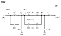
- FIG. 1 is an equivalent circuit diagram of a filter device according to a first embodiment.
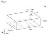
- 1 is an external perspective view of a filter device according to a first embodiment
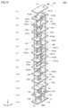
- FIG. 3 is an exploded perspective view showing an example of a laminated structure of the filter device of FIG. 2 .
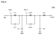
- FIG. 4 is an equivalent circuit diagram of a filter device of a comparative example.
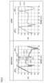
- 5A to 5C are diagrams for explaining filter characteristics of the filter devices of the first embodiment and the comparative example.
- FIG. 1 is a first diagram for explaining why spurious signals occur
- FIG. 2 is a second diagram for explaining why spurious signals occur
- 11A and 11B are diagrams for explaining filter characteristics when the line length of an inductor of a resonator is adjusted.
- FIG. 11 is an equivalent circuit diagram of a filter device according to a first modified example.
- FIG. 11 is an equivalent circuit diagram of a filter device according to a second modified example.
- FIG. 11 is an equivalent circuit diagram of a filter device according to a second embodiment.
- FIG. 11 is an exploded perspective view showing an example of a laminated structure of a filter device according to a second embodiment.
- FIG. 1 is a first diagram for explaining why the spurious level can be adjusted.
- FIG. 2 is a second diagram for explaining why the spurious level can be adjusted.
- 11 is a diagram for explaining the filter characteristics of the filter device of the second embodiment.
- FIG. FIG. 11 is an equivalent circuit diagram of a filter device according to a third modified example.
- FIG. 13 is an equivalent circuit diagram of a filter device according to a fourth modified example.
- FIG. 13 is an equivalent circuit diagram of a filter device according to a fifth modified example.
- FIG. 11 is an equivalent circuit diagram of a filter device according to a third embodiment. 13 is a diagram for explaining the filter characteristics of the filter device of the third embodiment.
- FIG. 11 is an equivalent circuit diagram of a filter device according to a fourth embodiment. 13 is a diagram for explaining the filter characteristics of a filter device according to a fourth embodiment.
- FIG. 13 is an equivalent circuit diagram of a filter device according to a sixth modified example. 13 is a diagram for explaining the filter characteristics of a filter device according to Modification 6.
- FIG. 11 is an equivalent circuit diagram of a filter device according to a third embodiment. 13 is a diagram for explaining the filter characteristics of the filter device of the third embodiment.
- FIG. FIG. 13 is an equivalent circuit diagram of a filter device
- [First embodiment] 1 is an equivalent circuit diagram of a filter device 100 according to a first embodiment.
- the filter device 100 includes an input terminal T1, an output terminal T2, a ground terminal GND, resonators RC0 and RC1, capacitors C1 and C2, and an inductor L31.
- the resonator RC0 includes an inductor L11 and a capacitor C11.
- the resonator RC1 includes capacitors C21 to C23, and inductors L21 and L22.
- the resonator RC0 is connected to the input terminal T1. More specifically, one end of the inductor L11 is connected to the input terminal T1, and the capacitor C11 is connected in parallel to the inductor L11.
- inductor L31 One end of inductor L31 is connected to output terminal T2.
- the other end of inductor L11 included in resonator RC0 is connected to terminal N1 (first terminal) of resonator RC1, and the other end of inductor L31 is connected to terminal N2 (second terminal) of resonator RC1.
- inductors L21 and L22 are connected in series between terminal N1, which is connected to inductor L11, and terminal N2, which is connected to inductor L31.
- One end of capacitor C21 is connected to terminal N1, and the other end is connected to one end of capacitor C22.
- the other end of capacitor C22 is connected to terminal N2. That is, the series-connected capacitors C21 and C22 are connected in parallel to the series-connected inductors L21 and L22.
- Capacitor C23 is connected between connection node N11 between inductor L21 and inductor L22, and connection node N12 between capacitor C21 and capacitor C22.
- Capacitor C1 is connected between terminal N1 of resonator RC1 and ground terminal GND.
- Capacitor C2 is connected between terminal N2 of resonator RC1 and ground terminal GND.
- filter device 100 constitutes a so-called fifth-order low-pass filter.
- connection includes not only the case where two elements are directly connected, but also the case where they are connected via another element.
- Figure 2 is an external perspective view of the filter device 100
- Figure 3 is an exploded perspective view showing an example of the layered structure of the filter device 100.
- the filter device 100 includes a rectangular or approximately rectangular laminate 110 in which a plurality of dielectric layers LY1 to LY14 are laminated in the lamination direction.
- the dielectric layers LY1 to LY14 are formed of ceramics, such as low temperature co-fired ceramics (LTCC), or resin.
- LTCC low temperature co-fired ceramics
- the inductor and capacitor described in FIG. 1 are formed by a plurality of electrodes provided on each dielectric layer and a plurality of vias provided between the dielectric layers.
- the term "via” refers to a columnar conductor provided in a dielectric layer to connect electrodes provided on different dielectric layers.
- the vias are formed, for example, by conductive paste, plating, and/or metal pins.
- the stacking direction of the dielectric layers LY1 to LY14 in the laminate 110 is referred to as the "Z-axis direction"
- the direction perpendicular to the Z-axis direction and along the long side of the laminate 110 is referred to as the "X-axis direction”
- the direction along the short side of the laminate 110 is referred to as the "Y-axis direction”.
- the positive direction of the Z-axis in each figure may be referred to as the upper side, and the negative direction as the lower side.
- a directional mark DM for identifying the orientation of the filter device 100 is arranged on the upper surface 111 (dielectric layer LY1) of the laminate 110.
- External terminals (input terminal T1, output terminal T2, and ground terminal GND) for connecting the filter device 100 to an external device are arranged on the lower surface 112 (dielectric layer LY14) of the laminate 110.
- Each of the input terminal T1, output terminal T2, and ground terminal GND is a flat electrode having a substantially rectangular shape, and is an LGA (Land Grid Array) terminal regularly arranged on the lower surface 112 of the laminate 110.
- the input terminal T1 is arranged along the short side of the lower surface 112 in the positive direction of the X-axis.
- the output terminal T2 is arranged along the short side of the lower surface 112 in the negative direction of the X-axis.
- the ground terminal GND is arranged between the input terminal T1 and the output terminal T2 in the X-axis direction.
- the input terminal T1 is connected by a via V10 to a plate electrode P1 arranged on the dielectric layer LY13.
- the plate electrode P1 is an electrode having a substantially L-shape when viewed in a plan view from the stacking direction (Z-axis direction).
- the plate electrode P1 is connected by a via V11 to a capacitor electrode PC10 arranged on the dielectric layer LY9, a capacitor electrode PC11 arranged on the dielectric layer LY7, and a plate electrode PL10 arranged on the dielectric layer LY2.
- the plate electrode PL10 arranged on the dielectric layer LY2 is a linear strip-shaped electrode extending in the Y-axis direction.
- a via V11 is connected to a first end of the plate electrode PL10, and a via V12 is connected to a second end.
- Via V13 is connected to plate electrode PL20 arranged on dielectric layer LY2. Via V13 is also connected to capacitor electrode PC22 arranged on dielectric layer LY7, capacitor electrode PC12 arranged on dielectric layer LY8, and capacitor electrode PC3 arranged on dielectric layer LY9.
- Capacitor electrode PC3 is connected to capacitor electrode PC1 arranged on dielectric layer LY11 through via V14. When viewed in a plan view from the stacking direction, at least a portion of capacitor electrode PC1 overlaps with ground electrode PG1 arranged on dielectric layer LY12. Ground electrode PG1 is connected to ground terminal GND on lower surface 112 through multiple vias VG1. That is, capacitor electrode PC1 and ground electrode PG1 form capacitor C1 in FIG. 1.
- inductor L11 in FIG. 1 is formed by a path (first path) that runs from input terminal T1 through vias V10 to V14, capacitor electrode PC3, and plate electrodes P1, PL10, and PL11 to capacitor electrode PC1.
- the plate electrode PL20 is an electrode that has a substantially L-shape when viewed in a plan view from the stacking direction.
- a via V13 is connected to a first end of the plate electrode PL20, and a via V20 is connected to a second end.
- the via V20 is connected to a capacitor electrode PC20 disposed on the dielectric layer LY5.
- a via V21 is also connected to the capacitor electrode PC20.
- the via V21 is connected to the plate electrode PL30 disposed on the dielectric layer LY2.
- the plate electrode PL30 is an electrode that has a substantially L-shape when viewed in a plan view from the stacking direction.
- a via V21 is connected to a first end of the plate electrode PL30, and a via V22 is connected to a second end.
- the via V22 is connected to the plate electrode PL31 arranged on the dielectric layer LY4, the capacitor electrode PC23 arranged on the dielectric layer LY7, and the capacitor electrode PC4 arranged on the dielectric layer LY9.
- Capacitor electrode PC4 is connected to capacitor electrode PC2 arranged on dielectric layer LY11 through via V23. When viewed in a plan view from the stacking direction, at least a portion of capacitor electrode PC2 overlaps with ground electrode PG1 arranged on dielectric layer LY12. In other words, capacitor electrode PC2 and ground electrode PG1 form capacitor C2 in FIG. 1.
- the plate electrode PL31 of the dielectric layer LY4 is an electrode having a substantially L-shape when viewed from above in the stacking direction.
- a via V21 is connected to a first end of the plate electrode PL31, and a via V30 is connected to a second end.
- the via V30 is connected to the plate electrode PL32 arranged on the dielectric layer LY3.
- the plate electrode PL32 is a linear strip-shaped electrode extending in the Y-axis direction.
- a via V30 is connected to a first end of the plate electrode PL32, and a via V31 is connected to a second end.
- the via V31 is connected to the output terminal T2 on the lower surface 112 via the plate electrode P4 arranged on the dielectric layer LY13 and the via V32.
- Inductor L31 in FIG. 2 is formed by the path (second path) from output terminal T2, via vias V22, V23, V30-V32, capacitor electrode PC4, and plate electrodes P4, PL31, and PL32, to capacitor electrode PC2.
- Inductor L21 in FIG. 2 is formed by the path from plate electrode PL11, via vias V13, V20, and plate electrode PL20, to capacitor electrode PC20.
- Inductor L22 in FIG. 2 is formed by the path from capacitor electrode PC20, via vias V21, V22, and plate electrode PL30, to plate electrode PL31.
- Capacitor C21 in FIG. 2 is formed by capacitor electrodes PC21, PC24 and capacitor electrodes PC22, PC3.
- Capacitor C22 in FIG. 2 is formed by capacitor electrodes PC21, PC24 and capacitor electrodes PC23, PC4.
- Capacitor C23 in FIG. 2 is formed by capacitor electrodes PC20 and capacitor electrodes PC21.
- FIG. 4 is an equivalent circuit diagram of the filter device 100X of the comparative example.
- the resonator RC1 in the filter device 100 is replaced with a resonator RC1X.
- the resonator RC1X has a configuration in which an inductor L21X and a capacitor C21X are connected in parallel. In other words, it corresponds to a configuration in which the capacitor C23 of the resonator RC1 in the filter device 100 of the first embodiment is removed.
- mobile communication devices such as smartphones and mobile phones have adopted configurations that use microwave frequency bands of 6 GHz or less, such as Wi-Fi, and millimeter wave frequency bands of 28 GHz and 39 GHz that correspond to the 5G communication standard.
- microwave frequency bands of 6 GHz or less such as Wi-Fi
- millimeter wave frequency bands of 28 GHz and 39 GHz that correspond to the 5G communication standard.
- spurious signals such as those described above occur in the millimeter wave band in a low-pass filter used in a circuit that processes microwave band radio waves, the attenuation characteristics of the millimeter wave band may deteriorate, generating noise in that frequency band and potentially leading to a deterioration in communication quality.
- a capacitor (capacitor C23 in FIG. 2) having a capacitance relatively larger than the stray capacitance is incorporated in advance into the resonator, thereby lowering the frequency of the spurious signals caused by the stray capacitance and causing the spurious signals to occur in the non-pass band between the two frequency bands of the target radio waves used for communication.
- FIG. 5 is a diagram for explaining the filter characteristics of the filter device 100 of the first embodiment and the filter device 100X of the comparative example.
- the left column of FIG. 5 shows the simulation results of the pass characteristics of the filter device 100 of the first embodiment, and the right column shows the simulation results of the pass characteristics of the filter device 100X of the comparative example.
- the horizontal axis indicates frequency
- the vertical axis indicates reflection loss (LN14 to LN17, LN19) and insertion loss (lines LN10 to LN13, LN18).
- the capacitance value of capacitor C23 is changed.
- the frequency band BW1 of signals targeted by filter device 100 of this embodiment 1 is, for example, in the microwave range of 0 to 6 GHz
- the frequency band BW2 of other signals within the communication device is in the millimeter wave range of 27.5 GHz to 40 GHz.
- the frequency at which the spurious signals occur is between the frequency bands BW1 and BW2 of the two signals (17 GHz to 24 GHz). This ensures the amount of attenuation in the millimeter wave frequency band BW2, and provides the desired attenuation characteristics.
- the magnitude of the spurious response varies depending on the structural asymmetry of resonator RC1. Specifically, in FIG. 1, if the resonant frequency of a resonator made up of inductor L21 and capacitor C21 differs from the resonant frequency of a resonator made up of inductor L22 and capacitor C22, the effect of the spurious response increases.
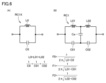
- FIG. 6 shows the left diagram (A) of Figure 6 shows the resonator RC1X portion of the comparative example, and the right diagram (B) shows the resonator RC1 portion of the filter device 100 of embodiment 1.
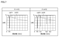
- Figure 7 shows the insertion loss (solid lines LN71, LN75) and reflection loss (wavy lines LN72, LN76) of resonator RC1.
- the inductance value of inductor L21X in resonator RC1X is L0, and the capacitance value of capacitor C21X is C0.
- the inductance values of inductors L21 and L22 in resonator RC1 are L01 and L02, respectively, and the capacitance values of capacitors C21 to C23 are C01, C02, and Ca, respectively.
- the resonant frequency F0 of the resonator RC1X can be expressed by the following equation (1).
- the spurious frequency fs changes. Specifically, as the stray capacitance Ca increases, the spurious frequency fs gradually decreases to fs3, fs2, and fs1, approaching the resonant frequency F0. Note that even if the stray capacitance Ca changes, the overall resonant frequency F0 remains almost unchanged.
- stray capacitance Generally, unintentionally occurring stray capacitance is small, so spurious emissions occur at relatively high frequencies.
- a capacitor C23 having a capacitance value larger than the stray capacitance Ca is pre-connected to the stray capacitance Ca, so that the effect of capacitor C23 on the frequency of the spurious emissions is more dominant than the unintentionally occurring stray capacitance.
- the capacitance value Ca of capacitor C23 it is possible to intentionally generate spurious emissions while adjusting the frequency of the spurious emissions.
- FIG. 8 is a diagram for explaining the filter characteristics when the resonant frequencies F1 and F2 described in FIG. 6 are adjusted by adjusting the line lengths of the inductors L21 and L22 of the resonator RC1 in the filter device 100.
- the solid lines LN20 and LN25 show the filter characteristics after the resonant frequencies F1 and F2 are adjusted to be approximately the same by adjusting the line lengths
- the dashed lines LN21 and LN26 show the filter characteristics before the line lengths are adjusted.
- the level of spurious noise occurring around 16 GHz is reduced by adjusting the resonant frequencies F1 and F2 to be approximately the same by adjusting the line lengths.
- the frequency at which spurious emissions occur can be intentionally adjusted by placing a capacitor between the middle part of the inductor of the resonator and the middle part of the capacitor. Furthermore, in this resonator, the length of the two inductors connected to the spurious emission adjustment capacitor can be adjusted to adjust the resonant frequencies F1 and F2 of the resonator formed on the input side and output side of the capacitor to be approximately the same, thereby reducing the level of spurious emissions.
- the “resonator RC1" in the first embodiment corresponds to the "first resonator” in this disclosure.
- the “inductor L21”, “inductor L22”, “inductor L11” and “inductor L31” in the first embodiment correspond to the "first inductor” to the "fourth inductor” in this disclosure, respectively.
- the “capacitor C21”, “capacitor C22” and “capacitor C23” in the first embodiment correspond to the “first capacitor” to the “third capacitor” in this disclosure, respectively.
- the “capacitor C1" and “capacitor C2" in the first embodiment correspond to the "fifth capacitor” and “sixth capacitor” in this disclosure.
- the “capacitor C11" in the first embodiment corresponds to the “seventh capacitor” in this disclosure.
- the "frequency band BW1" and “frequency band BW2" in the first embodiment correspond to the "first frequency band” and “second frequency band” in this disclosure, respectively.
- capacitor electrode PC22 corresponds to the "first capacitor electrode” to the "fourth capacitor electrode” in this disclosure, respectively.
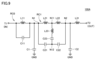
- FIG. 9 is an equivalent circuit diagram of filter device 100A of modified example 1.
- filter device 100A an inductor L23 is added to the capacitor C23 in the configuration of filter device 100 shown in FIG. 1. More specifically, inductor L23 is disposed between capacitor C23 and connection node N11 between inductor L21 and inductor L22. The rest of the configuration in FIG. 9 is the same as in FIG. 1, and descriptions of elements that overlap with FIG. 1 will not be repeated.
- the frequency of the generated spurious can be adjusted by adjusting the resonant frequency of the LC series resonator.
- the capacitance of the capacitor required for the frequency adjustment circuit can be reduced, allowing for a reduction in the size of the equipment.
- inductor L23 and capacitor C23 may be reversed. That is, capacitor C23 may be connected to connection node N11, and inductor L23 may be connected between capacitor C23 and connection node N12.
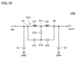
- FIG. 10 is an equivalent circuit diagram of a filter device 100B of modified example 2.
- the filter device 100B has a configuration in which the resonator RC0 and the inductor L31 in the filter device 100 shown in FIG. 1 have been removed.
- the filter device 100B is a third-order low-pass filter consisting of the resonator RC1 and the capacitors C1 and C2, which are shunt capacitors.
- a capacitor is provided that connects the center part of the inductor that constitutes the parallel resonator with the center part of the capacitor, and the capacitance of the capacitor is made larger than the stray capacitance to intentionally lower the frequency of the spurious emissions and prevent the spurious emissions from overlapping with the pass band of the high-frequency signal, thereby suppressing the deterioration of the attenuation characteristics of the non-pass band of the low-pass filter.
- FIG. 11 is an equivalent circuit diagram of a filter device 100C according to the second embodiment.
- a capacitor C25 is added between the ground terminal GND and the capacitor C23 for adjusting the spurious frequency in the resonator RC1 of the filter device 100 of the first embodiment.
- the description of the elements that overlap with the filter device 100 of FIG. 1 will not be repeated.
- a capacitor C25 is disposed between the connection node N11 between the inductors L21 and L22 and the ground terminal GND.
- capacitor C23 which is used for adjusting spurious components, relative to the ground potential can be determined by capacitor C25. Furthermore, after adjusting the frequency of the spurious components using capacitor C23, the anti-resonance frequency of the spurious components can be brought closer to the resonance frequency by adjusting the size of capacitor C25, so that the anti-resonance point and the resonance point cancel each other out, thereby reducing the level of the spurious components.
- the via V20C is connected to the plate electrode PL20 of the dielectric layer LY2 and the capacitor electrode PC20 of the dielectric layer LY5, as well as to the capacitor electrode PC25 arranged on the dielectric layer LY10.
- the via V21C is connected to the plate electrode PL30 of the dielectric layer LY2 and the capacitor electrode PC20 of the dielectric layer LY5, as well as to the capacitor electrode PC26 arranged on the dielectric layer LY10.
- Each of the capacitor electrodes PC25, PC26 is a band-shaped electrode extending in the X-axis direction, and at least a portion of each electrode overlaps with the ground electrode PG1 of the dielectric layer LY12 when viewed in a plan view from the stacking direction. That is, the capacitor electrodes PC25, PC26 and the ground electrode PG1 form the capacitor C25 in FIG. 11.
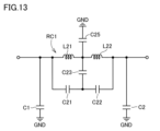
- Figure 13 shows the resonator RC1 and capacitors C1 and C2 in the filter device 100C shown in Figure 11.
- Figure 13 is a low-pass filter in which resonator RC0 and inductor L31 have been removed from filter device 100C.
- Figure 14 shows the simulation results of the insertion loss (solid lines LN81, LN83, LN85) and reflection loss (dashed lines LN82, LN84, LN86) when the capacitance value Cb of capacitor C25 is changed in the filter of Figure 13.
- the center diagram in Figure 14 shows the case where the capacitance value Cb of capacitor C25 is close to a specific capacitance value Copt (Cb ⁇ Copt).
- the left diagram shows the case where the capacitance value Cb is greater than the capacitance value Copt (Cb > Copt), and the right diagram shows the case where the capacitance value Cb is less than the capacitance value Copt (Cb ⁇ Copt).
- the capacitance value Copt is the capacitance value when the resonance point that causes the spurious and the anti-resonance point coincide.
- the amplitude at the anti-resonance point that inhibits attenuation is offset by the amplitude at the resonance point, reducing the spurious level.
- FIG. 15 is a diagram for explaining the filter characteristics of the filter device 100C of the second embodiment.
- the solid line LN30 indicates the insertion loss
- the dashed line LN35 indicates the reflection loss.
- the spurious level increases whether the capacitance value is greater or smaller than this optimal value.
- the capacitance value is greater than the optimal value, the spurious resonance point and anti-resonance point appear in this order from the low frequency side to the high frequency side.
- the capacitance value is smaller than the optimal value, the spurious anti-resonance point and resonance point appear in this order from the low frequency side to the high frequency side. Then, by setting the capacitance value of capacitor C25 so that the resonance point and anti-resonance point of the generated spurious are close to each other, the spurious level can be reduced by canceling out the anti-resonance point and the resonance point.
- the level of spurious signals generated can be reduced.
- Capacitor C25 in embodiment 2 corresponds to an example of a “fourth capacitor” in this disclosure.
- Capacitor electrode PC25 and “capacitor electrode PC26” in embodiment 2 correspond to a “fifth capacitor electrode” and a “sixth capacitor electrode” in this disclosure, respectively.
- FIG. 16 is an equivalent circuit diagram of a filter device 100D of the third modification.
- a capacitor C26 is added between the capacitor C23 in the resonator RC1 of the filter device 100 and the ground terminal GND. More specifically, the capacitor C26 is disposed between the connection node N12 between the capacitors C21 and C22 and the ground terminal GND.
- Capacitor C26 in variant example 3 corresponds to an example of a “fourth capacitor” in this disclosure.
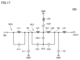
- FIG. 17 is an equivalent circuit diagram of a filter device 100E of the fourth modified example.
- an inductor L25 is added to the filter device 100C of the second embodiment described in FIG. 11. More specifically, the inductor L25 is disposed between the capacitor C25 and the ground terminal GND. The capacitor C25 and the inductor L25 form an LC series resonator.
- the anti-resonance frequency of the spurious can be brought closer to the resonance frequency, and the anti-resonance point and the resonance point cancel each other out, reducing the spurious level.
- inductor L25 and capacitor C25 in the LC series resonator may be reversed.
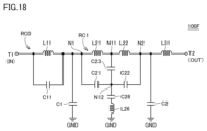
- FIG. 18 is an equivalent circuit diagram of a filter device 100F of modified example 5.
- an inductor L26 is added to the filter device 100D of modified example 3 described in FIG. 16. More specifically, the inductor L26 is disposed between the capacitor C26 and the ground terminal GND. The capacitor C26 and the inductor L26 form an LC series resonator.
- the anti-resonance frequency of the spurious can be brought closer to the resonance frequency. This causes the anti-resonance point and the resonance point to cancel each other out, reducing the spurious level.
- inductor L26 and capacitor C26 in the LC series resonator may be reversed.
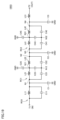
- FIG. 19 is an equivalent circuit diagram of a filter device 100G according to the third embodiment.
- the filter device 100G has a configuration in which a resonator RC2 having a configuration similar to that of the resonator RC1, a capacitor C45 for adjusting the spurious level, and a shunt capacitor C3 are added to the filter device 100C according to the second embodiment shown in FIG. 11.
- a resonator RC2 is connected between the terminal N2 of the resonator RC1 and the inductor L31.
- the resonator RC2 includes inductors L41 and L42 and capacitors C41 to C43.
- inductors L41 and L42 are connected in series between terminal N3 (third terminal) connected to terminal N2 of resonator RC1 and terminal N4 (fourth terminal) connected to inductor L31.
- One end of capacitor C41 is connected to terminal N3, and the other end is connected to one end of capacitor C42.
- the other end of capacitor C42 is connected to terminal N4. That is, the series-connected capacitors C41 and C42 are connected in parallel to the series-connected inductors L41 and L42.
- a capacitor C43 for adjusting the spurious frequency is connected between a connection node N31 between inductor L41 and inductor L42 and a connection node N32 between capacitor C41 and capacitor C42.
- a capacitor C45 for adjusting the spurious level is connected between the connection node N31 between the inductors L41 and L42 and the ground terminal GND. Furthermore, a capacitor C3 is connected between the terminal N4 and the ground terminal GND.
- the filter device 100G forms a seventh-order low-pass filter.
- the capacitors C43 and C45 can reduce the frequency and level of the spurious generated by the inductor of the resonator RC2, improving the attenuation characteristics of the low-pass filter.
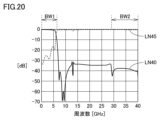
- FIG. 20 is a diagram for explaining the filter characteristics of the filter device 100G of the third embodiment.
- the horizontal axis indicates frequency
- the vertical axis indicates insertion loss (solid line LN40) and reflection loss (dashed line LN45).
- solid line LN40 insertion loss
- LN45 reflection loss
- spurious signals occur near 13 GHz between the microwave frequency band BW1 and the millimeter wave frequency band BW2.
- the attenuation characteristics in the non-pass band above 13 GHz are almost flat with an attenuation of 30 dB or more.
- the capacitors C43 and C45 may be replaced with an LC series resonator as shown in FIG. 9. Also, as shown in FIG. 16 or 18, a capacitor or an LC series resonator may be disposed between the connection node N32 between the capacitors C41 and C42 and the ground terminal GND.
- the “resonator RC2" in the third embodiment corresponds to the "second resonator” in this disclosure.
- the “capacitor C3,” “capacitor C41,” “capacitor C42,” and “capacitor C43” in the third embodiment correspond to the "eighth capacitor to eleventh capacitor,” respectively, in this disclosure.
- the “inductor L41” and “inductor L42” in the third embodiment correspond to the "fifth inductor” and “sixth inductor,” respectively, in this disclosure.
- the filter device is a low-pass filter.
- a fourth embodiment a configuration in which the features of the present disclosure are applied to a third- or higher-order band-pass filter using an LC parallel resonator will be described.
- FIG. 21 is an equivalent circuit diagram of a filter device 100H according to embodiment 4.
- the capacitors C1 and C2 in the third-order low-pass filter device 100B shown in FIG. 10 are replaced with resonators RC3 and RC4, respectively.
- the resonator RC3 includes an inductor L51 and a capacitor C51 connected in parallel between the terminal N1 of the resonator RC1 and the ground terminal GND.
- the resonator RC4 includes an inductor L52 and a capacitor C52 connected in parallel between the terminal N2 of the resonator RC1 and the ground terminal GND.
- the resonators RC3 and RC4 form an LC parallel resonator, and the filter device 100H functions as a third-order bandpass filter.
- FIG. 22 is a diagram for explaining the filter characteristics of the filter device 100H of embodiment 4.
- FIG. 22 also shows the insertion loss (dashed line LN51) and reflection loss (dashed line LN56) in a comparative example having a configuration without the capacitor C23 in FIG. 21.
- spurious signals that occurred near 31 GHz in the millimeter wave frequency band BW2 have shifted to near 8 GHz in the filter device 100H. This reduces the effect on the millimeter wave frequency band BW2.
- the spurious frequency generated by the inductor of resonator RC1 can be adjusted by capacitor C23 included in resonator RC1 to a frequency that does not affect the passband of other signals. Therefore, it is possible to suppress the deterioration of the attenuation characteristics of the bandpass filter.
- the "resonator RC3" and “resonator RC4" in the fourth embodiment correspond to the "third resonator” and “fourth resonator” in this disclosure, respectively.
- the “inductor L51” and “inductor L52” in the fourth embodiment correspond to the “seventh inductor” and “eighth inductor” in this disclosure, respectively.
- the “capacitor C51” and “capacitor C52” in the fourth embodiment correspond to the “twelfth capacitor” and “thirteenth capacitor” in this disclosure, respectively.
- FIG. 23 is an equivalent circuit diagram of a filter device 100I of modified example 6.
- an LC series resonator composed of an inductor L25 and a capacitor C25 is disposed between a connection node N11 between inductors L21 and L22 in resonator RC1 and a ground terminal GND.
- FIG. 24 is a diagram for explaining the filter characteristics of the filter device 100I of the sixth modified example.
- the insertion loss (solid line LN60) and reflection characteristics (dashed line LN65) of the filter device 100I are shown.
- a filter device includes an input terminal, an output terminal, and a first resonator connected to the input terminal and the output terminal.
- the first resonator includes a first terminal connected to the input terminal, a second terminal connected to the output terminal, a first inductor and a second inductor, and a first to a third capacitor.
- One end of the first inductor is connected to the first terminal.
- One end of the second inductor is connected to the second terminal, and the other end is connected to the other end of the first inductor.
- One end of the first capacitor is connected to the first terminal.
- One end of the second capacitor is connected to the second terminal, and the other end is connected to the other end of the first capacitor.
- the third capacitor is connected between the other end of the first inductor and the other end of the first capacitor.
- the filter device described in 1 further includes a fourth capacitor connected between the third capacitor and the ground terminal.
- the fourth capacitor is connected between the other end of the first inductor and the ground terminal.
- the fourth capacitor is connected between the other end of the first capacitor and the ground terminal.
- the filter device described in any one of 1 to 4 further includes a ground terminal, a fifth capacitor connected between the first terminal and the ground terminal, and a sixth capacitor connected between the second terminal and the ground terminal.
- the filter device has a first frequency band as a pass band and a frequency band higher than the first frequency band as a non-pass band.
- the third capacitor generates spurious signals in a frequency band between the first frequency band and a second frequency band included in the non-pass band.
- the filter device described in 5 further includes a third inductor connected between the input terminal and the first terminal, a seventh capacitor connected in parallel to the third inductor, and a fourth inductor connected between the output terminal and the second terminal.
- the filter device described in Item 7 further includes a second resonator connected between the second terminal and the fourth inductor, and an eighth capacitor connected between a connection node of the second resonator and the fourth inductor and a ground terminal.
- the second resonator includes a third terminal connected to the second terminal, a fourth terminal connected to the fourth inductor, a fifth inductor and a sixth inductor, and ninth to eleventh capacitors.
- One end of the fifth inductor is connected to the third terminal.
- One end of the sixth inductor is connected to the fourth inductor, and the other end is connected to the other end of the fifth inductor.
- One end of the ninth capacitor is connected to the third terminal.
- One end of the tenth capacitor is connected to the fourth inductor, and the other end is connected to the other end of the fifth capacitor.
- the eleventh capacitor is connected between the other end of the fifth inductor and the other end of the ninth capacitor.
- the filter device described in any one of clauses 1 to 4 further includes a ground terminal, a third resonator connected between the first terminal and the ground terminal, and a fourth resonator connected between the second terminal and the ground terminal.
- the third resonator includes a seventh inductor connected between the first terminal and the ground terminal, and a twelfth capacitor connected in parallel to the seventh inductor.
- the fourth resonator includes an eighth inductor connected between the second terminal and the ground terminal, and a thirteenth capacitor connected in parallel to the eighth inductor.
- a filter device includes a laminate in which a plurality of dielectrics are stacked, an input terminal, an output terminal, a ground terminal, a first path and a second path, and a first to fourth capacitor electrodes.
- the first path is connected to the input terminal.
- the second path is connected to the output terminal.
- the first capacitor electrode is connected to the first path.
- the second capacitor electrode is connected to the second path.
- the third capacitor electrode is connected to the first path and the second path.
- the first capacitor electrode and the second capacitor electrode are arranged on the same dielectric layer.
- the fourth capacitor electrode is arranged on a dielectric layer between the dielectric layer on which the first capacitor electrode and the second capacitor electrode are arranged and the dielectric layer on which the third capacitor electrode is arranged.
- the filter device described in 10 or 11 further includes a ground electrode connected to the ground terminal, and a fifth capacitor electrode and a sixth capacitor electrode connected to the third capacitor electrode. When viewed in a plan view from the stacking direction of the laminate, at least a portion of the fifth capacitor electrode and at least a portion of the sixth capacitor electrode overlap the ground electrode.
Landscapes
- Engineering & Computer Science (AREA)
- Power Engineering (AREA)
- Filters And Equalizers (AREA)
Priority Applications (3)
| Application Number | Priority Date | Filing Date | Title |
|---|---|---|---|
| JP2025508380A JPWO2024195697A1 (cg-RX-API-DMAC7.html) | 2023-03-20 | 2024-03-14 | |
| US19/332,135 US20260019058A1 (en) | 2023-03-20 | 2025-09-18 | Filter device and method for controlling a filter device |
| JP2026000828A JP2026053722A (ja) | 2023-03-20 | 2026-01-06 | フィルタ装置 |
Applications Claiming Priority (2)
| Application Number | Priority Date | Filing Date | Title |
|---|---|---|---|
| JP2023044202 | 2023-03-20 | ||
| JP2023-044202 | 2023-03-20 |
Related Child Applications (1)
| Application Number | Title | Priority Date | Filing Date |
|---|---|---|---|
| US19/332,135 Continuation US20260019058A1 (en) | 2023-03-20 | 2025-09-18 | Filter device and method for controlling a filter device |
Publications (1)
| Publication Number | Publication Date |
|---|---|
| WO2024195697A1 true WO2024195697A1 (ja) | 2024-09-26 |
Family
ID=92841484
Family Applications (1)
| Application Number | Title | Priority Date | Filing Date |
|---|---|---|---|
| PCT/JP2024/010093 Ceased WO2024195697A1 (ja) | 2023-03-20 | 2024-03-14 | フィルタ装置 |
Country Status (3)
| Country | Link |
|---|---|
| US (1) | US20260019058A1 (cg-RX-API-DMAC7.html) |
| JP (2) | JPWO2024195697A1 (cg-RX-API-DMAC7.html) |
| WO (1) | WO2024195697A1 (cg-RX-API-DMAC7.html) |
Citations (2)
| Publication number | Priority date | Publication date | Assignee | Title |
|---|---|---|---|---|
| JP2002204136A (ja) * | 2000-12-28 | 2002-07-19 | Soshin Electric Co Ltd | 積層型ローパスフィルタ |
| JP2004343696A (ja) * | 2003-02-20 | 2004-12-02 | Tdk Corp | フィルタ回路網およびその設計方法ならびにマルチバンド送信機 |
Family Cites Families (2)
| Publication number | Priority date | Publication date | Assignee | Title |
|---|---|---|---|---|
| JP6664257B2 (ja) * | 2016-03-30 | 2020-03-13 | 太陽誘電株式会社 | ローパスフィルター |
| CN115461931B (zh) * | 2020-05-25 | 2024-06-04 | 株式会社村田制作所 | Lc滤波器以及使用该lc滤波器的双工器和复用器 |
-
2024
- 2024-03-14 JP JP2025508380A patent/JPWO2024195697A1/ja active Pending
- 2024-03-14 WO PCT/JP2024/010093 patent/WO2024195697A1/ja not_active Ceased
-
2025
- 2025-09-18 US US19/332,135 patent/US20260019058A1/en active Pending
-
2026
- 2026-01-06 JP JP2026000828A patent/JP2026053722A/ja active Pending
Patent Citations (2)
| Publication number | Priority date | Publication date | Assignee | Title |
|---|---|---|---|---|
| JP2002204136A (ja) * | 2000-12-28 | 2002-07-19 | Soshin Electric Co Ltd | 積層型ローパスフィルタ |
| JP2004343696A (ja) * | 2003-02-20 | 2004-12-02 | Tdk Corp | フィルタ回路網およびその設計方法ならびにマルチバンド送信機 |
Also Published As
| Publication number | Publication date |
|---|---|
| US20260019058A1 (en) | 2026-01-15 |
| JP2026053722A (ja) | 2026-03-25 |
| JPWO2024195697A1 (cg-RX-API-DMAC7.html) | 2024-09-26 |
Similar Documents
| Publication | Publication Date | Title |
|---|---|---|
| JP4579198B2 (ja) | 多層帯域通過フィルタ | |
| US8018299B2 (en) | Band-pass filter circuit and multi-layer structure and method thereof | |
| US7423500B2 (en) | Low-pass filter capable of preventing unnecessary electromagnetic coupling | |
| US7432786B2 (en) | High frequency filter | |
| US9882542B2 (en) | Filter component | |
| WO2016042990A1 (ja) | 高周波部品 | |
| US12451855B2 (en) | Filter device and radio-frequency front-end circuit including the same | |
| US11190161B2 (en) | Filter device | |
| US12244285B2 (en) | LC filter, and diplexer and multiplexer using same | |
| JPWO2013069498A1 (ja) | Lcフィルタ回路及び高周波モジュール | |
| US12107312B2 (en) | Band pass filter and high frequency front-end circuit including same | |
| JP2011147090A (ja) | 積層型マルチプレクサ、積層型トリプレクサ及びフィルタ回路 | |
| US20250330137A1 (en) | Filter device | |
| US12603664B2 (en) | Filter apparatus and radio-frequency front end circuit including the same | |
| US12586879B2 (en) | Dielectric resonator, and dielectric filter and multiplexer using same | |
| US12407319B2 (en) | Filter device and radio-frequency front-end circuit including the same | |
| JP2026053722A (ja) | フィルタ装置 | |
| WO2023281942A1 (ja) | フィルタ装置および高周波フロントエンド回路 | |
| JP2024113870A (ja) | フィルタ装置 | |
| JP7568070B2 (ja) | フィルタ装置およびそれを備えた高周波フロントエンド回路 | |
| JP2021072563A (ja) | マルチプレクサ | |
| US20260025118A1 (en) | Filter device and radio-frequency front-end circuit | |
| JP2009267811A (ja) | バンドパスフィルタ及び積層型バンドパスフィルタ。 | |
| WO2022209122A1 (ja) | 誘電体フィルタ | |
| WO2024247534A1 (ja) | フィルタ回路およびフィルタ装置 |
Legal Events
| Date | Code | Title | Description |
|---|---|---|---|
| 121 | Ep: the epo has been informed by wipo that ep was designated in this application |
Ref document number: 24774835 Country of ref document: EP Kind code of ref document: A1 |
|
| ENP | Entry into the national phase |
Ref document number: 2025508380 Country of ref document: JP Kind code of ref document: A |
|
| WWE | Wipo information: entry into national phase |
Ref document number: 2025508380 Country of ref document: JP |
|
| NENP | Non-entry into the national phase |
Ref country code: DE |
|
| 122 | Ep: pct application non-entry in european phase |
Ref document number: 24774835 Country of ref document: EP Kind code of ref document: A1 |