WO2024190847A1 - 光学積層体、画像表示パネル、及び画像表示装置 - Google Patents
光学積層体、画像表示パネル、及び画像表示装置 Download PDFInfo
- Publication number
- WO2024190847A1 WO2024190847A1 PCT/JP2024/009899 JP2024009899W WO2024190847A1 WO 2024190847 A1 WO2024190847 A1 WO 2024190847A1 JP 2024009899 W JP2024009899 W JP 2024009899W WO 2024190847 A1 WO2024190847 A1 WO 2024190847A1
- Authority
- WO
- WIPO (PCT)
- Prior art keywords
- weight
- less
- optical laminate
- meth
- polymer
- Prior art date
- Legal status (The legal status is an assumption and is not a legal conclusion. Google has not performed a legal analysis and makes no representation as to the accuracy of the status listed.)
- Ceased
Links
Images

Classifications
-
- C—CHEMISTRY; METALLURGY
- C09—DYES; PAINTS; POLISHES; NATURAL RESINS; ADHESIVES; COMPOSITIONS NOT OTHERWISE PROVIDED FOR; APPLICATIONS OF MATERIALS NOT OTHERWISE PROVIDED FOR
- C09J—ADHESIVES; NON-MECHANICAL ASPECTS OF ADHESIVE PROCESSES IN GENERAL; ADHESIVE PROCESSES NOT PROVIDED FOR ELSEWHERE; USE OF MATERIALS AS ADHESIVES
- C09J7/00—Adhesives in the form of films or foils
- C09J7/30—Adhesives in the form of films or foils characterised by the adhesive composition
- C09J7/38—Pressure-sensitive adhesives [PSA]
- C09J7/381—Pressure-sensitive adhesives [PSA] based on macromolecular compounds obtained by reactions involving only carbon-to-carbon unsaturated bonds
- C09J7/385—Acrylic polymers
-
- B—PERFORMING OPERATIONS; TRANSPORTING
- B32—LAYERED PRODUCTS
- B32B—LAYERED PRODUCTS, i.e. PRODUCTS BUILT-UP OF STRATA OF FLAT OR NON-FLAT, e.g. CELLULAR OR HONEYCOMB, FORM
- B32B27/00—Layered products comprising a layer of synthetic resin
-
- B—PERFORMING OPERATIONS; TRANSPORTING
- B32—LAYERED PRODUCTS
- B32B—LAYERED PRODUCTS, i.e. PRODUCTS BUILT-UP OF STRATA OF FLAT OR NON-FLAT, e.g. CELLULAR OR HONEYCOMB, FORM
- B32B27/00—Layered products comprising a layer of synthetic resin
- B32B27/18—Layered products comprising a layer of synthetic resin characterised by the use of special additives
-
- B—PERFORMING OPERATIONS; TRANSPORTING
- B32—LAYERED PRODUCTS
- B32B—LAYERED PRODUCTS, i.e. PRODUCTS BUILT-UP OF STRATA OF FLAT OR NON-FLAT, e.g. CELLULAR OR HONEYCOMB, FORM
- B32B7/00—Layered products characterised by the relation between layers; Layered products characterised by the relative orientation of features between layers, or by the relative values of a measurable parameter between layers, i.e. products comprising layers having different physical, chemical or physicochemical properties; Layered products characterised by the interconnection of layers
- B32B7/02—Physical, chemical or physicochemical properties
- B32B7/023—Optical properties
-
- B—PERFORMING OPERATIONS; TRANSPORTING
- B32—LAYERED PRODUCTS
- B32B—LAYERED PRODUCTS, i.e. PRODUCTS BUILT-UP OF STRATA OF FLAT OR NON-FLAT, e.g. CELLULAR OR HONEYCOMB, FORM
- B32B7/00—Layered products characterised by the relation between layers; Layered products characterised by the relative orientation of features between layers, or by the relative values of a measurable parameter between layers, i.e. products comprising layers having different physical, chemical or physicochemical properties; Layered products characterised by the interconnection of layers
- B32B7/02—Physical, chemical or physicochemical properties
- B32B7/025—Electric or magnetic properties
-
- C—CHEMISTRY; METALLURGY
- C09—DYES; PAINTS; POLISHES; NATURAL RESINS; ADHESIVES; COMPOSITIONS NOT OTHERWISE PROVIDED FOR; APPLICATIONS OF MATERIALS NOT OTHERWISE PROVIDED FOR
- C09J—ADHESIVES; NON-MECHANICAL ASPECTS OF ADHESIVE PROCESSES IN GENERAL; ADHESIVE PROCESSES NOT PROVIDED FOR ELSEWHERE; USE OF MATERIALS AS ADHESIVES
- C09J11/00—Features of adhesives not provided for in group C09J9/00, e.g. additives
- C09J11/02—Non-macromolecular additives
- C09J11/06—Non-macromolecular additives organic
-
- C—CHEMISTRY; METALLURGY
- C09—DYES; PAINTS; POLISHES; NATURAL RESINS; ADHESIVES; COMPOSITIONS NOT OTHERWISE PROVIDED FOR; APPLICATIONS OF MATERIALS NOT OTHERWISE PROVIDED FOR
- C09J—ADHESIVES; NON-MECHANICAL ASPECTS OF ADHESIVE PROCESSES IN GENERAL; ADHESIVE PROCESSES NOT PROVIDED FOR ELSEWHERE; USE OF MATERIALS AS ADHESIVES
- C09J133/00—Adhesives based on homopolymers or copolymers of compounds having one or more unsaturated aliphatic radicals, each having only one carbon-to-carbon double bond, and at least one being terminated by only one carboxyl radical, or of salts, anhydrides, esters, amides, imides, or nitriles thereof; Adhesives based on derivatives of such polymers
- C09J133/04—Homopolymers or copolymers of esters
- C09J133/14—Homopolymers or copolymers of esters of esters containing halogen, nitrogen, sulfur or oxygen atoms in addition to the carboxy oxygen
-
- C—CHEMISTRY; METALLURGY
- C09—DYES; PAINTS; POLISHES; NATURAL RESINS; ADHESIVES; COMPOSITIONS NOT OTHERWISE PROVIDED FOR; APPLICATIONS OF MATERIALS NOT OTHERWISE PROVIDED FOR
- C09J—ADHESIVES; NON-MECHANICAL ASPECTS OF ADHESIVE PROCESSES IN GENERAL; ADHESIVE PROCESSES NOT PROVIDED FOR ELSEWHERE; USE OF MATERIALS AS ADHESIVES
- C09J7/00—Adhesives in the form of films or foils
- C09J7/20—Adhesives in the form of films or foils characterised by their carriers
- C09J7/29—Laminated material
-
- C—CHEMISTRY; METALLURGY
- C09—DYES; PAINTS; POLISHES; NATURAL RESINS; ADHESIVES; COMPOSITIONS NOT OTHERWISE PROVIDED FOR; APPLICATIONS OF MATERIALS NOT OTHERWISE PROVIDED FOR
- C09J—ADHESIVES; NON-MECHANICAL ASPECTS OF ADHESIVE PROCESSES IN GENERAL; ADHESIVE PROCESSES NOT PROVIDED FOR ELSEWHERE; USE OF MATERIALS AS ADHESIVES
- C09J7/00—Adhesives in the form of films or foils
- C09J7/30—Adhesives in the form of films or foils characterised by the adhesive composition
- C09J7/38—Pressure-sensitive adhesives [PSA]
-
- C—CHEMISTRY; METALLURGY
- C09—DYES; PAINTS; POLISHES; NATURAL RESINS; ADHESIVES; COMPOSITIONS NOT OTHERWISE PROVIDED FOR; APPLICATIONS OF MATERIALS NOT OTHERWISE PROVIDED FOR
- C09J—ADHESIVES; NON-MECHANICAL ASPECTS OF ADHESIVE PROCESSES IN GENERAL; ADHESIVE PROCESSES NOT PROVIDED FOR ELSEWHERE; USE OF MATERIALS AS ADHESIVES
- C09J9/00—Adhesives characterised by their physical nature or the effects produced, e.g. glue sticks
- C09J9/02—Electrically-conducting adhesives
-
- G—PHYSICS
- G02—OPTICS
- G02B—OPTICAL ELEMENTS, SYSTEMS OR APPARATUS
- G02B1/00—Optical elements characterised by the material of which they are made; Optical coatings for optical elements
- G02B1/10—Optical coatings produced by application to, or surface treatment of, optical elements
- G02B1/14—Protective coatings, e.g. hard coatings
-
- G—PHYSICS
- G02—OPTICS
- G02B—OPTICAL ELEMENTS, SYSTEMS OR APPARATUS
- G02B1/00—Optical elements characterised by the material of which they are made; Optical coatings for optical elements
- G02B1/10—Optical coatings produced by application to, or surface treatment of, optical elements
- G02B1/16—Optical coatings produced by application to, or surface treatment of, optical elements having an anti-static effect, e.g. electrically conducting coatings
-
- G—PHYSICS
- G02—OPTICS
- G02B—OPTICAL ELEMENTS, SYSTEMS OR APPARATUS
- G02B5/00—Optical elements other than lenses
- G02B5/30—Polarising elements
-
- G—PHYSICS
- G02—OPTICS
- G02F—OPTICAL DEVICES OR ARRANGEMENTS FOR THE CONTROL OF LIGHT BY MODIFICATION OF THE OPTICAL PROPERTIES OF THE MEDIA OF THE ELEMENTS INVOLVED THEREIN; NON-LINEAR OPTICS; FREQUENCY-CHANGING OF LIGHT; OPTICAL LOGIC ELEMENTS; OPTICAL ANALOGUE/DIGITAL CONVERTERS
- G02F1/00—Devices or arrangements for the control of the intensity, colour, phase, polarisation or direction of light arriving from an independent light source, e.g. switching, gating or modulating; Non-linear optics
- G02F1/01—Devices or arrangements for the control of the intensity, colour, phase, polarisation or direction of light arriving from an independent light source, e.g. switching, gating or modulating; Non-linear optics for the control of the intensity, phase, polarisation or colour
- G02F1/13—Devices or arrangements for the control of the intensity, colour, phase, polarisation or direction of light arriving from an independent light source, e.g. switching, gating or modulating; Non-linear optics for the control of the intensity, phase, polarisation or colour based on liquid crystals, e.g. single liquid crystal display cells
- G02F1/133—Constructional arrangements; Operation of liquid crystal cells; Circuit arrangements
- G02F1/1333—Constructional arrangements; Manufacturing methods
- G02F1/1335—Structural association of cells with optical devices, e.g. polarisers or reflectors
- G02F1/13363—Birefringent elements, e.g. for optical compensation
-
- G—PHYSICS
- G09—EDUCATION; CRYPTOGRAPHY; DISPLAY; ADVERTISING; SEALS
- G09F—DISPLAYING; ADVERTISING; SIGNS; LABELS OR NAME-PLATES; SEALS
- G09F9/00—Indicating arrangements for variable information in which the information is built-up on a support by selection or combination of individual elements
-
- H—ELECTRICITY
- H10—SEMICONDUCTOR DEVICES; ELECTRIC SOLID-STATE DEVICES NOT OTHERWISE PROVIDED FOR
- H10K—ORGANIC ELECTRIC SOLID-STATE DEVICES
- H10K50/00—Organic light-emitting devices
- H10K50/80—Constructional details
- H10K50/86—Arrangements for improving contrast, e.g. preventing reflection of ambient light
-
- H—ELECTRICITY
- H10—SEMICONDUCTOR DEVICES; ELECTRIC SOLID-STATE DEVICES NOT OTHERWISE PROVIDED FOR
- H10K—ORGANIC ELECTRIC SOLID-STATE DEVICES
- H10K59/00—Integrated devices, or assemblies of multiple devices, comprising at least one organic light-emitting element covered by group H10K50/00
- H10K59/10—OLED displays
Definitions
- the present invention relates to an optical laminate, an image display panel, and an image display device.
- image display devices such as liquid crystal display devices and electroluminescence (EL) display devices (e.g., organic EL display devices, inorganic EL display devices) have rapidly become popular.
- EL electroluminescence
- image display devices have a layered structure of an image display cell, such as a liquid crystal cell or an EL light-emitting element, and an optical laminate including a polarizing plate and an adhesive sheet.
- the adhesive sheet is mainly used to bond between films included in the optical laminate, and to bond the image display cell to the optical laminate.
- static electricity is generated during their manufacture, for example when the optical laminate is attached to the image display cell via an adhesive sheet, or during use, for example when a user touches the image display device. If the image display device becomes charged with this static electricity, problems such as display defects can occur.
- Patent Documents 1 and 2 disclose a laminated structure that includes a polarizing film and a conductive layer that contains a conductive polymer.
- an object of the present invention is to provide an optical laminate that is more suitable for suppressing display defects.
- image display devices are prone to display defects in low-temperature environments, and based on this discovery, they completed the present invention.
- the present invention relates to An optical laminate comprising an adhesive sheet, an antistatic layer, and an optical film, the pressure-sensitive adhesive sheet is formed from a pressure-sensitive adhesive composition containing a polymer (A) and an antistatic agent,
- the optical laminate has a surface resistivity of 1.0 ⁇ 10 10 ⁇ / ⁇ or less at ⁇ 15° C. on the pressure-sensitive adhesive sheet side.
- an image display panel including the above optical laminate.
- the present invention relates to The present invention provides an image display device including the above image display panel.
- the present invention provides an optical laminate that is more suitable for suppressing display defects in low-temperature environments.
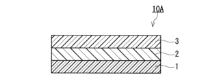
- FIG. 1 is a cross-sectional view that illustrates an example of an optical laminate according to this embodiment.
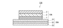
- FIG. 2 is a cross-sectional view that illustrates another example of the optical laminate according to this embodiment.
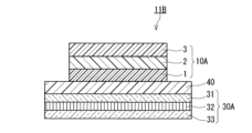
- FIG. 3 is a cross-sectional view that illustrates an example of an image display panel according to the present embodiment.
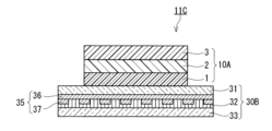
- FIG. 4 is a cross-sectional view that illustrates another example of the image display panel according to the present embodiment.
- FIG. 5 is a cross-sectional view that illustrates another example of the image display panel according to the present embodiment.
- the optical laminate according to the first aspect of the present invention is An optical laminate comprising an adhesive sheet, an antistatic layer, and an optical film, the pressure-sensitive adhesive sheet is formed from a pressure-sensitive adhesive composition containing a polymer (A) and an antistatic agent,
- the pressure-sensitive adhesive sheet side of the optical laminate has a surface resistivity of 1.0 ⁇ 10 10 ⁇ / ⁇ or less at ⁇ 15° C.
- the surface resistivity of the antistatic layer at 25° C. is 3.0 ⁇ 10 8 ⁇ / ⁇ or less.
- the surface resistivity of the antistatic layer at 25° C. is 1.0 ⁇ 10 7 ⁇ / ⁇ or more and 1.0 ⁇ 10 8 ⁇ / ⁇ or less.
- the polymer (A) is a (meth)acrylic polymer.
- the polymer (A) has a polyether structure.
- the polymer (A) has a constituent unit derived from a monomer shown in the following formula (1).
- R 1 is a hydrogen atom or a methyl group
- R 2 is an alkyl group which may be linear or branched
- n is an integer of 1 to 15.
- the polymer (A) has a constituent unit derived from an aromatic ring-containing monomer.
- the amount of the antistatic agent in the pressure-sensitive adhesive composition is less than 10 parts by weight per 100 parts by weight of the polymer (A).
- the glass transition temperature of the polymer (A) calculated from the FOX formula is -40°C or lower.
- the glass transition temperature is -45°C or lower.
- the optical laminate according to the present embodiment includes an adhesive sheet, an antistatic layer, and an optical film.
- the adhesive sheet is formed from an adhesive composition containing a polymer (A) and an antistatic agent.
- the surface resistivity of the adhesive sheet side of the optical laminate at -15°C is 1.0 x 10 ⁇ / ⁇ or less.
- optical laminate 10A is a cross-sectional view showing an example of an optical laminate according to the present embodiment.
- the optical laminate 10A includes an adhesive sheet 1, an antistatic layer 2, and an optical film 3.
- the optical laminate 10A has a structure in which the adhesive sheet 1, the antistatic layer 2, and the optical film 3 are laminated in this order, for example.
- the optical laminate 10A can be attached to an object (for example, an image display panel) via the adhesive sheet 1.
- the adhesive sheet 1 is formed on the antistatic layer 2.
- the adhesive sheet 1 and the antistatic layer 2 are laminated together.
- the adhesive sheet 1 is formed in contact with the antistatic layer 2.
- the adhesive sheet 1 is formed on one main surface of the antistatic layer 2.
- the adhesive sheet 1 is formed on the entire one main surface of the antistatic layer 2.
- the adhesive sheet 1 may be formed on only a portion of one main surface of the antistatic layer 2.
- the "main surface” means the surface of the film or layer having the widest area.
- the antistatic layer 2 is formed on the optical film 3.
- the antistatic layer 2 and the optical film 3 are laminated together.
- the antistatic layer 2 is formed in contact with the optical film 3.
- the antistatic layer 2 is formed on one of the main surfaces of the optical film 3.
- the optical film 3 is formed on the main surface of the antistatic layer 2 on which the adhesive sheet 1 is not formed.
- the optical film 3 is formed on the entire one of the main surfaces of the antistatic layer 2.
- the optical film 3 may be formed on only a portion of the one of the main surfaces of the antistatic layer 2.
- the surface resistivity R of the pressure-sensitive adhesive sheet 1 side of the optical laminate 10A at -15°C is 1.0 x 10 10 ⁇ / ⁇ or less.
- the surface resistivity R may be 5.0 ⁇ 10 9 ⁇ / ⁇ or less, 4.0 ⁇ 10 9 ⁇ / ⁇ or less, 3.0 ⁇ 10 9 ⁇ / ⁇ or less, 2.0 ⁇ 10 9 ⁇ / ⁇ or less, 1.0 ⁇ 10 9 ⁇ / ⁇ or less, 5.0 ⁇ 10 8 ⁇ / ⁇ or less, 1.0 ⁇ 10 8 ⁇ / ⁇ or less, 8.0 ⁇ 10 7 ⁇ / ⁇ or less, or even 6.0 ⁇ 10 7 ⁇ / ⁇ or less.
- the lower limit of the surface resistivity R is, for example, 1.0 ⁇ 10 6 ⁇ / ⁇ , and may be 1.0 ⁇ 10 7 ⁇ / ⁇ .
- the surface resistivity R is preferably 5.0 ⁇ 10 6 ⁇ / ⁇ or more, and more preferably 1.0 ⁇ 10 7 ⁇ / ⁇ or more.
- the surface resistivity R can be measured, for example, using a high resistance resistivity meter (for example, Hiresta series manufactured by Mitsubishi Chemical Analytech Co., Ltd.) under conditions of an applied voltage of 250 V and an application time of 10 seconds.
- the surface resistivity R' at -15°C of the adhesive sheet 1 side of the optical laminate 10A may be, for example, 1.5 x 10 10 ⁇ / ⁇ or less, 1.2 x 10 10 ⁇ / ⁇ or less, 1.0 x 10 10 ⁇ / ⁇ or less, 9.0 x 10 9 ⁇ / ⁇ or less, 8.0 x 10 9 ⁇ / ⁇ or less, 7.0 x 10 9 ⁇ / ⁇ or less, 6.0 x 10 9 ⁇ / ⁇ or less, 5.0 x 10 9 ⁇ / ⁇ or less, 1.0 x 10 9 ⁇ / ⁇ or less, 5.0 x 10 8 ⁇ / ⁇ or less, 1.0 x 10 8 ⁇ / ⁇ or less, 8.0 x 10 7 ⁇ / ⁇ or less, or even 6.0 x 10 7 ⁇ / ⁇ or less.
- the lower limit of the surface resistivity R' is, for example, 1.0 ⁇ 10 6 ⁇ / ⁇ , and may be 1.0 ⁇ 10 7 ⁇ / ⁇ .
- the surface resistivity R' is 5.0 ⁇ 10 8 ⁇ / ⁇ or less, or further 1.0 ⁇ 10 8 ⁇ / ⁇ or less, display defects can be further suppressed.
- the weather resistance test can be carried out by continuously irradiating the optical laminate 10A from the optical film 3 side with light having a wavelength of 300 to 700 nm at an illuminance of 500 W/ m2 for 500 hours in an environment of a temperature of 40° C. and a humidity of 20% RH.
- the weather resistance test can be carried out, for example, using an ultraviolet fade meter (for example, U48HB manufactured by Suga Test Instruments Co., Ltd.).
- the optical laminate 10A is unlikely to change in surface resistivity R' at -15°C on the adhesive sheet 1 side before and after a weather resistance test, for example.
- the ratio R'/R of the surface resistivity R' ( ⁇ / ⁇ ) at -15°C on the adhesive sheet 1 side of the optical laminate 10A after the weather resistance test to the surface resistivity R ( ⁇ / ⁇ ) at -15°C on the adhesive sheet 1 side of the optical laminate 10A before the weather resistance test is, for example, 7.0 or less, and may be 6.0 or less, 5.0 or less, 2.5 or less, 2.0 or less, 1.5 or less, 1.4 or less, 1.3 or less, or even 1.2 or less.
- the lower limit of the ratio R'/R is, for example, 0.25, and may be 0.5 or even 0.75. When the ratio R'/R is 1.5 or less, display defects can be further suppressed.
- the surface resistivity R 1 at 25°C on the pressure sensitive adhesive sheet 1 side of the optical laminate 10A is, for example, 1.0 x 10 10 ⁇ / ⁇ or less.
- the surface resistivity R 1 may be, for example, 1.0 x 10 9 ⁇ / ⁇ or less, 8.0 x 10 8 ⁇ / ⁇ or less, 5.0 x 10 8 ⁇ / ⁇ or less, 3.0 x 10 8 ⁇ / ⁇ or less, 2.0 x 10 8 ⁇ / ⁇ or less, 1.0 x 10 8 ⁇ / ⁇ or less, 8.0 x 10 7 ⁇ / ⁇ or less, 5.0 x 10 7 ⁇ / ⁇ or less, or even 2.0 x 10 7 ⁇ / ⁇ or less.
- the lower limit of the surface resistivity R 1 is, for example, 1.0 x 10 6 ⁇ / ⁇ , and may be 1.0 x 10 7 ⁇ / ⁇ .
- the surface resistivity of the adhesive sheet 1 side is unlikely to increase, even in a low temperature environment, for example.
- the ratio R/R 1 of the surface resistivity R ( ⁇ / ⁇ ) of the adhesive sheet 1 side of the optical laminate 10A at ⁇ 15° C. to the surface resistivity R 1 ( ⁇ / ⁇ ) of the adhesive sheet 1 side of the optical laminate 10A at 25° C. may be, for example, 50.0 or less, 40.0 or less, 30.0 or less, 20.0 or less, 15.0 or less, 10.0 or less, 8.0 or less, 7.0 or less, or even 5.0 or less.
- the lower limit of the ratio R/R 1 is, for example, 0.1, and may be 0.5 or even 1.0. When the ratio R/R 1 is 50.0 or less, display defects can be further suppressed.
- the ratio R'/R 1 of the surface resistivity R' ( ⁇ / ⁇ ) at -15°C on the adhesive sheet 1 side of the optical laminate 10A after the weather resistance test to the surface resistivity R 1 ( ⁇ / ⁇ ) at 25°C on the adhesive sheet 1 side of the optical laminate 10A before the weather resistance test is, for example, 60.0 or less, 55.0 or less, 50.0 or less, 45.0 or less, 40.0 or less, 35.0 or less, 30.0 or less, 25.0 or less, 20.0 or less, 15.0 or less, 10.0 or less, or even 5.0 or less.
- the lower limit of the ratio R'/R 1 is, for example, 0.25, and may be 0.5, 0.75, or even 1.0. When the ratio R'/R 1 is 25.0 or less, 10.0 or less, or even 5.0 or less, display defects can be further suppressed.
- the adhesive sheet 1 is formed from an adhesive composition (I) containing a polymer (A) and an antistatic agent.
- the polymer (A) examples are (meth)acrylic polymers, urethane polymers, silicone polymers, and rubber polymers.
- the polymer (A) may have a polyether structure.
- the polymer (A) is preferably a (meth)acrylic polymer.
- the pressure-sensitive adhesive composition (I) may contain a (meth)acrylic polymer as a main component.
- the pressure-sensitive adhesive composition (I) may be an acrylic pressure-sensitive adhesive composition.
- the main component means a component having the largest content by weight in the composition.
- the content of the main component may be, for example, 50% by weight or more, 60% by weight or more, 70% by weight or more, 75% by weight or more, or even 80% by weight or more.
- the "(meth)acrylic polymer” means a polymer having a constitutional unit derived from a (meth)acrylic monomer such as (meth)acrylate.
- the content of the structural unit derived from the (meth)acrylic monomer in the (meth)acrylic polymer is, for example, 40% by weight or more, and may be 50% by weight or more, 60% by weight or more, 70% by weight or more, 80% by weight or more, 85% by weight or more, 90% by weight or more, or even 95% by weight or more.
- the (meth)acrylic polymer may be composed only of structural units derived from the (meth)acrylic monomer.
- “(Meth)acrylic” means acrylic and methacrylic.
- “(Meth)acrylate” means acrylate and methacrylate.
- the polymer (A) may have a polyether structure.
- the polyether structure is a structure containing at least two ether groups (-O-).
- the polyether structure may be linear or branched.
- An example of a polyether structure contains an alkyl group, which may be linear or branched, and at least two ether groups.
- the polymer (A) may have a polyether structure in the main chain or in a side chain, and preferably in the side chain.
- the polymer (A) may be a (meth)acrylic polymer having a polyether structure in the side chain.
- Polymer (A) may have a structural unit having a polyether structure.
- the polyether structure may be located in the main chain or in a side chain, and is preferably located in the side chain.
- Polymer (A) may have a structural unit derived from a (meth)acrylic monomer having a polyether structure in the side chain.
- the polymer (A) having a polyether structure in its side chain has, for example, a structural unit derived from a monomer (A1) shown in the following formula (1).
- R 1 in formula (1) is a hydrogen atom or a methyl group.
- R 2 in formula (1) is an alkyl group which may be linear or branched, and is preferably a linear alkyl group. The number of carbon atoms in the alkyl group may be 1 to 10, and further 1 to 4. Examples of R 2 are a methyl group and an ethyl group.
- n is an integer of 1 to 15, preferably an integer of 1 to 10, and more preferably an integer of 1 to 5. When n is 1, the monomer (A1) contains two ether groups, including the "-O-" of the COO group.
- the monomer (A1) is a type of (meth)acrylic monomer, and more specifically, a type of (meth)acrylate monomer. When attention is paid to the R 2 O group at the side chain terminal, the monomer (A1) is also a type of alkoxy group-containing (meth)acrylate monomer.
- the structural unit derived from the monomer (A1) has a polyether structure in the side chain.
- Examples of monomer (A1) are 2-methoxyethyl (meth)acrylate, 2-ethoxyethyl (meth)acrylate, 2-(2-ethoxyethoxy)ethyl (meth)acrylate, methoxytriethylene glycol (meth)acrylate, and methoxypolyethylene glycol (meth)acrylate, preferably 2-methoxyethyl acrylate (MEA).
- the structural unit derived from monomer (A1) can particularly contribute to a decrease in the surface resistivity of the adhesive sheet formed from adhesive composition (I).
- the polymer (A) may have both a structural unit derived from the monomer (A1) and a structural unit derived from the monomer (A2) described below.
- the polymer (A) having both structural units can contribute to improving the durability of the adhesive strength of the adhesive sheet 1.
- the content of the structural unit having a polyether structure in polymer (A) may be, for example, 0% by weight or more, 10% by weight or more, 15% by weight or more, 20% by weight or more, 25% by weight or more, 30% by weight or more, 35% by weight or more, 40% by weight or more, 45% by weight or more, or even 50% by weight or more.
- the upper limit of the content may be, for example, 100% by weight or less, 90% by weight or less, 80% by weight or less, 70% by weight or less, 65% by weight or less, 60% by weight or less, or even less than 60% by weight.
- the polymer (A) may have one or more structural units derived from the following monomer (A2).
- the monomer (A2) shown below can be copolymerized with the monomer (A1).
- An example of monomer (A2) is a (meth)acrylic monomer having an alkyl group having 1 to 30 carbon atoms on the side chain.
- the alkyl group may be linear or branched.
- Examples of (meth)acrylic monomers having an alkyl group on the side chain are methyl (meth)acrylate, ethyl (meth)acrylate, propyl (meth)acrylate, isopropyl (meth)acrylate, n-butyl (meth)acrylate, s-butyl (meth)acrylate, t-butyl (meth)acrylate, isobutyl (meth)acrylate, n-pentyl (meth)acrylate, isopentyl (meth)acrylate, n-hexyl (meth)acrylate, isohexyl (meth)acrylate, isoheptyl (meth)acrylate, 2-ethylhexyl (meth)acrylate, and 2-
- n-octyl(meth)acrylate isooctyl(meth)acrylate, n-nonyl(meth)acrylate, isononyl(meth)acrylate, n-decyl(meth)acrylate, isodecyl(meth)acrylate, n-dodecyl(meth)acrylate (lauryl(meth)acrylate), n-tridecyl(meth)acrylate, n-tetradecyl(meth)acrylate, pentadecyl(meth)acrylate, hexadecyl(meth)acrylate, heptadecyl(meth)acrylate, and octadecyl(meth)acrylate.
- the content of structural units derived from (meth)acrylic monomers having an alkyl group on the side chain in polymer (A) is, for example, 80% by weight or less, and may be 70% by weight or less, 60% by weight or less, 50% by weight or less, 40% by weight or less, 30% by weight or less, 20% by weight or less, 10% by weight or less, or even 5% by weight or less, or may even be 0% by weight (no such structural units).
- the hydroxyl group-containing monomer may be a hydroxyl group-containing (meth)acrylic monomer.
- the hydroxyl group-containing monomer are hydroxyalkyl (meth)acrylates such as 2-hydroxyethyl (meth)acrylate, 3-hydroxypropyl (meth)acrylate, 4-hydroxybutyl (meth)acrylate, 6-hydroxyhexyl (meth)acrylate, 8-hydroxyoctyl (meth)acrylate, 10-hydroxydecyl (meth)acrylate, and 12-hydroxylauryl (meth)acrylate, as well as (4-hydroxymethylcyclohexyl)-methyl acrylate.
- 2-hydroxyethyl (meth)acrylate and 4-hydroxybutyl (meth)acrylate are preferred, and 4-hydroxybutyl (meth)acrylate is more preferred.
- the content of structural units derived from hydroxyl-containing monomers in polymer (A) is, for example, 1 to 5% by weight, and may be 3% by weight or less, or even 2% by weight or less. Polymer (A) may not have structural units derived from hydroxyl-containing monomers.
- Monomer (A2) may be an aromatic ring-containing monomer, a carboxyl group-containing monomer, an amino group-containing monomer, or an amide group-containing monomer.
- the aromatic ring-containing monomer may be an aromatic ring-containing (meth)acrylic monomer.
- aromatic ring-containing monomers are phenyl (meth)acrylate, benzyl (meth)acrylate, phenoxydiethylene glycol (meth)acrylate, ethylene oxide modified nonylphenol (meth)acrylate, hydroxyethylated ⁇ -naphthol (meth)acrylate, and biphenyl (meth)acrylate.
- the adhesive sheet may shift, causing birefringence in the adhesive sheet. This may cause problems such as light leakage and display unevenness in the image display device.
- the polymer (A) By having the polymer (A) have a structural unit derived from an aromatic ring-containing monomer, it is possible to reduce birefringence caused by the adhesive sheet shifting. This makes it possible to further reduce light leakage and display unevenness in the image display device.
- the aromatic ring-containing monomer may be a structural unit derived from the monomer (A3) shown in the following formula (2).
- R 3 in formula (2) is a hydrogen atom or a methyl group.
- R 4 in formula (2) is a phenyl group which may be substituted with a hydrogen atom, and is preferably a phenyl group.
- the substituent of the hydrogen atom is, for example, a linear or branched alkyl group having 1 to 10 carbon atoms, or further 1 to 4 carbon atoms, and an alkoxy group having 1 to 4 carbon atoms.
- n is an integer of 1 to 15, preferably an integer of 1 to 10, and more preferably an integer of 1 to 5.
- the monomer (A3) contains two ether groups, including the "-O-" of the COO group.
- the monomer (A3) is a type of (meth)acrylic monomer, and more specifically, a type of (meth)acrylate monomer.
- the monomer (A3) is also a type of alkoxy group-containing (meth)acrylate monomer.
- the structural unit derived from the monomer (A3) has a polyether structure in the side chain.
- An example of monomer (A3) is phenoxyethyl (meth)acrylate.
- the durability of the optical laminate 10A can be further improved by the polymer (A) having a structural unit derived from the monomer (A3).
- the polymer (A) having a structural unit derived from the monomer (A3) tends to reduce the tendency for misalignment to occur at the ends of the optical laminate 10A even when the optical film 3 shrinks due to heating. For this reason, the optical laminate 10A using the adhesive sheet 1 is less likely to suffer from appearance defects such as light leakage caused by shrinkage of the optical film 3, even in a high-temperature environment, for example.
- carboxyl group-containing monomers examples include (meth)acrylic acid, carboxyethyl (meth)acrylate, carboxypentyl (meth)acrylate, itaconic acid, maleic acid, fumaric acid and crotonic acid.
- amino group-containing monomers are N,N-dimethylaminoethyl (meth)acrylate and N,N-dimethylaminopropyl (meth)acrylate.
- amide group-containing monomers include acrylamide-based monomers such as (meth)acrylamide, N,N-dimethyl(meth)acrylamide, N,N-diethyl(meth)acrylamide, N-isopropylacrylamide, N-methyl(meth)acrylamide, N-butyl(meth)acrylamide, N-hexyl(meth)acrylamide, N-methylol(meth)acrylamide, N-methylol-N-propane(meth)acrylamide, aminomethyl(meth)acrylamide, aminoethyl(meth)acrylamide, mercaptomethyl(meth)acrylamide, and mercaptoethyl(meth)acrylamide; N-acryloyl heterocyclic monomers such as N-(meth)acryloylmorpholine, N-(meth)acryloylpiperidine, and N-(meth)acryloylpyrrolidine; and N-vinyl group-containing lactam-based monomers such as N-
- the monomer (A2) may be a polyfunctional monomer.
- polyfunctional monomers are polyfunctional acrylates such as hexanediol di(meth)acrylate (1,6-hexanediol di(meth)acrylate), butanediol di(meth)acrylate, trimethylolpropane tri(meth)acrylate, neopentyl glycol di(meth)acrylate, pentaerythritol di(meth)acrylate, pentaerythritol tri(meth)acrylate, dipentaerythritol hexa(meth)acrylate, tetramethylolmethane tri(meth)acrylate, allyl (meth)acrylate, vinyl (meth)acrylate, epoxy acrylate, polyester acrylate, and urethane acrylate; and divinylbenzene.
- the polyfunctional acrylate is preferably 1,6-hexanediol diacrylate
- the total content of the structural units derived from aromatic ring-containing monomers, carboxyl group-containing monomers, amino group-containing monomers, amide group-containing monomers, and polyfunctional monomers in polymer (A) is preferably 20% by weight or less, more preferably 15% by weight or less, even more preferably 10% by weight or less, and particularly preferably 8% by weight or less.
- the total content may be, for example, 0.01% by weight or more, 1% by weight or more, 2% by weight or more, or even 3% by weight or more.
- Polymer (A) may not have these structural units.
- the content of the structural units derived from carboxyl group-containing monomers may be less than 0.1% by weight, or may be 0% by weight (no such structural units).
- Examples of other monomers (A2) include nitrile group-containing (meth)acrylates such as acrylic acid and (meth)acrylonitrile; epoxy group-containing monomers such as glycidyl (meth)acrylate and methyl glycidyl (meth)acrylate; sulfonic acid group-containing monomers such as sodium vinyl sulfonate; phosphate group-containing monomers; (meth)acrylic acid esters having alicyclic hydrocarbon groups such as cyclopentyl (meth)acrylate, cyclohexyl (meth)acrylate and isobornyl (meth)acrylate; vinyl esters such as vinyl acetate and vinyl propionate; aromatic vinyl compounds such as styrene and vinyl toluene; olefins or dienes such as ethylene, propylene, butadiene, isoprene and isobutylene; vinyl ethers such as vinyl alkyl ether; and vinyl chloride.
- the total content of the constituent units derived from the other monomers (A2) in the polymer (A) is, for example, 30% by weight or less, and may be 10% by weight or less, and is preferably 0% by weight (no such constituent units are present).
- the polymer (A) preferably has a structural unit derived from a (meth)acrylic monomer having a glass transition temperature (Tg h ) in the range of ⁇ 55° C. or higher when made into a homopolymer, more preferably has a structural unit derived from a (meth)acrylic monomer having a Tg h in the range of ⁇ 40° C. or higher, even more preferably has a structural unit derived from a (meth)acrylic monomer having a Tg h in the range of ⁇ 30° C. or higher, and particularly preferably has a structural unit derived from a (meth)acrylic monomer having a Tg h in the range of ⁇ 10° C. or higher.
- Tg h glass transition temperature
- Examples of such structural units are a structural unit derived from a monomer (A3) and a structural unit derived from a (meth)acrylic monomer having an alkyl group having 1 to 3 carbon atoms in the side chain.
- the polymer (A) may have at least one selected from the group consisting of a structural unit derived from a monomer (A3) and a structural unit derived from a (meth)acrylic monomer having an alkyl group having 1 to 3 carbon atoms in the side chain.
- the polymer (A) can be formed by polymerizing one or more of the above-mentioned monomers by a known method.
- a monomer and a partial polymer of the monomer may be polymerized.
- the polymerization can be carried out, for example, by solution polymerization, emulsion polymerization, bulk polymerization, thermal polymerization, or active energy ray polymerization. From the viewpoint of forming an adhesive sheet with excellent optical transparency, solution polymerization and active energy ray polymerization are preferred.
- the polymerization is preferably carried out while avoiding contact between the monomer and/or the partial polymer and oxygen.
- the polymer (A) formed may be any of a random copolymer, a block copolymer, a graft copolymer, etc.
- the polymerization system that forms the polymer (A) may contain one or more polymerization initiators.
- the type of polymerization initiator can be selected depending on the polymerization reaction, and may be, for example, a thermal polymerization initiator or a photopolymerization initiator.
- Solvents used in solution polymerization include, for example, esters such as ethyl acetate and n-butyl acetate; aromatic hydrocarbons such as toluene and benzene; aliphatic hydrocarbons such as n-hexane and n-heptane; alicyclic hydrocarbons such as cyclohexane and methylcyclohexane; and ketones such as methyl ethyl ketone and methyl isobutyl ketone.
- the solvent is not limited to the above examples.
- the solvent may be a mixed solvent of two or more solvents.
- the polymerization initiator used in the solution polymerization is, for example, an azo-based polymerization initiator, a peroxide-based polymerization initiator, or a redox-based polymerization initiator.
- the peroxide-based polymerization initiator are dibenzoyl peroxide and t-butyl permaleate.
- the azo-based polymerization initiator disclosed in JP-A-2002-69411 is preferable.
- azo-based polymerization initiator examples include 2,2'-azobisisobutyronitrile (AIBN), 2,2'-azobis-2-methylbutyronitrile, 2,2'-azobis(2-methylpropionate) dimethyl, and 4,4'-azobis-4-cyanovaleric acid.
- AIBN 2,2'-azobisisobutyronitrile
- 2,2'-azobis-2-methylbutyronitrile 2,2'-azobis(2-methylpropionate) dimethyl
- 4,4'-azobis-4-cyanovaleric acid 4,4'-azobis-4-cyanovaleric acid.
- the amount of the azo-based polymerization initiator used is, for example, 0.05 to 0.5 parts by weight, and may be 0.1 to 0.3 parts by weight, based on 100 parts by weight of the total amount of the monomers.
- the active energy rays used in the active energy ray polymerization are, for example, ionizing radiation such as ⁇ rays, ⁇ rays, ⁇ rays, neutron rays, and electron beams, and ultraviolet rays.
- the active energy rays are preferably ultraviolet rays.
- Polymerization by irradiation with ultraviolet rays is also called photopolymerization.
- the polymerization system for active energy ray polymerization typically contains a photopolymerization initiator.
- the polymerization conditions for the active energy polymerization are not limited as long as the polymer (A) is formed.
- photopolymerization initiators examples include benzoin ether-based photopolymerization initiators, acetophenone-based photopolymerization initiators, ⁇ -ketol-based photopolymerization initiators, aromatic sulfonyl chloride-based photopolymerization initiators, photoactive oxime-based photopolymerization initiators, benzoin-based photopolymerization initiators, benzyl-based photopolymerization initiators, benzophenone-based photopolymerization initiators, ketal-based photopolymerization initiators, and thioxanthone-based photopolymerization initiators.
- photopolymerization initiators are not limited to the above examples.
- benzoin ether-based photopolymerization initiators examples include benzoin methyl ether, benzoin ethyl ether, benzoin propyl ether, benzoin isopropyl ether, benzoin isobutyl ether, 2,2-dimethoxy-1,2-diphenylethane-1-one, and anisole methyl ether.
- acetophenone-based photopolymerization initiators include 2,2-diethoxyacetophenone, 2,2-dimethoxy-2-phenylacetophenone, 1-hydroxycyclohexyl phenyl ketone, 4-phenoxydichloroacetophenone, and 4-(t-butyl)dichloroacetophenone.
- Examples of ⁇ -ketol-based photopolymerization initiators include 2-methyl-2-hydroxypropiophenone and 1-[4-(2-hydroxyethyl)phenyl]-2-methylpropan-1-one.
- Examples of aromatic sulfonyl chloride-based photopolymerization initiators include 2-naphthalenesulfonyl chloride.
- An example of the photoactive oxime-based photopolymerization initiator is 1-phenyl-1,1-propanedione-2-(o-ethoxycarbonyl)-oxime.
- An example of the benzoin-based photopolymerization initiator is benzoin.
- An example of the benzyl-based photopolymerization initiator is benzil.
- benzophenone-based photopolymerization initiator is benzophenone, benzoylbenzoic acid, 3,3'-dimethyl-4-methoxybenzophenone, polyvinylbenzophenone, ⁇ -hydroxycyclohexylphenyl ketone.
- ketal-based photopolymerization initiator is benzyl dimethyl ketal.
- thioxanthone-based photopolymerization initiator is thioxanthone, 2-chlorothioxanthone, 2-methylthioxanthone, 2,4-dimethylthioxanthone, isopropylthioxanthone, 2,4-diisopropylthioxanthone, and dodecylthioxanthone.
- the amount of photopolymerization initiator used is, for example, 0.01 to 1 part by weight per 100 parts by weight of the total amount of monomers, and may be 0.05 to 0.5 parts by weight.
- the weight average molecular weight (Mw) of the polymer (A) is, for example, 1 million to 3 million, and preferably 1.8 million to 3 million. By making the weight average molecular weight of the polymer (A) 1 million to 3 million, cracks in the adhesive sheet can be suppressed, and there is a tendency for an increase in viscosity and the occurrence of gelation to be suppressed.
- the weight average molecular weight (Mw) of the polymer in this specification is a value (polystyrene equivalent) based on measurements by GPC (gel permeation chromatography).
- the content of polymer (A) in the adhesive composition (I) is, in terms of solid content, for example, 50% by weight or more, and may be 60% by weight or more, 70% by weight or more, 75% by weight or more, or even 80% by weight or more.
- the upper limit of the content may be, for example, 99% by weight or less, 97% by weight or less, or even 95% by weight or less.
- the pressure-sensitive adhesive composition (I) contains an antistatic agent.
- the pressure-sensitive adhesive composition (I) may contain one or more antistatic agents.
- the antistatic agent include ionic compounds such as salts.
- the ionic compound may be an ionic liquid that is liquid at room temperature (25° C.).
- Examples of ionic compounds are inorganic cation salts and organic cation salts.
- An example of an inorganic cation salt is an inorganic cation-anion salt.
- An example of a cation contained in an inorganic cation salt is an alkali metal ion.
- alkali metal ions include lithium ions, sodium ions, and potassium ions, and are preferably lithium ions.
- the inorganic cation salt may be a lithium salt.
- Examples of anions contained in the inorganic cation salts are Cl- , Br- , I- , AlCl4- , Al2Cl7- , BF4- , PF6- , ClO4- , NO3- , CH3COO- , CF3COO- , CH3SO3- , CF3SO3- , ( CF3SO2 ) 3C- , AsF6- , SbF6- , NbF6- , TaF6- , ( CN ) 2N- , C4F9SO3- , C3F7COO- , ( CF3SO2 ) ( CF3CO ) N- , -O3S ( CF2 ) 3SO3- and anions represented by the following general formulas (a) to (d).
- the anion contained in the inorganic cationic salt is preferably a fluorine-containing anion, more preferably a fluorine-containing imide anion.
- An example of the fluorine-containing imide anion is an imide anion having a perfluoroalkyl group.
- fluorine-containing imide anion are (CF 3 SO 2 ) (CF 3 CO) N - and anions represented by the above general formula (a), (b) or ( d ), preferably (perfluoroalkylsulfonyl) imides represented by general formula (a) such as (CF 3 SO 2 ) 2 N - and (C 2 F 5 SO 2 ) 2 N - , more preferably bis(trifluoromethanesulfonyl) imides represented by (CF 3 SO 2 ) 2 N - .
- An example of a preferred inorganic cationic salt is lithium bis(trifluoromethanesulfonyl) imide (LiTFSI).
- An example of an organic cation salt is an organic cation-anion salt.
- An example of a cation contained in an organic cation salt is an organic onium containing an organic group.
- An example of an onium contained in an organic onium is a nitrogen-containing onium, a sulfur-containing onium, or a phosphorus-containing onium, and preferably a nitrogen-containing onium or a sulfur-containing onium.
- nitrogen-containing oniums examples include an ammonium cation, a piperidinium cation, a pyrrolidinium cation, a pyridinium cation, a cation having a pyrroline skeleton, a cation having a pyrrole skeleton, an imidazolium cation, a tetrahydropyrimidinium cation, a dihydropyrimidinium cation, a pyrazolium cation, or a pyrazolinium cation.
- An example of a sulfur-containing onium is a sulfonium cation.
- An example of a phosphorus-containing onium is a phosphonium cation.
- organic groups contained in an organic onium are an alkyl group, an alkoxyl group, or an alkenyl group.
- Specific examples of preferred organic oniums are a tetraalkylammonium cation (e.g., a tributylmethylammonium cation), an alkylpiperidinium cation, or an alkylpyrrolidinium cation.
- Examples of anions contained in the organic cation salt are the same as the examples of anions contained in the inorganic cation salt.
- Examples of preferred organic cation salts are 1-ethyl-3-methylimidazolium bis(fluorosulfonyl)imide (EMI-FSI) and trimethylbutylammonium bis(trifluoromethanesulfonyl)imide.
- the antistatic agent may be a combination of an inorganic cationic salt and an organic cationic salt.
- the antistatic agent preferably contains an organic cationic salt.
- the amount of the antistatic agent in the adhesive composition (I) is, for example, 0.5 parts by weight or more, and may be 1 part by weight or more, 2 parts by weight or more, 3 parts by weight or more, or even 4 parts by weight or more, relative to 100 parts by weight of the polymer (A).
- the upper limit of the amount is, for example, less than 10 parts by weight, and may be 9 parts by weight or less, 8 parts by weight or less, 7 parts by weight or less, or even 6 parts by weight or less, relative to 100 parts by weight of the polymer (A).
- the pressure-sensitive adhesive composition (I) may further contain a radical scavenger.
- a radical scavenger include various antioxidants such as hindered phenols, hindered amines, phosphites, phenols, thioethers, and blends of these antioxidants.
- Types of antioxidants include, for example, radical chain inhibitors and peroxide decomposers.
- the antioxidant may be at least one selected from the group consisting of hindered phenols, hindered amines, and phosphites.
- the hindered phenol-based antioxidant may have a structure in which a tertiary butyl group is bonded to at least one carbon atom adjacent to the carbon atom on the aromatic ring to which the phenol OH group is bonded.
- Examples of hindered phenol-based antioxidants include dibutylhydroxytoluene (BHT); as well as Irganox 1010, Irganox 1010FF, Irganox 1035, Irganox 1035FF, Irganox 1076, Irganox 1076FD, Irganox 1076DWJ, Irganox 1098, Irganox 1099, Irganox 2000, Irganox 2001, Irganox 2002, Irganox 2003, Irganox 2004, Irganox 2005, Irganox 2006, Irganox 2007, Irganox 2008, Irganox 2009, Irganox 2010, Irganox 2010FF, Irga
- the hindered amine antioxidant may have at least one hindered piperidine group in one molecule.
- hindered amine antioxidants are Adeka STAB LA-63, Adeka STAB LA-63P, Adeka STAB LA-52, and Adeka STAB LA-57 (all trade names, manufactured by ADEKA Corporation).
- phosphite antioxidants are triphenyl phosphite, diphenyl isodecyl phosphite, and phenyl diisodecyl phosphite; as well as Adeka STAB 2112, Adeka STAB 2112RG, Adeka STAB 1178, and Adeka STAB 3010 (all trade names manufactured by ADEKA Corporation).
- phenolic antioxidants are monophenolic antioxidants, bisphenolic antioxidants, and polymeric phenolic antioxidants.
- monophenolic antioxidants are 2,6-di-t-butyl-p-cresol, butylated hydroxyanisole, 2,6-di-t-butyl-4-ethylphenol, and stearin- ⁇ -(3,5-di-t-butyl-4-hydroxyphenyl)propionate.
- bisphenol antioxidant examples include 2,2'-methylenebis(4-methyl-6-t-butylphenol), 2,2'-methylenebis(4-ethyl-6-t-butylphenol), 4,4'-thiobis(3-methyl-6-t-butylphenol), 4,4'-butylidenebis(3-methyl-6-t-butylphenol), and 3,9-bis[1,1-dimethyl-2-[ ⁇ -(3-t-butyl-4-hydroxy-5-methylphenyl)propionyloxy]ethyl]2,4,8,10-tetraoxaspiro[5,5]undecane.
- polymeric phenolic antioxidants are 1,1,3-tris(2-methyl-4-hydroxy-5-t-butylphenyl)butane, 1,3,5-trimethyl-2,4,6-tris(3,5-di-t-butyl-4-hydroxybenzyl)benzene, tetrakis-[methylene-3-(3',5'-di-t-butyl-4'-hydroxyphenyl)propionate]methane, bis[3,3'-bis-(4'-hydroxy-3'-t-butylphenyl)butyric acid]glycol ester, 1,3,5-tris(3',5'-di-t-butyl-4'-hydroxybenzyl)-S-triazine-2,4,6-(1H,3H,5H)trione, and tocopherol.
- thioether antioxidants are Adeka STAB AO-503 and Adeka STAB AO-26 (both are trade names, manufactured by ADEKA Corporation).
- the molecular weight of the radical scavenger may be 1000 or less, 900 or less, 850 or less, 800 or less, 700 or less, 600 or less, 500 or less, 450 or less, or even 400 or less.
- the lower limit of the molecular weight is, for example, 100 or more. According to the studies of the present inventors, a radical scavenger having a molecular weight in the above range is particularly suitable for suppressing the amount of radical generation in an adhesive sheet formed from the adhesive composition (I).
- the radical scavenger e.g., antioxidant
- the radical scavenger may be liquid at 25°C.
- the amount of the radical scavenger in the adhesive composition (I) may be, for example, 0.1 parts by weight or more, 0.2 parts by weight or more, 0.3 parts by weight or more, 0.4 parts by weight or more, or even 0.5 parts by weight or more, relative to 100 parts by weight of the polymer (A).
- the upper limit of the amount may be, for example, 15 parts by weight or less, 10 parts by weight or less, 7 parts by weight or less, 5 parts by weight or less, less than 5 parts by weight, 4 parts by weight or less, 3 parts by weight or less, or even 2 parts by weight or less, relative to 100 parts by weight of the polymer (A).
- the adhesive composition (I) may further contain materials other than the polymer (A), the antistatic agent, and the radical scavenger.
- An example of the material is an additive.
- the additive are a crosslinking agent, a silane coupling agent, a colorant such as a pigment or dye, an ultraviolet absorber, a surfactant, a plasticizer, a tackifier, a surface lubricant, a leveling agent, a rework improver, a softener, a polymerization inhibitor, an anti-rust agent, an inorganic filler, an organic filler, a powder such as a metal powder, a particle, and a foil-like material.
- the additive can be blended in a total amount of, for example, 10 parts by weight or less, preferably 5 parts by weight or less, more preferably 3 parts by weight or less, based on 100 parts by weight of the polymer (A).
- the crosslinking agent examples include an organic crosslinking agent and a polyfunctional metal chelate.
- the organic crosslinking agent examples include an isocyanate crosslinking agent, a peroxide crosslinking agent, an epoxy crosslinking agent, and an imine crosslinking agent.
- the organic crosslinking agent and the polyfunctional metal chelate can be used for both the solvent-based and active energy ray curing adhesive composition (I).
- the crosslinking agent is preferably a peroxide crosslinking agent or an isocyanate crosslinking agent.
- a peroxide crosslinking agent and an isocyanate crosslinking agent may be used in combination.
- the adhesive composition (I) may contain an isocyanate crosslinking agent, a peroxide crosslinking agent, or both an isocyanate crosslinking agent and a peroxide crosslinking agent.
- isocyanate-based crosslinking agents include aromatic isocyanate compounds such as tolylene diisocyanate, chlorophenylene diisocyanate, diphenylmethane diisocyanate, xylene diisocyanate, and polymethylene polyphenylisocyanate; alicyclic isocyanate compounds such as cyclopentylene diisocyanate, cyclohexylene diisocyanate, hydrogenated diphenylmethane diisocyanate, and isophorone diisocyanate; and aliphatic isocyanate compounds such as butylene diisocyanate, tetramethylene diisocyanate, and hexamethylene diisocyanate.
- aromatic isocyanate compounds such as tolylene diisocyanate, chlorophenylene diisocyanate, diphenylmethane diisocyanate, xylene diisocyanate, and polymethylene polyphenylisocyanate
- the isocyanate-based crosslinking agent may be a compound (adduct) obtained by adding the above-mentioned isocyanate compound to a polyhydric alcohol compound such as trimethylolpropane; a compound obtained by adding the above-mentioned isocyanate compound to a polyol such as polyether polyol, polyester polyol, acrylic polyol, polybutadiene polyol, or polyisoprene polyol; or a derivative of the above-mentioned isocyanate compound, such as an isocyanurate.
- a polyhydric alcohol compound such as trimethylolpropane
- a compound obtained by adding the above-mentioned isocyanate compound to a polyol such as polyether polyol, polyester polyol, acrylic polyol, polybutadiene polyol, or polyisoprene polyol
- a derivative of the above-mentioned isocyanate compound such as an isocyanurate.
- the derivative include a trimethylolpropane/tolylene diisocyanate trimer adduct (e.g., Coronate L, manufactured by Tosoh Corporation), a trimethylolpropane/hexamethylene diisocyanate trimer adduct (e.g., Coronate HL, manufactured by Tosoh Corporation), and an isocyanurate of hexamethylene diisocyanate (e.g., Coronate HX, manufactured by Tosoh Corporation).
- a trimethylolpropane/tolylene diisocyanate trimer adduct e.g., Coronate L, manufactured by Tosoh Corporation
- a trimethylolpropane/hexamethylene diisocyanate trimer adduct e.g., Coronate HL, manufactured by Tosoh Corporation
- an isocyanurate of hexamethylene diisocyanate e.g., Coronate HX, manufactured by Tos
- the amount of the crosslinking agent is, for example, 0.1 to 10 parts by weight, and may be 0.2 to 5 parts by weight, 0.25 to 3 parts by weight, 0.3 to 1 part by weight, or even 0.3 to 0.5 parts by weight, relative to 100 parts by weight of the polymer (A).
- peroxide-based crosslinking agents are di(2-ethylhexyl)peroxydicarbonate, di(4-t-butylcyclohexyl)peroxydicarbonate, di-sec-butylperoxydicarbonate, t-butylperoxyneodecanoate, t-hexylperoxypivalate, t-butylperoxypivalate, dilauroyl peroxide, di-n-octanoyl peroxide, 1,1,3,3-tetramethylbutylperoxy-2-ethylhexanoate, di(4-methylbenzoyl)peroxide, benzoyl peroxide, t-butylperoxyisobutyrate, and 1,1-di(t-hexylperoxy)cyclohexane.
- the peroxide-based crosslinking agent may be benzoyl peroxide, since it has excellent crosslinking reaction efficiency.
- the amount of the crosslinking agent is, for example, 0.005 to 5 parts by weight, and may be 0.01 to 3 parts by weight, 0.05 to 2 parts by weight, 0.07 to 1 part by weight, 0.07 to 0.5 parts by weight, 0.07 to 0.3 parts by weight, or even 0.07 to 0.2 parts by weight, relative to 100 parts by weight of the polymer (A).
- silane coupling agents include epoxy group-containing silane coupling agents such as 3-glycidoxypropyltrimethoxysilane, 3-glycidoxypropyltriethoxysilane, 3-glycidoxypropylmethyldiethoxysilane, and 2-(3,4-epoxycyclohexyl)ethyltrimethoxysilane; amino group-containing silane coupling agents such as 3-aminopropyltrimethoxysilane, N-2-(aminoethyl)-3-aminopropylmethyldimethoxysilane, 3-triethoxysilyl-N-(1,3-dimethylbutylidene)propylamine, and N-phenyl- ⁇ -aminopropyltrimethoxysilane; (meth)acrylic group-containing silane coupling agents such as 3-acryloxypropyltrimethoxysilane and 3-methacryloxypropyltriethoxysilane; and isocyanate group-
- the amount of the silane coupling agent is, for example, 5 parts by weight or less, and may be 3 parts by weight or less, 1 part by weight or less, 0.5 parts by weight or less, 0.2 parts by weight or less, 0.1 parts by weight or less, or even 0.05 parts by weight or less, per 100 parts by weight of the polymer (A).
- the adhesive composition (I) does not have to contain a silane coupling agent.
- the type of the adhesive composition (I) is, for example, an emulsion type, a solvent type (solution type), an active energy ray curing type (photocuring type), or a hot melt type. From the viewpoint of being able to form an adhesive sheet with excellent durability, the adhesive composition (I) may be a solvent type or an active energy ray curing type, or may be a solvent type.
- the solvent type adhesive composition (I) may not contain a photocuring agent such as an ultraviolet curing agent.
- the pressure-sensitive adhesive composition (I) can be used, for example, in an optical laminate.
- the pressure-sensitive adhesive composition (I) may be for use in an optical laminate.
- the uses of the pressure-sensitive adhesive composition (I) are not limited to the above examples.
- the glass transition temperature Tg of the polymer (A) calculated from the FOX formula may be ⁇ 40° C. or less.
- the glass transition temperature Tg of the polymer (A) tends to correlate with the glass transition temperature of the adhesive sheet 1.
- the glass transition temperature Tg of the polymer (A) is, for example, ⁇ 40° C. or less, the polymer (A) contained in the adhesive sheet is unlikely to have a small free volume even in a low temperature environment.
- the free volume of the polymer (A) is unlikely to be small, a space in which the antistatic agent can move is likely to be generated in the adhesive sheet 1.
- the optical laminate 10A can further suppress the increase in the surface resistivity of the adhesive sheet 1 side, for example, even in a low temperature environment. That is, the ratio R/R 1 can be made smaller.
- the glass transition temperature Tg is, for example, ⁇ 40° C. or less, ⁇ 44° C. or less, further ⁇ 45° C. or less, and may be ⁇ 50° C. or less.
- the lower limit of the glass transition temperature Tg is, for example, ⁇ 70° C., and may be ⁇ 60° C.
- Tg is the glass transition temperature [K] of the polymer (A).
- w 1 , w 2 , ... w m are the weight fractions of each monomer in the monomer group.
- Tg 1 , Tg 2 , ... Tg m are the glass transition temperatures [K] of a single polymer of each monomer.
- m is a positive integer.
- w 1 is the weight fraction of a first monomer in the monomer group
- Tg 1 is the glass transition temperature [K] of a single polymer of the first monomer. From the above formula, the glass transition temperature [K] of the polymer (A) can be calculated by converting the units to calculate the glass transition temperature Tg [°C] of the polymer (A).
- the antistatic layer 2 is a layer containing a conductive material.
- the conductive material may be a material other than ITO, such as a conductive polymer, a complex of a conductive polymer and a dopant, an ionic surfactant, conductive fine particles, an ionic compound, or the like.
- Conductive polymers include, for example, polythiophene, polyaniline, polypyrrole, polyquinoxaline, polyacetylene, polyphenylenevinylene, polynaphthalene, and derivatives thereof.
- the conductive material may contain one or more of these conductive polymers.
- polythiophene, polyaniline, and derivatives thereof are preferred, and polythiophene derivatives are particularly preferred.
- Polythiophene, polyaniline, and derivatives thereof function as, for example, conductive polymers that are water-soluble or water-dispersible.
- the antistatic layer 2 can be prepared using an aqueous solution or aqueous dispersion of the conductive polymer. In this case, there is no need to use a non-aqueous organic solvent to prepare the antistatic layer 2, so that deterioration of the optical film 3, etc. due to the organic solvent can be suppressed.
- the conductive polymer may have a hydrophilic functional group.
- the hydrophilic functional group include a sulfone group, an amino group, an amide group, an imino group, a hydroxyl group, a mercapto group, a hydrazino group, a carboxyl group, a sulfate ester group, a phosphate ester group, and salts thereof (e.g., quaternary ammonium bases).
- the conductive polymer has a hydrophilic functional group, the conductive polymer tends to be easily soluble in water, or the fine particle-shaped conductive polymer tends to be easily dispersed in water.
- the conductive polymer is preferably poly(3,4-disubstituted thiophene).
- poly(3,4-disubstituted thiophene) examples include poly(3,4-alkylenedioxythiophene) and poly(3,4-dialkoxythiophene), and poly(3,4-alkylenedioxythiophene) is preferred.
- Poly(3,4-alkylenedioxythiophene) has, for example, a structural unit represented by the following formula (I).
- R 1 is, for example, an alkylene group having 1 to 4 carbon atoms.
- the alkylene group may be linear or branched.
- Examples of the alkylene group include a methylene group, a 1,2-ethylene group, a 1,3-propylene group, a 1,4-butylene group, a 1-methyl-1,2-ethylene group, a 1-ethyl-1,2-ethylene group, a 1-methyl-1,3-propylene group, and a 2-methyl-1,3-propylene group, and preferably a methylene group, a 1,2-ethylene group, or a 1,3-propylene group, and more preferably a 1,2-ethylene group.
- the conductive polymer is preferably poly(3,4-ethylenedioxythiophene) (PEDOT).
- the dopant may be, for example, a polyanion.
- the conductive polymer is polythiophene (or a derivative thereof)
- the polyanion forms an ion pair with the polythiophene (or a derivative thereof) and can stably disperse the polythiophene (or a derivative thereof) in water.
- the polyanion is not particularly limited, and may be, for example, carboxylic acid polymers such as polyacrylic acid, polymaleic acid, and polymethacrylic acid; sulfonic acid polymers such as polystyrene sulfonic acid, polyvinyl sulfonic acid, and polyisoprene sulfonic acid; and the like.
- the polyanion may be a copolymer of vinyl carboxylic acids or vinyl sulfonic acids with other monomers.
- the other monomers include, for example, (meth)acrylate compounds; and aromatic vinyl compounds such as styrene and vinyl naphthalene.
- the polyanion is polystyrene sulfonic acid (PSS).
- PSS polystyrene sulfonic acid
- the complex of the conductive polymer and the dopant include, for example, a complex of poly(3,4-ethylenedioxythiophene) and polystyrene sulfonic acid (PEDOT/PSS).
- Ionic surfactants include, for example, cationic surfactants such as quaternary ammonium salts, phosphonium salts, and sulfonium salts; anionic surfactants such as carboxylic acid, sulfonate, sulfate, phosphate, and phosphite; amphoteric surfactants such as sulfobetaine, alkylbetaine, and alkylimidazolium betaine; and nonionic surfactants such as polyhydric alcohol derivatives, ⁇ -cyclodextrin clathrate compounds, sorbitan fatty acid monoesters, sorbitan fatty acid diesters, polyalkylene oxide derivatives, and amine oxides.
- cationic surfactants such as quaternary ammonium salts, phosphonium salts, and sulfonium salts
- anionic surfactants such as carboxylic acid, sulfonate, sulfate, phosphate, and pho
- Conductive fine particles include, for example, metal oxide fine particles such as tin oxide, antimony oxide, indium oxide, and zinc oxide, with tin oxide fine particles being preferred.
- Materials for tin oxide fine particles include, for example, tin oxide, antimony-doped tin oxide, indium-doped tin oxide, aluminum-doped tin oxide, tungsten-doped tin oxide, titanium oxide-cerium oxide-tin oxide composite, and titanium oxide-tin oxide composite.
- the average particle size of the conductive fine particles is, for example, 1 to 100 nm, and preferably 2 to 50 nm.
- the average particle size of the conductive fine particles means, for example, the particle size (d50) corresponding to 50% cumulative volume in the particle size distribution measured by a laser diffraction particle sizer or the like.
- the ionic compound may be, for example, the ionic compound described above in the section on antistatic agents.
- conductive materials include carbon materials such as acetylene black, ketjen black, natural graphite, artificial graphite, and carbon nanotubes (CNT); titanium black; homopolymers of monomers having cationic conductive groups such as quaternary ammonium salts, amphoteric conductive groups such as betaine compounds, anionic conductive groups such as sulfonates, or nonionic conductive groups such as glycerin, or copolymers of such monomers with other monomers (for example, polymers having ionic conductivity such as polymers having structural units derived from acrylate or methacrylate with quaternary ammonium salt groups); and alloys of hydrophilic polymers such as copolymers of ethylene and methacrylate with acrylic resins (permanent antistatic agents).
- carbon materials such as acetylene black, ketjen black, natural graphite, artificial graphite, and carbon nanotubes (CNT); titanium black; homopolymers of monomers having cationic conductive
- the antistatic layer 2 preferably contains at least one selected from the group consisting of conductive polymers and carbon materials, more preferably contains a carbon material. Carbon materials are not easily decomposed under high temperature and high humidity environment and/or ultraviolet irradiation. Therefore, by containing a carbon material in the antistatic layer 2, weather resistance can be improved. In addition, by containing a carbon material in the antistatic layer 2, the optical laminate 10A can further suppress the increase in the surface resistivity on the adhesive sheet 1 side, for example, even in a low temperature environment. That is, the ratio R/R 1 can be made smaller.
- the antistatic layer 2 may further contain other materials such as a binder in addition to the conductive material.
- the binder tends to improve, for example, the film-forming properties of the conductive material and to improve the adhesion and bonding properties (anchoring power) of the antistatic layer 2 to the optical film 3.
- binders include oxazoline group-containing polymers, polyurethane resins, polyester resins, acrylic resins, polyether resins, cellulose resins, polyvinyl alcohol resins, epoxy resins, polyvinylpyrrolidone, polystyrene resins, polyethylene glycol, pentaerythritol, etc., and preferably oxazoline group-containing polymers, polyurethane resins, polyester resins, and acrylic resins, and particularly preferably polyurethane resins.
- the antistatic layer 2 may contain one or more of these binders.
- the content of the binder in the antistatic layer 2 is, for example, 1% by weight to 90% by weight, and preferably 10% by weight to 80% by weight.
- the surface resistivity of the antistatic layer 2 at 25°C is, for example, 3.0 x 10 8 ⁇ / ⁇ or less.
- the surface resistivity of the antistatic layer 2 at 25°C can be specified by the following method. First, a laminate in which the surface of the antistatic layer 2 is exposed to the outside is prepared. An example of such a laminate is a laminate L1 consisting of an optical film 3 and an antistatic layer 2.
- the surface resistivity of the surface of the antistatic layer 2 in the prepared laminate is measured.
- the surface resistivity of the antistatic layer 2 can be measured using a Hiresta MCP-HT800 (manufactured by Mitsubishi Chemical Analytech Co., Ltd.) in accordance with the method specified in JIS K6911:1995.
- the surface resistivity of the antistatic layer 2 is preferably 2.0 ⁇ 10 8 ⁇ / ⁇ or less, more preferably less than 1.0 ⁇ 10 8 ⁇ / ⁇ , even more preferably 7.0 ⁇ 10 7 ⁇ / ⁇ or less, and particularly preferably 5.0 ⁇ 10 7 ⁇ / ⁇ or less.
- the lower limit of the surface resistivity of the antistatic layer 2 is, for example, 1.0 ⁇ 10 2 ⁇ / ⁇ , further 1.0 ⁇ 10 5 ⁇ / ⁇ , and particularly 1.0 ⁇ 10 7 ⁇ / ⁇ .
- the surface resistivity of the antistatic layer 2 may be greater than 1.0 ⁇ 10 7 ⁇ / ⁇ from the viewpoint of sufficiently ensuring the sensitivity of the touch sensor or touch panel provided in the liquid crystal display device.
- the thickness of the antistatic layer 2 is, for example, 5 nm to 180 nm, preferably 150 nm or less, more preferably 140 nm or less, and in some cases 100 nm or less.
- the thickness of the antistatic layer 2 may be 10 nm or more, 20 nm or more, 50 nm or more, or even 55 nm or more, and may be 70 nm or more in order to suppress an increase in the surface resistivity in the low temperature range, and may be 100 nm or more in some cases.
- the thickness of the antistatic layer 2 By appropriately adjusting the thickness of the antistatic layer 2, the antistatic effect can be further improved.
- the value of the ratio R/R 1 in the optical laminate 10A can be further reduced.
- the optical film 3 includes, for example, at least one selected from the group consisting of a polarizing film and a retardation film.
- the optical film 3 may be a laminated film including a polarizing film and/or a retardation film.
- the optical film 3 may include a film made of glass.
- the polarizing film includes a polarizer.
- the polarizing film typically includes a polarizer and a protective film (transparent protective film).
- the protective film is, for example, disposed in contact with the main surface of the polarizer.
- the polarizer may be disposed between two protective films.
- the protective film may be disposed on at least one surface of the polarizer.
- the polarizer is not particularly limited, and examples include hydrophilic polymer films such as polyvinyl alcohol films, partially formalized polyvinyl alcohol films, and partially saponified ethylene-vinyl acetate copolymer films, which have been uniaxially stretched after adsorbing dichroic substances such as iodine and dichroic dyes; and polyene-based oriented films such as dehydrated polyvinyl alcohol and dehydrochlorinated polyvinyl chloride.
- Polarizers are typically made of polyvinyl alcohol films (polyvinyl alcohol films include partially saponified ethylene-vinyl acetate copolymer films) and a dichroic substance such as iodine.
- the thickness of the polarizer is not particularly limited, and may be, for example, 80 ⁇ m or less, 50 ⁇ m or less, 30 ⁇ m or less, 25 ⁇ m or less, or even 20 ⁇ m or less.
- the lower limit of the polarizer thickness is not particularly limited, and may be, for example, 1 ⁇ m or more, 5 ⁇ m or more, 10 ⁇ m or more, or even 15 ⁇ m or more.
- a thin polarizer (for example, a thickness of 20 ⁇ m or less) suppresses dimensional changes and can contribute to improving the durability of the optical laminate, particularly its durability at high temperatures.
- thermoplastic resins excellent in transparency, mechanical strength, thermal stability, moisture blocking property, isotropy, etc.
- thermoplastic resins include cellulose resins such as triacetyl cellulose, polyester resins, polyethersulfone resins, polysulfone resins, polycarbonate resins, polyamide resins, polyimide resins, polyolefin resins, (meth)acrylic resins, cyclic polyolefin resins (norbornene resins), polyarylate resins, polystyrene resins, polyvinyl alcohol resins, and mixtures thereof.
- cellulose resins such as triacetyl cellulose, polyester resins, polyethersulfone resins, polysulfone resins, polycarbonate resins, polyamide resins, polyimide resins, polyolefin resins, (meth)acrylic resins, cyclic polyolefin resins (norbornene resins), polyarylate resins, polystyrene resins, poly
- the material of the protective film may be a thermosetting resin or an ultraviolet-curing resin such as a (meth)acrylic, urethane, acrylic urethane, epoxy, or silicone.
- a protective film made of a thermoplastic resin may be attached to one main surface of the polarizer via an adhesive
- a protective film made of a thermosetting resin or an ultraviolet-curing resin may be attached to the other main surface of the polarizer.
- the protective film may contain one or more types of additives. Examples of additives include ultraviolet absorbers, antioxidants, lubricants, plasticizers, release agents, color inhibitors, flame retardants, nucleating agents, antistatic agents, pigments, colorants, etc.
- the thickness of the protective film can be determined as appropriate, but is generally around 10 to 200 ⁇ m, taking into consideration strength, ease of handling, thinness, etc.
- the polarizer and protective film are usually attached to each other via a water-based adhesive or the like.
- water-based adhesives include isocyanate-based adhesives, polyvinyl alcohol-based adhesives, gelatin-based adhesives, vinyl latex, water-based polyurethane, and water-based polyester.
- adhesives other than the above-mentioned adhesives include ultraviolet-curable adhesives and electron beam-curable adhesives.
- Electron beam-curable polarizing plate adhesives exhibit suitable adhesion to various protective films.
- the adhesive may contain a metal compound filler.
- polarizing films instead of a protective film, a phase difference film or the like can be formed on the polarizer.
- Another protective film can be further provided on the protective film, or a phase difference film or the like can be provided.
- the protective film may have a hard coat layer on the surface opposite to the surface attached to the polarizer, and may also be treated for the purposes of anti-reflection, anti-sticking, diffusion, anti-glare, etc.
- the polarizing film may be a circular polarizing film.
- the retardation film may be one obtained by stretching a polymer film or one obtained by aligning and fixing a liquid crystal material.
- the retardation film has birefringence, for example, in the in-plane and/or thickness direction.
- retardation films examples include anti-reflection retardation films (see JP 2012-133303 A [0221], [0222], [0228]), viewing angle compensation retardation films (see JP 2012-133303 A [0225], [0226]), and tilted orientation retardation films for viewing angle compensation (see JP 2012-133303 A [0227]).
- the retardation film has substantially the above-mentioned functions, there are no particular limitations on, for example, the retardation value, arrangement angle, three-dimensional birefringence, whether it is a single layer or a multilayer, and any known retardation film can be used.
- the thickness of the retardation film is preferably 20 ⁇ m or less, more preferably 10 ⁇ m or less, even more preferably 1 to 9 ⁇ m, and particularly preferably 3 to 8 ⁇ m.
- the phase difference film is composed of two layers, for example a quarter-wave plate and a half-wave plate, in which liquid crystal material is oriented and fixed.
- the optical laminate 10A includes, for example, preparing a laminate L2 consisting of a substrate and an adhesive sheet 1, preparing a laminate L1 consisting of an optical film 3 and an antistatic layer 2, and transferring the adhesive sheet 1 of the laminate L2 onto the antistatic layer 2 of the laminate L1.
- the solvent of the solution or dispersion is, for example, water, and may further contain a water-soluble organic solvent.
- the water-soluble organic solvent include alcohols such as methanol, ethanol, n-propanol, isopropanol, n-butanol, isobutanol, sec-butanol, tert-butanol, n-amyl alcohol, isoamyl alcohol, sec-amyl alcohol, tert-amyl alcohol, 1-ethyl-1-propanol, 2-methyl-1-butanol, n-hexanol, and cyclohexanol.
- the pressure-sensitive adhesive sheet 1 is formed from a pressure-sensitive adhesive composition (I).
- the pressure-sensitive adhesive sheet 1 contains, for example, a crosslinked product of a (meth)acrylic polymer.
- the pressure-sensitive adhesive sheet 1 is formed from the pressure-sensitive adhesive composition (I) by the following method.
- the method for producing the adhesive sheet 1 includes, for example, applying the adhesive composition (I) to a substrate to form a coating film, and drying the resulting coating film. By drying the coating film, the adhesive sheet 1 is formed on the substrate. This results in a laminate L2 consisting of the substrate and the adhesive sheet 1.
- the substrate may be, for example, a release film.
- the adhesive sheet 1 formed on the release film may be transferred to, for example, an optical film.
- the substrate may be an optical film.
- the release film can be used as a release liner until the adhesive sheet 1 is put to practical use, simplifying the process.
- Materials for the release film include, for example, plastic film, porous materials such as paper, cloth, nonwoven fabric, nets, foam sheets, metal foils, and appropriate thin sheets such as laminates of these, but plastic film is preferably used because of its excellent surface smoothness.
- Plastic films are not particularly limited, and examples include polyethylene film, polypropylene film, polybutene film, polybutadiene film, polymethylpentene film, polyvinyl chloride film, vinyl chloride copolymer film, polyethylene terephthalate film, polybutylene terephthalate film, polyurethane film, and ethylene-vinyl acetate copolymer film.
- the thickness of the release film is usually 5 to 200 ⁇ m, and preferably about 5 to 100 ⁇ m.
- the release film is treated with, for example, a silicone-based, fluorine-based, or long-chain alkyl-based release agent.
- the release film may be treated with a fatty acid amide-based release agent, a release and antifouling treatment using silica powder, or an antistatic treatment such as a coating type, kneading type, or deposition type.
- a solution (adhesive solution) containing the adhesive composition (I) may be applied to the substrate.
- the solids concentration of the adhesive solution is, for example, 5 to 50% by weight, and preferably 10 to 40% by weight.
- the adhesive solution can be prepared by appropriately adding the same solvent as the polymerization solvent or a different solvent to the adhesive composition (I) depending on the polymerization form of the (meth)acrylic polymer (A).
- Various methods can be used to apply the adhesive composition (I) to the substrate, including, for example, roll coating, kiss roll coating, gravure coating, reverse coating, roll brushing, spray coating, dip roll coating, bar coating, knife coating, air knife coating, curtain coating, lip coating, and extrusion coating using a die coater.
- the amount of adhesive composition (I) applied can be adjusted appropriately depending on the desired thickness of the adhesive sheet 1.
- the coating film is dried to harden it and form the adhesive sheet 1.
- the drying temperature of the coating film is, for example, 130°C or less, preferably 125°C or less, more preferably 120°C or less, even more preferably 110°C or less, and particularly preferably 100°C or less.
- the drying temperature of the coating film may be 60°C or more, or 80°C or more.
- the drying temperature is 60°C or more, for example, the reaction of the isocyanate-based crosslinking agent proceeds smoothly, the cohesive force of the adhesive sheet 1 can be improved, and display unevenness of the image display device tends to be reduced.
- the drying temperature is 130°C or less, for example, the reaction speed of the isocyanate-based crosslinking agent can be appropriately adjusted and transparency tends to be ensured.
- the drying time of the coating film can be adjusted appropriately depending on the composition of the adhesive composition (I), and is preferably 30 to 300 seconds, more preferably 40 to 240 seconds, and particularly preferably 60 to 180 seconds.
- the thickness of the adhesive sheet 1 is not particularly limited, and may be 2 to 150 ⁇ m, 2 to 100 ⁇ m, or 5 to 50 ⁇ m. By appropriately adjusting the thickness of the adhesive sheet 1, it is possible to improve the adhesion between the adhesive sheet 1 and the antistatic layer 2. In addition, by appropriately adjusting the thickness of the adhesive sheet 1, it is possible to prevent the adhesive sheet 1 from peeling off from the adherend, such as glass and an image display device.
- the adhesive sheet 1 of the laminate L2 obtained above is transferred onto the antistatic layer 2 of the laminate L1. This results in an optical laminate 10A consisting of the optical film 3, the antistatic layer 2, and the adhesive sheet 1.
- FIG. 2 is a cross-sectional view showing a schematic diagram of another example of the optical laminate according to this embodiment.
- the optical laminate 10B has a laminated structure in which a release liner 4, an adhesive sheet 1, an antistatic layer 2, and an optical film 3 are laminated in this order. After the release liner 4 is peeled off, the optical laminate 10B can be used by, for example, attaching it to an image display cell.
- the following examples may be combined with each other as long as there is no technical contradiction.
- Materials for the release liner 4 include, for example, plastic films such as polyethylene, polypropylene, polyethylene terephthalate, and polyester film; porous materials such as paper, cloth, and nonwoven fabric; nets, foam sheets, metal foils, and laminates of these materials; and other suitable thin materials.
- plastic films are preferably used because of their excellent surface smoothness.
- the plastic film is not particularly limited as long as it is a film capable of protecting the adhesive sheet 1, and examples include polyethylene film, polypropylene film, polybutene film, polybutadiene film, polymethylpentene film, polyvinyl chloride film, vinyl chloride copolymer film, polyethylene terephthalate film, polybutylene terephthalate film, polyurethane film, ethylene-vinyl acetate copolymer film, etc.
- the thickness of the release liner 4 is usually 5 to 200 ⁇ m, and preferably about 5 to 100 ⁇ m.
- the release liner 4 may be subjected to a release and antifouling treatment using a silicone-based, fluorine-based, long-chain alkyl-based or fatty acid amide-based release agent, silica powder, etc., or an antistatic treatment such as a coating type, kneading type or deposition type.
- a release treatment such as silicone treatment, long-chain alkyl treatment or fluorine treatment on the surface of the release liner 4
- the releasability from the adhesive sheet 1 can be further improved.
- the release film used when producing the adhesive sheet 1 may also be used as the release liner 4.
- the optical laminate of this embodiment can be distributed and stored, for example, as a rolled body obtained by rolling up a strip-shaped optical laminate, or as a sheet-shaped optical laminate.
- the optical laminate of this embodiment is suitable for use as an image display device used in an environment where static electricity is particularly likely to occur, particularly as an in-vehicle display.
- in-vehicle displays include panels for car navigation devices, cluster panels, and mirror displays.
- Cluster panels are panels that display the vehicle's traveling speed, engine RPM, and the like.
- FIG. 3 is a cross-sectional view showing an example of an image display panel according to the present embodiment.
- the image display panel 11A includes an optical laminate 10A, and further includes, for example, an image display cell 30A.
- the optical laminate 10A is bonded to the image display cell 30A via an adhesive sheet 1.
- the image display cell 30A includes, for example, an image forming layer 32, a first transparent substrate 31, and a second transparent substrate 33.
- the image forming layer 32 is, for example, disposed between the first transparent substrate 31 and the second transparent substrate 33, and is in contact with each of the first transparent substrate 31 and the second transparent substrate 33.
- the adhesive sheet 1 of the optical laminate 10A is, for example, in contact with the first transparent substrate 31 of the image display cell 30A.
- the image forming layer 32 is, for example, a liquid crystal layer containing liquid crystal molecules that are homogeneously oriented in the absence of an electric field.
- a liquid crystal layer containing such liquid crystal molecules is suitable for the IPS (In-Plane-Switching) method.
- the liquid crystal layer may also be used in TN (Twisted Nematic) type, STN (Super Twisted Nematic) type, ⁇ type, VA (Vertical Alignment) type, etc.
- TN Transmission Nematic
- STN Super Twisted Nematic
- VA Very Alignment
- an image display cell having a liquid crystal layer may be called a liquid crystal cell
- an image display panel having a liquid crystal cell may be called a liquid crystal panel.
- the image forming layer 32 may be an EL light-emitting layer.
- the thickness of the image forming layer 32 is, for example, 1.5 ⁇ m to 4 ⁇ m.
- Examples of materials for the first transparent substrate 31 and the second transparent substrate 33 include glass and polymer.
- a transparent substrate made of a polymer may be referred to as a polymer film.
- Examples of polymers that make up a transparent substrate include polyethylene terephthalate, polycycloolefin, and polycarbonate.
- the thickness of a transparent substrate made of glass is, for example, 0.1 mm to 1 mm.
- the thickness of a transparent substrate made of a polymer is, for example, 10 ⁇ m to 200 ⁇ m.
- the image display cell 30A may further include layers other than the image forming layer 32, the first transparent substrate 31, and the second transparent substrate 33.
- the other layers include a color filter, an easy-adhesion layer, and a hard coat layer.
- the color filter is, for example, disposed on the viewing side of the image forming layer 32, and is preferably located between the first transparent substrate 31 and the adhesive sheet 1 of the optical laminate 10A.
- the easy-adhesion layer and the hard coat layer are, for example, disposed on the surface of the first transparent substrate 31 or the second transparent substrate 33.
- the image display panel 11A may further include other components in addition to the optical stack 10A and the image display cell 30A.
- the image display panel 11A may further include a conductive structure (not shown) electrically connected to the side of the optical stack 10A. If the conductive structure is connected to earth, it is easy to prevent the optical stack 10A from being charged by static electricity.
- the conductive structure may cover the entire side of the optical stack 10A, or may cover only a part of the side of the optical stack 10A.
- the ratio of the area of the side of the optical stack 10A covered by the conductive structure to the area of the entire side of the optical stack 10A is, for example, 1% or more, and preferably 3% or more.
- the conductive structure may be made of a conductive paste made of a metal such as silver or gold; a conductive adhesive; or another conductive material.
- the conductive structure may be wiring extending from the side of the optical laminate 10A.
- the image display panel 11A may further include other optical films in addition to the optical film 3.
- other optical films include films used in image display devices, such as polarizing plates, reflectors, anti-transmitting plates, viewing angle compensation films, and brightness enhancement films.
- the image display panel 11A may include one or more of these other optical films.
- the polarizing plate is bonded to the second transparent substrate 33 of the image display cell 30A, for example, via an adhesive sheet.
- This polarizing plate has, for example, the configuration described above for the optical film 3.
- the transmission axis (or absorption axis) of the polarizer is, for example, perpendicular to the transmission axis (or absorption axis) of the polarizer in the polarizing plate.
- the materials described above for the adhesive sheet 1 can be used as the material of the adhesive sheet for bonding the polarizing plate and the second transparent substrate 33.
- the thickness of this adhesive sheet is not particularly limited and is, for example, 1 to 100 ⁇ m, preferably 2 to 50 ⁇ m, more preferably 2 to 40 ⁇ m, and even more preferably 5 to 35 ⁇ m.
- FIG. 4 is a cross-sectional view showing a schematic diagram of another example of the image display panel according to the present embodiment.
- the image display panel 11B further includes a conductive layer 40 disposed between the optical laminate 10A and the image display cell 30A.
- the image display panel is preferably the image display panel 11A that does not include the conductive layer 40.
- the reflectance tends to be high, and the visibility of the display may be reduced.
- a conductive portion for example, a conductive silver paste is used.
- a conductive silver paste or the like is applied to the side portion of the adhesive sheet 1 to provide a conductive portion, which is then connected to other wiring or the housing of the image display device, thereby improving the antistatic properties of the image display panel.
- the conductive layer 40 is, for example, a layer containing a conductive agent.
- a conductive agent metal oxides, conductive polymers, and those described above for the adhesive sheet 1 and the antistatic layer 2 can be used.
- the thickness of the conductive layer 40 is, for example, 5 nm to 180 nm.
- the surface resistivity of the conductive layer 40 is, for example, 1.0 ⁇ 10 6 ⁇ / ⁇ to 1.0 ⁇ 10 10 ⁇ / ⁇ , and preferably 1.0 ⁇ 10 8 ⁇ / ⁇ to 1.0 ⁇ 10 9 ⁇ / ⁇ .
- the image display panel of this embodiment may be an image display panel with a built-in touch sensing function.
- An example of an image display panel with a built-in touch sensing function is shown in FIG. 5.
- FIG. 5 is a cross-sectional view that shows a schematic diagram of another example of the image display panel according to this embodiment.
- the image display panel 11C includes an image display cell 30B that further includes a touch sensing electrode portion 35.
- the touch sensing electrode portion 35 is disposed between the first transparent substrate 31 and the second transparent substrate 33.
- the touch sensing electrode portion 35 has a touch sensor and a touch drive function.
- the image display panel 11C is a so-called in-cell type image display panel, and the image display cell 30B is a so-called in-cell type image display cell.
- the touch sensing electrode portion 35 may be disposed on the viewing side of the first transparent substrate 31. That is, the image display panel 11C may be a so-called on-cell type image display panel, and the image display cell 30B may be a so-called on-cell type image display cell.
- the touch sensing electrode unit 35 has, for example, a touch sensor electrode 36 and a touch drive electrode 37.
- the touch sensor electrode 36 means a (receiving) electrode for touch detection.
- the touch sensor electrode 36 and the touch drive electrode 37 can be formed independently in various patterns. For example, when the image display cell 30B is flat, the touch sensor electrode 36 and the touch drive electrode 37 can be provided independently in the X-axis direction and the Y-axis direction, respectively, and can be formed in a pattern in which they intersect at right angles.
- the touch sensing electrode unit 35 the touch sensor electrode 36 is disposed on the viewing side of the touch drive electrode 37.
- the touch drive electrode 37 may be disposed on the viewing side of the touch sensor electrode 36.
- the touch sensor electrode 36 and the touch drive electrode 37 may be integrated.
- the touch sensing electrode unit 35 is disposed between the image forming layer 32 and the first transparent substrate 31 (on the viewing side of the image forming layer 32). However, the touch sensing electrode unit 35 may also be disposed between the image forming layer 32 and the second transparent substrate 33 (on the lighting system side of the image forming layer 32).
- the touch sensor electrode 36 and the touch drive electrode 37 do not need to be in contact with each other.
- the touch sensor electrode 36 may be disposed between the image forming layer 32 and the first transparent substrate 31, and the touch drive electrode 37 may be disposed between the image forming layer 32 and the second transparent substrate 33.
- the drive electrode in the touch sensing electrode section 35 can also serve as a common electrode that controls the image forming layer 32.
- the touch sensor electrode 36 (capacitive sensor), the touch drive electrode 37, or an electrode formed by integrating these, which constitute the touch sensing electrode unit 35, function as a transparent conductive layer.
- the material of this transparent conductive layer is not particularly limited, and examples thereof include metals such as gold, silver, copper, platinum, palladium, aluminum, nickel, chromium, titanium, iron, cobalt, tin, magnesium, and tungsten, and alloys thereof.
- the material of the transparent conductive layer may be an oxide of a metal such as indium, tin, zinc, gallium, antimony, zirconium, or cadmium. Specific examples of this oxide include indium oxide, tin oxide, titanium oxide, cadmium oxide, and mixtures thereof.
- the material of the transparent conductive layer may be a metal compound such as copper iodide.
- the material of the transparent conductive layer is preferably indium oxide (ITO) containing tin oxide, tin oxide containing antimony, and the like, and ITO is particularly preferred.
- ITO indium oxide
- the indium oxide content in the transparent conductive layer is 80 to 99% by weight and the tin oxide content is 1 to 20% by weight.
- the electrodes constituting the touch sensing electrode unit 35 can be formed as a transparent electrode pattern between the first transparent substrate 31 and the second transparent substrate 33 by a conventional method.
- This transparent electrode pattern is electrically connected, for example, to a wiring formed at the end of the transparent substrate.
- the wiring is connected, for example, to a controller IC.
- the shape of the transparent electrode pattern can be any shape depending on the application, such as a comb shape, a stripe shape, or a diamond shape.
- the thickness of the transparent electrode pattern is, for example, 10 nm to 100 nm.
- the width of the transparent electrode pattern is, for example, 0.1 mm to 5 mm.
- the image display device of this embodiment includes, for example, an image display panel 11A and an illumination system. Note that, instead of the image display panel 11A, the image display panels 11B and 11C shown in Figs. 4 and 5 can also be used. In the image display device, the image display panel 11A is disposed, for example, closer to the viewing side than the illumination system.
- the illumination system includes, for example, a backlight or a reflector, and irradiates light onto the image display panel 11A.
- the image display device may be an organic EL display or a liquid crystal display. However, the image display device is not limited to this example.
- the image display device may be an electroluminescence (EL) display, a plasma display (PD), a field emission display (FED: Field Emission Display), etc.
- EL electroluminescence
- PD plasma display
- FED Field Emission Display
- the image display device may be used for home appliance applications, in-vehicle applications, public information display (PID) applications, etc., and is preferably an in-vehicle display.
- (meth)acrylic polymer A1 A monomer mixture containing 78.95 parts by weight of n-butyl acrylate (BA), 16 parts by weight of phenoxyethyl acrylate (PEA), 0.05 parts by weight of 4-hydroxybutyl acrylate (HBA), and 5 parts by weight of acrylic acid (AA) was charged into a four-neck flask equipped with a stirring blade, a thermometer, a nitrogen gas inlet tube, and a cooler.
- BA n-butyl acrylate
- PEA phenoxyethyl acrylate
- HBA 4-hydroxybutyl acrylate
- acrylic acid AA
- (meth)acrylic polymer A3 A solution of (meth)acrylic polymer A3 having a weight average molecular weight (Mw) of 2,000,000 was prepared in the same manner as in the preparation of (meth)acrylic polymer A1, except that the monomer mixture charged in the flask was 67 parts by weight of MEA, 22 parts by weight of BA, 10 parts by weight of PEA, and 1 part by weight of HBA.
- the glass transition temperature of (meth)acrylic polymer A3 calculated from the FOX formula was ⁇ 45.0° C.
- Example 1 [TAC film with hard coat layer]
- a resin solution in which an ultraviolet-curable resin monomer or oligomer containing urethane acrylate as a main component is dissolved in butyl acetate (manufactured by DIC Corporation, product name: Unidic 17-806, solid content concentration: 80%) was prepared.
- 5 parts by weight of a photopolymerization initiator (manufactured by BASF Corporation, product name: IRGACURE 907)
- 0.1 parts by weight of a leveling agent manufactured by DIC Corporation, product name: GRANDIC PC4100) were added to the resin solution relative to 100 parts by weight of the solid content of the resin solution.
- cyclopentanone and propylene glycol monomethyl ether were added to the resin solution in a weight ratio of 45:55 so that the solid content concentration in the resin solution was adjusted to 36%.
- the obtained forming material was applied onto a transparent protective film containing triacetyl cellulose (TAC film manufactured by Konica Minolta, product name "KC4UY”) having a thickness of 40 ⁇ m to form a coating film.
- TAC film triacetyl cellulose
- KC4UY triacetyl cellulose
- the coating film was dried at 90 ° C for 1 minute, and further, the coating film was irradiated with ultraviolet light of an integrated light amount of 300 mJ / cm 2 from a high pressure mercury lamp. As a result, the coating film was cured, and a TAC film with a hard coat layer (HC) was obtained.
- HC hard coat layer
- a polyvinyl alcohol film having a thickness of 80 ⁇ m was dyed in a 0.3% iodine solution (temperature 30° C.) for 1 minute between a plurality of rolls having different speed ratios, while being stretched to a stretching ratio of 3 times.
- the obtained stretched film was stretched to a total stretching ratio of 6 times while being immersed in an aqueous solution (temperature 60° C.) having a boric acid concentration of 4% and a potassium iodide concentration of 10% for 0.5 minutes.
- the stretched film was washed by immersing it in an aqueous solution (temperature 30° C.) containing a potassium iodide concentration of 1.5% for 10 seconds.
- a coating solution with a solid content concentration of 0.5% by weight was prepared by mixing 50 parts of a solution containing PEDOT/PSS (manufactured by Nagase Chemtex Corporation, product numbers: N006-45-2A, N006-45-2B) and 50 parts of water.
- the coating solution was applied to the surface of the polarizing plate on the polarizing film side.
- the obtained coating film was dried at 80°C for 2 minutes to prepare an antistatic layer. This resulted in a laminate L1 consisting of a polarizing plate and an antistatic layer.
- the thickness of the antistatic layer was 60 nm.
- a solution of the (meth)acrylic pressure-sensitive adhesive composition of Example 1 was prepared by further blending 0.3 parts by weight of a crosslinking agent (manufactured by Tosoh Corporation, product name: Coronate 2770), 20 parts by weight of 1-ethyl-3-methylimidazolium bis(fluorosulfonyl)imide (EMI-FSI) (manufactured by Dai-ichi Kogyo Seiyaku Co., Ltd., product name: Elexel AS110) as an antistatic agent, 0.5 parts by weight of an antioxidant (manufactured by BASF Corporation, product name: Irganox 1010), and 0.4 parts by weight of a silane coupling agent (manufactured by Kaneka Corporation, product name: Silyl SAT010) relative to 100 parts by weight of the solid content of the solution of the (meth)acrylic polymer A1.
- a crosslinking agent manufactured by Tosoh Corporation, product name: Coronate 2770
- the obtained solution was applied to one side of a release liner (MRF38 manufactured by Mitsubishi Chemical Polyester Film Corporation).
- the release liner was a polyethylene terephthalate film treated with a silicone-based release agent.
- the obtained coating film was dried at 155°C for 1 minute to obtain a laminate L2 in which an adhesive sheet was formed on the surface of the release liner.
- the thickness of the adhesive sheet was 20 ⁇ m.
- the adhesive sheet of the laminate L2 obtained above was transferred onto the antistatic layer of the laminate L1 to produce a laminate L3 in which a polarizing plate, an antistatic layer, an adhesive sheet, and a release liner were laminated in this order.
- the release liner was peeled off from the laminate L3 to obtain the optical laminate of Example 1.
- Example 2 In producing the pressure-sensitive adhesive sheet, an optical laminate according to Example 2 was obtained by the same method as in Example 1, except that a solution of the (meth)acrylic polymer A2 was used, and 6 parts by weight of EMI-FSI was used as an antistatic agent relative to 100 parts by weight of the solid content of the solution of the (meth)acrylic polymer A2.
- Example 3 An optical laminate according to Example 3 was obtained in the same manner as in Example 2, except that the coating solution of PEDOT/PSS was applied to the polarizing film so that the antistatic layer had a thickness of 130 nm.
- Example 4 An optical laminate according to Example 4 was obtained in the same manner as in Example 1, except that an adhesive sheet and an antistatic layer were prepared by the following method. First, a solution of (meth)acrylic polymer A3 was used in preparing the adhesive sheet. 8 parts by weight of EMI-FSI was used as an antistatic agent for 100 parts by weight of the solid content of the solution of (meth)acrylic polymer A3. A coating solution of PEDOT/PSS was applied to a polarizing film so that the thickness of the antistatic layer was 30 nm.
- Example 5 An optical laminate according to Example 5 was obtained in the same manner as in Example 4, except that the coating solution of PEDOT/PSS was applied to the polarizing film so that the antistatic layer had a thickness of 60 nm.
- Example 6 An optical laminate according to Example 6 was obtained in the same manner as in Example 4, except that the coating solution of PEDOT/PSS was applied to the polarizing film so that the antistatic layer had a thickness of 130 nm.
- Example 7 An optical laminate according to Example 7 was obtained by the same method as in Example 4, except that a laminate L1 consisting of a polarizing plate and an antistatic layer was prepared by the following method.
- a coating solution having a solid content concentration of 0.5% by weight was prepared by mixing 14 parts by weight of a solution containing CNT and a urethane binder (manufactured by Nagase Chemtex Corporation, product name: C-100A) and 86 parts by weight of water.
- the coating solution was applied to the main surface of the polarizing plate on the polarizing film side.
- the obtained coating film was dried at 90° C. for 1 minute to prepare an antistatic layer.
- a laminate L1 consisting of a polarizing plate and an antistatic layer was obtained.
- the thickness of the antistatic layer was 55 nm.
- Example 8 An optical laminate of Example 8 was obtained in the same manner as in Example 7, except that a coating liquid having a solids concentration of 0.5% by weight was applied to the main surface of the polarizing film side of the above-mentioned polarizing plate by mixing 15.1 parts by weight of a solution containing CNTs and a urethane-based binder (manufactured by Nagase ChemteX Corporation, product name: C-100A), 0.7 parts by weight of a binder containing an oxazoline group (manufactured by Nippon Shokubai Co., Ltd., product name: EPOCROS (registered trademark) WS-700), and 84 parts by weight of water.
- a coating liquid having a solids concentration of 0.5% by weight was applied to the main surface of the polarizing film side of the above-mentioned polarizing plate by mixing 15.1 parts by weight of a solution containing CNTs and a urethane-based binder (manufactured by
- Example 10 In producing the pressure-sensitive adhesive sheet, 15 parts by weight of EMI-FSI was used as an antistatic agent per 100 parts by weight of the solid content of the (meth)acrylic polymer A2 solution, and the PEDOT/PSS coating solution was applied to the polarizing film so that the antistatic layer had a thickness of 30 nm.
- An optical laminate of Example 10 was obtained in the same manner as in Example 2, except for this.
- Comparative Example 1 An optical laminate according to Comparative Example 1 was obtained in the same manner as in Example 1, except that an adhesive sheet was prepared by the following method and an antistatic layer was not prepared. In preparing the adhesive sheet, a solution of (meth)acrylic polymer A4 was used. 10 parts by weight of EMI-FSI was used as an antistatic agent relative to 100 parts by weight of the solid content of the solution of (meth)acrylic polymer A4.
- the surface resistivity of the adhesive sheet at 25° C. was measured using a laminate L2 in which an adhesive sheet was formed on the surface of a release liner.
- the surface resistivity of the adhesive sheet in the laminate L2 was measured using a resistivity meter (Hiresta MCP-HT800 manufactured by Mitsubishi Chemical Analytech Co., Ltd.) under conditions of an applied voltage of 250 V and an application time of 10 seconds.
- the surface resistivity of the antistatic layer was measured using a laminate L1 consisting of a polarizing plate and an antistatic layer.
- the surface resistivity of the antistatic layer at 25° C. was measured using the resistivity meter described above in accordance with the method specified in JIS K6911:1995 under the conditions of an applied voltage of 10 V and an application time of 10 seconds.
- ⁇ Measurement of surface resistivity of pressure-sensitive adhesive sheet side of optical laminate The surface resistivity of the adhesive sheet side was measured using the optical laminates according to each of the examples and comparative examples.
- the surface resistivity R1 of the adhesive sheet side of the optical laminate at room temperature (25°C) was measured using the resistivity meter described above under the conditions of an applied voltage of 250V and an application time of 10 seconds.
- the surface resistivity R of the adhesive sheet side of the optical laminate at -15°C was measured before and after the weather resistance test as follows.
- the polarizing plate side (hard coat layer side) of laminate L3 was placed on a cold plate set at -15°C. After about 30 seconds had passed, the release liner was immediately peeled off from laminate L3 and the surface resistivity of the adhesive sheet side was measured.
- the surface resistivity R of the adhesive sheet side of the optical laminate at -15°C was measured using the resistivity meter described above under conditions of an applied voltage of 250V and an application time of 10 seconds.
- the weather resistance test was performed using an ultraviolet fade tester (U48HB, manufactured by Suga Test Instruments Co., Ltd.) according to the method described above.
- the durability of the optical laminate was evaluated by the following method.
- the prepared optical laminate was fixed to the surface of a glass plate (Corning, Eagle XG) via the adhesive sheet to obtain an optical laminate with a glass plate.
- the fixing was performed in an atmosphere of 24 ° C. and 50% RH.
- the optical laminate with the glass plate was treated in an autoclave at 50 ° C. and 5 atm (absolute pressure) for 15 minutes, and then left until it cooled to 24 ° C., so that the bonding of the optical laminate to the glass plate was stabilized.
- the optical laminate with the glass plate was left standing in a heated atmosphere of 105 ° C. for 500 hours. After leaving it, the atmosphere was returned to 24 ° C.
- the white spots of the optical laminate were evaluated by the following method before and after the weather resistance test.
- a glass plate simulating a front transparent member was attached to the optical film side of the prepared optical laminate via OCA (manufactured by Nitto Denko Corporation, LUCIACS CS9821; acrylic acid monomer-free adhesive, thickness 200 ⁇ m) to prepare an evaluation laminate simulating an image display device.
- OCA manufactured by Nitto Denko Corporation, LUCIACS CS9821; acrylic acid monomer-free adhesive, thickness 200 ⁇ m
- the evaluation laminate was attached to the viewing side of the in-cell type liquid crystal cell via the adhesive sheet to prepare an in-cell type liquid crystal cell with a laminate.
- a polarizing plate was attached to the opposite side to the viewing side of the in-cell type liquid crystal cell with the laminate so as to be in a cross-Nicol relationship to prepare a liquid crystal display panel.
- This liquid crystal display panel was cooled with a cold plate set to -15 ° C., and then immediately set on a backlight device, and static electricity was generated by rubbing the polarizing plate surface on the viewing side with nitrile gloves several times. The time until the white spots generated by static electricity disappeared was measured and evaluated according to the following criteria.
- the weather resistance test was carried out by the above-mentioned method using an ultraviolet fading tester (U48HB, manufactured by Suga Test Instruments Co., Ltd.). The evaluation result that is problematic in practical use is "D".
- the surface resistivity of the pressure-sensitive adhesive sheet side in the optical laminate at -15°C was 1.0 x 10 ⁇ / ⁇ or less, and durability was good.
- the optical laminates according to the examples are more suitable for suppressing display defects in low temperature environments, typically white spots due to charging.
- the optical laminate of the present invention can be particularly suitably used in image display devices used in environments such as the inside of a vehicle where other electronic devices are present nearby and static electricity is likely to occur, and where the temperature is likely to drop to low temperatures due to the influence of the outside air temperature.
Landscapes
- Physics & Mathematics (AREA)
- Chemical & Material Sciences (AREA)
- General Physics & Mathematics (AREA)
- Optics & Photonics (AREA)
- Organic Chemistry (AREA)
- Nonlinear Science (AREA)
- Mathematical Physics (AREA)
- Crystallography & Structural Chemistry (AREA)
- Theoretical Computer Science (AREA)
- Engineering & Computer Science (AREA)
- Chemical Kinetics & Catalysis (AREA)
- Adhesives Or Adhesive Processes (AREA)
- Laminated Bodies (AREA)
- Liquid Crystal (AREA)
- Adhesive Tapes (AREA)
- Polarising Elements (AREA)
- Electroluminescent Light Sources (AREA)
- Devices For Indicating Variable Information By Combining Individual Elements (AREA)
Abstract
Description
粘着シートと、静電気防止層と、光学フィルムと、を備えた光学積層体であって、
前記粘着シートは、ポリマー(A)と帯電防止剤とを含む粘着剤組成物から形成され、
前記光学積層体における前記粘着シート側の-15℃での表面抵抗率が1.0×10¹⁰Ω/□以下である、光学積層体を提供する。
上記の光学積層体を備える、画像表示パネルを提供する。
上記の画像表示パネルを備える、画像表示装置を提供する。
粘着シートと、静電気防止層と、光学フィルムと、を備えた光学積層体であって、
前記粘着シートは、ポリマー(A)と帯電防止剤とを含む粘着剤組成物から形成され、
前記光学積層体における前記粘着シート側の-15℃での表面抵抗率が1.0×10¹⁰Ω/□以下である。
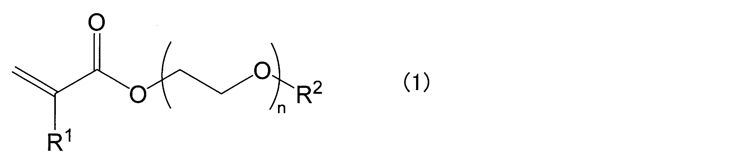
第1~第10態様のいずれか1つに係る光学積層体を備える。
第11態様に係る画像表示パネルを備える。
図1は、本実施形態に係る光学積層体の一例を模式的に示す断面図である。光学積層体10Aは、粘着シート1、静電気防止層2、及び光学フィルム3を含む。光学積層体10Aは、例えば、粘着シート1、静電気防止層2、及び光学フィルム3がこの順に積層された構造を有する。光学積層体10Aは、粘着シート1を介して、対象物(例えば、画像表示パネル)と貼り合わせることが可能である。
光学積層体10Aにおける粘着シート1側の-15℃での表面抵抗率Rは、1.0×10¹⁰Ω/□以下である。光学積層体10Aが、1.0×1010Ω/□以下の表面抵抗率Rを有する粘着シート1を備えていることによって、低温環境下であっても、画像表示装置の帯電による表示不良を抑制できる。
ポリマー(A)の例は、(メタ)アクリル系ポリマー、ウレタン系ポリマー、シリコーン系ポリマー、及びゴム系ポリマーである。ポリマー(A)は、ポリエーテル構造を有していてもよい。ポリマー(A)は、好ましくは、(メタ)アクリル系ポリマーである。換言すれば、粘着剤組成物(I)は(メタ)アクリル系ポリマーを主成分として含んでいてもよい。さらに換言すれば、粘着剤組成物(I)はアクリル系粘着剤組成物であってもよい。主成分とは、組成物において重量基準で最も含有率の大きな成分を意味する。主成分の含有率は、例えば50重量%以上であり、60重量%以上、70重量%以上、75重量%以上、さらには80重量%以上であってもよい。本明細書において、「(メタ)アクリル系ポリマー」は、(メタ)アクリレート等の(メタ)アクリル系単量体に由来する構成単位を有するポリマーを意味する。(メタ)アクリル系ポリマーにおける(メタ)アクリル系単量体に由来する構成単位の含有率は、例えば40重量%以上であり、50重量%以上、60重量%以上、70重量%以上、80重量%以上、85重量%以上、90重量%以上、さらには95重量%以上であってもよい。(メタ)アクリル系ポリマーは、(メタ)アクリル系単量体に由来する構成単位のみからなってもよい。「(メタ)アクリル」は、アクリル及びメタクリルを意味する。「(メタ)アクリレート」は、アクリレート及びメタクリレートを意味する。
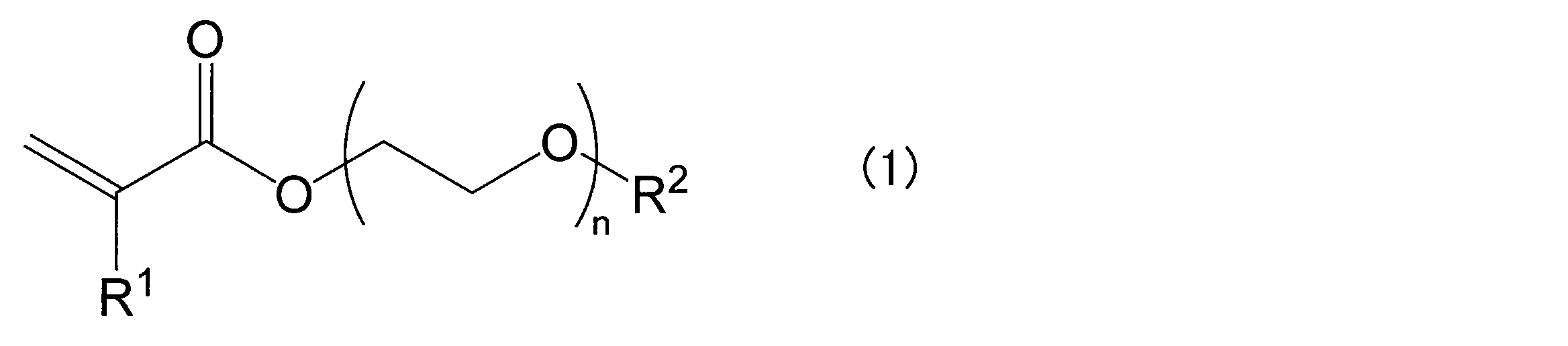
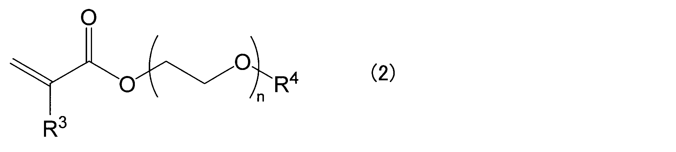
粘着剤組成物(I)は、帯電防止剤を含む。粘着剤組成物(I)は、1種又は2種以上の帯電防止剤を含んでいてもよい。帯電防止剤の例は、塩等のイオン性化合物である。イオン性化合物は、常温(25℃)で液体のイオン液体であってもよい。
(a) (CnF2n+1SO2)2N- (nは1~10の整数)
(b) CF2(CmF2mSO2)2N- (mは1~10の整数)
(c) -O3S(CF2)lSO3 - (lは1~10の整数)
(d) (CpF2p+1SO2)N-(CqF2q+1SO2) (p及びqは、互いに独立して1~10の整数)
粘着剤組成物(I)は、ラジカル捕捉剤をさらに含んでいてもよい。ラジカル捕捉剤の例は、ヒンダードフェノール系、ヒンダードアミン系、ホスファイト系、フェノール系及びチオエーテル系、並びにこれらの系統を混合したブレンド系等の各種の酸化防止剤である。
粘着剤組成物(I)は、ポリマー(A)、帯電防止剤、及びラジカル捕捉剤以外の材料をさらに含んでいてもよい。当該材料の例は、添加剤である。添加剤の例は、架橋剤、シランカップリング剤、顔料及び染料等の着色剤、紫外線吸収剤、界面活性剤、可塑剤、粘着性付与剤、表面潤滑剤、レベリング剤、リワーク向上剤、軟化剤、重合禁止剤、防錆剤、無機充填材、有機充填材、金属粉等の粉体、粒子、及び箔状物である。添加剤は、ポリマー(A)100重量部に対して合計で、例えば10重量部以下、好ましくは5重量部以下、より好ましくは3重量部以下の範囲で配合できる。
1/Tg=w1/Tg1+w2/Tg2+・・・+wm/Tgm
静電気防止層2は、導電材料を含む層である。導電材料は、ITO以外の材料であってもよく、例えば、導電性ポリマー、導電性ポリマーとドーパントとの複合体、イオン性界面活性剤、導電性微粒子、イオン性化合物等である。
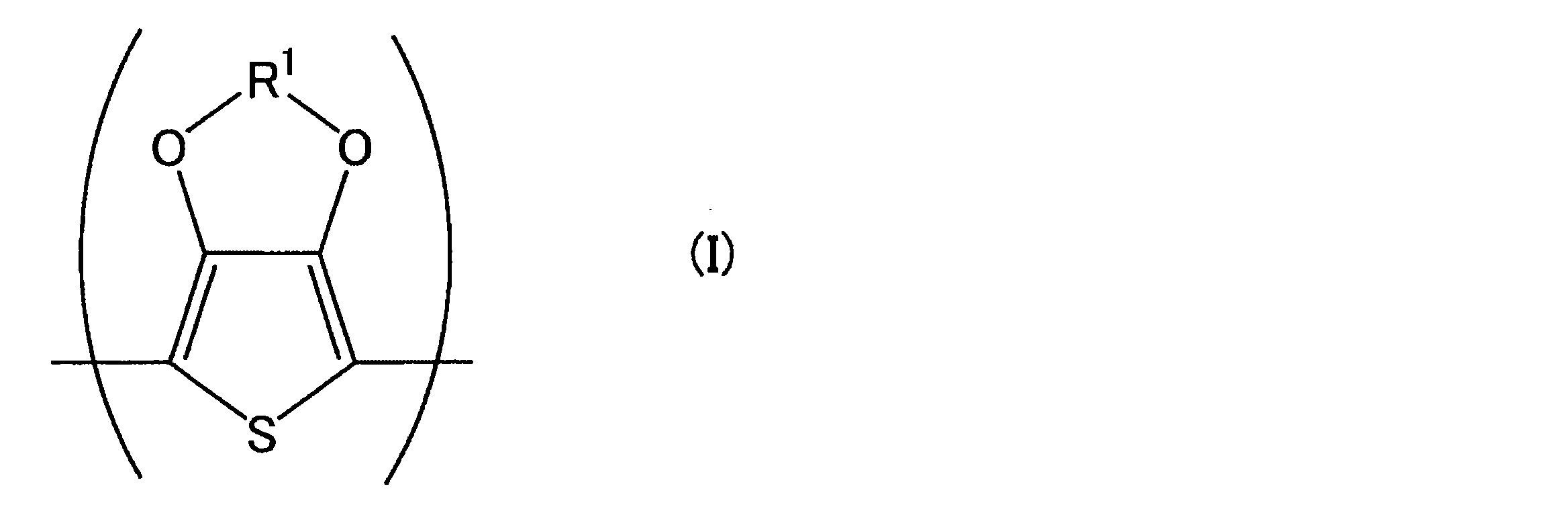
光学フィルム3は、例えば、偏光フィルム及び位相差フィルムからなる群から選ばれる少なくとも1つを含む。光学フィルム3は、偏光フィルム及び/又は位相差フィルムを含む積層フィルムであってもよい。光学フィルム3は、ガラス製のフィルムを含んでいてもよい。
光学積層体10Aは、例えば、基材及び粘着シート1からなる積層体L2を作製することと、光学フィルム3及び静電気防止層2からなる積層体L1を作製することと、積層体L2の粘着シート1を積層体L1の静電気防止層2の上に転写することと、を含む。
まず、導電材料の溶液又は分散液を調製する。溶液又は分散液の溶媒は、例えば水であり、水溶性の有機溶媒をさらに含んでいてもよい。水溶性の有機溶媒としては、例えば、メタノール、エタノール、n-プロパノール、イソプロパノール、n-ブタノール、イソブタノール、sec-ブタノール、tert-ブタノール、n-アミルアルコール、イソアミルアルコール、sec-アミルアルコール、tert-アミルアルコール、1-エチル-1-プロパノール、2-メチル-1-ブタノール、n-ヘキサノール、シクロヘキサノール等のアルコール類が挙げられる。
粘着シート1は、粘着剤組成物(I)から形成される。粘着シート1は、例えば、(メタ)アクリル系ポリマーの架橋物を含む。粘着シート1は、粘着剤組成物(I)から、以下の方法によって形成される。
図3は、本実施形態に係る画像表示パネルの一例を模式的に示す断面図である。図3に示すように、画像表示パネル11Aは、光学積層体10Aを備え、例えば画像表示セル30Aをさらに備える。詳細には、粘着シート1を介して、光学積層体10Aが画像表示セル30Aに貼り合わされている。
本実施形態の画像表示装置は、例えば、画像表示パネル11A及び照明システムを備えている。なお、画像表示パネル11Aに代えて、図4及び5の画像表示パネル11B及び11Cも使用可能である。画像表示装置において、画像表示パネル11Aは、例えば、照明システムよりも視認側に配置されている。照明システムは、例えば、バックライト又は反射板を有し、画像表示パネル11Aに光を照射する。
(メタ)アクリル系ポリマーの重量平均分子量(Mw)は、GPC(ゲル・パーミエーション・クロマトグラフィー)により測定した。(メタ)アクリル系ポリマーのMw/Mnについても、同様に測定した。
・分析装置:東ソー社製、HLC-8120GPC
・カラム:東ソー社製、G7000HXL+GMHXL+GMHXL
・カラムサイズ:各7.8mmφ×30cm 計90cm
・カラム温度:40℃
・流量:0.8mL/min
・注入量:100μL
・溶離液:テトラヒドロフラン
・検出器:示差屈折計(RI)
・標準試料:ポリスチレン
攪拌羽根、温度計、窒素ガス導入管及び冷却器を備えた4つ口フラスコに、n-ブチルアクリレート(BA)78.95重量部、フェノキシエチルアクリレート(PEA)16重量部、4-ヒドロキシブチルアクリレート(HBA)0.05重量部、及びアクリル酸(AA)5重量部を含有する単量体混合物を仕込んだ。さらに、単量体混合物100重量部に対して、重合開始剤として2,2’-アゾビスイソブチロニトリル(AIBN;キシダ化学社製)0.1重量部を酢酸エチル100重量部と共に仕込んだ。混合物を緩やかに攪拌しながら、フラスコ内について窒素ガスを導入して窒素置換した。フラスコ内の液温を55℃付近に維持して8時間重合反応を行うことによって、重量平均分子量(Mw)250万の(メタ)アクリル系ポリマーA1の溶液を調製した。FOXの式から算出した(メタ)アクリル系ポリマーA1のガラス転移温度は、-43.5℃であった。
フラスコに仕込む単量体混合物を、2-メトキシエチルアクリレート(MEA)60重量部、BA39重量部、及びHBA1重量部とした以外は、(メタ)アクリル系ポリマーA1の調製と同様にして、重量平均分子量(Mw)190万の(メタ)アクリル系ポリマーA2の溶液を調製した。FOXの式から算出した(メタ)アクリル系ポリマーA2のガラス転移温度は、-52.0℃であった。
フラスコに仕込む単量体混合物を、MEA67重量部、BA22重量部、PEA10重量部、及びHBA1重量部とした以外は、(メタ)アクリル系ポリマーA1の調製と同様にして、重量平均分子量(Mw)200万の(メタ)アクリル系ポリマーA3の溶液を調製した。FOXの式から算出した(メタ)アクリル系ポリマーA3のガラス転移温度は、-45.0℃であった。
フラスコに仕込む単量体混合物を、BA99重量部及びHBA1重量部とした以外は、(メタ)アクリル系ポリマーA1の調製と同様にして、重量平均分子量(Mw)180万の(メタ)アクリル系ポリマーA4の溶液を調製した。FOXの式から算出した(メタ)アクリル系ポリマーA4のガラス転移温度は、-55.0℃であった。
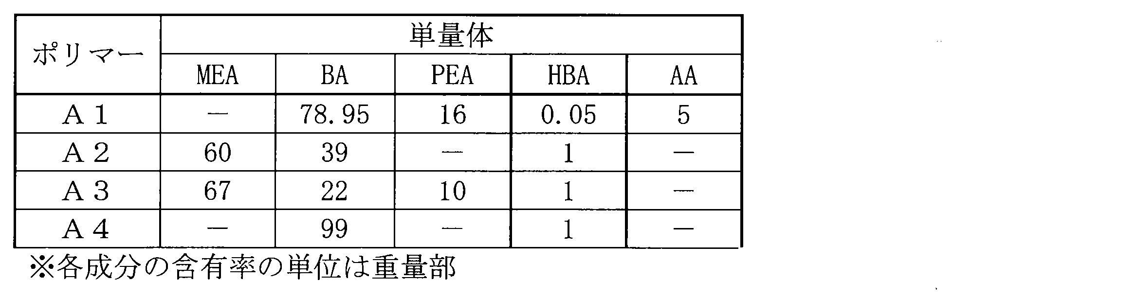
[ハードコート層付きTACフィルム]
まず、ウレタンアクリレートを主成分として含む紫外線硬化型樹脂モノマー又はオリゴマーが酢酸ブチルに溶解している樹脂溶液(DIC社製,商品名:ユニディック17-806、固形分濃度:80%)を準備した。この樹脂溶液の固形分100重量部に対して、光重合開始剤(BASF社製、商品名:IRGACURE907)5重量部及びレベリング剤(DIC社製、商品名:GRANDIC PC4100)0.1重量部を樹脂溶液に添加した。次に、樹脂溶液中の固形分濃度が36%に調節されるように、樹脂溶液にシクロペンタノンとプロピレングリコールモノメチルエーテルを45:55の重量比率で加えた。これにより、ハードコート層形成材料を作製した。得られた形成材料を厚み40μmのトリアセチルセルロースを含む透明保護フィルム(コニカミノルタ社製のTACフィルム、商品名「KC4UY」)の上に塗布して塗膜を形成した。このとき、形成材料を硬化することによって得られるハードコート層の厚さが7μmに調節されるように塗膜の厚さを調節した。次に、塗膜を90℃で1分間乾燥し、さらに高圧水銀ランプにて積算光量300mJ/cm2の紫外線を塗膜に照射した。これにより、塗膜が硬化し、ハードコート層(HC)付きTACフィルムが得られた。
まず、速度比が互いに異なる複数のロールの間において、厚さ80μmのポリビニルアルコールフィルムを濃度0.3%のヨウ素溶液(温度30℃)中で1分間染色しながら、延伸倍率が3倍になるように延伸した。次に、得られた延伸フィルムをホウ酸の濃度が4%であり、ヨウ化カリウムの濃度が10%である水溶液(温度60℃)中に0.5分間浸漬しながら、総延伸倍率が6倍になるように延伸した。次に、延伸フィルムを濃度1.5%のヨウ化カリウムを含む水溶液(温度30℃)中に10秒間浸漬することによって洗浄した。次に、延伸フィルムを50℃で4分間乾燥させることによって、厚さ30μmの偏光子を得た。得られた偏光子の一方の主面には、ポリビニルアルコール系接着剤を介して、ラクトン環構造を有する変性アクリル系ポリマーからなる透明保護フィルム(厚さ30μm)を接合させた。偏光子の他方の主面には、ポリビニルアルコール系接着剤を介して、上述したハードコート層付きTACフィルム(厚さ47μm)を接合させた。このとき、偏光子の他方の主面を透明保護フィルムと接合させた。偏光子と透明保護フィルムとの接合は、ロール貼合機を用いて行った。偏光子と透明保護フィルムとを接合させた後に、オーブンを用いて、得られた積層体を70℃で5分間加熱乾燥させることによってハードコート層及び偏光フィルムからなる偏光板を得た。
まず、PEDOT/PSSを含む溶液(ナガセケムテックス社製、品番:N006-45-2A、N006-45-2B)50部及び水50部を混合することによって、固形分濃度が0.5重量%である塗布液を調製した。次に、塗布液を偏光板の偏光フィルム側の表面に塗布した。得られた塗布膜を80℃で2分間乾燥させることによって静電気防止層を作製した。これにより、偏光板及び静電気防止層からなる積層体L1を得た。静電気防止層の厚さは、60nmであった。
(メタ)アクリル系ポリマーA1の溶液の固形分100重量部に対して、0.3重量部の架橋剤(東ソー社製、製品名;コロネート2770)、帯電防止剤として20重量部の1-エチル-3-メチルイミダゾリウムビス(フルオロスルホニル)イミド(EMI-FSI)(第一工業製薬社製、製品名;エレクセルAS110)、0.5重量部の酸化防止剤(BASF社製、製品名;Irganox1010)、及び0.4重量部のシランカップリング剤(カネカ社製、製品名;サイリルSAT010)をさらに配合することによって、実施例1の(メタ)アクリル系粘着剤組成物の溶液を調製した。
次に、上記で得られた積層体L2の粘着シートを積層体L1の静電気防止層の上に転写することによって、偏光板、静電気防止層、粘着シート、及びはく離ライナーがこの順に積層された積層体L3を作製した。積層体L3からはく離ライナーを剥離することによって、実施例1に係る光学積層体を得た。
粘着シートの作製において、(メタ)アクリル系ポリマーA2の溶液を使用したことと、(メタ)アクリル系ポリマーA2の溶液の固形分100重量部に対して、帯電防止剤としてEMI-FSIを6重量部使用したことと、を除き、実施例1と同じ方法によって実施例2に係る光学積層体を得た。
静電気防止層の厚さが130nmとなるように、PEDOT/PSSの塗布液を偏光フィルムに塗布したことを除き、実施例2と同じ方法によって実施例3に係る光学積層体を得た。
以下の方法によって、粘着シート及び静電気防止層を作製したことを除き、実施例1と同じ方法で実施例4に係る光学積層体を得た。まず、粘着シートの作製において、(メタ)アクリル系ポリマーA3の溶液を使用した。(メタ)アクリル系ポリマーA3の溶液の固形分100重量部に対して、帯電防止剤としてEMI-FSIを8重量部使用した。静電気防止層の厚さが30nmとなるように、PEDOT/PSSの塗布液を偏光フィルムに塗布した。
静電気防止層の厚さが60nmとなるように、PEDOT/PSSの塗布液を偏光フィルムに塗布したことを除き、実施例4と同じ方法によって実施例5に係る光学積層体を得た。
静電気防止層の厚さが130nmとなるように、PEDOT/PSSの塗布液を偏光フィルムに塗布したことを除き、実施例4と同じ方法によって実施例6に係る光学積層体を得た。
以下の方法によって、偏光板及び静電気防止層からなる積層体L1を作製したことを除き、実施例4と同じ方法によって実施例7に係る光学積層体を得た。まず、CNT及びウレタン系バインダーを含む溶液(ナガセケムテックス社製、製品名:C-100A)14重量部及び水86重量部を混合することによって、固形分濃度が0.5重量%である塗布液を調製した。次に、塗布液を上述の偏光板の偏光フィルム側の主面に塗布した。得られた塗布膜を90℃で1分間乾燥させることによって静電気防止層を作製した。これにより、偏光板及び静電気防止層からなる積層体L1を得た。静電気防止層の厚さは、55nmであった。
CNT及びウレタン系バインダーを含む溶液(ナガセケムテックス社製、製品名:C-100A)15.1重量部、オキサゾリン基を含有するバインダー(日本触媒社製、製品名:エポクロス(登録商標)WS-700)0.7重量部、及び水84重量部を混合することによって、固形分濃度が0.5重量%である塗布液を上述の偏光板の偏光フィルム側の主面に塗布したことを除き、実施例7と同じ方法によって実施例8に係る光学積層体を得た。
粘着シートの作製において、(メタ)アクリル系ポリマーA2の溶液の固形分100重量部に対して、帯電防止剤としてEMI-FSIを15重量部使用したことと、静電気防止層の厚さが30nmとなるように、PEDOT/PSSの塗布液を偏光フィルムに塗布したことと、を除き、実施例2と同じ方法によって実施例10に係る光学積層体を得た。
以下の方法によって粘着シートを作製したことと、静電気防止層を作製しなかったことと、を除き、実施例1と同じ方法で比較例1に係る光学積層体を得た。粘着シートの作製において、(メタ)アクリル系ポリマーA4の溶液を使用した。(メタ)アクリル系ポリマーA4の溶液の固形分100重量部に対して、帯電防止剤としてEMI-FSIを10重量部使用した。
各実施例及び比較例において、はく離ライナーの表面に粘着シートが形成された積層体L2を用いて、粘着シートの25℃での表面抵抗率を測定した。積層体L2における粘着シートの表面抵抗率の測定は、抵抗率計(三菱ケミカルアナリテック社製のハイレスタ MCP-HT800)を用いて、印加電圧250V、印加時間10秒の条件で実施した。
各実施例及び比較例において、偏光板及び静電気防止層からなる積層体L1を用いて、静電気防止層の表面抵抗率を測定した。静電気防止層の25℃での表面抵抗率の測定は、上記した抵抗率計を用いて、JIS K6911:1995に規定された方法に準拠して、印加電圧10V、印加時間10秒の条件で実施した。
各実施例及び比較例に係る光学積層体を用いて、粘着シート側の表面抵抗率を測定した。光学積層体における粘着シート側の室温(25℃)での表面抵抗率R1の測定は、上記した抵抗率計を用いて、印加電圧250V、印加時間10秒の条件で実施した。
光学積層体の耐久性は、以下の方法により評価した。作製した光学積層体を、その粘着シートを介してガラス板(コーニング製、イーグルXG)の表面に固定してガラス板付き光学積層体を得た。固定は、24℃及び50%RHの雰囲気で実施した。次に、ガラス板付き光学積層体を50℃及び5気圧(絶対圧)のオートクレーブにて15分処理した後、24℃に冷えるまで放置して、ガラス板への光学積層体の接合を安定させた。次に、ガラス板付き光学積層体を105℃の加熱雰囲気に500時間静置した。静置後、24℃及び50%RHの雰囲気に戻し、ガラス板からの偏光板の剥がれ、ガラス板と偏光板との間に発泡が生じていないか、を目視により確認して、以下のように、耐久性を評価した。
(評価基準)
A:発泡や剥がれ等の外観上の変化がみられない。
B:端部において、単独の剥がれ又は発泡がわずかにみられるが、実用上、問題ない範囲にある。
C:端部において、連続した剥がれ又は発泡がわずかにみられるが、実用上、問題ない範囲にある。
D:端部に著しい剥がれ又は発泡がみられ、実用上、問題がある。
光学積層体の白抜けは、耐候性試験の前後において、以下の方法により評価した。作製した光学積層体の光学フィルム側に、OCA(日東電工社製、LUCIACS CS9821;アクリル酸モノマーフリー粘着剤、厚さ200μm)を介して、前面透明部材を模したガラス板を貼り合わせて、画像表示装置を模した評価用の積層体を作製した。次に、評価用の積層体を、その粘着シートを介して、インセル型液晶セルの視認側に貼り合わせることによって、積層体付きインセル型液晶セルを作製した。次に、積層体付きインセル型液晶セルの視認側と反対側に、クロスニコルの関係になるように偏光板を貼り合わせることによって液晶表示パネルを作製した。この液晶表示パネルを、-15℃に設定したコールドプレートで冷却後、すぐにバックライト装置上にセットし、視認側の偏光板面をニトリル手袋で数回擦ることによって静電気を発生させた。静電気により生じた、白抜けした部分が消失するまでの時間を測定して、下記の基準により評価した。耐候性試験は、紫外線フェード試験機(スガ試験機社製、U48HB)を用いて、上述の方法によって実施した。なお、実用上問題となる評価結果は、「D」である。
(評価基準)
A:白抜けが発生しない。
B:数回擦ると白抜けが発生するが、1秒以内に消失する。
C:数回擦ると白抜けが発生するが、1秒を超え、5秒未満に消失する。
D:一回擦るだけで白抜けが発生し、消失までに5秒以上かかる。
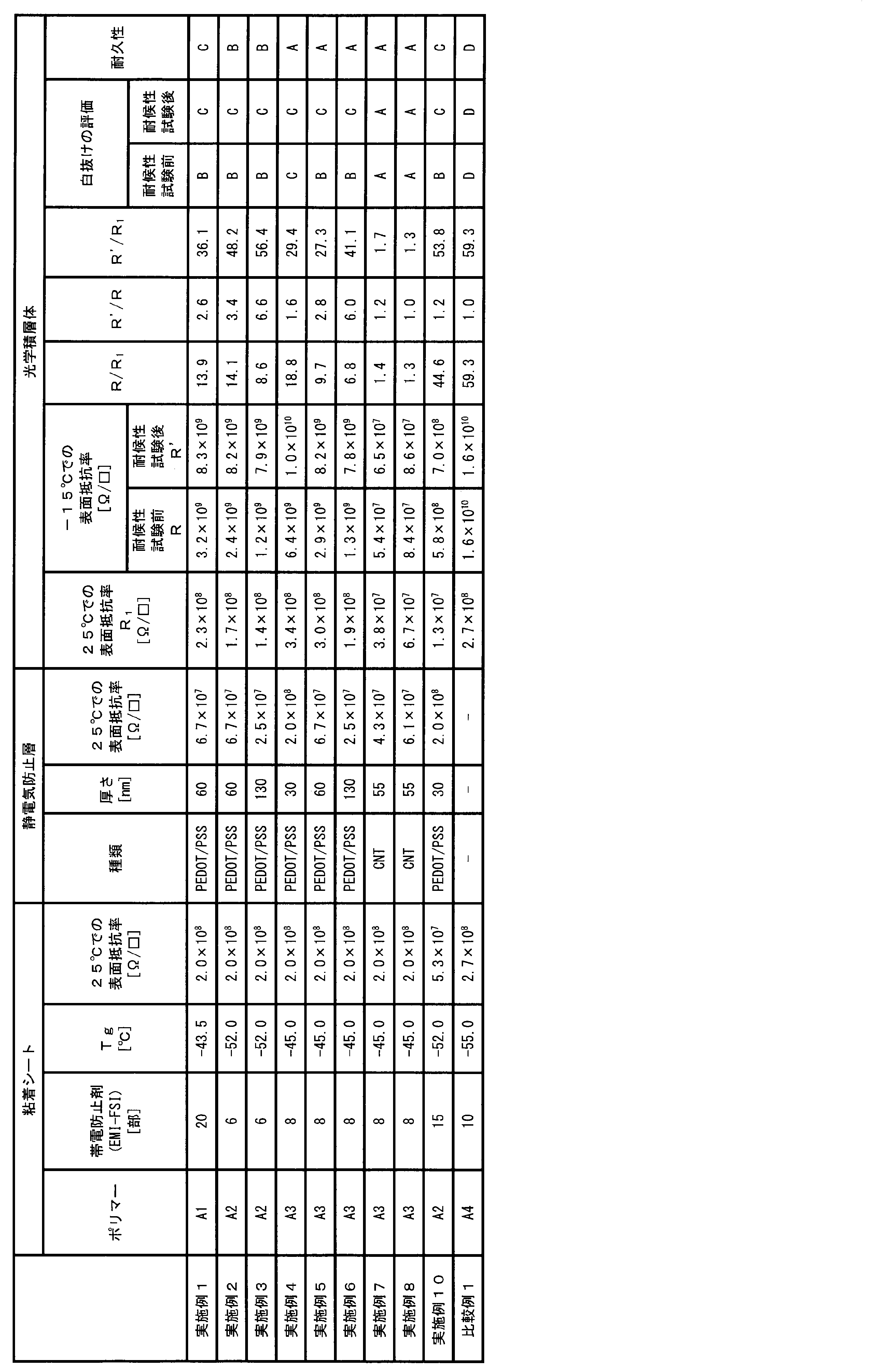
Claims (12)
- 粘着シートと、静電気防止層と、光学フィルムと、を備えた光学積層体であって、
前記粘着シートは、ポリマー(A)と帯電防止剤とを含む粘着剤組成物から形成され、
前記光学積層体における前記粘着シート側の-15℃での表面抵抗率が1.0×10¹⁰Ω/□以下である、光学積層体。 - 前記静電気防止層の25℃での表面抵抗率が3.0×10⁸Ω/□以下である、請求項1に記載の光学積層体。
- 前記静電気防止層の25℃での表面抵抗率が1.0×10⁷Ω/□以上1.0×108Ω/□未満である、請求項2に記載の光学積層体。
- 前記ポリマー(A)は、(メタ)アクリル系ポリマーである、請求項1に記載の光学積層体。
- 前記ポリマー(A)は、ポリエーテル構造を有する、請求項1に記載の光学積層体。
- 前記ポリマー(A)は、以下の式(1)に示す単量体に由来する構成単位を有する、請求項1に記載の光学積層体。
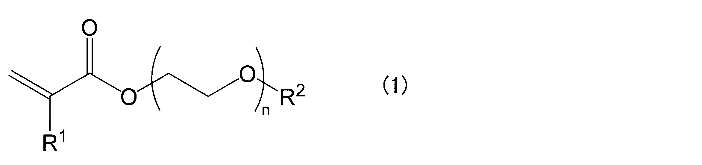
- 前記ポリマー(A)は、芳香環含有単量体に由来する構成単位を有する、請求項5に記載の光学積層体。
- 前記粘着剤組成物において、前記ポリマー(A)100重量部に対する前記帯電防止剤の配合量が10重量部未満である、請求項1に記載の光学積層体。
- FOXの式から算出した前記ポリマー(A)のガラス転移温度が-40℃以下である、請求項1に記載の光学積層体。
- 前記ガラス転移温度が-45℃以下である、請求項9に記載の光学積層体。
- 請求項1~10のいずれか1項に記載の光学積層体を備える、画像表示パネル。
- 請求項11に記載の画像表示パネルを備える、画像表示装置。
Priority Applications (3)
| Application Number | Priority Date | Filing Date | Title |
|---|---|---|---|
| KR1020257020881A KR20250153756A (ko) | 2023-03-16 | 2024-03-13 | 광학 적층체, 화상 표시 패널, 및 화상 표시 장치 |
| KR1020257006818A KR102826219B1 (ko) | 2023-03-16 | 2024-03-13 | 광학 적층체, 화상 표시 패널, 및 화상 표시 장치 |
| CN202480004187.4A CN119895295A (zh) | 2023-03-16 | 2024-03-13 | 光学层叠体、图像显示面板及图像显示装置 |
Applications Claiming Priority (2)
| Application Number | Priority Date | Filing Date | Title |
|---|---|---|---|
| JP2023-041857 | 2023-03-16 | ||
| JP2023041857 | 2023-03-16 |
Publications (1)
| Publication Number | Publication Date |
|---|---|
| WO2024190847A1 true WO2024190847A1 (ja) | 2024-09-19 |
Family
ID=92755272
Family Applications (1)
| Application Number | Title | Priority Date | Filing Date |
|---|---|---|---|
| PCT/JP2024/009899 Ceased WO2024190847A1 (ja) | 2023-03-16 | 2024-03-13 | 光学積層体、画像表示パネル、及び画像表示装置 |
Country Status (5)
| Country | Link |
|---|---|
| JP (2) | JP2024133005A (ja) |
| KR (2) | KR102826219B1 (ja) |
| CN (1) | CN119895295A (ja) |
| TW (2) | TWI891283B (ja) |
| WO (1) | WO2024190847A1 (ja) |
Families Citing this family (1)
| Publication number | Priority date | Publication date | Assignee | Title |
|---|---|---|---|---|
| JP7839846B1 (ja) * | 2024-11-06 | 2026-04-02 | 日東電工株式会社 | 静電気防止層の製造方法及び光学積層体の製造方法 |
Citations (4)
| Publication number | Priority date | Publication date | Assignee | Title |
|---|---|---|---|---|
| JP2021096308A (ja) * | 2019-12-13 | 2021-06-24 | 日東電工株式会社 | 粘着剤層付き光学フィルム及び液晶パネル |
| JP2022074622A (ja) * | 2020-11-05 | 2022-05-18 | 日東電工株式会社 | 偏光板およびそれを用いた画像表示装置 |
| KR20220070999A (ko) * | 2020-11-23 | 2022-05-31 | 에스케이씨하이테크앤마케팅(주) | 점착제 조성물 및 이를 이용한 보호필름 |
| JP2022129959A (ja) * | 2021-02-25 | 2022-09-06 | 日東電工株式会社 | 偏光板およびそれを用いた画像表示装置 |
Family Cites Families (11)
| Publication number | Priority date | Publication date | Assignee | Title |
|---|---|---|---|---|
| CN101089112A (zh) * | 2006-06-16 | 2007-12-19 | 住友化学株式会社 | 抗静电剂组合物 |
| CN102012532B (zh) * | 2009-09-03 | 2015-05-20 | 株式会社巴川制纸所 | 光学层叠体、偏振片及使用其的显示装置 |
| IN2014DN06950A (ja) | 2012-02-28 | 2015-04-10 | Heraeus Precious Metals Gmbh | |
| CN103451757A (zh) * | 2013-06-17 | 2013-12-18 | 江南大学 | 一种具有抗静电、耐酸碱、隔热阻燃特性的纤维 |
| CN104419052A (zh) * | 2013-09-05 | 2015-03-18 | 青岛欣展塑胶有限公司 | 核壳粒子增韧聚乙烯抗静电母粒及其制备方法 |
| JP5812311B1 (ja) | 2014-08-08 | 2015-11-11 | ナガセケムテックス株式会社 | 透明導電体、液晶表示装置及び透明導電体の製造方法 |
| KR102071913B1 (ko) * | 2016-05-31 | 2020-01-31 | 주식회사 엘지화학 | 광학 필름 |
| WO2020262395A1 (ja) * | 2019-06-28 | 2020-12-30 | 日東電工株式会社 | 粘着剤層付き偏光フィルム及び液晶パネル |
| CN118918775A (zh) * | 2020-03-09 | 2024-11-08 | 大日本印刷株式会社 | 柔性显示装置用层积体、显示装置用层积体和柔性显示装置 |
| CN116097137A (zh) * | 2020-11-05 | 2023-05-09 | 日东电工株式会社 | 偏振片及使用了该偏振片的图像显示装置 |
| CN117157559A (zh) * | 2021-04-02 | 2023-12-01 | 日产化学株式会社 | 抗静电硬涂层及固化性组合物 |
-
2024
- 2024-03-13 CN CN202480004187.4A patent/CN119895295A/zh active Pending
- 2024-03-13 WO PCT/JP2024/009899 patent/WO2024190847A1/ja not_active Ceased
- 2024-03-13 JP JP2024039500A patent/JP2024133005A/ja active Pending
- 2024-03-13 KR KR1020257006818A patent/KR102826219B1/ko active Active
- 2024-03-13 KR KR1020257020881A patent/KR20250153756A/ko active Pending
- 2024-03-15 TW TW113109579A patent/TWI891283B/zh active
- 2024-03-15 TW TW114125446A patent/TW202541993A/zh unknown
- 2024-11-27 JP JP2024206314A patent/JP7637308B1/ja active Active
Patent Citations (4)
| Publication number | Priority date | Publication date | Assignee | Title |
|---|---|---|---|---|
| JP2021096308A (ja) * | 2019-12-13 | 2021-06-24 | 日東電工株式会社 | 粘着剤層付き光学フィルム及び液晶パネル |
| JP2022074622A (ja) * | 2020-11-05 | 2022-05-18 | 日東電工株式会社 | 偏光板およびそれを用いた画像表示装置 |
| KR20220070999A (ko) * | 2020-11-23 | 2022-05-31 | 에스케이씨하이테크앤마케팅(주) | 점착제 조성물 및 이를 이용한 보호필름 |
| JP2022129959A (ja) * | 2021-02-25 | 2022-09-06 | 日東電工株式会社 | 偏光板およびそれを用いた画像表示装置 |
Also Published As
| Publication number | Publication date |
|---|---|
| TW202541993A (zh) | 2025-11-01 |
| JP2024133005A (ja) | 2024-10-01 |
| TWI891283B (zh) | 2025-07-21 |
| TW202442442A (zh) | 2024-11-01 |
| KR102826219B1 (ko) | 2025-06-27 |
| KR20250040739A (ko) | 2025-03-24 |
| JP7637308B1 (ja) | 2025-02-27 |
| KR20250153756A (ko) | 2025-10-27 |
| CN119895295A (zh) | 2025-04-25 |
| JP2025037962A (ja) | 2025-03-18 |
Similar Documents
| Publication | Publication Date | Title |
|---|---|---|
| JP7637308B1 (ja) | 光学積層体、画像表示パネル、及び画像表示装置 | |
| CN114746776A (zh) | 带粘合剂层的光学膜及液晶面板 | |
| JP7369887B2 (ja) | 粘着剤組成物、粘着シート、光学積層体、画像表示パネル及び画像表示装置 | |
| JP2023073210A (ja) | 粘着剤組成物、粘着シート、光学積層体、画像表示パネル及び画像表示装置 | |
| JP7369886B2 (ja) | 粘着剤組成物、粘着シート、光学積層体、画像表示パネル及び画像表示装置 | |
| KR20250008726A (ko) | 광학 적층체, 화상 표시 패널 및 화상 표시 장치 | |
| TWI916622B (zh) | 黏著劑組成物、黏著片、光學積層體、影像顯示面板及影像顯示裝置 | |
| KR20240104119A (ko) | 터치 센싱 기능을 내장하는 화상 표시 패널 및 화상 표시 장치 | |
| WO2024190407A1 (ja) | 光学積層体、画像表示パネル、及び画像表示装置 | |
| WO2025089363A1 (ja) | 光学積層体、画像表示パネル及び画像表示装置 | |
| WO2025089364A1 (ja) | 光学積層体、画像表示パネル及び画像表示装置 | |
| WO2025249336A1 (ja) | 光学積層体、画像表示パネル及び画像表示装置 | |
| JP7839846B1 (ja) | 静電気防止層の製造方法及び光学積層体の製造方法 | |
| JP2025181261A (ja) | 光学積層体、画像表示パネル及び画像表示装置 | |
| KR20240101606A (ko) | 광학 적층체, 화상 표시 패널 및 화상 표시 장치 | |
| CN118234826A (zh) | 粘合剂组合物、粘合片、光学层叠体、图像显示面板及图像显示装置 |
Legal Events
| Date | Code | Title | Description |
|---|---|---|---|
| 121 | Ep: the epo has been informed by wipo that ep was designated in this application |
Ref document number: 24770950 Country of ref document: EP Kind code of ref document: A1 |
|
| ENP | Entry into the national phase |
Ref document number: 20257006818 Country of ref document: KR Kind code of ref document: A |
|
| WWP | Wipo information: published in national office |
Ref document number: 1020257006818 Country of ref document: KR |
|
| WWE | Wipo information: entry into national phase |
Ref document number: 202480004187.4 Country of ref document: CN |
|
| WWP | Wipo information: published in national office |
Ref document number: 202480004187.4 Country of ref document: CN |
|
| NENP | Non-entry into the national phase |
Ref country code: DE |
|
| WWP | Wipo information: published in national office |
Ref document number: 1020257020881 Country of ref document: KR |
|
| 122 | Ep: pct application non-entry in european phase |
Ref document number: 24770950 Country of ref document: EP Kind code of ref document: A1 |