WO2024190423A1 - 電子装置 - Google Patents
電子装置 Download PDFInfo
- Publication number
- WO2024190423A1 WO2024190423A1 PCT/JP2024/007386 JP2024007386W WO2024190423A1 WO 2024190423 A1 WO2024190423 A1 WO 2024190423A1 JP 2024007386 W JP2024007386 W JP 2024007386W WO 2024190423 A1 WO2024190423 A1 WO 2024190423A1
- Authority
- WO
- WIPO (PCT)
- Prior art keywords
- conductor
- electronic device
- electronic component
- thickness direction
- columnar conductor
- Prior art date
- Legal status (The legal status is an assumption and is not a legal conclusion. Google has not performed a legal analysis and makes no representation as to the accuracy of the status listed.)
- Ceased
Links
Images









Classifications
-
- H—ELECTRICITY
- H05—ELECTRIC TECHNIQUES NOT OTHERWISE PROVIDED FOR
- H05K—PRINTED CIRCUITS; CASINGS OR CONSTRUCTIONAL DETAILS OF ELECTRIC APPARATUS; MANUFACTURE OF ASSEMBLAGES OF ELECTRICAL COMPONENTS
- H05K1/00—Printed circuits
- H05K1/18—Printed circuits structurally associated with non-printed electric components
-
- H—ELECTRICITY
- H05—ELECTRIC TECHNIQUES NOT OTHERWISE PROVIDED FOR
- H05K—PRINTED CIRCUITS; CASINGS OR CONSTRUCTIONAL DETAILS OF ELECTRIC APPARATUS; MANUFACTURE OF ASSEMBLAGES OF ELECTRICAL COMPONENTS
- H05K9/00—Screening of apparatus or components against electric or magnetic fields
-
- H—ELECTRICITY
- H10—SEMICONDUCTOR DEVICES; ELECTRIC SOLID-STATE DEVICES NOT OTHERWISE PROVIDED FOR
- H10W—GENERIC PACKAGES, INTERCONNECTIONS, CONNECTORS OR OTHER CONSTRUCTIONAL DETAILS OF DEVICES COVERED BY CLASS H10
- H10W42/00—Arrangements for protection of devices
- H10W42/20—Arrangements for protection of devices protecting against electromagnetic or particle radiation, e.g. light, X-rays, gamma-rays or electrons
-
- H—ELECTRICITY
- H10—SEMICONDUCTOR DEVICES; ELECTRIC SOLID-STATE DEVICES NOT OTHERWISE PROVIDED FOR
- H10W—GENERIC PACKAGES, INTERCONNECTIONS, CONNECTORS OR OTHER CONSTRUCTIONAL DETAILS OF DEVICES COVERED BY CLASS H10
- H10W70/00—Package substrates; Interposers; Redistribution layers [RDL]
- H10W70/60—Insulating or insulated package substrates; Interposers; Redistribution layers
-
- H—ELECTRICITY
- H10—SEMICONDUCTOR DEVICES; ELECTRIC SOLID-STATE DEVICES NOT OTHERWISE PROVIDED FOR
- H10W—GENERIC PACKAGES, INTERCONNECTIONS, CONNECTORS OR OTHER CONSTRUCTIONAL DETAILS OF DEVICES COVERED BY CLASS H10
- H10W70/00—Package substrates; Interposers; Redistribution layers [RDL]
- H10W70/60—Insulating or insulated package substrates; Interposers; Redistribution layers
- H10W70/611—Insulating or insulated package substrates; Interposers; Redistribution layers for connecting multiple chips together
-
- H—ELECTRICITY
- H10—SEMICONDUCTOR DEVICES; ELECTRIC SOLID-STATE DEVICES NOT OTHERWISE PROVIDED FOR
- H10W—GENERIC PACKAGES, INTERCONNECTIONS, CONNECTORS OR OTHER CONSTRUCTIONAL DETAILS OF DEVICES COVERED BY CLASS H10
- H10W70/00—Package substrates; Interposers; Redistribution layers [RDL]
- H10W70/60—Insulating or insulated package substrates; Interposers; Redistribution layers
- H10W70/62—Insulating or insulated package substrates; Interposers; Redistribution layers characterised by their interconnections
- H10W70/63—Vias, e.g. via plugs
- H10W70/635—Through-vias
-
- H—ELECTRICITY
- H10—SEMICONDUCTOR DEVICES; ELECTRIC SOLID-STATE DEVICES NOT OTHERWISE PROVIDED FOR
- H10W—GENERIC PACKAGES, INTERCONNECTIONS, CONNECTORS OR OTHER CONSTRUCTIONAL DETAILS OF DEVICES COVERED BY CLASS H10
- H10W70/00—Package substrates; Interposers; Redistribution layers [RDL]
- H10W70/60—Insulating or insulated package substrates; Interposers; Redistribution layers
- H10W70/67—Insulating or insulated package substrates; Interposers; Redistribution layers characterised by their insulating layers or insulating parts
- H10W70/69—Insulating materials thereof
-
- H—ELECTRICITY
- H10—SEMICONDUCTOR DEVICES; ELECTRIC SOLID-STATE DEVICES NOT OTHERWISE PROVIDED FOR
- H10W—GENERIC PACKAGES, INTERCONNECTIONS, CONNECTORS OR OTHER CONSTRUCTIONAL DETAILS OF DEVICES COVERED BY CLASS H10
- H10W99/00—Subject matter not provided for in other groups of this subclass
-
- H—ELECTRICITY
- H10—SEMICONDUCTOR DEVICES; ELECTRIC SOLID-STATE DEVICES NOT OTHERWISE PROVIDED FOR
- H10W—GENERIC PACKAGES, INTERCONNECTIONS, CONNECTORS OR OTHER CONSTRUCTIONAL DETAILS OF DEVICES COVERED BY CLASS H10
- H10W90/00—Package configurations
-
- H—ELECTRICITY
- H10—SEMICONDUCTOR DEVICES; ELECTRIC SOLID-STATE DEVICES NOT OTHERWISE PROVIDED FOR
- H10W—GENERIC PACKAGES, INTERCONNECTIONS, CONNECTORS OR OTHER CONSTRUCTIONAL DETAILS OF DEVICES COVERED BY CLASS H10
- H10W90/00—Package configurations
- H10W90/701—Package configurations characterised by the relative positions of pads or connectors relative to package parts
- H10W90/721—Package configurations characterised by the relative positions of pads or connectors relative to package parts of bump connectors
- H10W90/724—Package configurations characterised by the relative positions of pads or connectors relative to package parts of bump connectors between a chip and a stacked insulating package substrate, interposer or RDL
Definitions
- This disclosure relates to electronic devices.
- Patent Document 1 discloses an example of a conventional electronic device.
- the electronic device (semiconductor device) described in Patent Document 1 includes a semiconductor element, multiple electronic components, an insulating layer, and a sealing resin.
- the semiconductor element is an LSI.
- Each of the multiple electronic components is either a passive element such as a resistor, a capacitor, or an inductor, or a diode.
- the insulating layer supports the semiconductor element and multiple electronic components.
- the sealing resin is formed on the insulating layer. The sealing resin covers the semiconductor element and multiple electronic components.
- One of the objectives of this disclosure is to provide an electronic device that is an improvement over conventional devices.
- one of the objectives of this disclosure is to provide an electronic device that can improve operational reliability.
- An electronic device provided by one aspect of the present disclosure includes a first electronic component, a support member having a support surface that supports the first electronic component, a columnar conductor arranged in a direction in which the support surface faces the support member, and a sealing resin formed on the support surface and covering the first electronic component.
- the columnar conductor has a conductor top surface that faces in the same direction as the support surface in the thickness direction of the support member. The conductor top surface is covered with the sealing resin.
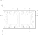
- FIG. 1 is a plan view showing an electronic device according to a first embodiment.
- FIG. 2 is a plan view of FIG. 1, in which the sealing resin is shown by imaginary lines.
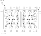
- FIG. 3 is a plan view of FIG. 2 with the sealing resin and the columnar conductors omitted, and the first electronic component and the second electronic component shown by imaginary lines.
- FIG. 4 is a front view of the electronic device according to the first embodiment.
- FIG. 5 is a bottom view of the electronic device according to the first embodiment.
- FIG. 6 is a left side view showing the electronic device according to the first embodiment.
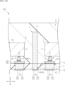
- FIG. 7 is a cross-sectional view taken along line VII-VII in FIG.
- FIG. 8 is a partially enlarged view of a part of FIG. FIG.
- FIG. 9 is a cross-sectional view showing a step of the method for manufacturing an electronic device according to the first embodiment, and corresponds to the cross section of FIG.
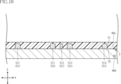
- FIG. 10 is a cross-sectional view showing a step of the method for manufacturing an electronic device according to the first embodiment, and corresponds to the cross section of FIG.
- FIG. 11 is a cross-sectional view showing a step of the method for manufacturing an electronic device according to the first embodiment, and corresponds to the cross section of FIG.
- FIG. 12 is a cross-sectional view showing a step of the method for manufacturing an electronic device according to the first embodiment, and corresponds to the cross section of FIG. FIG.
- FIG. 13 is a cross-sectional view showing a step of the method for manufacturing an electronic device according to the first embodiment, and corresponds to the cross section of FIG.
- FIG. 14 is a cross-sectional view showing a step of the method for manufacturing an electronic device according to the first embodiment, and corresponds to the cross section of FIG.
- FIG. 15 is a cross-sectional view showing a step of the method for manufacturing an electronic device according to the first embodiment, and corresponds to the cross section of FIG.
- FIG. 16 is a cross-sectional view showing a step of the method for manufacturing an electronic device according to the first embodiment, and corresponds to the cross section of FIG. FIG.
- FIG. 17 is a cross-sectional view showing a step of the method for manufacturing an electronic device according to the first embodiment, and corresponds to the cross section of FIG.
- FIG. 18 is a cross-sectional view showing a step of the method for manufacturing an electronic device according to the first embodiment, and corresponds to the cross section of FIG.
- FIG. 19 is an enlarged cross-sectional view of a main part showing an electronic device according to a first modified example of the first embodiment, and corresponds to FIG.
- FIG. 20 is an enlarged cross-sectional view of a main part showing an electronic device according to a second modified example of the first embodiment, and corresponds to FIG.
- FIG. 21 is a bottom view showing an electronic device according to a third modified example of the first embodiment.
- FIG. 22 is a cross-sectional view taken along line XXII-XXII in FIG.
- FIG. 23 is a plan view showing an electronic device according to the second embodiment, in which the sealing resin is shown by imaginary lines.
- FIG. 24 is a plan view showing an electronic device according to a modified example of the second embodiment, in which the sealing resin is indicated by imaginary lines.
- FIG. 25 is a plan view showing an electronic device according to the third embodiment, in which the sealing resin is shown by imaginary lines.
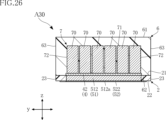
- FIG. 26 is a cross-sectional view taken along line XXVI-XXVI in FIG.
- FIG. 27 is a plan view showing an electronic device according to a modified example of the third embodiment, in which the sealing resin is indicated by imaginary lines.
- FIG. 28 is a plan view showing an electronic device according to another embodiment, in which a sealing resin is shown by imaginary lines.
- FIG. 29 is a cross-sectional view taken along line XXIX-XXIX in FIG.
- an object A is formed on an object B
- an object A is formed on (an object B)
- an object A is formed directly on an object B
- an object A is formed on an object B with another object interposed between the object A and the object B” unless otherwise specified.
- an object A is disposed on an object B” and “an object A is disposed on (an object B)” include “an object A is disposed directly on an object B” and “an object A is disposed on (an object B) with another object interposed between the object A and the object B” unless otherwise specified.
- an object A is located on (an object B) includes “an object A is in contact with an object B and is located on (an object B)” and “an object A is located on (an object B) with another object interposed between the object A and the object B".
- an object A overlaps an object B includes “an object A overlaps the entire object B” and “an object A overlaps a part of an object B", unless otherwise specified.
- an object A (its material) contains a certain material C includes “an object A (its material) is made of a certain material C” and “an object A (its material) is mainly made of a certain material C”.
- a certain surface A faces a certain direction B (to one side or the other)
- FIGS 1 to 8 show an electronic device A10 according to a first embodiment.
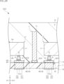
- the electronic device A10 comprises a first electronic component 1A, a second electronic component 1B, a support member 2, a plurality of joints 31, 32, a wiring layer 4, a through conductor 51, a terminal 52, a sealing resin 6 and a columnar conductor 7.
- the electronic device A10 is a device that is surface mounted on a wiring board of an electronic device, an electric vehicle, or the like.
- the electronic device A10 is a leadless package type, and in particular, a QFN package (Quad Flat Non-leaded Package) type.
- the electronic device A10 is rectangular in plan view.
- the thickness direction z is an example of the thickness direction of the electronic device A10.
- one side of the thickness direction z may be referred to as the upper side, and the other side as the lower side.
- the terms "upper”, “lower”, “upper”, “lower”, “top surface”, and “bottom surface” indicate the relative positional relationship of each component, etc. in the thickness direction z, and do not necessarily define the relationship with the direction of gravity.
- plane view refers to the case when viewed in the thickness direction z.
- the first electronic component 1A and the second electronic component 1B are components that are central to the function of the electronic device A10.
- the first electronic component 1A and the second electronic component 1B are each an integrated circuit such as an LSI.
- the first electronic component 1A and the second electronic component 1B may each be a voltage control element such as an LDO (Low Drop Out), an amplification element such as an operational amplifier, or a discrete element such as a transistor and a diode.
- the first electronic component 1A and the second electronic component 1B are each rectangular in a plan view.
- the first electronic component 1A and the second electronic component 1B are each supported by a support member 2.
- the first electronic component 1A and the second electronic component 1B overlap the support member 2 in a plan view.
- the first electronic component 1A and the second electronic component 1B each have an element top surface 10a and an opposing surface 10b.
- the element top surface 10a and the opposing surface 10b are spaced apart in the thickness direction z.
- the element top surface 10a and the opposing surface 10b face in opposite directions.
- the element top surface 10a is covered with a sealing resin 6.
- the opposing surface 10b faces each of the support member 2 and the wiring layer 4.
- the first electronic component 1A and the second electronic component 1B each have a main body 11 and a plurality of electrode pads 12.
- the main body 11 includes a semiconductor material.
- Each of the plurality of electrode pads 12 is electrically connected to a circuit (not shown) configured in the main body 11.
- the facing surface 10b corresponds to the lower surface (the surface facing downward in the thickness direction z) of the main body 11.
- each electrode pad 12 protrudes downward in the thickness direction z from the facing surface 10b, but may be flush with the facing surface 10b or may be recessed upward in the thickness direction z from the facing surface 10b.
- the facing surface 10b is partially covered with an insulating film (not shown), and each electrode pad 12 is exposed from the insulating film.
- the insulating film includes, for example, polyimide or polybenzoxazole.
- Each electrode pad 12 includes a metal material.
- the metal material is, for example, aluminum, silver, gold, or copper.
- Each electrode pad 12 may have a single-layer structure or a multi-layer laminate structure.
- the support member 2 supports the first electronic component 1A and the second electronic component 1B as shown in Figs. 2, 4, and 6 to 8.
- the support member 2 includes, for example, a resin material.
- the resin material may be the same as the sealing resin 6, but may be different from the sealing resin 6.
- the support member 2 may also include a filler such as silica mixed into the resin material described above.
- the support member 2 may be configured to include a single crystal intrinsic semiconductor (for example, silicon (Si)) instead of a resin material, may include glass, or may include ceramic. As shown in Figs. 2, 3, and 5, the support member 2 is rectangular in plan view.
- the thickness of the support member 2 (dimension along the thickness direction z) is not limited in any way, but is, for example, 30 ⁇ m or more and 300 ⁇ m or less.
- the support member 2 has a support surface 21, a back surface 22, and multiple side surfaces 23.
- the support surface 21 and the back surface 22 are spaced apart in the thickness direction z.
- the support surface 21 and the back surface 22 face opposite each other.
- the support surface 21 is the upper surface of the support member 2, and the back surface 22 is the lower surface of the support member 2.
- the support surface 21 faces the first electronic component 1A and the second electronic component 1B (their respective opposing surfaces 10b).
- the back surface 22 faces the circuit board when the electronic device A10 is mounted on the circuit board.
- the support surface 21 is covered with the sealing resin 6, and the back surface 22 is exposed from the sealing resin 6.
- the multiple side surfaces 23 are each sandwiched between the support surface 21 and the back surface 22.
- each side surface 23 in the thickness direction z is connected to the support surface 21, and the lower end of each side surface 23 in the thickness direction z is connected to the back surface 22.
- Each side surface 23 is flat and perpendicular to the support surface 21 and the back surface 22. As shown in Figures 2 to 7, the multiple side surfaces 23 include one facing in one direction of the first direction x, one facing in the other direction of the first direction x, one facing in one direction of the second direction y, and one facing in the other direction of the second direction y.
- the multiple joints 31, 32 each join the wiring layer 4 to either the first electronic component 1A or the second electronic component 1B.
- the multiple joints 31, 32 each join the wiring layer 4 to either the first electronic component 1A or the second electronic component 1B.
- the multiple joints 31, 32 each are a conductive joint material.
- the multiple joints 31, 32 each are, for example, solder.
- the solder contains an alloy that contains tin (Sn) in its composition (for example, an Sn-silver (Ag) alloy) and contains flux. Note that the composition of each of the multiple joints 31, 32 is not limited to this example.
- the multiple joints 31, 32 each may be a sintered metal or a conductive paste material instead of solder.
- Each of the multiple joints 31 is interposed between one of the multiple electrode pads 12 of the first electronic component 1A and the wiring layer 4, and joins them. As a result, the first electronic component 1A is electrically connected to the wiring layer 4 via the multiple joints 31.
- Each of the multiple joints 32 is interposed between one of the multiple electrode pads 12 of the second electronic component 1B and the wiring layer 4, and joins them. As a result, the second electronic component 1B is electrically connected to the wiring layer 4 via the multiple joints 32.
- the wiring layer 4 is a conductor disposed inside the electronic device A10.
- the wiring layer 4 together with the through conductor 51, electrically connects the first electronic component 1A and the second electronic component 1B to the terminal 52.
- the wiring layer 4 is interposed between the support member 2 and the sealing resin 6.
- the wiring layer 4 is formed on the support surface 21 of the support member 2 and contacts the support surface 21.
- the wiring layer 4 includes a plurality of first wiring portions 41, a second wiring portion 42, and a plurality of third wiring portions 43.
- the plurality of first wiring portions 41, the second wiring portion 42, and the plurality of third wiring portions 43 are spaced apart from one another.
- Each of the plurality of first wiring portions 41 is electrically connected to the first electronic component 1A.
- a columnar conductor 7 is erected on the second wiring portion 42.
- Each of the plurality of second wiring portions 42 is electrically connected to the second electronic component 1B.
- the wiring layer 4 (each of the multiple first wiring portions 41, the second wiring portion 42, and the multiple third wiring portions 43) has, for example, a seed layer 401 and a plating layer 402.
- the seed layer 401 is formed on the support surface 21 and contacts the support member 2.
- the seed layer 401 contains, for example, titanium.
- the plating layer 402 is laminated on the seed layer 401.
- the plating layer 402 contains, for example, copper.
- the wiring layer 4 may be a single layer made of a conductor.
- the thickness of the wiring layer 4 (dimension in the thickness direction z) is not limited in any way, but is, for example, 10 ⁇ m or more and 100 ⁇ m or less.
- the through conductor 51 penetrates the support member 2 in the thickness direction z.
- the through conductor 51 is connected to the wiring layer 4 and the terminal 52, and electrically connects the wiring layer 4 and the terminal 52.
- the through conductor 51 includes, for example, a metal material.
- the metal material is not limited in any way, but is, for example, copper.
- the through conductor 51 includes a plurality of first conductor portions 511, a second conductor portion 512, and a plurality of third conductor portions 513.
- the plurality of first conductor portions 511, the second conductor portions 512, and the plurality of third conductor portions 513 are spaced apart from one another.
- Each of the multiple first conductor parts 511 is connected to one of the multiple first wiring parts 41.
- the planar shape of each of the multiple first conductor parts 511 is not limited in any way, but is rectangular in the illustrated example.
- the upper surface (surface facing upward in the thickness direction z) of each first conductor part 511 is flush with the support surface 21 of the support member 2.
- the upper surface of this first conductor part 511 contacts the corresponding first wiring part 41.
- the side surface (surface facing the first direction x or second direction y) of all of the multiple first conductor parts 511 is covered by the support member 2, but unlike this example, some may be exposed from the support member 2.
- the multiple first conductors 511 have a first end surface 511a.
- the first end surface 511a described below is common to each of the first conductors 511 unless otherwise specified.
- the first end surface 511a faces downward in the thickness direction z.
- the first end surface 511a faces the side opposite the sealing resin 6 in the thickness direction z.
- the first end surface 511a is exposed from the back surface 22 of the support member 2. As shown in FIG. 8, the first end surface 511a is, for example, flush with the back surface 22.
- the second conductor portion 512 is connected to the second wiring portion 42.
- the planar shape of the second conductor portion 512 is not limited in any way, but in the illustrated example, it is a band extending in the second direction y.
- the upper surface of the second conductor portion 512 (the surface facing upward in the thickness direction z) is flush with the support surface 21 of the support member 2.
- the upper surface of this second conductor portion 512 is in contact with the second wiring portion 42.
- the second conductor portion 512 is disposed between the multiple first conductor portions 511 and the multiple second conductor portions 512 in the second direction y.
- the second conductor portion 512 has a second end surface 512a.
- the second end surface 512a faces downward in the thickness direction z.
- the second end surface 512a faces the side opposite the sealing resin 6 in the thickness direction z.
- the second end surface 512a is exposed from the back surface 22 of the support member 2. As shown in FIG. 8, the second end surface 512a is, for example, flush with the back surface 22.
- Each of the multiple third conductor parts 513 is connected to one of the multiple third wiring parts 43.
- the planar shape of each of the multiple third conductor parts 513 is not limited in any way, but is rectangular in the illustrated example.
- the upper surface (surface facing upward in the thickness direction z) of each third conductor part 513 is flush with the support surface 21 of the support member 2.
- the upper surface of this third conductor part 513 contacts the corresponding third wiring part 43.
- the side surface (surface facing the first direction x or second direction y) of all of the multiple third conductor parts 513 is covered by the support member 2, but unlike this example, some may be exposed from the support member 2.
- the multiple third conductor portions 513 have a third end surface 513a.
- the third end surface 513a described below is common to each of the third conductor portions 513 unless otherwise specified.
- the third end surface 513a faces downward in the thickness direction z.
- the third end surface 513a faces the side opposite the sealing resin 6 in the thickness direction z.
- the third end surface 513a is exposed from the back surface 22 of the support member 2. As shown in FIG. 8, the third end surface 513a is, for example, flush with the back surface 22.
- the terminal 52 is a conductor that is conductive to the wiring layer 4 and is exposed to the outside of the electronic device A10.
- the terminal 52 is a terminal when the electronic device A10 is mounted on a circuit board.
- the terminal 52 contacts the portion of the through conductor 51 that is exposed from the back surface 22 of the support member 2.
- the terminal 52 is located below the thickness direction z of the support member 2.
- the terminal 52 protrudes from the back surface 22.
- the terminal 52 is formed, for example, by electroless plating.
- the terminal 52 is composed of multiple metal layers, for example, a Ni layer, a palladium (Pd) layer, and a gold (Au) layer stacked in this order from the side that contacts the through conductor 51.
- the terminal 52 can also be configured as multiple metal layers stacked in the order of a Ni layer and an Au layer from the side that contacts the through conductor 51, or multiple metal layers stacked in the order of a Cu layer, an Ag layer, and an Sn layer.
- the material and forming method of the terminal 52 are not limited to these examples.
- the terminal 52 includes a plurality of first terminal portions 521, a second terminal portion 522, and a plurality of third terminal portions 523.
- the plurality of first terminal portions 521, the second terminal portions 522, and the plurality of third terminal portions 523 are spaced apart from one another.
- the multiple first terminal portions 521 are individually arranged with respect to the multiple first conductor portions 511. Each of the multiple first terminal portions 521 contacts the first end surface 511a of the corresponding first conductor portion 511 and covers the first end surface 511a.
- the second terminal portion 522 contacts the second end surface 512a of the second conductor portion 512 and covers the second end surface 512a.
- the multiple third terminal portions 523 are individually arranged with respect to the multiple third conductor portions 513. Each of the multiple third terminal portions 523 contacts the third end surface 513a of the corresponding third conductor portion 513 and covers the third end surface 513a.
- the sealing resin 6 is a synthetic resin whose main component is, for example, a black epoxy resin.
- the sealing resin 6 may contain fillers such as silica mixed into the epoxy resin.
- the sealing resin 6 covers the first electronic component 1A, the second electronic component 1B and the columnar conductor 7.
- the sealing resin 6 also covers a part of the support member 2, the multiple joints 31 and 32, the multiple barrier metals 35 and the wiring layer 4.
- the sealing resin 6 is formed on the support surface 21.
- the sealing resin 6 is rectangular in plan view.
- the thickness of the sealing resin 6 (dimension along the thickness direction z) is not limited in any way, but is, for example, 200 ⁇ m or more and 1200 ⁇ m or less.
- the sealing resin 6 has a resin main surface 61, a resin back surface 62 and multiple resin side surfaces 63.
- the resin main surface 61 and the resin back surface 62 are separated in the thickness direction z.
- the resin main surface 61 and the resin back surface 62 face opposite each other in the thickness direction z.
- the resin main surface 61 faces the same direction as the element top surface 10a of the first electronic component 1A, the element top surface 10a of the second electronic component 1B, and the support surface 21 in the thickness direction z
- the resin back surface 62 faces the same direction as the opposing surface 10b of the first electronic component 1A, the opposing surface 10b of the second electronic component 1B, and the back surface 22 in the thickness direction z.
- the resin back surface 62 is in contact with the support surface 21.
- the resin back surface 62 has irregularities according to the shape of the wiring layer 4. As shown in FIG.
- each of the multiple resin side surfaces 63 is sandwiched between the resin main surface 61 and the resin back surface 62 in the thickness direction z and is connected to them.
- the multiple resin side surfaces 63 include those facing one side of the first direction x, those facing the other side of the first direction x, those facing one side of the second direction y, and those facing the other side of the second direction y.
- the multiple resin side surfaces 63 are flush with a corresponding one of the multiple side surfaces 23.
- the columnar conductor 7 is arranged in a direction in which the support surface 21 faces the support member 2.
- the columnar conductor 7 is arranged on the second wiring portion 42 and extends upward in the thickness direction z from the second wiring portion 42.
- the columnar conductor 7 is electrically connected to the second conductor portion 512 and the second terminal portion 522 via the second wiring portion 42.
- the shape of the columnar conductor 7 in a planar view is not limited in any way, but in the illustrated example, it is a strip extending in the second direction y.
- the columnar conductor 7 is arranged between the first electronic component 1A and the second electronic component 1B.
- the columnar conductor 7 includes, for example, a metal material.
- the metal material is, for example, copper.
- the columnar conductor 7 is formed, for example, by electrolytic plating. In this embodiment, the columnar conductor 7 is higher than the first electronic component 1A and the second electronic component 1B.
- the thickness (dimension along the thickness direction z) of the columnar conductor 7 is not limited in any way, but is, for example, 100 ⁇ m or more and 300 ⁇ m or less. As can be understood from FIGS.
- the pair of conductor end faces 72 extend from the first conductor portion 511 and the third conductor portion 513 and the first terminal portion 521 and the third terminal portion 523 arranged along one edge of the support member 2 in the second direction y in a plan view to the first conductor portion 511 and the third conductor portion 513 and the first terminal portion 521 and the third terminal portion 523 arranged along the other edge of the support member 2 in the second direction y.
- the columnar conductor 7 has a conductor top surface 71 and a pair of conductor end faces 72.
- the conductor top surface 71 faces upward in the thickness direction z.
- the conductor top surface 71 faces the same direction as the support surface 21 in the thickness direction z.
- the conductor top surface 71 faces the same direction as the element top surface 10a of the first electronic component 1A, the element top surface 10a of the second electronic component 1B, and the resin main surface 61 in the thickness direction z.
- the conductor top surface 71 is covered with the sealing resin 6.
- each of the pair of conductor end faces 72 is an end face of the columnar conductor 7 in the second direction y.
- One of the pair of conductor end faces 72 faces one side of the second direction y, and the other of the pair of conductor end faces 72 faces the other side of the second direction y.
- each of the pair of conductor end faces 72 when viewed in the first direction x, is located outside the first electronic component 1A, sandwiching the first electronic component 1A therebetween. Also, when viewed in the first direction x, each of the pair of conductor end faces 72 is located outside the second electronic component 1B, sandwiching the second electronic component 1B therebetween.
- Each of the pair of conductor end faces 72 is covered with sealing resin 6.
- Figures 9 to 18 are cross-sectional views showing a step in the manufacturing method for electronic device A10. These cross-sectional views correspond to the cross section shown in Figure 7.
- a support substrate 80 is prepared, and a plurality of pillars 851 are formed on the support substrate 80.
- the support substrate 80 includes, for example, a single crystal intrinsic semiconductor material.
- the semiconductor material is, for example, Si.
- a silicon wafer is prepared as the support substrate 80.
- the support substrate 80 has a substrate main surface 80a and a substrate back surface 80b that face opposite each other in the thickness direction z.
- the plurality of pillars 851 are formed, for example, by the following process.
- a seed layer is formed on the substrate main surface 80a.
- the seed layer is formed, for example, by a sputtering method.
- a resist is patterned on the seed layer, and a plurality of pillars 851 are formed by electrolytic plating. After that, the resist layer and unnecessary seed layer are removed. Through these processes, a plurality of pillars 851 are formed on the substrate main surface 80a of the support substrate 80. The plurality of pillars 851 are portions that will later become the through conductors 51.
- a support member 2 is formed on the substrate main surface 80a of the support substrate 80 to cover the multiple columns 851.
- the support member 2 is, for example, a synthetic resin whose main component is black epoxy resin.
- the support member 2 is formed, for example, by molding.
- the support member 2 may be made of other insulating resin materials instead of the synthetic resin.
- the support member 2 has a support surface 21 and a back surface 22 that face in opposite directions in the thickness direction z.
- the support surface 21 faces the same direction as the substrate main surface 80a, and the back surface 22 faces the substrate main surface 80a.
- the support member 2 is formed to completely cover the multiple columns 851.
- the support member 2 is ground to form the through conductor 51.
- the support member 2 is ground downward in the thickness direction z from the support surface 21 until a plurality of pillars 851 are exposed from the support surface 21.
- the grinding method is not particularly limited.
- the support member 2 may also be made lower by a method other than grinding.
- the through conductor 51 is formed from the plurality of pillars 851.
- the formed through conductor 51 includes a plurality of first conductor portions 511, a second conductor portion 512, and a plurality of third conductor portions 513.
- the wiring layer 4 is formed, for example, by the following process.
- a seed layer 401 is formed on the support surface 21 and the through conductor 51.
- the seed layer 401 is formed, for example, by a sputtering method. For example, a Ti layer and a Cu layer are laminated in order as the seed layer 401.
- a resist is patterned on the seed layer 401, and a plating layer 402 is formed by electrolytic plating.
- the plating layer 402 contains Cu.
- the resist and unnecessary seed layer 401 seed layer 401 exposed from the plating layer 402 are removed. Through these processes, the wiring layer 4 is formed.
- the formed wiring layer 4 includes a plurality of first wiring parts 41, a second wiring part 42, and a plurality of third wiring parts 43.
- each barrier metal 35 contains a metal different from the wiring layer 4, for example, Ni.
- a solder paste as each junction 31, 32 is formed on the corresponding barrier metal 35 by screen printing.
- the formation of each barrier metal 35 and the plurality of junctions 31, 32 is not limited in any way, but is, for example, by electrolytic plating. In this electrolytic plating, a seed layer that becomes a conductive path may be newly formed, or the seed layer 401 formed in the process of forming the wiring layer 4 may be used without removing the seed layer 401.
- the plurality of barrier metals 35 and the plurality of junctions 31, 32 are formed in the regions where the first electronic component 1A and the second electronic component 1B are joined, respectively.
- the columnar conductor 7 includes a metal material, which is, for example, copper.
- the columnar conductor 7 is formed, for example, by electrolytic plating. In this electrolytic plating, a seed layer that serves as a conductive path may be newly formed, or the seed layer 401 formed in the process of forming the wiring layer 4 may be used without removing the seed layer 401.
- the first electronic component 1A and the second electronic component 1B are placed and the first electronic component 1A and the second electronic component 1B are bonded.
- the multiple electrode pads 12 of the first electronic component 1A are individually matched to the multiple joints 31, and the multiple electrode pads 12 of the second electronic component 1B are individually matched to the multiple joints 32.
- reflow is performed with the first electronic component 1A and the second electronic component 1B placed. The heat from this reflow melts the respective joints 31, 32.
- the melted respective joints 31, 32 are cooled.
- the respective joints 31, 32 are solidified, and the first electronic component 1A and the second electronic component 1B are bonded to each other.
- the first electronic component 1A and the second electronic component 1B are flip-chip mounted with the opposing surface 10b facing the wiring layer 4.
- the sealing resin 6 is formed.
- the sealing resin 6 is formed above the support member 2 so as to cover the first electronic component 1A, the second electronic component 1B, the wiring layer 4, the columnar conductors 7, and the like.
- the sealing resin 6 is formed, for example, by molding.
- the sealing resin 6 is a synthetic resin whose main component is, for example, a black epoxy resin.
- the sealing resin 6 may be made of other insulating resin materials instead of the synthetic resin.
- the sealing resin 6 has a resin main surface 61 facing upward in the thickness direction z. Note that, in order to reduce the height of the sealing resin 6, the sealing resin 6 may be ground downward in the thickness direction z from the resin main surface 61 to such an extent that the columnar conductors 7 are not exposed.
- the support substrate 80 is removed.
- the support substrate 80 is ground from the rear surface 80b side of the substrate.
- the support substrate 80 is ground from the rear surface 80b side of the substrate.
- the grinding is continued even after the support substrate 80 is removed, thereby reducing the height of the support member 2 and the through conductor 51 (each of the multiple first conductor portions 511, the second conductor portion 512, and the multiple third conductor portions 513). This reduction in height does not have to be performed.
- terminal 52 is formed.
- Terminal 52 is formed on the top surface of through conductor 51 exposed from rear surface 22.
- Terminal 52 is formed, for example, by electroless plating. In this electroless plating, a Ni layer, a Pd layer, and an Au layer are laminated in this order from the side in contact with through conductor 51.
- the formed terminal 52 includes a plurality of first terminal portions 521, a second terminal portion 522, and a plurality of third terminal portions 523.
- the sealing resin 6 and the support member 2 are cut along the cutting lines CL shown in FIG. 18 to separate them into individual pieces.
- the sealing resin 6 and the support member 2 are cut by cutting using, for example, a dicing blade. As a result, the sealing resin 6 and the support member 2 are divided along the cutting lines CL.
- the electronic device A10 shown in Figures 1 to 8 is manufactured through the above steps.
- the manufacturing method of the electronic device A10 is not limited to the above example.
- the support member 2 includes a single crystal intrinsic semiconductor (for example, Si)
- it is manufactured as follows. That is, a groove is formed in the support substrate 80 (silicon wafer) by etching or the like. Next, a plurality of pillars 851 (through conductors 51) are formed in the groove.
- the wiring layer 4 is formed without forming the support member 2 (resin layer).
- the sealing resin 6 instead of removing the support substrate 80, it is ground until the plurality of pillars 851 (through conductors 51) formed in the groove described above are exposed.
- the electronic device A10 comprises a first electronic component 1A, a support member 2, and a columnar conductor 7.
- the support member 2 has a support surface 21 that supports the first electronic component 1A.
- the columnar conductor 7 is disposed on the support surface 21 (in the direction in which the support surface 21 faces the support member 2). In this configuration, the columnar conductor 7 functions as an electromagnetic shield. This makes it possible to prevent the first electronic component 1A from being subjected to external electromagnetic noise. Therefore, the electronic device A10 is able to improve the operational reliability.
- the columnar conductor 7 is disposed between the first electronic component 1A and the second electronic component 1B.
- the electronic device A10 it is possible to suppress the electromagnetic noise (radiation noise) generated from the second electronic component 1B from being propagated to the first electronic component 1A, while also suppressing the electromagnetic noise (radiation noise) generated from the first electronic component 1A from being propagated to the second electronic component 1B.
- the electronic device A10 is capable of improving the operational reliability.
- the columnar conductor 7 is disposed between the multiple first wiring parts 41 and the multiple third wiring parts 43.
- the multiple first wiring parts 41 are each electrically connected to the first electronic component 1A
- the multiple third wiring parts 43 are electrically connected to the second electronic component 1B.
- the multiple first wiring parts 41 transmit input signals to the first electronic component 1A and output signals from the first electronic component 1A.
- the multiple third wiring parts 43 transmit input signals to the second electronic component 1B and output signals from the second electronic component 1B.
- the multiple first wiring parts 41 and the multiple third wiring parts 43 may emit electromagnetic noise and may also receive electromagnetic noise.
- the electronic device A10 can improve its operational reliability.
- the conductor top surface 71 of the columnar conductor 7 is located between the element top surface 10a of the first electronic component 1A and the resin main surface 61 in the thickness direction z.
- the columnar conductor 7 extends to a position higher than the first electronic component 1A. This can enhance the effect of suppressing the intrusion of electromagnetic noise (e.g., radiation noise from the second electronic component 1B) into the first electronic component 1A.
- the conductor top surface 71 of the columnar conductor 7 is located between the element top surface 10a of the second electronic component 1B and the resin main surface 61 in the thickness direction z.
- the columnar conductor 7 extends to a position higher than each of the first electronic component 1A and the second electronic component 1B. This can suppress the electromagnetic noise from propagating from one of the first electronic component 1A and the second electronic component 1B to the other beyond the top of the columnar conductor 7. This can enhance the effect of suppressing mutual interference of electromagnetic noise between the first electronic component 1A and the second electronic component 1B. Therefore, the electronic device A10 can further improve its operational reliability.
- a pair of conductor end faces 72 of the columnar conductor 7 are located outside the first electronic component 1A in the second direction y.
- the columnar conductor 7 extends from one side of the first electronic component 1A to the other side in the second direction y. This enhances the effect of suppressing the intrusion of electromagnetic noise (e.g., radiation noise from the second electronic component 1B) into the first electronic component 1A.
- a pair of conductor end faces 72 of the columnar conductor 7 are located outside the second electronic component 1B in the second direction y. In this configuration, the columnar conductor 7 extends from one side of the second electronic component 1B to the other side in the second direction y.
- the electronic device A10 can further improve its operational reliability.
- the electronic device A10 includes a second conductor portion 512 and a second terminal portion 522.
- the second terminal portion 522 is exposed to the outside of the electronic device A10 and is electrically connected to the columnar conductor 7.
- the columnar conductor 7 can be grounded via the second terminal portion 522. This allows the electronic device A10 to further enhance the effectiveness of the columnar conductor 7 as an electromagnetic shield.
- FIG. 19 shows an electronic device A11 according to a first modified example of the first embodiment.
- the electronic device A11 differs from the electronic device A10 in the following respect. That is, the wiring layer 4 does not include the second wiring portion 42.
- the columnar conductor 7 is formed directly on the first conductor portion 511 and contacts the upper surface of the first conductor portion 511.
- FIG. 20 shows an electronic device A12 according to a second modified example of the first embodiment.
- the electronic device A12 differs from the electronic device A10 in the following respects. That is, the through conductor 51 does not include the second conductor portion 512, and the terminal 52 does not include the second terminal portion 522.
- the second wiring portion 42 of the wiring layer 4 is formed directly on the support surface 21 of the support member 2 and is in contact with the support surface 21.
- the electronic device A13 differs from the electronic device A10 in the following respect. That is, the formation ranges of the second conductor portion 512 and the second terminal portion 522 are different. In the electronic device A10, the second conductor portion 512 and the second terminal portion 522 are each formed on almost the entire lower side of the second wiring portion 42 in the thickness direction z. In contrast, in the electronic device A13, they are formed only on a part of the lower side of the second wiring portion 42 in the thickness direction z.
- the positions of the second conductor portion 512 and the second terminal portion 522 as viewed in the thickness direction z can be changed as appropriate depending on the range of the second wiring portion 42, and are not limited to the lower side of the columnar conductor 7 in the thickness direction z.
- each of electronic devices A11 to A13 the columnar conductor 7 functions as an electromagnetic shield, similar to electronic device A10. Therefore, each of electronic devices A11 to A13 can improve operational reliability, similar to electronic device A10. Additionally, each of electronic devices A11 to A13 has a common configuration with electronic device A10, and thus achieves the same effects as electronic device A10.
- FIG. 23 shows an electronic device A20 according to the second embodiment.
- the electronic device A20 differs from the electronic device A10 in that it has two columnar conductors 7.
- the electronic device A20 has two columnar conductors 7, a first columnar conductor 7A and a second columnar conductor 7B.
- the first columnar conductor 7A and the second columnar conductor 7B are each strip-shaped extending in the second direction y in a plan view.
- the first columnar conductor 7A and the second columnar conductor 7B are spaced apart in the first direction x and parallel to each other.
- the first columnar conductor 7A and the second columnar conductor 7B are each disposed between the first electronic component 1A and the second electronic component 1B.
- the wiring layer 4 has two second wiring portions 42.
- the first columnar conductor 7A is formed on one of the two second wiring portions 42
- the second columnar conductor 7B is formed on the other of the two second wiring portions 42.
- a second conductor portion 512 and a second terminal portion 522 are formed below each second wiring portion 42 in the thickness direction z.
- the first columnar conductor 7A and the second columnar conductor 7B each function as an electromagnetic shield. Therefore, like electronic device A10, electronic device A20 is able to improve operational reliability. In addition, electronic device A20 has a common configuration with electronic devices A10-A13, and thus achieves the same effects as electronic devices A10-A13.
- the electronic device A20 includes a first columnar conductor 7A and a second columnar conductor 7B. This enhances the effect of suppressing mutual interference of electromagnetic noise between the first electronic component 1A and the second electronic component 1B.
- FIG. 24 shows an electronic device A21 according to a modified example of the second embodiment.
- the electronic device A21 differs from the electronic device A20 in the following respect. That is, the first columnar conductor 7A and the second columnar conductor 7B are formed on one second wiring portion 42. As can be understood from this modified example, in the electronic device of the present disclosure, the first columnar conductor 7A and the second columnar conductor 7B may be formed on two different second wiring portions 42, respectively, or may be formed on a common second wiring portion 42.
- each of the first columnar conductor 7A and the second columnar conductor 7B functions as an electromagnetic shield. Therefore, like electronic device A20, electronic device A21 is capable of improving operational reliability.
- electronic device A21 has a common configuration with electronic devices A10-A13, A20, and thus achieves the same effects as electronic devices A10-A13, A20.
- the 25 and 26 show an electronic device A30 according to a third embodiment.
- the electronic device A30 differs from the electronic device A10 in the following respect: the columnar conductor 7 includes a plurality of separation portions 70.
- the multiple separation sections 70 are arranged along the second direction y and are spaced apart from one another.
- the conductor top surface 71 corresponds to the upper surfaces (surfaces facing upward in the thickness direction z) of the multiple separation sections 70.
- the pair of conductor end surfaces 72 corresponds to the surface facing one side of the second direction y of the separation section 70 located furthest in one side of the second direction y among the multiple separation sections 70, and the surface facing the other side of the second direction y of the separation section 70 located furthest in the other side of the second direction y among the multiple separation sections 70.
- the spacing between the multiple separation sections 70 is not limited in any way, but is, for example, 30 ⁇ m or more and 50 ⁇ m or less.
- the columnar conductor 7 functions as an electromagnetic shield, similar to the electronic device A10. Therefore, the electronic device A30 can improve the operational reliability, similar to the electronic device A10.
- the electronic device A30 has a common configuration with the electronic devices A11 to A13, A20, and A21, and thus achieves the same effects as the electronic devices A11 to A13, A20, and A21.
- the columnar conductor 7 is not limited to being continuous from one of the pair of conductor end faces 72 to the other, and may be divided into multiple parts.
- the spacing between the multiple separation parts 70 is, for example, 30 ⁇ m or more and 50 ⁇ m or less. With this configuration, the sealing resin 6 can be filled between the multiple separation parts 70 while the effect as an electromagnetic shield can be adequately secured.
- FIG. 27 shows an electronic device A31 according to a modified example of the third embodiment.
- the electronic device A31 differs from the electronic device A30 in the following respect. That is, the electronic device A31 includes a first columnar conductor 7A and a second columnar conductor 7B, and each of the first columnar conductor 7A and the second columnar conductor 7B includes a plurality of separation portions 70.
- the gaps in the plurality of separation portions 70 of the first columnar conductor 7A and the gaps in the plurality of separation portions 70 of the second columnar conductor 7B are arranged differently from each other in the second direction y.
- the gaps in the plurality of separation portions 70 of the first columnar conductor 7A overlap with any of the plurality of separation portions 70 of the second columnar conductor 7B when viewed in the first direction x.
- the gaps in the plurality of separation portions 70 of the first columnar conductor 7A and the gaps in the plurality of separation portions 70 of the second columnar conductor 7B may be aligned in the second direction y. That is, the gaps in the multiple separation parts 70 of the first columnar conductor 7A overlap with the gaps in the multiple separation parts 70 of the second columnar conductor 7B when viewed in the first direction x.
- the first columnar conductor 7A and the second columnar conductor 7B are formed on different second wiring parts 42, similar to the electronic device A20, but may be formed on one second wiring part 42 (a common second wiring part 42), similar to the electronic device A21.
- electronic device A31 like electronic device A30, multiple separators 70 (first columnar conductor 7A and second columnar conductor 7B) function as electromagnetic shields. Therefore, like electronic device A30, electronic device A31 can improve operational reliability.
- electronic device A31 has a common configuration with electronic devices A10-A13, A20, A21, and A30, and thus achieves the same effects as electronic devices A10-A13, A20, A21, and A30.
- the gaps in the multiple separation sections 70 of the first columnar conductor 7A and the gaps in the multiple separation sections 70 of the second columnar conductor 7B are arranged differently from each other in the second direction y.
- the electronic device A31 can be more effective at suppressing mutual interference of electromagnetic noise between the first electronic component 1A and the second electronic component 1B than the electronic device A30.
- the multiple separation parts 70 are each formed on one second wiring part 42 (a common second wiring part 42), but unlike this example, the wiring layer 4 may include multiple second wiring parts 42, and multiple separation parts 70 may be formed individually on each of the multiple second wiring parts 42.
- first electronic component 1A and the second electronic component 1B are each flip-chip mounted (e.g., an LSI).
- one or both of these may be an SMD (Surface Mount Device).
- Figures 28 and 29 show an electronic device in which the first electronic component 1A is an LSI and the second electronic component 1B is an SMD.
- the second electronic component 1B is, for example, any one of a resistor, a capacitor, an inductor, or a diode.
- the second electronic component 1B has a pair of terminals 19.
- the pair of terminals 19 are respectively arranged at both ends of the second electronic component 1B in the first direction x.
- the pair of terminals 19 may be respectively arranged at both ends of the second electronic component 1B in the second direction y.
- each of the pair of terminals 19 is joined to the barrier metal 35 on the third wiring portion 43 by a joint 32.
- a fillet is formed at each joint 32.
- first electronic component 1A and the second electronic component 1B are flip-chip mounted components or SMD components.
- the thickness of the columnar conductor 7 (first columnar conductor 7A and second columnar conductor 7B) is greater than the thickness of each of the first electronic component 1A and second electronic component 1B.
- the thickness of the columnar conductor 7 may be smaller than either the thickness of the first electronic component 1A or the thickness of the second electronic component 1B.
- the width (dimension in the second direction y) of the columnar conductor 7 is greater than the width (dimension in the second direction y) of each of the first electronic component 1A and second electronic component 1B.
- the width of the columnar conductor 7 may be smaller than either the width of the first electronic component 1A or the width of the second electronic component 1B.
- the electronic device according to the present disclosure is not limited to the above-described embodiment.
- the specific configuration of each part of the electronic device according to the present disclosure can be freely designed.
- the electronic device according to the present disclosure includes the following embodiments.
- Appendix 1 A first electronic component; a support member having a support surface for supporting the first electronic component; a columnar conductor arranged in a direction in which the support surface faces the support member; a sealing resin formed on the support surface and covering the first electronic component; Equipped with the columnar conductor has a conductor top surface facing the same direction as the support surface in the thickness direction of the support member, The conductor top surface is covered with the sealing resin.
- Appendix 2 A first electronic component; a support member having a support surface for supporting the first electronic component; a columnar conductor arranged in a direction in which the support surface faces the support member; a sealing resin formed on the support surface and covering the first electronic component; Equipped with the columnar conductor has a conductor top surface facing the same direction as the support surface
- the first electronic component and the second electronic component are arranged along a first direction perpendicular to the thickness direction, 2.
- Appendix 3. the first electronic component has a first element top surface facing in the same direction as the conductor top surface in the thickness direction; the second electronic component has a second element top surface facing in the same direction as the conductor top surface in the thickness direction; the sealing resin has a resin main surface facing the same direction as the conductor top surface in the thickness direction, 3.
- the electronic device of claim 2 wherein the conductor top surface is located between the first element top surface and the resin principal surface, and between the second element top surface and the resin principal surface, in the thickness direction.
- Appendix 4. 4. The electronic device according to claim 2, wherein in a second direction perpendicular to the thickness direction and the first direction, both ends of the columnar conductor are located outside the first electronic component and outside the second electronic component.
- Appendix 5. the columnar conductor includes a plurality of separation portions spaced apart from one another, 5.
- the electronic device according to claim 2, wherein the plurality of separation portions are arranged along a second direction perpendicular to the thickness direction and the first direction when viewed in the thickness direction. Appendix 6.
- the columnar conductor is a first columnar conductor, and the columnar conductor further includes a second columnar conductor.
- the first columnar conductor and the second columnar conductor are arranged along the first direction, 5.
- each of the first columnar conductor and the second columnar conductor extends in a second direction perpendicular to the thickness direction and the first direction when viewed in the thickness direction.
- Appendix 7. The electronic device according to claim 1, further comprising a wiring layer interposed between the support member and the sealing resin.
- the bonding portion is interposed between the at least one electrode pad and the wiring layer.
- the wiring layer includes a seed layer in contact with the support member and a plating layer laminated on the seed layer, The columnar conductor is made of the same material as the plating layer.
- Appendix 10. 10.
- Appendix 11. a through conductor penetrating the support member in the thickness direction, 11.
- the wiring layer includes a first wiring portion that is electrically connected to the first electronic component. Appendix 12.
- a first terminal portion is further provided, the through conductor includes a first conductor portion that is electrically connected to the first electronic component via the first wiring portion; the first conductor portion has a first end surface facing a side opposite to the sealing resin in the thickness direction, the first end surface is exposed from the support member, 12.
- Appendix 13 The electronic device according to claim 12, wherein the through conductor includes a second conductor portion that is electrically connected to the columnar conductor. Appendix 14. 14.
- the wiring layer includes a second wiring portion interposed between the columnar conductor and the second conductor portion. Appendix 15.
- the second conductor portion has a second end surface facing a side opposite to the sealing resin in the thickness direction, 15.
- Appendix 16 Further comprising a second terminal portion; 16. The electronic device of claim 15, wherein the second terminal portion covers the second end surface.
Landscapes
- Engineering & Computer Science (AREA)
- Microelectronics & Electronic Packaging (AREA)
- Structures Or Materials For Encapsulating Or Coating Semiconductor Devices Or Solid State Devices (AREA)
- Physics & Mathematics (AREA)
- Health & Medical Sciences (AREA)
- Electromagnetism (AREA)
- Toxicology (AREA)
Priority Applications (2)
| Application Number | Priority Date | Filing Date | Title |
|---|---|---|---|
| JP2025506689A JPWO2024190423A1 (https=) | 2023-03-13 | 2024-02-28 | |
| US19/319,981 US20260005157A1 (en) | 2023-03-13 | 2025-09-05 | Electronic device |
Applications Claiming Priority (2)
| Application Number | Priority Date | Filing Date | Title |
|---|---|---|---|
| JP2023038754 | 2023-03-13 | ||
| JP2023-038754 | 2023-03-13 |
Related Child Applications (1)
| Application Number | Title | Priority Date | Filing Date |
|---|---|---|---|
| US19/319,981 Continuation US20260005157A1 (en) | 2023-03-13 | 2025-09-05 | Electronic device |
Publications (1)
| Publication Number | Publication Date |
|---|---|
| WO2024190423A1 true WO2024190423A1 (ja) | 2024-09-19 |
Family
ID=92754903
Family Applications (1)
| Application Number | Title | Priority Date | Filing Date |
|---|---|---|---|
| PCT/JP2024/007386 Ceased WO2024190423A1 (ja) | 2023-03-13 | 2024-02-28 | 電子装置 |
Country Status (3)
| Country | Link |
|---|---|
| US (1) | US20260005157A1 (https=) |
| JP (1) | JPWO2024190423A1 (https=) |
| WO (1) | WO2024190423A1 (https=) |
Citations (2)
| Publication number | Priority date | Publication date | Assignee | Title |
|---|---|---|---|---|
| WO2018164158A1 (ja) * | 2017-03-08 | 2018-09-13 | 株式会社村田製作所 | 高周波モジュール |
| JP2020136629A (ja) * | 2019-02-26 | 2020-08-31 | ローム株式会社 | 電子装置および電子装置の製造方法 |
-
2024
- 2024-02-28 WO PCT/JP2024/007386 patent/WO2024190423A1/ja not_active Ceased
- 2024-02-28 JP JP2025506689A patent/JPWO2024190423A1/ja active Pending
-
2025
- 2025-09-05 US US19/319,981 patent/US20260005157A1/en active Pending
Patent Citations (2)
| Publication number | Priority date | Publication date | Assignee | Title |
|---|---|---|---|---|
| WO2018164158A1 (ja) * | 2017-03-08 | 2018-09-13 | 株式会社村田製作所 | 高周波モジュール |
| JP2020136629A (ja) * | 2019-02-26 | 2020-08-31 | ローム株式会社 | 電子装置および電子装置の製造方法 |
Also Published As
| Publication number | Publication date |
|---|---|
| US20260005157A1 (en) | 2026-01-01 |
| JPWO2024190423A1 (https=) | 2024-09-19 |
Similar Documents
| Publication | Publication Date | Title |
|---|---|---|
| CN110036469B (zh) | 高频模块 | |
| KR100714917B1 (ko) | 차폐판이 개재된 칩 적층 구조 및 그를 갖는 시스템 인패키지 | |
| TW201628145A (zh) | 電子封裝結構及其製法 | |
| KR101185859B1 (ko) | 반도체 패키지용 범프, 상기 범프를 갖는 반도체 패키지 및 적층 반도체 패키지 | |
| US11769717B2 (en) | Semiconductor device for reducing concentration of thermal stress acting on bonding layers | |
| JP3695458B2 (ja) | 半導体装置、回路基板並びに電子機器 | |
| WO2024190423A1 (ja) | 電子装置 | |
| JP7382167B2 (ja) | 電子装置、および電子装置の製造方法 | |
| US20260107814A1 (en) | Electronic device | |
| JP5481701B2 (ja) | 電子装置および電子装置の製造方法 | |
| US12610836B2 (en) | Semiconductor device | |
| JP7154818B2 (ja) | 半導体装置および半導体装置の製造方法 | |
| WO2024142884A1 (ja) | 電子装置および電子装置の製造方法 | |
| JP7416607B2 (ja) | 半導体装置 | |
| JP7853193B2 (ja) | 半導体装置 | |
| JP2003124430A (ja) | 集積回路装置および集積回路用コンデンサ | |
| JPH11204565A (ja) | 半導体装置 | |
| TWI890889B (zh) | 半導體裝置 | |
| WO2024209909A1 (ja) | 電子装置 | |
| WO2024262239A1 (ja) | 電子装置 | |
| WO2024209902A1 (ja) | 電子装置 | |
| WO2024209917A1 (ja) | 電子装置 | |
| WO2024262253A1 (ja) | 電子装置 | |
| JP2025027214A (ja) | 部品実装基板 | |
| JP2954145B2 (ja) | 半導体装置及び配線体 |
Legal Events
| Date | Code | Title | Description |
|---|---|---|---|
| 121 | Ep: the epo has been informed by wipo that ep was designated in this application |
Ref document number: 24770534 Country of ref document: EP Kind code of ref document: A1 |
|
| ENP | Entry into the national phase |
Ref document number: 2025506689 Country of ref document: JP Kind code of ref document: A |
|
| WWE | Wipo information: entry into national phase |
Ref document number: 2025506689 Country of ref document: JP |
|
| NENP | Non-entry into the national phase |
Ref country code: DE |
|
| 122 | Ep: pct application non-entry in european phase |
Ref document number: 24770534 Country of ref document: EP Kind code of ref document: A1 |