WO2024189892A1 - 電力変換装置 - Google Patents
電力変換装置 Download PDFInfo
- Publication number
- WO2024189892A1 WO2024189892A1 PCT/JP2023/010301 JP2023010301W WO2024189892A1 WO 2024189892 A1 WO2024189892 A1 WO 2024189892A1 JP 2023010301 W JP2023010301 W JP 2023010301W WO 2024189892 A1 WO2024189892 A1 WO 2024189892A1
- Authority
- WO
- WIPO (PCT)
- Prior art keywords
- voltage
- command value
- active power
- power
- value
- Prior art date
- Legal status (The legal status is an assumption and is not a legal conclusion. Google has not performed a legal analysis and makes no representation as to the accuracy of the status listed.)
- Ceased
Links
Images







Classifications
-
- H—ELECTRICITY
- H02—GENERATION; CONVERSION OR DISTRIBUTION OF ELECTRIC POWER
- H02M—APPARATUS FOR CONVERSION BETWEEN AC AND AC, BETWEEN AC AND DC, OR BETWEEN DC AND DC, AND FOR USE WITH MAINS OR SIMILAR POWER SUPPLY SYSTEMS; CONVERSION OF DC OR AC INPUT POWER INTO SURGE OUTPUT POWER; CONTROL OR REGULATION THEREOF
- H02M1/00—Details of apparatus for conversion
- H02M1/0003—Details of control, feedback or regulation circuits
- H02M1/0025—Arrangements for modifying reference values, feedback values or error values in the control loop of a converter
-
- H—ELECTRICITY
- H02—GENERATION; CONVERSION OR DISTRIBUTION OF ELECTRIC POWER
- H02J—ELECTRIC POWER NETWORKS; CIRCUIT ARRANGEMENTS OR SYSTEMS FOR SUPPLYING OR DISTRIBUTING ELECTRIC POWER; SYSTEMS FOR STORING ELECTRIC ENERGY
- H02J4/00—Circuit arrangements for mains or distribution networks not specified as AC or DC; Circuit arrangements for mains or distribution networks combining AC and DC sections or sub-networks
- H02J4/20—Networks integrating separated AC and DC power sections
- H02J4/25—Networks integrating separated AC and DC power sections for transfer of electric power between AC and DC networks, e.g. for supplying the DC section within a load from an AC mains system
-
- H—ELECTRICITY
- H02—GENERATION; CONVERSION OR DISTRIBUTION OF ELECTRIC POWER
- H02M—APPARATUS FOR CONVERSION BETWEEN AC AND AC, BETWEEN AC AND DC, OR BETWEEN DC AND DC, AND FOR USE WITH MAINS OR SIMILAR POWER SUPPLY SYSTEMS; CONVERSION OF DC OR AC INPUT POWER INTO SURGE OUTPUT POWER; CONTROL OR REGULATION THEREOF
- H02M1/00—Details of apparatus for conversion
- H02M1/32—Means for protecting converters other than automatic disconnection
-
- H—ELECTRICITY
- H02—GENERATION; CONVERSION OR DISTRIBUTION OF ELECTRIC POWER
- H02M—APPARATUS FOR CONVERSION BETWEEN AC AND AC, BETWEEN AC AND DC, OR BETWEEN DC AND DC, AND FOR USE WITH MAINS OR SIMILAR POWER SUPPLY SYSTEMS; CONVERSION OF DC OR AC INPUT POWER INTO SURGE OUTPUT POWER; CONTROL OR REGULATION THEREOF
- H02M7/00—Conversion of AC power input into DC power output; Conversion of DC power input into AC power output
- H02M7/42—Conversion of DC power input into AC power output without possibility of reversal
- H02M7/44—Conversion of DC power input into AC power output without possibility of reversal by static converters
- H02M7/48—Conversion of DC power input into AC power output without possibility of reversal by static converters using discharge tubes with control electrode or semiconductor devices with control electrode
- H02M7/483—Converters with outputs that each can have more than two voltages levels
- H02M7/4835—Converters with outputs that each can have more than two voltages levels comprising two or more cells, each including a switchable capacitor, the capacitors having a nominal charge voltage which corresponds to a given fraction of the input voltage, and the capacitors being selectively connected in series to determine the instantaneous output voltage
-
- H—ELECTRICITY
- H02—GENERATION; CONVERSION OR DISTRIBUTION OF ELECTRIC POWER
- H02J—ELECTRIC POWER NETWORKS; CIRCUIT ARRANGEMENTS OR SYSTEMS FOR SUPPLYING OR DISTRIBUTING ELECTRIC POWER; SYSTEMS FOR STORING ELECTRIC ENERGY
- H02J3/00—Circuit arrangements for AC mains or AC distribution networks
- H02J3/38—Arrangements for feeding a single network from two or more generators or sources in parallel; Arrangements for feeding already energised networks from additional generators or sources in parallel
- H02J3/381—Dispersed generators
-
- H—ELECTRICITY
- H02—GENERATION; CONVERSION OR DISTRIBUTION OF ELECTRIC POWER
- H02M—APPARATUS FOR CONVERSION BETWEEN AC AND AC, BETWEEN AC AND DC, OR BETWEEN DC AND DC, AND FOR USE WITH MAINS OR SIMILAR POWER SUPPLY SYSTEMS; CONVERSION OF DC OR AC INPUT POWER INTO SURGE OUTPUT POWER; CONTROL OR REGULATION THEREOF
- H02M1/00—Details of apparatus for conversion
- H02M1/42—Circuits or arrangements for compensating for or adjusting power factor in converters or inverters
-
- H—ELECTRICITY
- H02—GENERATION; CONVERSION OR DISTRIBUTION OF ELECTRIC POWER
- H02M—APPARATUS FOR CONVERSION BETWEEN AC AND AC, BETWEEN AC AND DC, OR BETWEEN DC AND DC, AND FOR USE WITH MAINS OR SIMILAR POWER SUPPLY SYSTEMS; CONVERSION OF DC OR AC INPUT POWER INTO SURGE OUTPUT POWER; CONTROL OR REGULATION THEREOF
- H02M7/00—Conversion of AC power input into DC power output; Conversion of DC power input into AC power output
- H02M7/42—Conversion of DC power input into AC power output without possibility of reversal
- H02M7/44—Conversion of DC power input into AC power output without possibility of reversal by static converters
- H02M7/48—Conversion of DC power input into AC power output without possibility of reversal by static converters using discharge tubes with control electrode or semiconductor devices with control electrode
- H02M7/483—Converters with outputs that each can have more than two voltages levels
- H02M7/4833—Capacitor voltage balancing
Definitions
- This disclosure relates to a power conversion device.
- Patent Document 1 discloses a control device for a voltage source converter operating as a virtual synchronous machine.
- the control device obtains a power level of the voltage source converter, processes the obtained power level using a differential equation of the angular velocity of the virtual synchronous machine to obtain a control contribution, and outputs a phase angle of a physical quantity used to control the voltage source converter based on the control contribution.
- the control device monitors the capability of the voltage source converter operating as a virtual synchronous machine and adjusts the control contribution based on the monitored capability.
- a power converter that performs AC/DC conversion
- a DC circuit e.g., a DC system, a power storage device, etc.
- Patent Document 1 discloses that a control device for a voltage source converter receives a measured voltage of the power grid and a desired voltage of the power system, generates a virtual synchronous machine voltage based on these two voltages, and generates a phase angle by virtual synchronous machine control. Therefore, it is considered that the active power on the AC side is controlled by the control device. On the other hand, Patent Document 1 does not disclose or suggest anything about the control of the active power on the DC side, so there is a possibility that the voltage source converter cannot be operated stably.
- the objective of one aspect of the present disclosure is to provide a power conversion device that can continue stable operation by appropriately controlling the active power on the DC side and the active power on the AC side.
- a power conversion device includes a power converter that performs power conversion between an AC system and a DC circuit, and a control device for controlling the power converter.
- the control device includes an active power control unit that generates a reference phase of an output AC voltage of the power converter based on an active power detection value of the AC system, an active power command value, and a system frequency of the AC system, a capacitor voltage control unit that generates a reference phase correction value for correcting the reference phase based on a capacitor voltage command value and a voltage of a capacitor included in the power converter, a voltage command generation unit that controls a first active power exchanged between the DC circuit and the power converter based on an output DC current of the power converter, a DC current command value, a reference voltage command value of the output AC voltage of the power converter, a reference phase, and a reference phase correction value, and generates a voltage command value for controlling a second active power exchanged between the AC system and the power converter, and a signal generation unit that generates a control signal for the power converter based on the
- the power conversion device disclosed herein makes it possible to continue stable operation by appropriately controlling the active power on the AC side and the active power on the DC side.
- FIG. 1 is a diagram illustrating a configuration example of a power conversion device.
- FIG. 2 is a circuit diagram illustrating an example of a converter cell.
- FIG. 2 is a block diagram showing an example of a hardware configuration of a control device.
- FIG. 2 illustrates an example of a functional configuration of a control device according to the first embodiment.
- FIG. 2 illustrates a first exemplary configuration of an active power control unit according to the first embodiment.
- FIG. 11 illustrates a second exemplary configuration of the active power control unit according to the first embodiment.
- FIG. 4 illustrates an example of the configuration of a reference voltage command generating unit;
- FIG. 11 illustrates an example of a functional configuration of a control device according to a second embodiment.
- FIG. 11 illustrates a first exemplary configuration of an active power control unit according to the second embodiment.
- FIG. 11 illustrates a second exemplary configuration of the active power control unit according to the second embodiment.
- FIG. 11 is a diagram illustrating an example of a configuration of a phase converter according to a second embodiment.
- 10 is a diagram for explaining a method of converting a reference phase correction value into a DC current command value;
- FIG. 13 illustrates an example of a functional configuration of a control device according to a third embodiment.
- FIG. 13 illustrates a first exemplary configuration of an active power control unit according to a third embodiment.
- FIG. 13 is a diagram illustrating a second exemplary configuration of the active power control unit according to the third embodiment.
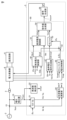
- Fig. 1 is a diagram showing a configuration example of a power conversion device 100.
- the power conversion device 100 is connected between an AC system 2 and a DC circuit 4.
- the DC circuit 4 includes an electric storage element connected to a DC terminal of a power converter 6.
- the electric storage element is, for example, an electric double layer capacitor or an electric storage device including a storage battery such as a lithium ion battery.
- the DC circuit 4 includes a DC terminal of another power converter connected to the DC terminal of the power converter 6.
- a BTB (Back To Back) system for connecting AC power systems having different rated frequencies, etc. is configured by linking two power converters.
- the power conversion device 100 includes a self-excited power converter 6 and a control device 5 for controlling the power converter 6.
- the power converter 6 is configured with a modular multilevel converter (MMC) including multiple converter cells (corresponding to the "cells” in FIG. 1) 1 connected in series with each other.
- MMC modular multilevel converter
- the "converter cell” is also called a “sub module” or “unit converter.”
- the power converter 6 is connected to the DC circuit 4 and performs power conversion between the DC circuit 4 and the AC system 2. Specifically, the power converter 6 converts the DC power output from the DC circuit 4 into AC power and outputs the AC power to the AC system 2 via the transformer 3. The power converter 6 also converts the AC power from the AC system 2 into DC power and outputs the DC power to the DC circuit 4.
- the power converter 6 is controlled by the control device 5 as a voltage source capable of outputting an AC voltage with a voltage phase and voltage amplitude different from the system voltage.
- the power converter 6 includes multiple arms for each phase of the AC system 2.
- the power converter 6 includes multiple leg circuits 8u, 8v, 8w (hereinafter, collectively referred to as "leg circuits 8" when referring to any one of them) connected in parallel between a positive DC terminal (i.e., high-potential DC terminal) Np and a negative DC terminal (i.e., low-potential DC terminal) Nn.
- leg circuits 8 when referring to any one of them connected in parallel between a positive DC terminal (i.e., high-potential DC terminal) Np and a negative DC terminal (i.e., low-potential DC terminal) Nn.
- the leg circuits 8 are provided for each of the multiple phases that make up the AC.
- the leg circuits 8 are connected between the AC system 2 and the DC circuit 4, and perform power conversion between the two circuits.
- Figure 1 shows a case where the AC system 2 is a three-phase AC system, and three leg circuits 8u, 8v, and 8w are provided corresponding to the u-phase, v-phase, and w-phase, respectively. Note that when the AC system 2 is a single-phase AC system, two leg circuits are provided.
- the AC terminals Nu, Nv, and Nw provided on the leg circuits 8u, 8v, and 8w, respectively, are connected to the AC system 2 via the transformer 3.
- the AC system 2 is, for example, an AC power system including an AC power source.
- FIG. 1 to facilitate illustration, the connection between the AC terminals Nv and Nw and the transformer 3 is not shown.
- the DC terminals provided in common to each leg circuit 8 i.e., the positive DC terminal Np and the negative DC terminal Nn) are connected to the DC circuit 4.
- the leg circuits 8u, 8v, 8w may be configured to be connected to the AC system 2 via an interconnection reactor.
- the leg circuits 8u, 8v, 8w may each be provided with a primary winding, and the leg circuits 8u, 8v, 8w may be AC-connected to the transformer 3 or the interconnection reactor via a secondary winding that is magnetically coupled to the primary winding.
- the primary winding may be the reactors 7a, 7b described below.
- leg circuit 8 is electrically (i.e., DC or AC) connected to the AC system 2 via a connection provided in each leg circuit 8u, 8v, 8w, such as the AC terminals Nu, Nv, Nw or the above-mentioned primary winding.
- the leg circuit 8u is divided into a positive arm 13u from the positive DC terminal Np to the AC terminal Nu, and a negative arm 14u from the negative DC terminal Nn to the AC terminal Nu.
- the connection point between the positive arm 13u and the negative arm 14u is connected to the transformer 3 as the AC terminal Nu.
- the positive DC terminal Np and the negative DC terminal Nn are connected to the DC circuit 4.
- the leg circuit 8v includes a positive arm 13v and a negative arm 14v
- the leg circuit 8w includes a positive arm 13w and a negative arm 14w.
- the leg circuits 8v and 8w have the same configuration as the leg circuit 8u, so the following description will be given using the leg circuit 8u as a representative.
- the positive arm 13u includes a plurality of converter cells 1 connected in cascade to each other and a reactor 7a.
- the plurality of converter cells 1 and the reactor 7a are connected in series to each other.
- the negative arm 14u includes a plurality of converter cells 1 connected in cascade to each other and a reactor 7b.
- the plurality of converter cells 1 and the reactor 7b are connected in series to each other.
- the reactor 7a may be inserted at any position in the positive arm 13u, and the reactor 7b may be inserted at any position in the negative arm 14u. There may be multiple reactors 7a and multiple reactors 7b. The inductance values of the reactors may be different from each other. Furthermore, only the reactor 7a in the positive arm 13u or only the reactor 7b in the negative arm 14u may be provided.
- the power conversion device 100 further includes an AC voltage detector 10, an AC current detector 15, DC voltage detectors 11a and 11b, and arm current detectors 9a and 9b provided in each leg circuit 8. These detectors measure electrical quantities (i.e., current, voltage) used to control the power conversion device 100. Signals detected by these detectors are input to the control device 5.
- the AC voltage detector 10 detects three-phase AC voltages Vsysu, Vsysv, and Vsysw (hereinafter collectively referred to as "AC voltage Vsys").
- the AC current detector 15 detects three-phase AC currents Isysu, Isysv, and Isysw (hereinafter collectively referred to as "AC current Isys") of the AC system 2.
- the DC voltage detector 11a detects the actual DC voltage Vdcp of the positive DC terminal Np connected to the DC circuit 4.
- the DC voltage detector 11b detects the actual DC voltage Vdcn of the negative DC terminal Nn connected to the DC circuit 4.
- the arm current detectors 9a and 9b provided in the leg circuit 8u for the u phase detect the measured positive arm current Iup flowing in the positive arm 13u and the measured negative arm current Iun flowing in the negative arm 14u.
- the arm current detectors 9a and 9b provided in the leg circuit 8v for the v phase detect the measured positive arm current Ivp and the measured negative arm current Ivn.
- the arm current detectors 9a and 9b provided in the leg circuit 8w for the w phase detect the measured positive arm current Iwp and the measured negative arm current Iwn.
- the DC current output from the power converter 6 (hereinafter also referred to as "output DC current Idc") is detected using a DC current detector not shown.
- the output DC current Idc corresponds to the value of the DC current flowing between the power converter 6 and the DC circuit 4.
- the output DC current Idc may be calculated as shown in the following formula (1) using the measured positive arm current values Iup, Ivp, Iwp and the measured negative arm current values Iun, Ivn, Iwn.
- FIG. 2 is a circuit diagram showing an example of the converter cell 1.
- the converter cell 1 shown in Fig. 2(a) has a circuit configuration called a half-bridge configuration. This converter cell 1 has two switching
- the power supply includes a series body formed by connecting elements 31p and 31n in series, a capacitor 32 as a power storage element, and a voltage detector 33. The series body and the capacitor 32 are connected in parallel.
- the voltage detector 33 detects the capacitance of the capacitor 32, a voltage Vcap is detected.
- the converter cell 1 shown in FIG. 2(b) has a circuit configuration called a full-bridge configuration.
- This converter cell 1 includes a first series body formed by connecting two switching elements 31p1 and 31n1 in series, a second series body formed by connecting two switching elements 31p2 and 31n2 in series, a capacitor 32, and a voltage detector 33.
- the first series body, the second series body, and the capacitor 32 are connected in parallel.
- the voltage detector 33 detects the voltage Vcap.
- the two switching elements 31p and 31n in FIG. 2(a) and the four switching elements 31p1, 31n1, 31p2, and 31n2 in FIG. 2(b) are configured by connecting a freewheel diode in inverse parallel to a self-extinguishing semiconductor switching element such as an IGBT (Insulated Gate Bipolar Transistor) or a MOSFET (Metal Oxide Semiconductor Field-Effect Transistor).
- a capacitor such as a film capacitor is mainly used for the capacitor 32.
- switching elements 31p, 31n, 31p1, 31n1, 31p2, and 31n2 are also collectively referred to as switching element 31. Furthermore, the on/off of the semiconductor switching element within switching element 31 is simply referred to as "on/off of switching element 31.”
- both terminals of switching element 31n are input/output terminals G1, G2.
- the voltage across capacitor 32 and zero voltage are output by the switching operation of switching elements 31p and 31n. For example, when switching element 31p is on and switching element 31n is off, the voltage across capacitor 32 is output. When switching element 31p is off and switching element 31n is on, zero voltage is output.
- Converter cell 1 shown in FIG. 2(b) outputs a positive voltage or zero voltage by turning on switching element 31n2, turning off switching element 31p2, and alternately turning on switching elements 31p1 and 31n1.
- Converter cell 1 shown in FIG. 2(b) can also output a zero voltage or negative voltage by turning off switching element 31n2, turning on switching element 31p2, and alternately turning on switching elements 31p1 and 31n1.
- the converter cell 1 may be configured as a half-bridge cell as shown in FIG. 2(a) or as a full-bridge cell as shown in FIG. 2(b).
- a converter cell other than the configurations shown above may be used, for example, a converter cell that uses a circuit configuration also known as a 1.5 half-bridge configuration in which the switching element 31p2 in FIG. 2(b) is replaced with only a diode.
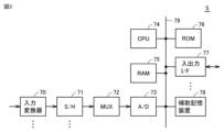
- FIG. 3 is a block diagram showing an example of a hardware configuration of the control device 5.
- the control device 5 in FIG. 3 is configured based on a computer.
- the control device 5 includes one or more input converters 70, one or more sample-and-hold (S/H) circuits 71, a multiplexer (MUX) 72, and an A/D converter 73.
- the control device 5 includes one or more central processing units (CPUs) 74, a random access memory (RAM) 75, and a read-only memory (ROM) 76.
- the control device 5 includes one or more input/output interfaces 77, an auxiliary storage device 78, and a bus 79 that connects the above components to each other.
- the input converter 70 includes an auxiliary transformer for each input channel.
- Each auxiliary transformer converts the detection signal from each electrical quantity detector in FIG. 1 into a signal with a voltage level suitable for subsequent signal processing.
- a sample-and-hold circuit 71 is provided for each input converter 70.
- the sample-and-hold circuit 71 samples and holds the signal representing the electrical quantity received from the corresponding input converter 70 at a specified sampling frequency.
- the multiplexer 72 sequentially selects the signals held in the multiple sample-and-hold circuits 71.
- the A/D converter 73 converts the signal selected by the multiplexer 72 into a digital value. Note that by providing multiple A/D converters 73, A/D conversion may be performed in parallel on the detection signals of multiple input channels.
- the CPU 74 controls the entire control device 5 and executes arithmetic processing according to a program.
- the RAM 75 as a volatile memory
- the ROM 76 as a non-volatile memory are used as the main memory of the CPU 74.
- the ROM 76 stores programs and setting values for signal processing.
- the auxiliary storage device 78 is a non-volatile memory with a larger capacity than the ROM 76, and stores programs, data on detected electrical quantity values, etc.
- the input/output interface 77 is an interface circuit for communication between the CPU 74 and external devices.
- control device 5 may be configured using circuits such as an FPGA (Field Programmable Gate Array) and an ASIC (Application Specific Integrated Circuit).
- control device 5 may be configured using analog circuits.
- Embodiment 1 is a diagram showing an example of a functional configuration of the control device 5 according to the first embodiment.
- the control device 5 includes a coordinate conversion unit 21, a frequency detection unit 22, an AC power calculation unit 24, an active power control unit 40, a capacitor voltage control unit 45, a reference voltage command generation unit 47, a voltage command generation unit 50, and a signal generation unit 58.
- Each of these functions is realized by a processing circuit.
- the processing circuit may be dedicated hardware, or may be a CPU that executes a program stored in the internal memory of the control device 5.
- the processing circuit is configured, for example, by an FPGA, an ASIC, or a combination of these.
- the coordinate conversion unit 21 uses the reference phase ⁇ c to perform three-phase/two-phase conversion of the AC currents Isysu, Isysv, and Isysw to calculate the d-axis current Id and the q-axis current Iq.
- the coordinate conversion unit 21 also uses the reference phase ⁇ c to perform three-phase/two-phase conversion of the AC voltages Vsysu, Vsysv, and Vsysw to calculate the d-axis voltage Vd and the q-axis voltage Vq.
- the frequency detection unit 22 detects the system angular frequency ⁇ sys of the AC voltages Vsysu, Vsysv, and Vsysw.
- the AC power calculation unit 24 calculates the active power P and reactive power Q of the AC system 2 based on the d-axis current Id, the q-axis current Iq, the d-axis voltage Vd, and the q-axis voltage Vq.
- the active power P and reactive power Q correspond to the detected value of the active power and the detected value of the reactive power output from the power converter 6 to the AC system 2, respectively. Therefore, in the following description, the above active power P and reactive power Q are also referred to as the active power detection value P and reactive power detection value Q of the AC system 2, respectively.
- the active power control unit 40 generates a reference phase ⁇ c0 of the AC voltage (hereinafter also simply referred to as "output AC voltage") output from the power converter 6 based on the active power detection value P, the active power command value P*, and the system angular frequency ⁇ sys of the AC system 2.
- the active power command value P* is, for example, a command value in response to a request from a higher-level device, a command value set by the system operator, or a command value as a frequency adjustment amount equivalent to governor-free operation of a synchronous generator when the frequency of the AC system 2 fluctuates.
- the active power control unit 40 also generates a DC current command value Idc*, which is a command value for the DC current output from the power converter 6, based on the active power detection value P and the output DC voltage Vdc of the power converter 6.
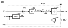
- FIG. 5 is a diagram showing a first example configuration of the active power control unit 40 according to the first embodiment.
- the active power control unit 40 according to the first example configuration generates a reference phase ⁇ c0 by a droop control method based on the active power detection value P, the active power command value P*, and the system angular frequency ⁇ sys of the AC system 2.
- the active power control unit 40 according to the first example configuration includes a proportional unit 401, a subtractor 402, an integrator 403, a divider 404, a low-pass filter 405, and an adder 406.
- the low-pass filter 405 outputs a value Pf obtained by removing high-frequency components from the active power detection value P.
- the low-pass filter 405 is, for example, a first-order lag element.
- the subtractor 402 outputs the difference between the active power command value P* and the value Pf obtained by removing high-frequency components from the active power (i.e., P*-Pf). Note that if the AC power calculation unit 24 uses a low-pass filter when calculating the active power detection value P, the low-pass filter 405 does not need to be provided.
- the proportional unit 401 outputs the multiplication value "Kd x (P* - Pf)" of the output value of the subtractor 402 and the coefficient Kd.
- the multiplication value "Kd x (P* - Pf)" is the angular frequency ⁇ cnv for correcting the system angular frequency ⁇ sys.
- the coefficient Kd is a coefficient that indicates the slope of the frequency droop characteristics.
- the adder 406 outputs the angular frequency ⁇ cnv, which is the system frequency ⁇ sys plus the angular frequency ⁇ cnv, to the integrator 403.
- the integrator 403 generates the reference phase ⁇ c0 by time-integrating the output value of the adder 406.
- the divider 404 generates the DC current command value Idc* by dividing the active power detection value P by the output DC voltage Vdc.
- FIG. 6 is a diagram showing a second example configuration of the active power control unit 40 according to the first embodiment.
- the active power control unit 40 according to the second example configuration generates the reference phase ⁇ c0 by simulating the characteristics of a synchronous generator based on the active power detection value P and the active power command value P*.
- the active power control unit 40 according to the second example configuration includes a divider 404, an adder/subtractor 411, an integrator 412, a high-pass filter 413, a proportional unit 414, an adder 415, and an integrator 416.
- the method of generating the DC current command value Idc* by the divider 404 is the same as that described in FIG. 5.
- the integrator 412 integrates the output value of the adder/subtractor 411 over time to output the angular frequency deviation ⁇ .
- "M" of the integrator 412 is the inertia constant of the synchronous generator.
- the angular frequency deviation ⁇ output by the integrator 412 corresponds to the difference between the angular frequency of the rotor in the virtual synchronous generator and the reference angular frequency ⁇ sys0.
- the reference angular frequency ⁇ sys0 is the angular frequency of the reference frequency of power in the AC system 2 (for example, 50 Hz or 60 Hz).
- the high-pass filter 413 performs high-pass filtering on the angular frequency deviation ⁇ and outputs the result to the proportional converter 414.
- the proportional converter 414 outputs the multiplied value "D ⁇ " of the angular frequency deviation ⁇ after high-pass filtering and the damping constant D.
- the integrator 412 integrates the output value of the adder-subtracter 411 over time. This simulates the braking force of the synchronous generator in the control of the power converter 6.
- the integrator 416 integrates the angular frequency ⁇ over time to generate the reference phase ⁇ c0.
- the capacitor voltage control unit 45 generates a reference phase correction value ⁇ c for correcting the reference phase ⁇ c0 based on the capacitor voltage command value Vcap* and the voltage Vcap of the capacitor included in the power converter 6.
- the capacitor voltage command value Vcap* is a command value given for the average voltage value of all the capacitors included in the power converter 6.
- the capacitor voltage control unit 45 generates the reference phase correction value ⁇ c so that the average voltage value of all the capacitors follows the capacitor voltage command value Vcap*.
- the capacitor voltage control unit 45 can be configured, for example, as a PI controller, a PID controller, or another controller used for feedback control.
- the reference voltage command generator 47 generates the reference voltage command values Vd* and Vq* based on the d-axis voltage Vd, the q-axis voltage Vq, the reactive power detection value Q, and the reactive power command value Q*.
- FIG. 7 is a diagram showing an example of the configuration of the reference voltage command generating unit 47.
- the reference voltage command generating unit 47 includes a positive-phase voltage calculating unit 36, subtractors 37 and 38, a voltage adjusting unit 91, coordinate conversion units 92 and 94, and an adder 93.
- the positive-sequence voltage calculation unit 36 calculates the positive-sequence voltage Vpos based on the d-axis voltage Vd and the q-axis voltage Vq.
- the voltage adjustment unit 91 selects either the automatic reactive power adjustment mode or the automatic voltage adjustment mode, and generates a voltage amplitude adjustment amount ⁇ Vacref based on the selected mode. Specifically, when the automatic reactive power adjustment mode is selected, the voltage adjustment unit 91 generates a voltage amplitude adjustment amount ⁇ Vacref by feedback control for making the deviation ⁇ Q equal to or less than a specified value (e.g., 0). When the automatic voltage adjustment mode is selected, the voltage adjustment unit 91 generates a voltage amplitude adjustment amount ⁇ Vacref by feedback control for making the deviation ⁇ Vpos equal to or less than a specified value (e.g., 0).
- the voltage adjustment unit 91 is composed of a PI controller, a first-order lag element, etc.
- the coordinate conversion unit 92 converts the d-axis component of the specified voltage command value (i.e., the specified d-axis voltage command value Vdx) and the q-axis component (i.e., the specified q-axis voltage command value Vqx) into an amplitude
- the specified d-axis voltage command value Vdx and the specified q-axis voltage command value Vqx are values that are set in advance by a system operator or the like.
- the adder 93 adds the amplitude
- the coordinate conversion unit 94 performs dq-axis conversion of the amplitude
- the voltage command generating unit 50 generates a voltage command value for controlling the first active power on the DC side exchanged between the DC circuit 4 and the power converter 6 and for controlling the second active power on the AC side exchanged between the AC system 2 and the power converter 6 based on the output DC current Idc of the power converter 6, the DC current command value Idc*, the reference voltage command values Vd*, Vq* of the output AC voltage of the power converter 6, the reference phase ⁇ c0, and the reference phase correction value ⁇ c.
- the voltage command generating unit 50 includes a DC current control unit 51, an adder 52, a coordinate conversion unit 53, and a command value generating unit 54.
- the DC current control unit 51 generates a DC voltage command value Vdc* for controlling the first active power on the DC side based on the DC current command value Idc* and the output DC current Idc. Specifically, the DC current control unit 51 generates a DC voltage command value Vdc* so that the output DC current Idc follows the DC current command value Idc*. According to such a DC voltage command value Vdc*, the output DC current Idc is controlled so as to follow the DC current command value Idc*, and as a result, the first active power on the DC side is appropriately controlled.
- the DC current control unit 51 can be configured, for example, as a PI controller, a PID controller, or another controller used for feedback control.
- the adder 52 adds the reference phase ⁇ c0 and the reference phase correction value ⁇ c to output the reference phase ⁇ c.
- the reference phase ⁇ c is the reference phase ⁇ c0 corrected by the reference phase correction value ⁇ c.
- the reference phase ⁇ c reflects the control amount required to control the second active power on the AC side and the control amount required to control the capacitor voltage.
- the coordinate conversion unit 53 generates an AC voltage command value Vac* for controlling the second active power on the AC side based on the reference phase ⁇ c and the reference voltage command values Vd*, Vq*. Specifically, the coordinate conversion unit 53 performs two-phase/three-phase conversion of the reference voltage command values Vd*, Vq* on the d-q axes using the reference phase ⁇ c to generate three-phase AC voltage command values Vacu*, Vacv*, Vacw* (i.e., AC voltage command value Vac*). Thus, the coordinate conversion unit 53 functions as an "AC voltage command generation unit" that generates the AC voltage command value Vac*.
- the AC voltage command value Vac* is generated using a reference phase ⁇ c that reflects the control amount required for controlling the active power on the AC side and the control amount required for controlling the capacitor voltage. Therefore, according to such an AC voltage command value Vac*, the second active power on the AC side is appropriately controlled, and the capacitor voltage is also appropriately controlled.
- the command value generating unit 54 generates a voltage command value Vcnv* based on the DC voltage command value Vdc* and the AC voltage command value Vac*.
- the command value generating unit 54 generates voltage command values for the positive arm and negative arm of each phase based on the AC voltage command values Vacu*, Vacv*, Vacw* and the DC voltage command value Vdc*.
- the voltage command value for the positive arm 13u of the U phase is a value obtained by subtracting the AC voltage command value Vacu* from the DC voltage command value Vdc*.
- the voltage command value for the negative arm 14u of the U phase is a value obtained by adding the AC voltage command value Vacu* to the DC voltage command value Vdc*.
- the voltage command values for the positive arm and negative arm of the V phase and W phase are generated in a similar manner.
- the command value generator 54 generates the voltage command values Vucnv*, Vvcnv*, and Vwcnv* (i.e., the voltage command value Vcnv*) of the converter cell 1 of each phase based on the voltage command values of the positive arm and negative arm of each phase.
- the signal generating unit 58 generates a control signal for the power converter 6 based on the voltage command value Vcnv*. Specifically, the signal generating unit 58 executes PWM (Pulse Width Modulation) control based on the voltage command values Vucnv*, Vvcnv*, and Vwcnv* to generate a gate signal GP that controls the on/off driving of the switching element 31 of each converter cell 1 of each phase.
- PWM Pulse Width Modulation
- the signal generating unit 58 generates a PWM modulated signal by comparing the voltage of the voltage command value Vucnv* with a carrier signal CS from a carrier generator (not shown).
- the carrier signal CS is composed of a periodic signal such as a triangular wave.
- the PWM modulation signal When the voltage of the voltage command value Vucnv* is higher than the voltage of the carrier signal CS, the PWM modulation signal is set to a high level. Conversely, when the voltage of the carrier signal CS is higher than the output voltage command value Vucnv*, the PWM modulation signal is set to a low level.
- the carrier signal CS is generated so as to shift the timing of the PWM signals between the N converter cells 1 of each phase to achieve phase-shift PWM control.
- the signal generating unit 58 also generates the voltage command value Vvcnv* for each V-phase converter cell 1 and the voltage command value Vwcnv* for each W-phase converter cell 1 in the same manner as described above. As a result, the signal generating unit 58 generates a gate signal GP that controls the on/off of each of the switching elements 31 included in the converter cell 1 based on the PWM modulated signal. Each switching element 31 of each converter cell 1 is driven on and off according to the gate signal GP.
- the DC voltage command value Vdc* is generated so that the output DC current Idc follows the DC current command value Idc* generated by the active power control unit 40.
- the AC voltage command value Vac* is generated using a reference phase ⁇ c based on the reference phase ⁇ c0 generated by the active power control unit 40 and the reference phase correction value ⁇ c generated by the capacitor voltage control unit 45. This allows the second active power on the AC side and the capacitor voltage to be appropriately controlled. Therefore, by appropriately controlling the active powers on the DC side and AC side, the power converter 6 can continue stable operation.
- the capacitor voltage can be controlled by exchanging power on the AC side, so the power converter 6 can continue to operate stably.
- Fig. 8 is a diagram showing an example of a functional configuration of a control device 5A according to the embodiment 2.
- the control device 5A corresponds to the control device 5 in Fig. 1, but is denoted by the symbol "A" for convenience in order to distinguish it from the control device 5 according to the embodiment 1. This also applies to the following embodiment 3.
- the control device 5A includes a coordinate conversion unit 21, a frequency detection unit 22, an amplitude calculation unit 23, an AC power calculation unit 24, an active power control unit 41, a capacitor voltage control unit 45, a reference voltage command generation unit 47, a voltage command generation unit 50A, and a signal generation unit 58.
- the components other than the amplitude calculation unit 23, the active power control unit 41, and the voltage command generation unit 50A are the same as those described in FIG. 4, and therefore detailed description thereof will not be repeated.
- the amplitude calculation unit 23 calculates a voltage amplitude Vmag, which is the amplitude of the d-axis voltage Vd and the q-axis voltage Vq. Specifically, the amplitude calculation unit 23 removes high-frequency components from the d-axis voltage Vd and the q-axis voltage Vq using a moving average filter or the like, and calculates the sum of the squares of the removed d-axis voltage Vd and q-axis voltage Vq (i.e., ( Vd2 + Vq2 ) 1/2 ). The amplitude calculation unit 23 outputs the sum of the squares as the voltage amplitude Vmag of the output AC voltage of the power converter 6.
- the active power control unit 41 generates a reference phase ⁇ c based on the active power detection value P, the active power command value P*, and the system angular frequency ⁇ sys of the AC system 2.
- the second embodiment differs from the first embodiment in that the reference phase generated by the active power control unit 41 is " ⁇ c" (i.e., the reference phase is not corrected using the reference phase correction value ⁇ c).
- FIG. 9 is a diagram showing a first example configuration of the active power control unit 41 according to the second embodiment.
- the active power control unit 41 generates a reference phase ⁇ c by a droop control method based on the active power detection value P, the active power command value P*, and the system angular frequency ⁇ sys of the AC system 2.
- the active power control unit 41 according to the first example configuration includes a proportional unit 401, a subtractor 402, an integrator 403, a low-pass filter 405, and an adder 406. That is, the active power control unit 41 according to the first example configuration corresponds to a configuration in which the divider 404 is deleted from the active power control unit 40 according to the first example configuration shown in FIG. 5.
- the functions of the proportional unit 401, the subtractor 402, the integrator 403, the low-pass filter 405, and the adder 406 are similar to those described in FIG. 5, and therefore detailed description thereof will not be repeated.
- the integrator 403 of the active power control unit 41 outputs the reference phase ⁇ c.
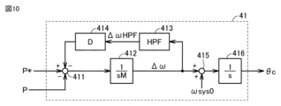
- FIG. 10 is a diagram showing a second example of the configuration of the active power control unit 41 according to the second embodiment.
- the active power control unit 41 according to the second example generates the reference phase ⁇ c by simulating the characteristics of a synchronous generator based on the active power detection value P and the active power command value P*.
- the active power control unit 41 according to the second example includes an adder-subtractor 411, an integrator 412, a high-pass filter 413, a proportional unit 414, an adder 415, and an integrator 416. That is, the active power control unit 41 according to the second example of the configuration corresponds to a configuration in which the divider 404 is deleted from the active power control unit 40 according to the second example of the configuration shown in FIG. 6.
- the functions of the adder/subtractor 411, the integrator 412, the high-pass filter 413, the proportional unit 414, the adder 415, and the integrator 416 are similar to those described in FIG. 6, and therefore detailed description thereof will not be repeated.
- the integrator 416 of the active power control unit 41 outputs the reference phase ⁇ c.
- the voltage command generating unit 50A generates voltage command values for controlling the first active power on the DC side and the second active power on the AC side based on the output DC current Idc, the reference voltage command values Vd*, Vq*, the reference phase ⁇ c, and the DC current command value Idc* obtained by converting the reference phase correction value ⁇ c.
- the voltage command generating unit 50A includes a DC current control unit 51, a coordinate conversion unit 53, a command value generating unit 54, and a phase conversion unit 55.
- the phase conversion unit 55 generates the DC current command value Idc* based on the reference phase correction value ⁇ c, the output DC voltage Vdc, and the voltage amplitude Vmag, which is the amplitude value of the output AC voltage of the power converter 6.
- FIG. 11 is a diagram showing an example of the configuration of the phase conversion unit 55 according to the second embodiment.
- the phase conversion unit 55 includes an arithmetic unit 501, a divider 502, a multiplier 503, and a sine arithmetic unit 504.
- the sine calculator 504 generates sin( ⁇ c) based on the reference phase correction value ⁇ c.
- the calculator 501 calculates the multiplication value (i.e., sin( ⁇ c) ⁇ Vn/Xs) of the value obtained by dividing the rated voltage Vn of the AC system 2 by the inductance Xs of the power converter 6 (i.e., Vn/Xs) and sin( ⁇ c).
- the divider 502 outputs the value obtained by dividing the value output from the calculator 501 by the output DC voltage Vdc (i.e., sin( ⁇ c) ⁇ Vn/(Xs ⁇ Vdc)).
- the multiplier 503 outputs the value obtained by multiplying the value output from the divider 502 by the voltage amplitude Vmag (i.e., Vmag ⁇ sin( ⁇ c) ⁇ Vn/(Xs ⁇ Vdc)) as the DC current command value Idc*.
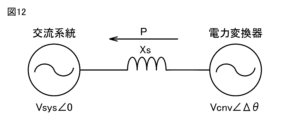
- FIG. 12 is a diagram for explaining a method of converting a reference phase correction value into a DC current command value.
- the active power output from the power converter 6 is P
- the AC voltage of the AC system 2 is Vsys
- the output AC voltage of the power converter 6 is Vcnv
- the phase difference between the AC voltage of the AC system 2 and the output AC voltage of the power converter 6 is ⁇
- the inductance of the power converter 6 is Xs.
- the DC current command value Idc* is calculated by the configuration of the phase conversion unit 55 in FIG. 11. This conversion process allows the control amount (e.g., the reference phase correction value ⁇ c) required for the capacitor voltage control by the capacitor voltage control unit 45 to be reflected in the DC current command value Idc*.
- the control amount e.g., the reference phase correction value ⁇ c
- the DC current control unit 51 generates a DC voltage command value Vdc* so that the output DC current Idc follows the DC current command value Idc*. According to such a DC voltage command value Vdc*, the output DC current Idc is controlled so as to follow the DC current command value Idc*, and as a result, the first active power on the DC side is appropriately controlled.
- the DC current command value Idc* is obtained by converting the reference phase correction value ⁇ c generated by the capacitor voltage control unit 45. Therefore, the DC current command value Idc* reflects the control amount required for capacitor voltage control. Therefore, the capacitor voltage is also appropriately controlled according to such a DC voltage command value Vdc*.
- the coordinate conversion unit 53 generates an AC voltage command value Vac* for controlling the second active power on the AC side based on the reference phase ⁇ c and the reference voltage command values Vd* and Vq* generated by the active power control unit 41.
- the AC voltage command value Vac* is generated using a reference phase ⁇ c that reflects the control amount required for active power control. Therefore, the second active power on the AC side is appropriately controlled by such an AC voltage command value Vac*.
- the command value generator 54 generates a voltage command value Vcnv* based on the DC voltage command value Vdc* and the AC voltage command value Vac*.
- the signal generator 58 generates a gate signal GP for the power converter 6 based on the voltage command value Vcnv*.
- the DC voltage command value Vdc* is generated so that the output DC current Idc follows the DC current command value Idc* obtained by converting the reference phase correction value ⁇ c generated by the capacitor voltage control unit 45.
- the AC voltage command value Vac* is generated using the reference phase ⁇ c generated by the active power control unit 41. This allows the second active power on the AC side to be appropriately controlled. Therefore, by appropriately controlling the active powers on the DC side and AC side, the power converter 6 can continue stable operation.
- the capacitor voltage can be controlled by exchanging power on the DC side, so the power converter 6 can continue to operate stably.
- Fig. 13 is a diagram showing an example of a functional configuration of a control device 5B according to the third embodiment.
- the control device 5B includes a coordinate conversion unit 21, a frequency detection unit 22, an amplitude calculation unit 23, an AC power calculation unit 24, an active power control unit 42, a capacitor voltage control unit 45, a reference voltage command generation unit 47, a voltage command generation unit 50B, and a signal generation unit 58.
- the components other than the active power control unit 42 and the voltage command generation unit 50B are similar to those described in Fig. 8, and therefore detailed description thereof will not be repeated.
- the reference phase correction value output from the capacitor voltage control unit 45 is set to " ⁇ c0" for convenience of description.
- the active power control unit 42 generates a reference phase ⁇ c based on the active power detection value P, the active power command value P*, and the system angular frequency ⁇ sys of the AC system 2.
- the active power control unit 42 is similar to the active power control unit 41 according to the second embodiment.
- the active power control unit 42 further calculates a phase adjustment amount based on the detection value of the active power output from the power converter 6 to the AC system 2, using the active power detection value P and the voltage amplitude Vmag of the output AC voltage of the power converter 6.
- the active power control unit 42 generates a reference phase ⁇ c by a droop control method based on the active power detection value P, the active power command value P*, and the system angular frequency ⁇ sys of the AC system 2.
- the active power control unit 42 according to the first example of the configuration includes a proportional unit 401, a subtractor 402, an integrator 403, a low-pass filter 405, an adder 406, a calculator 407, a divider 408, and an arcsine calculator 409.
- the active power control unit 42 according to the first example of the configuration corresponds to a configuration in which the calculator 407, the divider 408, and the arcsine calculator 409 are added to the active power control unit 41 according to the first example of the configuration shown in FIG. 9.
- the functions of the proportional unit 401, subtractor 402, integrator 403, low-pass filter 405, and adder 406 are similar to those described in FIG. 5, and therefore detailed description thereof will not be repeated.
- the integrator 403 of the active power control unit 42 outputs the reference phase ⁇ c.
- the calculator 407 outputs the multiplication value (i.e., P ⁇ Xs/Vn) of the active power detection value P and the value (i.e., Xs/Vn) obtained by dividing the inductance Xs of the power converter 6 by the rated voltage Vn of the AC system 2.
- the divider 408 outputs the value (i.e., P ⁇ Xs/(Vn ⁇ Vmag)) obtained by dividing the output value of the calculator 407 by the voltage amplitude Vmag of the output AC voltage of the power converter 6.
- the arcsine calculator 409 generates the arcsine (P ⁇ Xs/(Vn ⁇ Vmag)) calculated based on the output value of the divider 408 as the phase adjustment amount ⁇ c1.
- the active power control unit 42 according to the second example of the configuration generates the reference phase ⁇ c by simulating the characteristics of a synchronous generator based on the active power detection value P and the active power command value P*.
- the active power control unit 42 according to the second example of the configuration includes a calculator 407, a divider 408, an arcsine calculator 409, an adder/subtractor 411, an integrator 412, a high-pass filter 413, a proportional unit 414, an adder 415, and an integrator 416.
- the active power control unit 42 according to the second example of the configuration corresponds to a configuration in which the calculator 407, the divider 408, and the arcsine calculator 409 are added to the active power control unit 41 according to the second example of the configuration shown in FIG. 10.
- the functions of the adder/subtractor 411, integrator 412, high-pass filter 413, proportional unit 414, adder 415, and integrator 416 are similar to those described in FIG. 6, and therefore detailed description thereof will not be repeated.
- the integrator 416 of the active power control unit 42 outputs the reference phase ⁇ c.
- the functions of the calculator 407, divider 408, and arcsine calculator 409 are similar to those described in FIG. 14. Therefore, the phase adjustment amount ⁇ c1 is generated by the same procedure as above.
- the voltage command generating unit 50B generates a voltage command value for controlling the first active power on the DC side and the second active power on the AC side based on the output DC current Idc, the reference voltage command values Vd*, Vq*, the reference phase ⁇ c, and the DC current command value Idc* obtained by converting the reference phase correction value ⁇ c.
- the voltage command generating unit 50B includes a DC current control unit 51, a coordinate conversion unit 53, a command value generating unit 54, a phase conversion unit 55, and an adder 57. That is, the voltage command generating unit 50B corresponds to a configuration in which an adder 57 is added to the voltage command generating unit 50A shown in FIG. 8.
- the adder 57 generates the reference phase correction value ⁇ c by adding the reference phase correction value ⁇ c0 output from the capacitor voltage control unit 45 and the phase adjustment amount ⁇ c1 output from the active power control unit 42. In this way, the phase adjustment amount ⁇ c1 is fed forward to the reference phase correction value ⁇ c0 based on the capacitor voltage control. Therefore, in the third embodiment, the reference phase correction value ⁇ c reflects the phase correction amount required for the capacitor voltage control and the phase adjustment amount calculated based on the detection value of the active power output from the power converter 6 to the AC system 2.
- the phase conversion unit 55 converts the reference phase correction value ⁇ c, which is the sum of the reference phase correction value ⁇ c0 and the phase adjustment amount ⁇ c1, into a DC current command value Idc* and outputs it to the DC current control unit 51.
- the DC current control unit 51 generates a DC voltage command value Vdc* so that the output DC current Idc follows the DC current command value Idc*. According to such a DC voltage command value Vdc*, the output DC current Idc is controlled to follow the DC current command value Idc*, and as a result, the first active power on the DC side is appropriately controlled.
- the DC current command value Idc* is obtained by converting the reference phase correction value ⁇ c, which is the sum of the reference phase correction value ⁇ c0 and the phase adjustment amount ⁇ c1. Therefore, the DC current command value Idc* reflects the control amount required for capacitor voltage control and the phase adjustment amount based on the detection value of the active power on the AC side. Therefore, such a DC voltage command value Vdc* allows for more appropriate control of the capacitor voltage.
- the coordinate conversion unit 53 generates an AC voltage command value Vac* for controlling the second active power on the AC side based on the reference phase ⁇ c and the reference voltage command values Vd* and Vq*.
- the second active power on the AC side is appropriately controlled by using this AC voltage command value Vac*.
- the command value generator 54 generates a voltage command value Vcnv* based on the DC voltage command value Vdc* and the AC voltage command value Vac*.
- the signal generator 58 generates a gate signal GP for the power converter 6 based on the voltage command value Vcnv*.
- the third embodiment has the following advantages. Specifically, the phase adjustment amount ⁇ c1 generated by the active power control unit 42 is fed forward to the reference phase correction value ⁇ c0, and the reference phase correction value ⁇ c, which is the sum of these, is converted to the DC current command value Idc*. Therefore, the output value of the active power control unit 42 (i.e., the phase adjustment amount ⁇ c1) can be quickly reflected in the control amount required for the capacitor voltage control.
- the capacitor voltage control reflecting the power difference is performed, so that the fluctuation of the capacitor voltage can be suppressed, and the power converter 6 can continue stable operation.
- the power converter 6 is configured as a modular multilevel converter, but is not limited to this configuration.
- the circuit system of the power converter 6 may be configured as a two-level converter that converts AC power into two-level DC power, or may be configured as a three-level converter that converts AC power into three-level DC power.
- the capacitor voltage control unit 45 generates a reference phase correction value ⁇ c based on a predetermined capacitor voltage command value Vcap* and the voltage Vcap of the capacitor included in the power converter 6.
Landscapes
- Engineering & Computer Science (AREA)
- Power Engineering (AREA)
- Inverter Devices (AREA)
Priority Applications (3)
| Application Number | Priority Date | Filing Date | Title |
|---|---|---|---|
| EP23927511.8A EP4683201A4 (en) | 2023-03-16 | 2023-03-16 | POWER CONVERSION DEVICE |
| JP2025506419A JPWO2024189892A1 (https=) | 2023-03-16 | 2023-03-16 | |
| PCT/JP2023/010301 WO2024189892A1 (ja) | 2023-03-16 | 2023-03-16 | 電力変換装置 |
Applications Claiming Priority (1)
| Application Number | Priority Date | Filing Date | Title |
|---|---|---|---|
| PCT/JP2023/010301 WO2024189892A1 (ja) | 2023-03-16 | 2023-03-16 | 電力変換装置 |
Publications (1)
| Publication Number | Publication Date |
|---|---|
| WO2024189892A1 true WO2024189892A1 (ja) | 2024-09-19 |
Family
ID=92754853
Family Applications (1)
| Application Number | Title | Priority Date | Filing Date |
|---|---|---|---|
| PCT/JP2023/010301 Ceased WO2024189892A1 (ja) | 2023-03-16 | 2023-03-16 | 電力変換装置 |
Country Status (3)
| Country | Link |
|---|---|
| EP (1) | EP4683201A4 (https=) |
| JP (1) | JPWO2024189892A1 (https=) |
| WO (1) | WO2024189892A1 (https=) |
Citations (6)
| Publication number | Priority date | Publication date | Assignee | Title |
|---|---|---|---|---|
| EP2790312A2 (en) * | 2013-04-11 | 2014-10-15 | General Electric Company | Power decoupling controller and method for power conversion system |
| WO2020240810A1 (ja) * | 2019-05-31 | 2020-12-03 | 東芝エネルギーシステムズ株式会社 | 電力変換装置 |
| WO2021213655A1 (en) | 2020-04-23 | 2021-10-28 | Abb Power Grids Switzerland Ag | Power supporting arrangement for a power grid operated as a virtual synchronous machine |
| JP2022056359A (ja) * | 2020-09-29 | 2022-04-08 | 三菱電機株式会社 | 電力変換装置 |
| JP7051028B1 (ja) * | 2021-09-28 | 2022-04-08 | 三菱電機株式会社 | 電力変換装置、および電力変換システム |
| JP7209908B1 (ja) * | 2022-05-30 | 2023-01-20 | 三菱電機株式会社 | 電力変換装置、および制御装置 |
Family Cites Families (2)
| Publication number | Priority date | Publication date | Assignee | Title |
|---|---|---|---|---|
| CN108964488B (zh) * | 2018-08-14 | 2021-01-19 | 中南大学 | 一种用于级联整流器的分层控制方法及系统 |
| CN110048455B (zh) * | 2019-04-24 | 2021-06-01 | 湖南大学 | 具有弱电网故障穿越能力的下垂控制逆变器及其控制方法 |
-
2023
- 2023-03-16 EP EP23927511.8A patent/EP4683201A4/en active Pending
- 2023-03-16 WO PCT/JP2023/010301 patent/WO2024189892A1/ja not_active Ceased
- 2023-03-16 JP JP2025506419A patent/JPWO2024189892A1/ja active Pending
Patent Citations (6)
| Publication number | Priority date | Publication date | Assignee | Title |
|---|---|---|---|---|
| EP2790312A2 (en) * | 2013-04-11 | 2014-10-15 | General Electric Company | Power decoupling controller and method for power conversion system |
| WO2020240810A1 (ja) * | 2019-05-31 | 2020-12-03 | 東芝エネルギーシステムズ株式会社 | 電力変換装置 |
| WO2021213655A1 (en) | 2020-04-23 | 2021-10-28 | Abb Power Grids Switzerland Ag | Power supporting arrangement for a power grid operated as a virtual synchronous machine |
| JP2022056359A (ja) * | 2020-09-29 | 2022-04-08 | 三菱電機株式会社 | 電力変換装置 |
| JP7051028B1 (ja) * | 2021-09-28 | 2022-04-08 | 三菱電機株式会社 | 電力変換装置、および電力変換システム |
| JP7209908B1 (ja) * | 2022-05-30 | 2023-01-20 | 三菱電機株式会社 | 電力変換装置、および制御装置 |
Non-Patent Citations (1)
| Title |
|---|
| See also references of EP4683201A1 |
Also Published As
| Publication number | Publication date |
|---|---|
| EP4683201A4 (en) | 2026-04-29 |
| JPWO2024189892A1 (https=) | 2024-09-19 |
| EP4683201A1 (en) | 2026-01-21 |
Similar Documents
| Publication | Publication Date | Title |
|---|---|---|
| EP4030612B1 (en) | Power conversion device | |
| JP7224565B1 (ja) | 電力変換装置、および制御装置 | |
| JP7183486B1 (ja) | 電力変換装置、および制御装置 | |
| JP7209908B1 (ja) | 電力変換装置、および制御装置 | |
| JP7126631B1 (ja) | 電力変換装置及び制御装置 | |
| US12549110B2 (en) | Power conversion device simulating a synchronous generator | |
| US12266935B2 (en) | Power conversion device | |
| JP5580377B2 (ja) | 静止型無効電力補償装置及び電圧制御方法 | |
| WO2024189892A1 (ja) | 電力変換装置 | |
| JP7051033B1 (ja) | 電力変換装置及び制御装置 | |
| WO2022259465A1 (ja) | 電力変換装置 | |
| JP7374395B1 (ja) | 電力変換システム | |
| JP7761156B2 (ja) | 制御装置、電力変換装置、電力変換装置の制御方法およびプログラム | |
| WO2025177422A1 (ja) | 電力変換装置 | |
| US12476469B2 (en) | Electric power control system simulating a synchronous generator | |
| JP5616412B2 (ja) | 単相電圧型交直変換装置 | |
| JP2026014458A (ja) | 電力変換装置 | |
| WO2025046684A1 (ja) | 電力変換装置 | |
| WO2025224780A1 (ja) | 電力変換装置 | |
| WO2023214462A1 (ja) | 電力変換装置 | |
| JPWO2024189892A5 (https=) | ||
| JP2025108030A (ja) | 制御回路、および、蓄電池システム | |
| JP2014072983A (ja) | 単相電圧型交直変換装置 |
Legal Events
| Date | Code | Title | Description |
|---|---|---|---|
| 121 | Ep: the epo has been informed by wipo that ep was designated in this application |
Ref document number: 23927511 Country of ref document: EP Kind code of ref document: A1 |
|
| ENP | Entry into the national phase |
Ref document number: 2025506419 Country of ref document: JP Kind code of ref document: A |
|
| WWE | Wipo information: entry into national phase |
Ref document number: 2025506419 Country of ref document: JP |
|
| WWE | Wipo information: entry into national phase |
Ref document number: 2023927511 Country of ref document: EP |
|
| NENP | Non-entry into the national phase |
Ref country code: DE |
|
| ENP | Entry into the national phase |
Ref document number: 2023927511 Country of ref document: EP Effective date: 20251016 |
|
| ENP | Entry into the national phase |
Ref document number: 2023927511 Country of ref document: EP Effective date: 20251016 |
|
| ENP | Entry into the national phase |
Ref document number: 2023927511 Country of ref document: EP Effective date: 20251016 |
|
| ENP | Entry into the national phase |
Ref document number: 2023927511 Country of ref document: EP Effective date: 20251016 |
|
| ENP | Entry into the national phase |
Ref document number: 2023927511 Country of ref document: EP Effective date: 20251016 |