WO2024189679A1 - 感光性樹脂組成物、感光性エレメント、硬化物、レジストパターンの形成方法、及び、プリント配線板の製造方法 - Google Patents
感光性樹脂組成物、感光性エレメント、硬化物、レジストパターンの形成方法、及び、プリント配線板の製造方法 Download PDFInfo
- Publication number
- WO2024189679A1 WO2024189679A1 PCT/JP2023/009338 JP2023009338W WO2024189679A1 WO 2024189679 A1 WO2024189679 A1 WO 2024189679A1 JP 2023009338 W JP2023009338 W JP 2023009338W WO 2024189679 A1 WO2024189679 A1 WO 2024189679A1
- Authority
- WO
- WIPO (PCT)
- Prior art keywords
- photosensitive resin
- mass
- resin composition
- meth
- resist pattern
- Prior art date
- Legal status (The legal status is an assumption and is not a legal conclusion. Google has not performed a legal analysis and makes no representation as to the accuracy of the status listed.)
- Ceased
Links
Images

Classifications
-
- G—PHYSICS
- G03—PHOTOGRAPHY; CINEMATOGRAPHY; ANALOGOUS TECHNIQUES USING WAVES OTHER THAN OPTICAL WAVES; ELECTROGRAPHY; HOLOGRAPHY
- G03F—PHOTOMECHANICAL PRODUCTION OF TEXTURED OR PATTERNED SURFACES, e.g. FOR PRINTING, FOR PROCESSING OF SEMICONDUCTOR DEVICES; MATERIALS THEREFOR; ORIGINALS THEREFOR; APPARATUS SPECIALLY ADAPTED THEREFOR
- G03F7/00—Photomechanical, e.g. photolithographic, production of textured or patterned surfaces, e.g. printing surfaces; Materials therefor, e.g. comprising photoresists; Apparatus specially adapted therefor
- G03F7/004—Photosensitive materials
- G03F7/027—Non-macromolecular photopolymerisable compounds having carbon-to-carbon double bonds, e.g. ethylenic compounds
- G03F7/028—Non-macromolecular photopolymerisable compounds having carbon-to-carbon double bonds, e.g. ethylenic compounds with photosensitivity-increasing substances, e.g. photoinitiators
- G03F7/031—Organic compounds not covered by group G03F7/029
-
- G—PHYSICS
- G03—PHOTOGRAPHY; CINEMATOGRAPHY; ANALOGOUS TECHNIQUES USING WAVES OTHER THAN OPTICAL WAVES; ELECTROGRAPHY; HOLOGRAPHY
- G03F—PHOTOMECHANICAL PRODUCTION OF TEXTURED OR PATTERNED SURFACES, e.g. FOR PRINTING, FOR PROCESSING OF SEMICONDUCTOR DEVICES; MATERIALS THEREFOR; ORIGINALS THEREFOR; APPARATUS SPECIALLY ADAPTED THEREFOR
- G03F7/00—Photomechanical, e.g. photolithographic, production of textured or patterned surfaces, e.g. printing surfaces; Materials therefor, e.g. comprising photoresists; Apparatus specially adapted therefor
- G03F7/004—Photosensitive materials
- G03F7/027—Non-macromolecular photopolymerisable compounds having carbon-to-carbon double bonds, e.g. ethylenic compounds
-
- G—PHYSICS
- G03—PHOTOGRAPHY; CINEMATOGRAPHY; ANALOGOUS TECHNIQUES USING WAVES OTHER THAN OPTICAL WAVES; ELECTROGRAPHY; HOLOGRAPHY
- G03F—PHOTOMECHANICAL PRODUCTION OF TEXTURED OR PATTERNED SURFACES, e.g. FOR PRINTING, FOR PROCESSING OF SEMICONDUCTOR DEVICES; MATERIALS THEREFOR; ORIGINALS THEREFOR; APPARATUS SPECIALLY ADAPTED THEREFOR
- G03F7/00—Photomechanical, e.g. photolithographic, production of textured or patterned surfaces, e.g. printing surfaces; Materials therefor, e.g. comprising photoresists; Apparatus specially adapted therefor
- G03F7/004—Photosensitive materials
- G03F7/027—Non-macromolecular photopolymerisable compounds having carbon-to-carbon double bonds, e.g. ethylenic compounds
- G03F7/028—Non-macromolecular photopolymerisable compounds having carbon-to-carbon double bonds, e.g. ethylenic compounds with photosensitivity-increasing substances, e.g. photoinitiators
-
- G—PHYSICS
- G03—PHOTOGRAPHY; CINEMATOGRAPHY; ANALOGOUS TECHNIQUES USING WAVES OTHER THAN OPTICAL WAVES; ELECTROGRAPHY; HOLOGRAPHY
- G03F—PHOTOMECHANICAL PRODUCTION OF TEXTURED OR PATTERNED SURFACES, e.g. FOR PRINTING, FOR PROCESSING OF SEMICONDUCTOR DEVICES; MATERIALS THEREFOR; ORIGINALS THEREFOR; APPARATUS SPECIALLY ADAPTED THEREFOR
- G03F7/00—Photomechanical, e.g. photolithographic, production of textured or patterned surfaces, e.g. printing surfaces; Materials therefor, e.g. comprising photoresists; Apparatus specially adapted therefor
- G03F7/004—Photosensitive materials
- G03F7/027—Non-macromolecular photopolymerisable compounds having carbon-to-carbon double bonds, e.g. ethylenic compounds
- G03F7/032—Non-macromolecular photopolymerisable compounds having carbon-to-carbon double bonds, e.g. ethylenic compounds with binders
- G03F7/033—Non-macromolecular photopolymerisable compounds having carbon-to-carbon double bonds, e.g. ethylenic compounds with binders the binders being polymers obtained by reactions only involving carbon-to-carbon unsaturated bonds, e.g. vinyl polymers
-
- G—PHYSICS
- G03—PHOTOGRAPHY; CINEMATOGRAPHY; ANALOGOUS TECHNIQUES USING WAVES OTHER THAN OPTICAL WAVES; ELECTROGRAPHY; HOLOGRAPHY
- G03F—PHOTOMECHANICAL PRODUCTION OF TEXTURED OR PATTERNED SURFACES, e.g. FOR PRINTING, FOR PROCESSING OF SEMICONDUCTOR DEVICES; MATERIALS THEREFOR; ORIGINALS THEREFOR; APPARATUS SPECIALLY ADAPTED THEREFOR
- G03F7/00—Photomechanical, e.g. photolithographic, production of textured or patterned surfaces, e.g. printing surfaces; Materials therefor, e.g. comprising photoresists; Apparatus specially adapted therefor
- G03F7/004—Photosensitive materials
- G03F7/038—Macromolecular compounds which are rendered insoluble or differentially wettable
-
- G—PHYSICS
- G03—PHOTOGRAPHY; CINEMATOGRAPHY; ANALOGOUS TECHNIQUES USING WAVES OTHER THAN OPTICAL WAVES; ELECTROGRAPHY; HOLOGRAPHY
- G03F—PHOTOMECHANICAL PRODUCTION OF TEXTURED OR PATTERNED SURFACES, e.g. FOR PRINTING, FOR PROCESSING OF SEMICONDUCTOR DEVICES; MATERIALS THEREFOR; ORIGINALS THEREFOR; APPARATUS SPECIALLY ADAPTED THEREFOR
- G03F7/00—Photomechanical, e.g. photolithographic, production of textured or patterned surfaces, e.g. printing surfaces; Materials therefor, e.g. comprising photoresists; Apparatus specially adapted therefor
- G03F7/20—Exposure; Apparatus therefor
-
- G—PHYSICS
- G03—PHOTOGRAPHY; CINEMATOGRAPHY; ANALOGOUS TECHNIQUES USING WAVES OTHER THAN OPTICAL WAVES; ELECTROGRAPHY; HOLOGRAPHY
- G03F—PHOTOMECHANICAL PRODUCTION OF TEXTURED OR PATTERNED SURFACES, e.g. FOR PRINTING, FOR PROCESSING OF SEMICONDUCTOR DEVICES; MATERIALS THEREFOR; ORIGINALS THEREFOR; APPARATUS SPECIALLY ADAPTED THEREFOR
- G03F7/00—Photomechanical, e.g. photolithographic, production of textured or patterned surfaces, e.g. printing surfaces; Materials therefor, e.g. comprising photoresists; Apparatus specially adapted therefor
- G03F7/26—Processing photosensitive materials; Apparatus therefor
-
- H—ELECTRICITY
- H05—ELECTRIC TECHNIQUES NOT OTHERWISE PROVIDED FOR
- H05K—PRINTED CIRCUITS; CASINGS OR CONSTRUCTIONAL DETAILS OF ELECTRIC APPARATUS; MANUFACTURE OF ASSEMBLAGES OF ELECTRICAL COMPONENTS
- H05K3/00—Apparatus or processes for manufacturing printed circuits
-
- H—ELECTRICITY
- H05—ELECTRIC TECHNIQUES NOT OTHERWISE PROVIDED FOR
- H05K—PRINTED CIRCUITS; CASINGS OR CONSTRUCTIONAL DETAILS OF ELECTRIC APPARATUS; MANUFACTURE OF ASSEMBLAGES OF ELECTRICAL COMPONENTS
- H05K3/00—Apparatus or processes for manufacturing printed circuits
- H05K3/02—Apparatus or processes for manufacturing printed circuits in which the conductive material is applied to the surface of the insulating support and is thereafter removed from such areas of the surface which are not intended for current conducting or shielding
- H05K3/06—Apparatus or processes for manufacturing printed circuits in which the conductive material is applied to the surface of the insulating support and is thereafter removed from such areas of the surface which are not intended for current conducting or shielding the conductive material being removed chemically or electrolytically, e.g. by photo-etch process
- H05K3/061—Etching masks
- H05K3/064—Photoresists
-
- H—ELECTRICITY
- H05—ELECTRIC TECHNIQUES NOT OTHERWISE PROVIDED FOR
- H05K—PRINTED CIRCUITS; CASINGS OR CONSTRUCTIONAL DETAILS OF ELECTRIC APPARATUS; MANUFACTURE OF ASSEMBLAGES OF ELECTRICAL COMPONENTS
- H05K3/00—Apparatus or processes for manufacturing printed circuits
- H05K3/10—Apparatus or processes for manufacturing printed circuits in which conductive material is applied to the insulating support in such a manner as to form the desired conductive pattern
- H05K3/18—Apparatus or processes for manufacturing printed circuits in which conductive material is applied to the insulating support in such a manner as to form the desired conductive pattern using precipitation techniques to apply the conductive material
- H05K3/188—Apparatus or processes for manufacturing printed circuits in which conductive material is applied to the insulating support in such a manner as to form the desired conductive pattern using precipitation techniques to apply the conductive material by direct electroplating
-
- H—ELECTRICITY
- H05—ELECTRIC TECHNIQUES NOT OTHERWISE PROVIDED FOR
- H05K—PRINTED CIRCUITS; CASINGS OR CONSTRUCTIONAL DETAILS OF ELECTRIC APPARATUS; MANUFACTURE OF ASSEMBLAGES OF ELECTRICAL COMPONENTS
- H05K2203/00—Indexing scheme relating to apparatus or processes for manufacturing printed circuits covered by H05K3/00
- H05K2203/05—Patterning and lithography; Masks; Details of resist
- H05K2203/0548—Masks
Definitions
- This disclosure relates to a photosensitive resin composition, a photosensitive element, a cured product, a method for forming a resist pattern, and a method for manufacturing a printed wiring board.
- photosensitive elements that have a layer (hereinafter referred to as a "photosensitive resin layer") formed on a support using a photosensitive resin composition are widely used as a resist material for etching, plating, and other processes.
- printed wiring boards are manufactured using, for example, the above-mentioned photosensitive element in the following manner. That is, first, a photosensitive resin layer of the photosensitive element is laminated onto a circuit-forming substrate (such as a copper-clad laminate). At this time, the photosensitive resin layer is laminated so as to be in close contact with the surface of the circuit-forming substrate on which the conductor pattern (circuit) is formed. The lamination is performed by heating and pressing the photosensitive resin layer onto the underlying circuit-forming substrate (normal pressure lamination method).
- the desired areas of the photosensitive resin layer are exposed through a mask film or the like (mask exposure method).
- the support support film or the like
- the support is peeled off either before or after exposure.
- the unexposed parts of the photosensitive resin layer are then dissolved or dispersed away in a developer to form a resist pattern consisting of the hardened parts of the photosensitive resin layer.
- an etching process or plating process is performed to form a conductor pattern, and finally the resist pattern is peeled off and removed.
- a direct imaging method such as the LDI (Laser Direct Imaging) method
- LDI Laser Direct Imaging
- Direct imaging methods such as LDI have many advantages, such as reducing the cost of mask films by not using them, high alignment accuracy of the resist openings, easy scaling correction, and no need to manage the adhesion, dirt, or scratches of foreign matter on the mask.
- a photosensitive resin composition that can be used in such a direct imaging method
- a photosensitive resin composition containing a specific binder polymer and a specific photopolymerization initiator has been proposed (see, for example, Patent Documents 1 and 2 below).
- JP 2010-217400 A International Publication No. 2012/014580 Japanese Patent Application Publication No. 11-327137
- a resist pattern needs to be formed with high precision in order to form fine wiring.
- a resist pattern is formed using a conventional photosensitive resin composition, there is a problem that the resist line width after exposure and development tends to be wider than the design value.
- the present disclosure therefore aims to provide a photosensitive resin composition that can reduce deviations from the design value of the resist line width obtained when a resist pattern is formed.
- the present disclosure also aims to provide a method for forming a photosensitive element, a cured product, and a resist pattern using the photosensitive resin composition, and a method for manufacturing a printed wiring board.
- the present disclosure provides the following photosensitive resin composition, photosensitive element, cured product, method for forming a resist pattern, and method for manufacturing a printed wiring board.
- a photosensitive resin composition comprising: (A) a binder polymer; (B) a photopolymerizable compound having at least one ethylenically unsaturated bond; and (C) a photopolymerization initiator, wherein the (C) photopolymerization initiator contains an oxime ester-based photopolymerization initiator, and the content of the oxime ester-based photopolymerization initiator is 0.3 parts by mass or more per 100 parts by mass of the total of the (A) binder polymer and the (B) photopolymerizable compound.
- a method for forming a resist pattern comprising: a step of forming a photosensitive resin layer on a substrate using the photosensitive resin composition according to any one of the above [1] to [8]; a step of irradiating at least a part of the photosensitive resin layer with actinic rays to cure the photosensitive resin layer; and a step of removing an uncured portion of the photosensitive resin layer from the substrate to form a resist pattern.
- a method for forming a resist pattern comprising: a step of forming a photosensitive resin layer on a substrate using the photosensitive element described in [9] above; a step of irradiating at least a portion of the photosensitive resin layer with active light rays to cure the photosensitive resin layer; and a step of removing an uncured portion of the photosensitive resin layer from the substrate to form a resist pattern.
- a method for producing a printed wiring board comprising: a step of forming a resist pattern on the substrate by the method for forming a resist pattern according to [12] or [13] above; and a step of subjecting the substrate and a member having the resist pattern to a plating process or an etching process.
- the present disclosure it is possible to provide a photosensitive resin composition that can reduce deviations from the design value of the resist line width obtained when a resist pattern is formed.
- the present disclosure also provides a method for forming a photosensitive element, a cured product, and a resist pattern using the photosensitive resin composition, and a method for manufacturing a printed wiring board.
- FIG. 1 is a schematic cross-sectional view illustrating a photosensitive element according to one embodiment of the present disclosure.
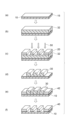
- FIG. 1 is a perspective view showing an example of a manufacturing process for a printed wiring board by a semi-additive method.
- the term “process” includes not only independent processes, but also processes that cannot be clearly distinguished from other processes, as long as the intended effect of the process is achieved.
- a numerical range indicated using “ ⁇ ” indicates a range that includes the numerical values before and after " ⁇ " as the minimum and maximum values, respectively.
- the upper or lower limit of a numerical range of a certain stage may be replaced with the upper or lower limit of a numerical range of another stage.
- the upper or lower limit of the numerical range may be replaced with a value shown in an example.
- the term “layer” includes a structure that is formed over the entire surface when observed in a plan view, as well as a structure that is formed on a part of the surface.
- “(Meth)acrylic acid” means at least one of "acrylic acid” and the corresponding "methacrylic acid”. The same applies to other similar expressions such as (meth)acrylate.
- the amount of each component in a composition when referring to the amount of each component in a composition, if the composition contains multiple substances corresponding to each component, it means the total amount of those multiple substances present in the composition, unless otherwise specified.
- room temperature refers to 25°C.
- solid content refers to the non-volatile content in a photosensitive resin composition excluding volatile substances (water, solvents, etc.). In other words, it refers to components other than substances (water, solvents, etc.) that do not volatilize during the drying process and remain, and includes liquid, starch syrup, and wax-like substances at around room temperature (25°C).
- (Poly)oxyethylene group means an oxyethylene group or a polyoxyethylene group in which two or more ethylene groups are linked by ether bonds.
- (Poly)oxypropylene group means an oxypropylene group or a polyoxypropylene group in which two or more propylene groups are linked by ether bonds.
- EO-modified means a compound having a (poly)oxyethylene group.
- PO-modified means a compound having a (poly)oxypropylene group.
- EO/PO-modified means a compound having both a (poly)oxyethylene group and a (poly)oxypropylene group.
- the photosensitive resin composition according to this embodiment contains (A) a binder polymer (hereinafter also referred to as (A) component), (B) a photopolymerizable compound having at least one ethylenically unsaturated bond (hereinafter also referred to as (B) component), and (C) a photopolymerization initiator (hereinafter also referred to as (C) component).
- the (C) photopolymerization initiator includes an oxime ester-based photopolymerization initiator.
- the content of the oxime ester-based photopolymerization initiator is 0.3 parts by mass or more relative to a total of 100 parts by mass of the (A) binder polymer and the (B) photopolymerizable compound.
- the photosensitive resin composition according to this embodiment contains 0.3 parts by mass or more of an oxime ester-based photopolymerization initiator as component (C) per 100 parts by mass of the total of components (A) and (B), and therefore in both the mask exposure method and the direct writing method, when a resist pattern is formed, it is possible to suppress the resulting resist line width from being wider or narrower than the design value, and it is possible to reduce the deviation of the resulting resist line width from the design value.
- the cured product according to this embodiment is a cured product of the photosensitive resin composition according to this embodiment.
- the cured product according to this embodiment may be a resist pattern.
- the photosensitive resin composition according to this embodiment may contain a (meth)acrylic resin, and the (A) component may have a structural unit derived from (meth)acrylic acid.
- the (A) component may have a structural unit derived from a polymerizable monomer other than (meth)acrylic acid.
- the (A) component has at least a structural unit derived from (meth)acrylic acid and a structural unit derived from benzyl (meth)acrylate or a benzyl (meth)acrylate derivative.
- the component (A) may have a structural unit derived from a hydroxyalkyl (meth)acrylate.
- the component (A) can be produced, for example, by radical polymerization of a polymerizable monomer.
- the above-mentioned polymerizable monomers other than (meth)acrylic acid include, for example, styrene; polymerizable styrene derivatives substituted at the ⁇ -position or aromatic ring, such as vinyl toluene and ⁇ -methyl styrene; alkyl (meth)acrylates; benzyl (meth)acrylate; benzyl (meth)acrylate derivatives; acrylamides such as diacetone acrylamide; acrylonitrile; esters of vinyl alcohol, such as vinyl-n-butyl ether; cycloalkyl (meth)acrylates; furfuryl (meth)acrylate; tetrahydrofurfuryl (meth)acrylate; isobornyl (meth)acrylate; adamantane (meth)acrylate.
- styrene polymerizable styrene derivatives substituted at the ⁇ -position or aromatic ring, such as vinyl tol
- ethyl dicyclopentanyl (meth)acrylate; dimethylaminoethyl (meth)acrylate; diethylaminoethyl (meth)acrylate; glycidyl (meth)acrylate; 2,2,2-trifluoroethyl (meth)acrylate; 2,2,3,3-tetrafluoropropyl (meth)acrylate; ⁇ -furyl (meth)acrylic acid; ⁇ -styryl (meth)acrylic acid; maleic acid; maleic anhydride; maleic acid monoesters such as monomethyl maleate, monoethyl maleate, and monoisopropyl maleate; fumaric acid; cinnamic acid; ⁇ -cyanocinnamic acid; itaconic acid; crotonic acid; and propiolic acid.
- Examples of benzyl (meth)acrylate derivatives include compounds in which the aromatic ring of a benzyl group is substituted with an alkoxy group having 1 to 6 carbon atoms (the number of carbon atoms; the same applies below), a halogen atom, and/or an alkyl group having 1 to 6 carbon atoms.
- Examples of benzyl (meth)acrylate derivatives include ethoxybenzyl (meth)acrylate, methoxybenzyl (meth)acrylate, chlorobenzyl (meth)acrylate, methylbenzyl (meth)acrylate, and ethylbenzyl (meth)acrylate.
- the (A) component may have at least one structural unit derived from styrene or a styrene derivative. By further improving the resolution, an even better resist shape can be obtained.
- the (A) component may have a structural unit derived from styrene and a structural unit derived from a styrene derivative.
- hydroxyalkyl (meth)acrylates examples include hydroxymethyl (meth)acrylate, hydroxyethyl (meth)acrylate, hydroxypropyl (meth)acrylate, hydroxybutyl (meth)acrylate, hydroxypentyl (meth)acrylate, and hydroxyhexyl (meth)acrylate.
- the hydroxyalkyl (meth)acrylate may have a branched structure.
- the (A) component may have at least one structural unit derived from an alkyl (meth)acrylate, from the viewpoint of improving the alkaline developability and the peeling properties.
- alkyl group of the alkyl (meth)acrylate include a methyl group, an ethyl group, a propyl group, a butyl group, a pentyl group, a hexyl group, a heptyl group, an octyl group, a nonyl group, a decyl group, a undecyl group, and a dodecyl group.
- each structural isomer can be used as the alkyl group.
- alkyl (meth)acrylate examples include methyl (meth)acrylate, ethyl (meth)acrylate, propyl (meth)acrylate, butyl (meth)acrylate, pentyl (meth)acrylate, hexyl (meth)acrylate, heptyl (meth)acrylate, octyl (meth)acrylate, 2-ethylhexyl (meth)acrylate, nonyl (meth)acrylate, decyl (meth)acrylate, undecyl (meth)acrylate, and dodecyl (meth)acrylate.
- the number of carbon atoms of the alkyl group may be 1 to 4, from the viewpoint of further improving the peeling properties.
- the alkyl (meth)acrylate can be used alone or in any combination of two or more types.
- the content of each structural unit constituting the (A) component is not particularly limited.
- the content of the structural unit derived from (meth)acrylic acid may be such that the acid value of the (A) component is in the following range.
- the acid value of the (A) component may be 100 mgKOH/g or more, 120 mgKOH/g or more, 140 mgKOH/g or more, or 150 mgKOH/g or more, from the viewpoint of suppressing an increase in the development time.
- the acid value of the (A) component may be 250 mgKOH/g or less, 240 mgKOH/g or less, or 230 mgKOH/g or less, from the viewpoint of further improving the developer resistance (e.g., adhesion) of the cured product of the photosensitive resin composition.
- the acid value of the (A) component may be 100 to 250 mgKOH/g, 120 to 240 mgKOH/g, 140 to 230 mgKOH/g, or 150 to 230 mgKOH/g.
- the amount of polymerizable monomer having a carboxy group may be adjusted to a small amount in order to improve developability.
- the content of the structural unit may be in the following ranges based on the total solid content (total mass) of component (A). From the viewpoint of improving the chemical resistance of the resin, the content may be 1 mass% or more, 15 mass% or more, or 20 mass% or more. From the viewpoint of suppressing an increase in the peeling time, the content may be 80 mass% or less, 50 mass% or less, or 40 mass% or less. From these viewpoints, the content may be 1 to 80 mass%, 15 to 50 mass%, or 20 to 40 mass%.
- the content of the structural unit may be in the following ranges based on the total amount (total mass) of solids in component (A). From the viewpoint of further improving resolution, the content may be 5 mass% or more, 10 mass% or more, or 20 mass% or more. From the viewpoint of suppressing the peeling pieces from becoming large and suppressing the peeling time from becoming long, the content may be 65 mass% or less, 55 mass% or less, or 50 mass% or less. From these viewpoints, the content may be 5 to 65 mass%, 10 to 55 mass%, or 20 to 50 mass%.
- the content of the structural unit may be in the following ranges based on the total solid content (total mass) of component (A).
- the content may be 1 mass% or more, 2 mass% or more, or 3 mass% or more, from the viewpoint of preventing peeling pieces from becoming large and preventing the peeling time from becoming long.
- the content may be 80 mass% or less, 60 mass% or less, or 50 mass% or less, from the viewpoint of further improving resolution and adhesion. From these viewpoints, the content may be 1 to 80 mass%, 2 to 60 mass%, or 3 to 50 mass%.
- the weight average molecular weight (Mw) of the (A) component may be 10,000 or more, 20,000 or more, or 25,000 or more, from the viewpoint that the developer resistance (e.g., adhesion) of the cured product of the photosensitive resin composition tends to be even better.
- the weight average molecular weight (Mw) of the (A) component may be 100,000 or less, 80,000 or less, or 60,000 or less, from the viewpoint that the development time tends to be excellent. From these viewpoints, the weight average molecular weight (Mw) of the (A) component may be 10,000 to 100,000, 20,000 to 80,000, or 25,000 to 60,000.
- the weight average molecular weight of the (A) component is measured by gel permeation chromatography (GPC) (converted by a calibration curve using standard polystyrene). For compounds with low molecular weights, if it is difficult to measure the weight average molecular weight using the above-mentioned method, the molecular weight may be measured by another method and the average calculated.
- GPC gel permeation chromatography
- the degree of dispersion (Mw/Mn) of component (A) is not particularly limited, but may be 1.0 to 3.0, or 1.5 to 2.5. If the degree of dispersion is 3.0 or less, adhesion and resolution are further improved.
- component (A) may have a characteristic group (such as a nitro group) in its molecule that is sensitive to light having a wavelength in the range of 350 to 440 nm.
- a characteristic group such as a nitro group
- one type of binder polymer may be used alone as component (A), or two or more types of binder polymers may be used in any combination.
- component (A) include two or more types of binder polymers made of different copolymerization components (binder polymers containing different monomer units as copolymerization components), two or more types of binder polymers with different weight average molecular weights, and two or more types of binder polymers with different dispersities.
- component (A) a polymer having a multimodal molecular weight distribution as described in JP-A-11-327137 (Patent Document 3) can also be used.
- the content of component (A) may be within the following ranges based on the total solid content (total mass) of the photosensitive resin composition. From the viewpoint of a tendency for excellent film formability, the content of component (A) may be 20 mass% or more, 30 mass% or more, 40 mass% or more, or 50 mass% or more. From the viewpoint of a tendency for even better sensitivity and resolution, the content of component (A) may be 90 mass% or less, 80 mass% or less, 65 mass% or less, or 60 mass% or less. From these viewpoints, the content of component (A) may be 20 to 90 mass%, 30 to 80 mass%, 40 to 65 mass%, or 50 to 60 mass%.
- the content of component (A) may be within the following ranges relative to 100 parts by mass of the total amount of components (A) and (B). From the viewpoint of further improving film formability, the content of component (A) may be 30 parts by mass or more, 35 parts by mass or more, 40 parts by mass or more, or 50 parts by mass or more. From the viewpoint of further improving sensitivity and resolution, the content of component (A) may be 70 parts by mass or less, 65 parts by mass or less, or 60 parts by mass or less. From these viewpoints, the content of component (A) may be 30 to 70 parts by mass, 35 to 65 parts by mass, 40 to 60 parts by mass, or 50 to 60 parts by mass.
- the component (B) component is a compound having at least one ethylenically unsaturated bond.
- the component (B) may be used alone or in any combination of two or more kinds.
- the component (B) is From the viewpoint of further improving the alkali developability, the resolution, and the peelability after curing, at least one bisphenol A type (meth)acrylate compound may be contained.
- bisphenol A type (meth)acrylate compounds examples include 2,2-bis(4-((meth)acryloxypolyethoxy)phenyl)propane, 2,2-bis(4-((meth)acryloxypolypropoxy)phenyl)propane, 2,2-bis(4-((meth)acryloxypolybutoxy)phenyl)propane, 2,2-bis(4-((meth)acryloxypolyethoxypolypropoxy)phenyl)propane, and the like.
- component (B) may contain 2,2-bis(4-((meth)acryloxypolyethoxy)phenyl)propane from the viewpoint of further improving resolution and peeling properties.
- the bisphenol A type (meth)acrylate compounds may be used alone or in any combination of two or more.
- BPE-200 Japanese Patent Application Laida Chemical Co., Ltd.
- BPE-500 Japanese Patent Application Laida Chemical Co., Ltd.
- FA-321M trade name, manufactured by Resonac Corporation
- the content of the bisphenol A type (meth)acrylate compound may be in the following range based on the total amount (total mass) of the solid content of component (B) from the viewpoint of further improving the resolution of the resist pattern.
- the content may be 20 mass% or more, 40 mass% or more, 60 mass% or more, or 70 mass% or more.
- the content may be 100 mass% or less, or 95 mass% or less. From these viewpoints, the content may be 20 to 100 mass%, 40 to 100 mass%, 60 to 100 mass%, or 70 to 100 mass%, or may be 20 to 95 mass%, 40 to 95 mass%, 60 to 95 mass%, or 70 to 95 mass%.
- component (B) may contain a compound obtained by reacting a polyhydric alcohol with an ⁇ , ⁇ -unsaturated carboxylic acid.
- compounds obtained by reacting a polyhydric alcohol with an ⁇ , ⁇ -unsaturated carboxylic acid include polyethylene glycol di(meth)acrylate having 2 to 14 ethylene groups; polypropylene glycol di(meth)acrylate having 2 to 14 propylene groups; alkylene glycol di(meth)acrylate having both a (poly)oxyethylene group and a (poly)oxypropylene group; trimethylolpropane di(meth)acrylate; trimethylolpropane tri(meth)acrylate; EO-modified trimethylolpropane tri(meth)acrylate; PO-modified trimethylolpropane tri(meth)acrylate; EO/PO-modified trimethylolpropane tri(meth)acrylate; tetramethylo
- two or more types selected from the group of compounds obtained by reacting the above polyhydric alcohol with an ⁇ , ⁇ -unsaturated carboxylic acid may be used in combination. Combining two or more types further improves the resolution.
- the content (total amount) of the above compound obtained by reacting a polyhydric alcohol with an ⁇ , ⁇ -unsaturated carboxylic acid may be in the following range based on the total amount (total mass) of solids in component (B). From the viewpoint of improving flexibility, the content may be 5 mass% or more. From the viewpoint of further improving resolution, the content may be 20 mass% or less or 15 mass% or less. From these viewpoints, the content may be 5 to 20 mass% or 5 to 15 mass%.
- the photosensitive resin composition in this embodiment can further contain, as component (B), a polymerizable compound other than the above-mentioned bisphenol A type (meth)acrylate compound and the above-mentioned compound obtained by reacting a polyhydric alcohol with an ⁇ , ⁇ -unsaturated carboxylic acid.
- component (B) a polymerizable compound other than the above-mentioned bisphenol A type (meth)acrylate compound and the above-mentioned compound obtained by reacting a polyhydric alcohol with an ⁇ , ⁇ -unsaturated carboxylic acid.
- polymerizable compounds include nonylphenoxy polyethyleneoxy (meth)acrylate, phthalic acid compounds, alkyl (meth)acrylate, and photopolymerizable compounds having at least one cationic polymerizable cyclic ether group in the molecule (such as oxetane compounds).
- at least one selected from the group consisting of nonylphenoxy polyethyleneoxy (meth)acrylate and phthalic acid compounds is preferred from the viewpoint of achieving a well-balanced improvement in resolution, adhesion, resist shape, and peeling properties after curing.
- the nonylphenoxy polyethyleneoxy (meth)acrylates include, for example, nonylphenoxy triethyleneoxy (meth)acrylate, nonylphenoxy tetraethyleneoxy (meth)acrylate, nonylphenoxy pentaethyleneoxy (meth)acrylate, nonylphenoxy hexaethyleneoxy (meth)acrylate, nonylphenoxy heptaethyleneoxy (meth)acrylate, nonylphenoxy octaethyleneoxy (meth)acrylate, nonylphenoxy nonaethyleneoxy (meth)acrylate, nonylphenoxy decaethyleneoxy (meth)acrylate, and nonylphenoxy undecaethyleneoxy (meth)acrylate.
- the nonylphenoxy polyethyleneoxy (meth)acrylates can be used alone or in any combination of two or more.
- phthalic acid compounds include ⁇ -chloro- ⁇ -hydroxypropyl- ⁇ '-(meth)acryloyloxyethyl-o-phthalate, ⁇ -hydroxyethyl- ⁇ '-(meth)acryloyloxyethyl-o-phthalate, and ⁇ -hydroxypropyl- ⁇ '-(meth)acryloyloxyethyl-o-phthalate.
- ⁇ -chloro- ⁇ -hydroxypropyl- ⁇ '-(meth)acryloyloxyethyl-o-phthalate is preferred as the phthalic acid compound.
- ⁇ -chloro- ⁇ -hydroxypropyl- ⁇ '-methacryloyloxyethyl-o-phthalate is commercially available as FA-MECH (trade name, manufactured by Resonac Corporation). Phthalic acid compounds can be used alone or in any combination of two or more.
- the content of the photopolymerizable compound may be 1 to 30 mass%, 3 to 25 mass%, or 5 to 20 mass% based on the total solid content (total mass) of component (B) from the viewpoint of improving the resolution, adhesion, resist shape, and peeling properties after curing in a well-balanced manner.
- the content of the (B) component may be within the following ranges based on the total solid content (total mass) of the photosensitive resin composition. From the viewpoint of a tendency for the sensitivity and resolution to be even more excellent, the content of the (B) component may be 3 mass% or more, 10 mass% or more, 25 mass% or more, 30 mass% or more, or 40 mass% or more. From the viewpoint of a tendency for the film formability to be excellent, the content of the (B) component may be 70 mass% or less, 60 mass% or less, or 50 mass% or less. From these viewpoints, the content of the (B) component may be 3 to 70 mass%, 10 to 60 mass%, 25 to 50 mass%, 30 to 50 mass%, or 40 to 50 mass%.
- the content of the (B) component may be in the following ranges relative to 100 parts by mass of the total amount of the (A) component and the (B) component. From the viewpoint of further improving the sensitivity and resolution, the content of the (B) component may be 5 parts by mass or more, 10 parts by mass or more, 15 parts by mass or more, 20 parts by mass or more, 30 parts by mass or more, or 40 parts by mass or more. From the viewpoint of further improving the formability of the film, the content of the (B) component may be 70 parts by mass or less, 65 parts by mass or less, 60 parts by mass or less, 50 parts by mass or less, or 45 parts by mass or less. From these viewpoints, the content of the (B) component may be 5 to 70 parts by mass, 10 to 70 parts by mass, 15 to 65 parts by mass, 20 to 60 parts by mass, 30 to 50 parts by mass, or 40 to 45 parts by mass.
- Component (C): Photopolymerization initiator The photosensitive resin composition according to the present embodiment contains an oxime ester-based photopolymerization initiator as component (C), which can reduce deviation of the resulting resist line width from the designed value when a resist pattern is formed in either the mask exposure method or the direct writing method.
- the oxime ester photopolymerization initiator is not particularly limited as long as it is a photopolymerization initiator having an oxime ester group, but is preferably a compound having at least one of a carbazole structure, a phenyl sulfide structure, and a fluorene structure. This makes it possible to further reduce the deviation of the resist line width obtained when a resist pattern is formed from the designed value in both the mask exposure method and the direct writing method.
- the oxime ester photopolymerization initiator can be used alone or in any combination of two or more types.
- oxime ester photopolymerization initiators having a carbazole structure examples include 1-propanone, 3-cyclopentyl-1-[9-ethyl-6-(2-methylbenzoyl)-9H-carbazol-3-yl]-, 1-(o-acetyloxime) (product name "TR-PBG-304", manufactured by Changzhou New Strong Electronic Materials Co., Ltd.), 1-propanone, 3-cyclopentyl-1-[2-(2-pyrimidinylthio)-9H-carbazol-3-yl]-, 1-(o-acetyloxime) (product name "TR-PBG-314", manufactured by Changzhou New Strong Electronic Materials Co., Ltd.), 2-(acetoxyimino)-1-(6-(2-(acetoxyimino)-3-cyclohexylpropionyl)-9-ethylcarbazol-3-yl) n-octan-1-one, and the like.
- Commercially available products include TR-PBG-304, TR-
- An example of an oxime ester photopolymerization initiator having a phenyl sulfide structure is 1-[4-(phenylthio)phenyl]-3-cyclopentylpropane-1,2-dione-2-(o-benzoyloxime) (trade name "TR-PBG-305", manufactured by Changzhou Strong Electronic New Materials Co., Ltd.).
- TR-PBG-305 manufactured by Changzhou Strong Electronic New Materials Co., Ltd.
- Commercially available products include TR-PBG-305 and TR-PBG-3057 (both manufactured by Changzhou Strong Electronic New Materials Co., Ltd.).
- An example of an oxime ester photopolymerization initiator having a fluorene structure is (Z)-[3-cyclohexyl-1-(9,9-dibutyl-7-nitrofluoren-2-yl)propylidene]amino)acetate.
- Commercially available products include TR-PBG-358 (manufactured by Changzhou Strong Electronic New Materials Co., Ltd.).
- the oxime ester photopolymerization initiator may be a compound that does not have any of the carbazole structure, the phenyl sulfide structure, and the fluorene structure.
- Examples of such oxime ester photopolymerization initiators include 1-phenyl-1,2-propane oxime dione 2-(o-benzoyl oxime).
- the content of the oxime ester photopolymerization initiator is 0.3 parts by mass or more per 100 parts by mass of the total of the (A) component and the (B) component. This makes it possible to reduce the deviation of the resist line width from the design value when forming a resist pattern in both the mask exposure method and the direct writing method. From the viewpoint of further enhancing the above effect, the content of the oxime ester photopolymerization initiator may be 0.35 parts by mass or more, or 0.4 parts by mass or more per 100 parts by mass of the total of the (A) component and the (B) component.
- the content of the oxime ester photopolymerization initiator may be 3.0 parts by mass or less, 2.5 parts by mass or less, or 2.0 parts by mass or less per 100 parts by mass of the total of the (A) component and the (B) component. From these viewpoints, the content of the oxime ester photopolymerization initiator may be 0.3 to 3.0 parts by mass, 0.35 to 2.5 parts by mass, or 0.4 to 2.0 parts by mass per 100 parts by mass of the total of the (A) component and the (B) component.
- the content of the oxime ester photopolymerization initiator may be in the following ranges based on the total mass of component (C) from the viewpoint of obtaining appropriate sensitivity.
- the content of the oxime ester photopolymerization initiator may be 50% by mass or more, 60% by mass or more, 65% by mass or more, 70% by mass or more, or 75% by mass or more.
- the content of the oxime ester photopolymerization initiator may be 100% by mass.
- the (C) photopolymerization initiator may consist only of the oxime ester photopolymerization initiator. From these viewpoints, the content may be 50 to 100% by mass, 60 to 100% by mass, 65 to 100% by mass, 70 to 100% by mass, or 75 to 100% by mass.
- the photosensitive resin composition according to this embodiment may further contain a photopolymerization initiator other than the oxime ester photopolymerization initiator.
- a photopolymerization initiator other than the oxime ester photopolymerization initiator.
- other photopolymerization initiators include hexaarylbiimidazole derivatives.
- the photopolymerization initiator is preferably at least one type of 2,4,5-triarylimidazole dimer.
- the structure of the 2,4,5-triarylimidazole dimer may be symmetric or asymmetric.
- 2,4,5-triarylimidazole dimer examples include 2-(o-chlorophenyl)-4,5-diphenylimidazole dimer (also known as 2,2'-bis(o-chlorophenyl)-4,4',5,5'-tetraphenyl-1,2'-biimidazole), 2-(o-chlorophenyl)-4,5-bis-(m-methoxyphenyl)imidazole dimer, and 2-(p-methoxyphenyl)-4,5-diphenylimidazole dimer. Among these, 2-(o-chlorophenyl)-4,5-diphenylimidazole dimer is preferred.
- photopolymerization initiators include aromatic ketones such as benzophenone, 2-benzyl-2-dimethylamino-1-(4-morpholinophenyl)-butanone-1,2-(dimethylamino)-2-[(4-methylphenyl)methyl]-1-[4-(4-morpholinyl)phenyl]-1-butanone, 4-(2-hydroxyethoxy)phenyl-2-(hydroxy-2-propyl)ketone, and 2-methyl-1-[4-(methylthio)phenyl]-2-morpholino-propanone-1; alkyl ketones such as benzophenone, 2-benzyl-2-dimethylamino-1-(4-morpholinophenyl)butanone-1,2-dimethylamino-2-[(4-methylphenyl)methyl]-1-[4-(4-morpholinyl)phenyl]-1-butanone; These include quinones such as tribenzone; benzoin ether compounds such as benzoin alkyl
- the content of the photopolymerization initiator may be 0.01 to 10 parts by mass, 0.01 to 8 parts by mass, or 0.01 to 5 parts by mass per 100 parts by mass of the total of the (A) component and the (B) component.
- the content of the (C) component may be in the following ranges based on the total amount of solids (total mass) of the photosensitive resin composition.
- the content of the (C) component may be 0.1 mass% or more, 0.2 mass% or more, 0.3 mass% or more, or 0.35 mass% or more.
- the content of the (C) component may be 20 mass% or less, 10 mass% or less, 3 mass% or less, 1 mass% or less, 0.5 mass% or less, or 0.4 mass% or less. From these viewpoints, the content of the (C) component may be 0.1 to 20 mass%, 0.1 to 10 mass%, or 0.1 to 3 mass%.
- the photosensitive resin composition according to this embodiment may further contain a hydrogen donor capable of providing hydrogen during the reaction of the exposed area, thereby further improving the sensitivity of the photosensitive resin composition.
- Examples of the (D) component include bis[4-(dimethylamino)phenyl]methane, bis[4-(diethylamino)phenyl]methane, leuco crystal violet, and N-phenylglycine.
- the (D) component can be used alone or in any combination of two or more types.
- the content of the (D) component may be in the following ranges relative to 100 parts by mass of the total of the (A) and (B) components. From the viewpoint of further improving the sensitivity, the content of the (D) component may be 0.01 parts by mass or more, 0.05 parts by mass or more, 0.1 parts by mass or more, 0.3 parts by mass or more, 0.5 parts by mass or more, or 0.6 parts by mass or more. From the viewpoint of suppressing the precipitation of the excess (D) component as foreign matter after film formation, the content of the (D) component may be 10 parts by mass or less, 5 parts by mass or less, 2 parts by mass or less, or 1 part by mass or less. From these viewpoints, the content of the (D) component may be 0.01 to 10 parts by mass, 0.05 to 5 parts by mass, or 0.1 to 2 parts by mass.
- the photosensitive resin composition according to this embodiment may further contain a sensitizing dye. This further improves the sensitivity of the photosensitive resin composition.
- sensitizing dyes include dialkylaminobenzophenones, pyrazolines, anthracenes, coumarins, xanthones, oxazoles, benzoxazoles, thiazoles, benzothiazoles, triazoles, stilbenes, triazines, thiophenes, naphthalimides, and triarylamines.
- the sensitizing dyes may be used alone or in any combination of two or more.
- the sensitizing dye may contain at least one selected from the group consisting of pyrazolines, anthracenes, coumarins, and triarylamines, from the viewpoint of further improving sensitivity and adhesion, and may contain at least one selected from the group consisting of pyrazolines, anthracenes, and triarylamines.
- the content of the sensitizing dye may be 0.01 to 10 parts by mass, 0.05 to 5 parts by mass, or 0.1 to 3 parts by mass, relative to 100 parts by mass of the total amount of the (A) component and the (B) component.
- the content of the sensitizing dye is 0.01 parts by mass or more, the sensitivity and resolution are further improved.
- the content of the sensitizing dye is 10 parts by mass or less, the resist shape is further prevented from becoming an inverted trapezoid, and the adhesion is further improved.
- the photosensitive resin composition according to the present embodiment may contain other components as necessary.
- the other components include dyes (such as malachite green), tribromophenyl sulfone, photocoloring agents, thermal color-developing inhibitors, plasticizers (such as p-toluenesulfonamide), pigments, fillers, defoamers, flame retardants, stabilizers, adhesion agents, leveling agents, peeling promoters, antioxidants, fragrances, imaging agents, and thermal crosslinking agents. These may be used alone or in any combination of two or more.
- the content of each of these components is preferably about 0.01 to 20 parts by mass per 100 parts by mass of the total amount of components (A) and (B).
- the photosensitive resin composition according to this embodiment may contain at least one organic solvent to adjust the viscosity, if necessary.
- organic solvent any commonly used organic solvent may be used without any particular restrictions. Examples of organic solvents include methanol, ethanol, acetone, methyl ethyl ketone, methyl cellosolve, ethyl cellosolve, toluene, N,N-dimethylformamide, propylene glycol monomethyl ether, and mixed solvents thereof.
- the photosensitive resin composition according to this embodiment can be used as a solution (hereinafter referred to as the "coating liquid") with a solid content of about 30 to 60% by mass by dissolving, for example, at least the (A), (B), and (C) components in the organic solvent.
- the coating liquid can be used, for example, to form a photosensitive resin layer as follows.
- the coating liquid is applied to the surface of a support (support film, metal plate, etc.) described below, and then dried to form a photosensitive resin layer derived from the photosensitive resin composition on the support.
- Metal plates include copper, copper-based alloys, nickel, chromium, iron, iron-based alloys (stainless steel, etc.), and preferably copper, copper-based alloys, iron-based alloys, etc.
- the thickness of the photosensitive resin layer varies depending on the application, but may be approximately 1 to 100 ⁇ m after drying.
- the photosensitive resin composition according to this embodiment can be suitably used, for example, in the method of forming a resist pattern described below. In particular, it is suitable for application to a method of forming a conductor pattern (circuit) by plating.
- the photosensitive element according to the present embodiment includes a support and a photosensitive resin layer disposed on the support.
- the photosensitive resin layer includes the photosensitive resin composition according to the present embodiment or a cured product thereof.
- the photosensitive resin layer is formed using the photosensitive resin composition according to the present embodiment, and the photosensitive resin composition may be in an uncured state (coating film).
- the photosensitive element may include other layers such as a protective layer, if necessary.
- the surface (surface) of the photosensitive resin layer opposite to the surface facing the support may be covered with a protective layer (protective film, etc.).
- FIG. 1 shows one embodiment of a photosensitive element.
- a support 2, a photosensitive resin layer 3, and a protective layer 4 are laminated in this order.
- the photosensitive element 1 can be obtained, for example, as follows. A coating liquid that is a photosensitive resin composition is applied onto the support 2 to form a coating layer, and the coating layer is then dried to form the photosensitive resin layer 3. Next, the surface of the photosensitive resin layer 3 opposite the support 2 is covered with a protective layer 4, thereby obtaining a photosensitive element 1 that includes the support 2, the photosensitive resin layer 3 formed on the support 2, and the protective layer 4 laminated on the photosensitive resin layer 3.
- the photosensitive element 1 does not necessarily have to include the protective layer 4.
- the support may be a polymer film having heat resistance and solvent resistance, such as a polyethylene terephthalate film, a polyethylene film, a polypropylene film, or a polyester film.
- the thickness of the support may be 1 to 100 ⁇ m, 5 to 50 ⁇ m, or 5 to 30 ⁇ m.
- the thickness of the support is 1 ⁇ m or more, it is easy to prevent the support from breaking when peeling it off.
- the thickness of the support is 100 ⁇ m or less, it is easy to prevent a decrease in resolution when exposure is performed through the support.
- the protective layer (protective film, etc.) preferably has a smaller adhesive strength to the photosensitive resin layer than the adhesive strength of the support to the photosensitive resin layer, and is preferably a film with low fisheyes.
- fisheyes refers to foreign matter, undissolved matter, oxidized deterioration products, etc. of the material that constitutes the protective film that are introduced into the film when the film is manufactured by thermally melting the material and kneading, extrusion, biaxial stretching, casting, etc.
- low fisheyes means that the film has few of the above foreign matter, etc.
- the protective layer may be a polymer film having heat resistance and solvent resistance, such as a polyethylene terephthalate film, a polyethylene film, a polypropylene film, or a polyester film.
- a polymer film having heat resistance and solvent resistance such as a polyethylene terephthalate film, a polyethylene film, a polypropylene film, or a polyester film.
- Commercially available polymer films include polypropylene films manufactured by Oji Paper Co., Ltd. (e.g., Alphan MA-410 and E-200C) and Shin-Etsu Film Co., Ltd.; and polyethylene terephthalate films such as PS-25 (e.g., PS series) manufactured by Teijin Limited.
- the protective layer may be the same type of material as the support, or a different type of material.
- the thickness of the protective layer may be 1 to 100 ⁇ m, 5 to 50 ⁇ m, 5 to 30 ⁇ m, or 15 to 30 ⁇ m.
- the thickness of the protective layer is 1 ⁇ m or more, it is possible to prevent the protective layer from being torn when the photosensitive resin layer and the support are laminated onto the base material (substrate, etc.) while peeling off the protective layer.
- the thickness of the protective layer is 100 ⁇ m or less, productivity is improved.
- the photosensitive element according to this embodiment can be manufactured, for example, as follows.
- the photosensitive element can be manufactured by a manufacturing method including the steps of dissolving at least the (A), (B), and (C) components in an organic solvent to prepare a coating solution with a solid content of about 30 to 60% by mass, applying the coating solution onto a support to form a coating layer, and drying the coating layer to form a photosensitive resin layer.
- the coating solution can be applied onto the support by known methods such as roll coating, comma coating, gravure coating, air knife coating, die coating, and bar coating.
- drying method of the coating layer There are no particular limitations on the drying method of the coating layer, as long as at least a portion of the organic solvent can be removed from the coating layer. For example, drying may be performed at 70 to 150°C for about 5 to 30 minutes. The amount of organic solvent remaining in the photosensitive resin layer after drying may be 2 mass% or less, from the viewpoint of preventing diffusion of the organic solvent in subsequent steps.
- the thickness of the photosensitive resin layer in the photosensitive element according to this embodiment can be appropriately selected depending on the application, but may be 1 to 100 ⁇ m, 1 to 50 ⁇ m, or 5 to 40 ⁇ m after drying. When the thickness of the photosensitive resin layer is 1 ⁇ m or more, industrial coating becomes easier and productivity improves. When the thickness of the photosensitive resin layer is 100 ⁇ m or less, adhesion and resolution are further improved.
- the photosensitive element according to this embodiment may further include known intermediate layers, such as a cushion layer, an adhesive layer, a light absorbing layer, and a gas barrier layer, as necessary.
- the form of the photosensitive element according to this embodiment is not particularly limited.
- the photosensitive element may be, for example, in the form of a sheet, or may be wound in the form of a roll around a core.
- the photosensitive element according to this embodiment can be suitably used, for example, in the resist pattern forming method described below. In particular, it is suitable for application to a method of forming a conductor pattern (circuit) by plating.
- the method for forming a resist pattern according to this embodiment includes: (i) a step of forming a photosensitive resin layer on a base material (substrate or the like) using the photosensitive resin composition or the photosensitive element (photosensitive resin layer forming step); (ii) a step of irradiating at least a part of the photosensitive resin layer with active light rays to cure the photosensitive resin layer (exposure step); and (iii) a step of removing the uncured part of the photosensitive resin layer from the base material to form a resist pattern (development step), and may include other steps as necessary.
- the resist pattern may also be called a relief pattern.
- the method for forming a resist pattern according to this embodiment may also be called a method for producing a base material with a resist pattern.
- a photosensitive resin layer is formed on a base material (substrate or the like) using the photosensitive resin composition or the photosensitive element.
- the base material is not particularly limited, but may be:
- a substrate having a conductor layer can be used.
- the substrate having a conductor layer can be a circuit board having an insulating layer and a conductor layer formed on the insulating layer, or a die pad (for a lead frame).
- Substrates, such as alloy substrates, can be used.
- a method for forming a photosensitive resin layer on a substrate includes, for example, removing a protective layer from the photosensitive element, and then heating and pressing the photosensitive resin layer of the photosensitive element onto the substrate. This results in a laminate consisting of the substrate, photosensitive resin layer, and support, which are laminated in this order.
- the photosensitive resin layer may be formed by applying and drying the photosensitive resin composition.
- This photosensitive resin layer forming step is preferably carried out under reduced pressure from the viewpoint of further improving adhesion and followability.
- the photosensitive resin layer and/or the base material may be heated at a temperature of 70 to 130 ° C. during pressure bonding. Pressure bonding may be performed at a pressure of about 0.1 to 1.0 MPa (about 1 to 10 kgf / cm 2 ). These conditions can be appropriately selected as needed. Note that if the photosensitive resin layer is heated to 70 to 130 ° C., it is not necessary to preheat the base material in advance, but in order to further improve adhesion and followability, the base material can also be preheated.
- Exposure Step In the exposure step, at least a part of a photosensitive resin layer formed on a base material (substrate or the like) is irradiated with active light rays, whereby the part irradiated with the active light rays is cured and a latent image is formed.
- actinic rays can be irradiated through the support. If the support is light-shielding, actinic rays can be irradiated onto the photosensitive resin layer after removing the support.
- a method of irradiating an image-wise pattern of active light rays using a direct imaging exposure method such as LDI (Laser Direct Imaging) exposure method or DLP (Digital Light Processing) exposure method may be used, or a method of irradiating an image-wise pattern of active light rays through a negative or positive mask pattern called artwork (mask exposure method) may be used, or these methods may be used in combination.
- a direct imaging exposure method such as LDI (Laser Direct Imaging) exposure method or DLP (Digital Light Processing) exposure method
- a method of irradiating an image-wise pattern of active light rays through a negative or positive mask pattern called artwork (mask exposure method) may be used, or these methods may be used in combination.
- a known light source can be used as the light source for the actinic rays.
- light sources that effectively emit ultraviolet or visible light such as carbon arc lamps, mercury vapor arc lamps, high-pressure mercury lamps, xenon lamps, gas lasers (argon lasers, etc.), solid-state lasers (YAG lasers, etc.), and semiconductor lasers, can be used.
- Examples of dominant wavelengths of actinic rays include 355 nm and 405 nm. The dominant wavelength refers to the set wavelength of the actinic rays, and for example, light with a dominant wavelength of 355 nm can include light with wavelengths of 352 to 358 nm.
- ((iii) Development process) In the development step, the uncured portion of the photosensitive resin layer is removed from the base material (substrate, etc.), and a resist pattern made of a cured product of the photosensitive resin layer is formed on the base material. When a support is present on the photosensitive resin layer, the support is removed, and then the unexposed areas other than the exposed areas are removed (developed). Although development and dry development are included, wet development is widely used.
- development can be performed by a known development method using a developer that is compatible with the photosensitive resin composition.
- Development methods include the dipping method, paddle method, spray method, brushing, slapping, scrubbing, and rocking immersion, and from the viewpoint of further improving resolution, the high-pressure spray method is most suitable. Development can be performed by combining two or more of these methods.
- the composition of the developer can be appropriately selected depending on the composition of the photosensitive resin composition.
- Examples of the developer include an alkaline aqueous solution and an organic solvent developer.
- alkaline aqueous solution When used as a developer, an alkaline aqueous solution is safe, stable, and easy to handle.
- bases for alkaline aqueous solutions include alkali hydroxides such as lithium, sodium, or potassium hydroxide; alkali carbonates such as lithium, sodium, potassium, or ammonium carbonates or bicarbonates; alkali metal phosphates such as potassium phosphate and sodium phosphate; alkali metal pyrophosphates such as sodium pyrophosphate and potassium pyrophosphate; borax; sodium metasilicate; tetramethylammonium hydroxide; ethanolamine; ethylenediamine; diethylenetriamine; 2-amino-2-hydroxymethyl-1,3-propanediol; 1,3-diamino-2-propanol; morpholine, etc.
- alkaline aqueous solution a dilute solution of 0.1 to 5 mass% sodium carbonate, a dilute solution of 0.1 to 5 mass% potassium carbonate, a dilute solution of 0.1 to 5 mass% sodium hydroxide, a dilute solution of 0.1 to 5 mass% sodium tetraborate, etc. are preferred.
- the pH of the alkaline aqueous solution is preferably 9 to 11.
- the temperature of the alkaline aqueous solution is adjusted according to the alkaline developability of the photosensitive resin layer.
- a surfactant, an antifoaming agent, a small amount of an organic solvent to promote development, etc. may be mixed into the alkaline aqueous solution.
- Organic solvents include acetone, ethyl acetate, alkoxyethanols having an alkoxy group with 1 to 4 carbon atoms, ethyl alcohol, isopropyl alcohol, butyl alcohol, diethylene glycol monomethyl ether, diethylene glycol monoethyl ether, and diethylene glycol monobutyl ether.
- the organic solvents may be used alone or in any combination of two or more.
- the content of the organic solvent in the aqueous developer is usually preferably 2 to 90% by mass, and the temperature can be adjusted according to the alkaline developability.
- Organic solvent developers include organic solvents such as 1,1,1-trichloroethane, N-methylpyrrolidone, N,N-dimethylformamide, cyclohexanone, methyl isobutyl ketone, and ⁇ -butyrolactone. To prevent ignition, it is preferable to add water to the organic solvent in the range of 1 to 20% by mass.
- the resist pattern after removing the unexposed portions in the development step, the resist pattern may be further hardened by heating at about 60 to 250° C. or exposing to about 0.2 to 10 J/cm 2 , if necessary.
- the method for producing a printed wiring board according to this embodiment includes a step of forming a resist pattern on a base material (such as a substrate) by the above-mentioned method for forming a resist pattern, and a step of forming a conductor pattern by subjecting the base material (such as a substrate) and a member having the resist pattern (base material on which a resist pattern is formed, base material with a resist pattern) to a plating process or an etching process.
- the method for producing a printed wiring board according to this embodiment may also include other steps, such as a step of removing the resist pattern, as necessary.
- a resist pattern formed on a base material can be used as a mask to perform plating or etching on the base material (for example, a conductor layer provided on the base material).
- the plating method in the method for manufacturing a printed wiring board may be either or both of electrolytic plating and electroless plating, and electroless plating is preferably used.
- electroless plating include copper plating such as copper sulfate plating and copper pyrophosphate plating; solder plating such as high-throw solder plating; Watts bath (nickel sulfate-nickel chloride) plating; nickel plating such as nickel sulfamate; and gold plating.
- the resist pattern can be peeled off using an aqueous solution that is more strongly alkaline than the aqueous solution used in the development step.
- an aqueous solution examples include a 1 to 10% by mass sodium hydroxide aqueous solution and a 1 to 10% by mass potassium hydroxide aqueous solution.
- Methods for this include an immersion method and a spray method, which may be used alone or in combination.
- the etching method can be appropriately selected depending on the conductor layer (metal layer) to be removed.
- etching solutions include cupric chloride solution, ferric chloride solution, alkaline etching solution, and hydrogen peroxide etching solution. Of these, it is preferable to use ferric chloride solution because of its good etch factor.
- the printed wiring board manufactured by the method for manufacturing a printed wiring board according to this embodiment may be a multilayer printed wiring board and may have small diameter through holes.
- the printed wiring board according to this embodiment can be manufactured by a manufacturing method including a process of forming a conductor pattern by performing an etching process or an etching process on a substrate on which a resist pattern has been formed by the resist pattern forming method according to this embodiment.
- a manufacturing method for a printed wiring board using the semi-additive method will be described below with reference to FIG. 2.
- a substrate (substrate for forming a circuit) is prepared in which a conductor layer 10 is formed on an insulating layer 15.
- the conductor layer 10 is, for example, a metallic copper layer.
- a photosensitive resin layer 32 is formed on the conductor layer 10 of the substrate by the photosensitive resin layer forming process.
- a mask 20 is placed on the photosensitive resin layer 32, and active light rays 50 are irradiated to expose the area other than the area where the mask 20 is placed, thereby forming a photocured portion.
- the area other than the photocured portion formed by the exposure process is removed from the substrate by a development process, thereby forming a resist pattern 30, which is a photocured portion, on the substrate.
- a plating layer 42 is formed on the conductor layer 10 by a plating process using the resist pattern 30, which is a photocured portion, as a mask.
- the photocured resist pattern 30 is peeled off with a strong alkaline aqueous solution, and then a flash etching process is performed to remove a part of the plating layer 42 and the conductor layer 10 that was masked by the resist pattern 30, forming the conductor pattern 40.
- the conductor layer 10 and the plating layer 42 may be made of the same material or different materials. When the conductor layer 10 and the plating layer 42 are made of the same material, the conductor layer 10 and the plating layer 42 may be integrated. Note that, although FIG. 2 describes a method of forming the resist pattern 30 using a mask 20, the resist pattern 30 may be formed by a direct writing exposure method without using a mask 20.
- A-1 A solution of a copolymer of methacrylic acid/styrene/benzyl methacrylate/2-hydroxyethyl methacrylate (mass ratio: 27/50/20/3, Mw: 35000, acid value: 176.1 mg KOH/g, Tg: 106.8° C.) in propylene glycol monomethyl ether/toluene (mass ratio 3/4) (solid content: 49.6% by mass)
- A-2 A solution of a copolymer of methacrylic acid/methyl methacrylate/styrene/benzyl methacrylate (mass ratio: 27/5/45/23, Mw: 51000, acid value: 176.1 mg KOH/g, Tg: 107.0° C.) in propylene glycol monomethyl ether/toluene (mass ratio 3/4) (solid content: 47% by mass)
- TR-PBG-304 An oxime ester-based photopolymerization initiator having a carbazole structure represented by the following formula (1) (manufactured by Changzhou Strong Electronic New Materials Co., Ltd.)
- TR-PBG-305 an oxime ester-based photopolymerization initiator having a phenyl sulfide structure represented by the following formula (2) (manufactured by Changzhou Strong Electronic New Materials Co., Ltd.)
- TR-PBG-314 An oxime ester-based photopolymerization initiator having a carbazole structure represented by the following formula (3) (manufactured by Changzhou Strong Electronic New Materials Co., Ltd.)
- TR-PBG-345 an oxime ester-based photopolymerization initiator having a carbazole structure represented by the following formula (3) (manufactured by Changzhou Strong Electronic New Materials Co., Ltd.)
- TR-PBG-345 an oxime ester-based photopolymerization initiator having a carbazole structure
- DBA 9,10-dibutoxyanthracene (manufactured by Kawasaki Chemical Industries, Ltd.)
- TBC 4-tert-butylcatechol (manufactured by DIC Corporation) (polymerization inhibitor)
- LCV Leuco Crystal Violet (Yamada Chemical Industry Co., Ltd.) (color developer) MKG: Malachite Green (Osaka Organic Chemical Industry Ltd.)
- LA-7RD 4-hydroxy-2,2,6,6-tetramethylpiperidine-N-oxyl (manufactured by ADEKA Corporation)
- FA-711MM 1,2,2,6,6-pentamethylpiperidin-4-yl methacrylate (manufactured by Resonac Corporation)
- SF-808H A mixture of carboxybenzotriazole, 5-amino-1H-tetrazole, and methoxypropanol (manufactured by Sanwa Chemical Co., Ltd.)
- a copper-clad laminate (substrate, manufactured by Resonac Corporation, product name "MLC-E-67"), which is a glass epoxy material having copper foil (thickness: 35 ⁇ m) laminated on both sides, was washed with water, pickled, and washed with water in this order, and then dried with an air flow.
- This copper-clad laminate was heated to 80°C. While peeling off the protective layer, the photosensitive element obtained above was laminated so that the photosensitive resin layer was in contact with the copper surface. As a result, a laminate in which the copper-clad laminate, the photosensitive resin layer, and the support were laminated in this order was obtained.
- the obtained laminate was used as a test piece in the evaluation test of the accuracy of the resist line width shown below.
- the lamination was performed using a heat roll at 110°C, with a pressure of 0.4 MPa and a roll speed of 1.0 m/min.
- the laminate was cut into a square shape (5 cm x 5 cm), and the support was peeled off to obtain a test piece.
- the unexposed photosensitive resin layer in the test piece was spray-developed at a pressure of 0.18 MPa using a 1% by mass aqueous solution of sodium carbonate at 30°C (nozzle: full cone type, distance between the treatment object and the nozzle tip: 6 cm), and the shortest time at which it was possible to visually confirm that the unexposed photosensitive resin layer had been removed was obtained as the minimum development time (MD).
- a resist pattern which is a photocured product of the photosensitive resin composition, was formed on the copper-clad laminate.
- the line width of the obtained resist pattern was measured at three points, and the average value was taken as the actual line width value (unit: ⁇ m), and the ratio (actual value/design value) of the actual value to the design value (10 ⁇ m) of the line width of the photomask was obtained.
- the value of this ratio (actual value/design value) is shown in Tables 1 and 2 as the precision of the resist line width. The closer this value is to 1, the less the resulting resist line width deviates from the design value.
- ((A) Binder Polymer) A-3 A solution of a copolymer of methacrylic acid/methyl methacrylate/styrene/benzyl methacrylate (mass ratio: 27/5/45/23, Mw: 47000, acid value: 176.1 mgKOH/g, Tg: 107.0°C) in acetone/propylene glycol monomethyl ether (mass ratio 6/1) (solid content: 47% by mass)
- (C) Photopolymerization initiator C-1 An oxime ester-based photopolymerization initiator having a carbazole structure represented by the following formula (7) (manufactured by Japan Chemical Research Institute Co., Ltd.)
- a copper-clad laminate (substrate, manufactured by Resonac Corporation, product name "MLC-E-679"), which is a glass epoxy material with copper foil (thickness: 35 ⁇ m) laminated on both sides, was washed with water, pickled, and washed with water in this order, and then dried with an air flow.
- This copper-clad laminate was heated to 80°C. While peeling off the protective layer, the photosensitive element obtained above was laminated so that the photosensitive resin layer was in contact with the copper surface. As a result, a laminate in which the copper-clad laminate, the photosensitive resin layer, and the support were laminated in this order was obtained.
- the obtained laminate was used as a test piece in the evaluation test of the accuracy of the resist line width shown below.
- the lamination was performed using a heat roll at 110°C, with a pressure of 0.4 MPa and a roll speed of 1.0 m/min.
- a 41-step step tablet (manufactured by Resonac Co., Ltd.) was placed on the support of the test piece. Then, using an LDI exposure machine (dominant wavelength 405 nm, manufactured by ADTEC Engineering Co., Ltd., product name "DE-1UH"), exposure was performed with an energy amount such that the number of remaining steps of the 41-step step tablet was 15. Next, the support was peeled off, and spray development was performed for twice the minimum development time obtained by the above-mentioned method, and the unexposed portion was removed.
- LDI exposure machine dominant wavelength 405 nm, manufactured by ADTEC Engineering Co., Ltd., product name "DE-1UH”
- a resist pattern (design value of line width: 10 ⁇ m) which is a photocured product of the photosensitive resin composition was formed on the copper-clad laminate.
- the line width of the obtained resist pattern was measured at three points, and the average value was taken as the actual measurement value of the line width (unit: ⁇ m), and the ratio of the actual measurement value to the design value of the line width of the photomask (10 ⁇ m) (actual measurement value/design value) was obtained.
- the value of this ratio is shown in Table 3 as the accuracy of the resist line width. The closer this value is to 1, the less the obtained resist line width deviates from the design value.
Landscapes
- Physics & Mathematics (AREA)
- General Physics & Mathematics (AREA)
- Spectroscopy & Molecular Physics (AREA)
- Engineering & Computer Science (AREA)
- Manufacturing & Machinery (AREA)
- Microelectronics & Electronic Packaging (AREA)
- Chemical & Material Sciences (AREA)
- Chemical Kinetics & Catalysis (AREA)
- Materials For Photolithography (AREA)
- Polymerisation Methods In General (AREA)
Priority Applications (7)
| Application Number | Priority Date | Filing Date | Title |
|---|---|---|---|
| PCT/JP2023/009338 WO2024189679A1 (ja) | 2023-03-10 | 2023-03-10 | 感光性樹脂組成物、感光性エレメント、硬化物、レジストパターンの形成方法、及び、プリント配線板の製造方法 |
| JP2025506715A JPWO2024190470A1 (https=) | 2023-03-10 | 2024-03-01 | |
| US18/859,375 US20250390020A1 (en) | 2023-03-10 | 2024-03-01 | Photosensitive resin composition, photosensitive element, cured product, method for forming resist pattern, and method for manufacturing printed wiring board |
| CN202480002337.8A CN120752582A (zh) | 2023-03-10 | 2024-03-01 | 感光性树脂组合物、感光性元件、固化物、抗蚀剂图案的形成方法及印刷线路板的制造方法 |
| PCT/JP2024/007815 WO2024190470A1 (ja) | 2023-03-10 | 2024-03-01 | 感光性樹脂組成物、感光性エレメント、硬化物、レジストパターンの形成方法、及び、プリント配線板の製造方法 |
| KR1020257022015A KR20250112909A (ko) | 2023-03-10 | 2024-03-01 | 감광성 수지 조성물, 감광성 엘리먼트, 경화물, 레지스트 패턴의 형성 방법, 및, 프린트 배선판의 제조 방법 |
| TW113107856A TW202437012A (zh) | 2023-03-10 | 2024-03-05 | 感光性樹脂組成物、感光性元件、固化物、抗蝕劑圖案之形成方法及印刷線路板之製造方法 |
Applications Claiming Priority (1)
| Application Number | Priority Date | Filing Date | Title |
|---|---|---|---|
| PCT/JP2023/009338 WO2024189679A1 (ja) | 2023-03-10 | 2023-03-10 | 感光性樹脂組成物、感光性エレメント、硬化物、レジストパターンの形成方法、及び、プリント配線板の製造方法 |
Publications (1)
| Publication Number | Publication Date |
|---|---|
| WO2024189679A1 true WO2024189679A1 (ja) | 2024-09-19 |
Family
ID=92754567
Family Applications (2)
| Application Number | Title | Priority Date | Filing Date |
|---|---|---|---|
| PCT/JP2023/009338 Ceased WO2024189679A1 (ja) | 2023-03-10 | 2023-03-10 | 感光性樹脂組成物、感光性エレメント、硬化物、レジストパターンの形成方法、及び、プリント配線板の製造方法 |
| PCT/JP2024/007815 Ceased WO2024190470A1 (ja) | 2023-03-10 | 2024-03-01 | 感光性樹脂組成物、感光性エレメント、硬化物、レジストパターンの形成方法、及び、プリント配線板の製造方法 |
Family Applications After (1)
| Application Number | Title | Priority Date | Filing Date |
|---|---|---|---|
| PCT/JP2024/007815 Ceased WO2024190470A1 (ja) | 2023-03-10 | 2024-03-01 | 感光性樹脂組成物、感光性エレメント、硬化物、レジストパターンの形成方法、及び、プリント配線板の製造方法 |
Country Status (6)
| Country | Link |
|---|---|
| US (1) | US20250390020A1 (https=) |
| JP (1) | JPWO2024190470A1 (https=) |
| KR (1) | KR20250112909A (https=) |
| CN (1) | CN120752582A (https=) |
| TW (1) | TW202437012A (https=) |
| WO (2) | WO2024189679A1 (https=) |
Citations (3)
| Publication number | Priority date | Publication date | Assignee | Title |
|---|---|---|---|---|
| KR20210066736A (ko) * | 2019-11-27 | 2021-06-07 | 타코마테크놀러지 주식회사 | 케토 에스테르계 광개시제 및 이를 포함하는 광중합 조성물 |
| WO2022270209A1 (ja) * | 2021-06-23 | 2022-12-29 | 富士フイルム株式会社 | 樹脂組成物、膜、光学フィルタ、固体撮像素子および画像表示装置 |
| JP7221348B1 (ja) * | 2021-09-13 | 2023-02-13 | 東洋インキScホールディングス株式会社 | 感光性着色組成物、それを用いた硬化膜、カラーフィルタ、光学フィルタ、画像表示装置、固体撮像素子、及び赤外線センサ |
Family Cites Families (4)
| Publication number | Priority date | Publication date | Assignee | Title |
|---|---|---|---|---|
| US5922509A (en) | 1998-03-18 | 1999-07-13 | Morton International, Inc. | Photoimageable compositions having improved stripping properties in aqueous alkaline solutions |
| WO2009125940A2 (ko) * | 2008-04-10 | 2009-10-15 | 주식회사 엘지화학 | 광활성 화합물 및 이를 포함하는 감광성 수지 조성물 |
| JP5435259B2 (ja) * | 2009-03-16 | 2014-03-05 | 日立化成株式会社 | 感光性樹脂組成物、並びにこれを用いた感光性エレメント、レジストパターンの形成方法及びプリント配線板の製造方法 |
| KR20130095631A (ko) * | 2010-07-30 | 2013-08-28 | 히타치가세이가부시끼가이샤 | 감광성 수지 조성물 및 이것을 이용한 감광성 엘리멘트, 레지스트 패턴 제조 방법, 리드 프레임의 제조 방법, 인쇄 배선판, 및 인쇄 배선판의 제조 방법 |
-
2023
- 2023-03-10 WO PCT/JP2023/009338 patent/WO2024189679A1/ja not_active Ceased
-
2024
- 2024-03-01 KR KR1020257022015A patent/KR20250112909A/ko active Pending
- 2024-03-01 JP JP2025506715A patent/JPWO2024190470A1/ja active Pending
- 2024-03-01 US US18/859,375 patent/US20250390020A1/en active Pending
- 2024-03-01 CN CN202480002337.8A patent/CN120752582A/zh active Pending
- 2024-03-01 WO PCT/JP2024/007815 patent/WO2024190470A1/ja not_active Ceased
- 2024-03-05 TW TW113107856A patent/TW202437012A/zh unknown
Patent Citations (3)
| Publication number | Priority date | Publication date | Assignee | Title |
|---|---|---|---|---|
| KR20210066736A (ko) * | 2019-11-27 | 2021-06-07 | 타코마테크놀러지 주식회사 | 케토 에스테르계 광개시제 및 이를 포함하는 광중합 조성물 |
| WO2022270209A1 (ja) * | 2021-06-23 | 2022-12-29 | 富士フイルム株式会社 | 樹脂組成物、膜、光学フィルタ、固体撮像素子および画像表示装置 |
| JP7221348B1 (ja) * | 2021-09-13 | 2023-02-13 | 東洋インキScホールディングス株式会社 | 感光性着色組成物、それを用いた硬化膜、カラーフィルタ、光学フィルタ、画像表示装置、固体撮像素子、及び赤外線センサ |
Also Published As
| Publication number | Publication date |
|---|---|
| CN120752582A (zh) | 2025-10-03 |
| US20250390020A1 (en) | 2025-12-25 |
| TW202437012A (zh) | 2024-09-16 |
| KR20250112909A (ko) | 2025-07-24 |
| JPWO2024190470A1 (https=) | 2024-09-19 |
| WO2024190470A1 (ja) | 2024-09-19 |
Similar Documents
| Publication | Publication Date | Title |
|---|---|---|
| JP4586919B2 (ja) | 感光性エレメント、レジストパターンの形成方法及びプリント配線板の製造方法 | |
| US9989854B2 (en) | Photosensitive resin composition for projection exposure, photosensitive element, method for forming resist pattern, process for producing printed wiring board and process for producing lead frame | |
| JP5327310B2 (ja) | 感光性樹脂組成物、並びにこれを用いた感光性エレメント、レジストパターンの形成方法及びプリント配線板の製造方法 | |
| JP5494645B2 (ja) | 感光性樹脂組成物、並びにこれを用いた感光性エレメント、レジストパターンの形成方法及びプリント配線板の製造方法 | |
| JP5029617B2 (ja) | 感光性樹脂組成物、感光性エレメント、レジストパターンの形成方法及びプリント配線板の製造方法 | |
| JP5136423B2 (ja) | 感光性樹脂組成物、感光性エレメント、レジストパターンの形成方法及びプリント配線板の製造方法 | |
| WO2009145120A1 (ja) | 感光性樹脂組成物、感光性エレメント、レジストパターンの形成方法及びプリント配線板の製造方法 | |
| JP5151446B2 (ja) | 感光性樹脂組成物、感光性エレメント、レジストパターンの形成方法及びプリント配線板の製造方法 | |
| WO2009116182A1 (ja) | 感光性樹脂組成物、感光性エレメント、レジストパターンの形成方法及びプリント配線板の製造方法 | |
| JP2009003000A (ja) | 感光性樹脂組成物、これを用いた感光性エレメント、レジストパターンの形成方法、プリント配線板の製造方法及び光硬化物の除去方法 | |
| JP2010060891A (ja) | 感光性樹脂組成物、これを用いた感光性エレメント、レジストパターンの形成方法及びプリント配線板の製造方法 | |
| WO2023238299A1 (ja) | アルカリ可溶性樹脂、感光性樹脂組成物、感光性エレメント、レジストパターンの形成方法、及びプリント配線板の製造方法 | |
| WO2024190470A1 (ja) | 感光性樹脂組成物、感光性エレメント、硬化物、レジストパターンの形成方法、及び、プリント配線板の製造方法 | |
| JP7816574B2 (ja) | 感光性樹脂組成物、感光性エレメント、及び配線基板の製造方法 | |
| WO2024134889A1 (ja) | 感光性樹脂組成物、感光性エレメント、レジストパターンの形成方法、及びプリント配線板の製造方法 | |
| WO2025115200A1 (ja) | 感光性樹脂組成物、感光性エレメント、レジストパターンの形成方法及びプリント配線板の製造方法 | |
| WO2025115078A1 (ja) | 感光性樹脂組成物、感光性エレメント、レジストパターンの形成方法及びプリント配線板の製造方法 | |
| WO2024142486A1 (ja) | 感光性エレメント及び配線基板の製造方法 | |
| WO2024135574A1 (ja) | 感光性樹脂組成物、感光性エレメント、レジストパターンの形成方法、及びプリント配線板の製造方法 | |
| WO2025127002A1 (ja) | 感光性樹脂組成物、感光性エレメント、レジストパターンの形成方法及びプリント配線板の製造方法 | |
| WO2025074828A1 (ja) | 感光性樹脂組成物、感光性エレメント、レジストパターンの形成方法、及びプリント配線板の製造方法 | |
| WO2025070065A1 (ja) | 感光性樹脂組成物、感光性エレメント、レジストパターンの形成方法、及び配線基板の製造方法 | |
| WO2025220085A1 (ja) | 感光性エレメント、レジストパターンの形成方法、及び配線基板の製造方法 | |
| WO2018100640A1 (ja) | 感光性樹脂組成物、感光性エレメント、レジストパターン付き基板の製造方法、及び、プリント配線板の製造方法 | |
| WO2025094282A1 (ja) | 感光性エレメント、レジストパターンの形成方法、及びプリント配線板の製造方法 |
Legal Events
| Date | Code | Title | Description |
|---|---|---|---|
| 121 | Ep: the epo has been informed by wipo that ep was designated in this application |
Ref document number: 23927303 Country of ref document: EP Kind code of ref document: A1 |
|
| NENP | Non-entry into the national phase |
Ref country code: DE |
|
| 122 | Ep: pct application non-entry in european phase |
Ref document number: 23927303 Country of ref document: EP Kind code of ref document: A1 |