WO2024181110A1 - 半導体装置および電子装置 - Google Patents
半導体装置および電子装置 Download PDFInfo
- Publication number
- WO2024181110A1 WO2024181110A1 PCT/JP2024/004795 JP2024004795W WO2024181110A1 WO 2024181110 A1 WO2024181110 A1 WO 2024181110A1 JP 2024004795 W JP2024004795 W JP 2024004795W WO 2024181110 A1 WO2024181110 A1 WO 2024181110A1
- Authority
- WO
- WIPO (PCT)
- Prior art keywords
- electrode
- terminal
- semiconductor device
- switching element
- conductive plate
- Prior art date
- Legal status (The legal status is an assumption and is not a legal conclusion. Google has not performed a legal analysis and makes no representation as to the accuracy of the status listed.)
- Ceased
Links
Images


























Classifications
-
- H—ELECTRICITY
- H10—SEMICONDUCTOR DEVICES; ELECTRIC SOLID-STATE DEVICES NOT OTHERWISE PROVIDED FOR
- H10W—GENERIC PACKAGES, INTERCONNECTIONS, CONNECTORS OR OTHER CONSTRUCTIONAL DETAILS OF DEVICES COVERED BY CLASS H10
- H10W70/00—Package substrates; Interposers; Redistribution layers [RDL]
- H10W70/40—Leadframes
- H10W70/411—Chip-supporting parts, e.g. die pads
- H10W70/417—Bonding materials between chips and die pads
-
- H—ELECTRICITY
- H10—SEMICONDUCTOR DEVICES; ELECTRIC SOLID-STATE DEVICES NOT OTHERWISE PROVIDED FOR
- H10W—GENERIC PACKAGES, INTERCONNECTIONS, CONNECTORS OR OTHER CONSTRUCTIONAL DETAILS OF DEVICES COVERED BY CLASS H10
- H10W70/00—Package substrates; Interposers; Redistribution layers [RDL]
- H10W70/40—Leadframes
- H10W70/481—Leadframes for devices being provided for in groups H10D8/00 - H10D48/00
-
- H—ELECTRICITY
- H10—SEMICONDUCTOR DEVICES; ELECTRIC SOLID-STATE DEVICES NOT OTHERWISE PROVIDED FOR
- H10W—GENERIC PACKAGES, INTERCONNECTIONS, CONNECTORS OR OTHER CONSTRUCTIONAL DETAILS OF DEVICES COVERED BY CLASS H10
- H10W72/00—Interconnections or connectors in packages
-
- H—ELECTRICITY
- H10—SEMICONDUCTOR DEVICES; ELECTRIC SOLID-STATE DEVICES NOT OTHERWISE PROVIDED FOR
- H10W—GENERIC PACKAGES, INTERCONNECTIONS, CONNECTORS OR OTHER CONSTRUCTIONAL DETAILS OF DEVICES COVERED BY CLASS H10
- H10W90/00—Package configurations
-
- H—ELECTRICITY
- H10—SEMICONDUCTOR DEVICES; ELECTRIC SOLID-STATE DEVICES NOT OTHERWISE PROVIDED FOR
- H10W—GENERIC PACKAGES, INTERCONNECTIONS, CONNECTORS OR OTHER CONSTRUCTIONAL DETAILS OF DEVICES COVERED BY CLASS H10
- H10W72/00—Interconnections or connectors in packages
- H10W72/071—Connecting or disconnecting
- H10W72/076—Connecting or disconnecting of strap connectors
- H10W72/07651—Connecting or disconnecting of strap connectors characterised by changes in properties of the strap connectors during connecting
- H10W72/07654—Connecting or disconnecting of strap connectors characterised by changes in properties of the strap connectors during connecting changes in dispositions
-
- H—ELECTRICITY
- H10—SEMICONDUCTOR DEVICES; ELECTRIC SOLID-STATE DEVICES NOT OTHERWISE PROVIDED FOR
- H10W—GENERIC PACKAGES, INTERCONNECTIONS, CONNECTORS OR OTHER CONSTRUCTIONAL DETAILS OF DEVICES COVERED BY CLASS H10
- H10W72/00—Interconnections or connectors in packages
- H10W72/60—Strap connectors, e.g. thick copper clips for grounding of power devices
- H10W72/641—Dispositions of strap connectors
- H10W72/647—Dispositions of multiple strap connectors
-
- H—ELECTRICITY
- H10—SEMICONDUCTOR DEVICES; ELECTRIC SOLID-STATE DEVICES NOT OTHERWISE PROVIDED FOR
- H10W—GENERIC PACKAGES, INTERCONNECTIONS, CONNECTORS OR OTHER CONSTRUCTIONAL DETAILS OF DEVICES COVERED BY CLASS H10
- H10W72/00—Interconnections or connectors in packages
- H10W72/851—Dispositions of multiple connectors or interconnections
- H10W72/853—On the same surface
- H10W72/871—Bond wires and strap connectors
-
- H—ELECTRICITY
- H10—SEMICONDUCTOR DEVICES; ELECTRIC SOLID-STATE DEVICES NOT OTHERWISE PROVIDED FOR
- H10W—GENERIC PACKAGES, INTERCONNECTIONS, CONNECTORS OR OTHER CONSTRUCTIONAL DETAILS OF DEVICES COVERED BY CLASS H10
- H10W72/00—Interconnections or connectors in packages
- H10W72/851—Dispositions of multiple connectors or interconnections
- H10W72/874—On different surfaces
- H10W72/886—Die-attach connectors and strap connectors
-
- H—ELECTRICITY
- H10—SEMICONDUCTOR DEVICES; ELECTRIC SOLID-STATE DEVICES NOT OTHERWISE PROVIDED FOR
- H10W—GENERIC PACKAGES, INTERCONNECTIONS, CONNECTORS OR OTHER CONSTRUCTIONAL DETAILS OF DEVICES COVERED BY CLASS H10
- H10W74/00—Encapsulations, e.g. protective coatings
- H10W74/40—Encapsulations, e.g. protective coatings characterised by their materials
-
- H—ELECTRICITY
- H10—SEMICONDUCTOR DEVICES; ELECTRIC SOLID-STATE DEVICES NOT OTHERWISE PROVIDED FOR
- H10W—GENERIC PACKAGES, INTERCONNECTIONS, CONNECTORS OR OTHER CONSTRUCTIONAL DETAILS OF DEVICES COVERED BY CLASS H10
- H10W90/00—Package configurations
- H10W90/20—Configurations of stacked chips
-
- H—ELECTRICITY
- H10—SEMICONDUCTOR DEVICES; ELECTRIC SOLID-STATE DEVICES NOT OTHERWISE PROVIDED FOR
- H10W—GENERIC PACKAGES, INTERCONNECTIONS, CONNECTORS OR OTHER CONSTRUCTIONAL DETAILS OF DEVICES COVERED BY CLASS H10
- H10W90/00—Package configurations
- H10W90/701—Package configurations characterised by the relative positions of pads or connectors relative to package parts
- H10W90/731—Package configurations characterised by the relative positions of pads or connectors relative to package parts of die-attach connectors
- H10W90/736—Package configurations characterised by the relative positions of pads or connectors relative to package parts of die-attach connectors between a chip and a stacked lead frame, conducting package substrate or heat sink
-
- H—ELECTRICITY
- H10—SEMICONDUCTOR DEVICES; ELECTRIC SOLID-STATE DEVICES NOT OTHERWISE PROVIDED FOR
- H10W—GENERIC PACKAGES, INTERCONNECTIONS, CONNECTORS OR OTHER CONSTRUCTIONAL DETAILS OF DEVICES COVERED BY CLASS H10
- H10W90/00—Package configurations
- H10W90/701—Package configurations characterised by the relative positions of pads or connectors relative to package parts
- H10W90/751—Package configurations characterised by the relative positions of pads or connectors relative to package parts of bond wires
- H10W90/754—Package configurations characterised by the relative positions of pads or connectors relative to package parts of bond wires between a chip and a stacked insulating package substrate, interposer or RDL
-
- H—ELECTRICITY
- H10—SEMICONDUCTOR DEVICES; ELECTRIC SOLID-STATE DEVICES NOT OTHERWISE PROVIDED FOR
- H10W—GENERIC PACKAGES, INTERCONNECTIONS, CONNECTORS OR OTHER CONSTRUCTIONAL DETAILS OF DEVICES COVERED BY CLASS H10
- H10W90/00—Package configurations
- H10W90/701—Package configurations characterised by the relative positions of pads or connectors relative to package parts
- H10W90/751—Package configurations characterised by the relative positions of pads or connectors relative to package parts of bond wires
- H10W90/756—Package configurations characterised by the relative positions of pads or connectors relative to package parts of bond wires between a chip and a stacked lead frame, conducting package substrate or heat sink
-
- H—ELECTRICITY
- H10—SEMICONDUCTOR DEVICES; ELECTRIC SOLID-STATE DEVICES NOT OTHERWISE PROVIDED FOR
- H10W—GENERIC PACKAGES, INTERCONNECTIONS, CONNECTORS OR OTHER CONSTRUCTIONAL DETAILS OF DEVICES COVERED BY CLASS H10
- H10W90/00—Package configurations
- H10W90/701—Package configurations characterised by the relative positions of pads or connectors relative to package parts
- H10W90/761—Package configurations characterised by the relative positions of pads or connectors relative to package parts of strap connectors
- H10W90/766—Package configurations characterised by the relative positions of pads or connectors relative to package parts of strap connectors between a chip and a stacked lead frame, conducting package substrate or heat sink
Definitions
- This disclosure relates to semiconductor devices and electronic devices.
- Patent Document 1 discloses an example of a power supply circuit.
- the power supply circuit described in Patent Document 1 includes a mounting board, a semiconductor switching element, and two passive components.
- the semiconductor switching element is a MOS (Metal Oxide Semiconductor) transistor or a bipolar transistor.
- One of the two passive components is a diode, and the other is a capacitor.
- the semiconductor switching element and the two passive components are arranged on the mounting board.
- Patent Document 1 discloses an example in which such a power supply circuit is used in a boost circuit.
- One of the objectives of the present disclosure is to provide a semiconductor device that is an improvement over conventional semiconductor devices.
- one of the objectives of the present disclosure is to provide a semiconductor device that reduces noise.
- Another objective of the present disclosure is to provide an electronic device that includes a semiconductor device that reduces noise.
- the semiconductor device provided by the first aspect of the present disclosure includes a switching element having a first electrode, a second electrode, and a third electrode, and conducting between the first electrode and the second electrode in response to a drive signal input to the third electrode, a semiconductor element having a fourth electrode and a fifth electrode, and conducting between the fourth electrode and the fifth electrode, a sealing resin that covers the switching element and the semiconductor element, and a plurality of terminals, each of which is partially exposed from the sealing resin.
- the first electrode and the fourth electrode are electrically connected inside the sealing resin.
- the plurality of terminals include a first terminal, a second terminal, and a third terminal. The first terminal is conductive to the second electrode, the second terminal is conductive to the fifth electrode, and the third terminal is conductive to each of the first electrode and the fourth electrode.
- the first terminal and the second terminal are adjacent to each other.
- the electronic device provided by the second aspect of the present disclosure includes the semiconductor device provided by the first aspect, a capacitor, and a mounting substrate on which the semiconductor device and the capacitor are mounted.
- One electrode of the capacitor is electrically connected to the first terminal, and the other electrode of the capacitor is electrically connected to the second terminal.
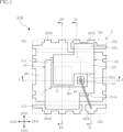
- FIG. 1 is a plan view showing a semiconductor device according to a first embodiment, in which a sealing resin is shown by imaginary lines.
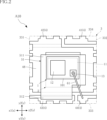
- FIG. 2 is a plan view of FIG. 1 with one of the two conductive plates (the upper conductive plate) omitted.
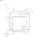
- FIG. 3 is a plan view of FIG. 2 in which the switching elements and connecting members are omitted.
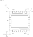
- FIG. 4 is a plan view of FIG. 3 with the other of the two conductive plates (the lower conductive plate) omitted.
- FIG. 5 is a bottom view showing the semiconductor device according to the first embodiment.
- FIG. 6 is a front view showing the semiconductor device according to the first embodiment.
- FIG. 7 is a rear view showing the semiconductor device according to the first embodiment.
- FIG. 1 is a plan view showing a semiconductor device according to a first embodiment, in which a sealing resin is shown by imaginary lines.
- FIG. 2 is a plan view of FIG. 1 with one of the two conductive plates (the upper conductive plate) omitted.
- FIG. 8 is a left side view showing the semiconductor device according to the first embodiment.
- FIG. 9 is a right side view showing the semiconductor device according to the first embodiment.
- FIG. 10 is a cross-sectional view taken along line XX in FIG.
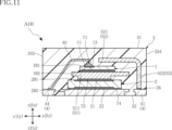
- FIG. 11 is a cross-sectional view taken along line XI-XI of FIG.
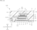
- FIG. 12 is a cross-sectional view taken along line XII-XII in FIG.
- FIG. 13 is a diagram illustrating an example of a circuit configuration of an electronic device including the semiconductor device according to the first embodiment.
- FIG. 14 is a diagram showing an example of a planar layout of an electronic device including the semiconductor device according to the first embodiment.
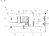
- FIG. 15 is a diagram in which the semiconductor device, the capacitor, the inductor, and the drive circuit in FIG.
- FIG. 16 is a plan view showing a semiconductor device according to a modification of the first embodiment, in which a sealing resin is indicated by imaginary lines.
- FIG. 17 is a plan view of FIG. 16 in which one of the two conductive plates (the upper conductive plate) is omitted.
- FIG. 18 is a plan view of FIG. 17 with the semiconductor elements omitted.
- FIG. 19 is a plan view of FIG. 18 in which the other of the two conductive plates (the lower conductive plate) is omitted.
- FIG. 20 is a bottom view showing a semiconductor device according to a modification of the first embodiment.
- FIG. 21 is a cross-sectional view taken along line XXI-XXI in FIG. FIG.
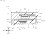
- FIG. 22 is a cross-sectional view taken along line XXII-XXII in FIG.
- FIG. 23 is a plan view showing the semiconductor device according to the second embodiment, in which the sealing resin is shown by imaginary lines.
- FIG. 24 is a plan view of FIG. 23 in which one of the two conductive plates (the upper conductive plate) is omitted.
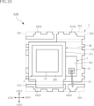
- FIG. 25 is a plan view of FIG. 24 with the semiconductor elements omitted.
- FIG. 26 is a plan view of FIG. 25 in which the other of the two conductive plates (the lower conductive plate) is omitted.
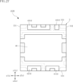
- FIG. 27 is a bottom view showing the semiconductor device according to the second embodiment.
- FIG. 28 is a cross-sectional view taken along line XXVIII-XXVIII in FIG. FIG.
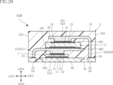
- FIG. 29 is a cross-sectional view taken along line XXIX-XXIX in FIG.
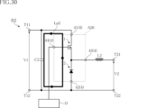
- FIG. 30 is a diagram illustrating an example of a circuit configuration of an electronic device including the semiconductor device according to the second embodiment.
- FIG. 31 is a diagram showing an example of a planar layout of an electronic device including the semiconductor device according to the second embodiment.
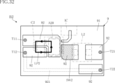
- FIG. 32 is a diagram in which the semiconductor device, the capacitor, the inductor, and the drive circuit in FIG. 31 are shown by imaginary lines.
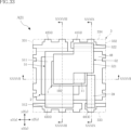
- FIG. 33 is a plan view showing a semiconductor device according to a modification of the second embodiment, in which a sealing resin is indicated by imaginary lines.
- FIG. 34 is a plan view of FIG. 33 in which one of the three conductive plates (the upper conductive plate) is omitted.
- FIG. 35 is a plan view of FIG. 34 with the switching elements omitted.
- FIG. 36 is a plan view of FIG. 35 in which other conductive plates (including the lower conductive plate) are omitted.
- FIG. 37 is a cross-sectional view taken along line XXXVII-XXXVII in FIG. 38 is a cross-sectional view taken along line XXXVIII-XXXVIII in FIG. 33.
- FIG. FIG. 39 is a cross-sectional view taken along line XXXIX-XXXIX in FIG.
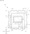
- FIG. 40 is a plan view showing the semiconductor device according to the third embodiment, in which the sealing resin is indicated by imaginary lines.
- FIG. 41 is a plan view of FIG. 40 with the two conductive plates omitted.
- FIG. 42 is a bottom view showing the semiconductor device according to the third embodiment.
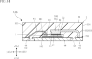
- FIG. 43 is a cross-sectional view taken along line XLIII-XLIII in FIG.
- FIG. 44 is a cross-sectional view taken along line XLIV-XLIV in FIG.
- FIG. 45 is a cross-sectional view taken along line XLV-XLV in FIG.
- FIG. 46 is a plan view showing a semiconductor device according to a modification of the third embodiment, in which the sealing resin is indicated by imaginary lines.
- FIG. 47 is a plan view of FIG. 46 with the conductive plates omitted.
- FIG. 48 is a bottom view showing a semiconductor device according to a modification of the third embodiment.
- FIG. 49 is a cross-sectional view taken along line XLIX-XLIX in FIG.
- FIG. 50 is a cross-sectional view taken along line LL in FIG.
- FIG. 51 is a cross-sectional view taken along line LI-LI in FIG.
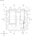
- FIG. 52 is a plan view showing the semiconductor device according to the fourth embodiment, in which the sealing resin is indicated by imaginary lines.
- FIG. 53 is a plan view of FIG. 52 with the two conductive plates omitted.
- FIG. 54 is a bottom view showing the semiconductor device according to the fourth embodiment.
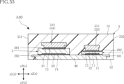
- FIG. 55 is a cross-sectional view taken along the line LV-LV in FIG.
- FIG. 56 is a cross-sectional view taken along line LVI-LVI in FIG.
- FIG. 57 is a cross-sectional view taken along line LVII-LVII in FIG.
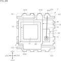
- FIG. 58 is a plan view showing a semiconductor device according to a modification of the fourth embodiment, in which the sealing resin is indicated by imaginary lines.
- FIG. 59 is a plan view of FIG. 58 with the conductive plates omitted.
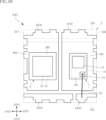
- FIG. 60 is a bottom view showing a semiconductor device according to a modification of the fourth embodiment.
- FIG. 61 is a cross-sectional view taken along line LXI--LXI in FIG.
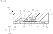
- FIG. 62 is a cross-sectional view taken along line LXII-LXII in FIG.
- FIG. 63 is a cross-sectional view taken along line LXIII--LXIII in FIG.
- FIG. 64 is a plan view showing a semiconductor device according to a modified example, in which the sealing resin and one of the two conductive plates (the upper conductive plate) are omitted.
- FIG. 65 is a plan view showing a semiconductor device according to another modified example, in which the sealing resin and one of the two conductive plates (the upper conductive plate) are omitted.
- FIG. 66 is a diagram showing an example of a planar layout of an electronic device including the semiconductor device of FIG. 64.
- FIG. FIG. 67 is a diagram showing an example of a planar layout of an electronic device including the semiconductor device of FIG. 65.
- FIG. FIG. 65 is a diagram showing an example of a planar layout of an electronic device including the semiconductor device of FIG. 65.
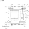
- FIG. 68 is a plan view showing a semiconductor device according to another modified example, in which the sealing resin and one of the two conductive plates (the upper conductive plate) are omitted.
- FIG. 69 is a plan view showing a semiconductor device according to another modified example, in which the sealing resin and one of the two conductive plates (the upper conductive plate) are omitted.
- FIG. 70 is a plan view showing a semiconductor device according to another modified example.
- FIG. 71 is a cross-sectional view taken along line LXXI-LXXI in FIG.
- an object A is formed on an object B
- an object A is formed on (an object B)
- an object A is formed directly on an object B
- an object A is formed on an object B with another object interposed between the object A and the object B” unless otherwise specified.
- an object A is disposed on an object B” and “an object A is disposed on (an object B)” include “an object A is disposed directly on an object B” and “an object A is disposed on (an object B) with another object interposed between the object A and the object B” unless otherwise specified.
- an object A is located on (an object B) includes “an object A is in contact with an object B and is located on (an object B)” and “an object A is located on (an object B) with another object interposed between the object A and the object B".
- an object A overlaps an object B includes “an object A overlaps the entire object B” and “an object A overlaps a part of an object B” unless otherwise specified.
- an object A (its material) contains a certain material C includes “an object A (its material) is made of a certain material C” and "an object A (its material) is mainly composed of a certain material C.”
- First embodiment: 1 to 12 show a semiconductor device A10 according to a first embodiment.
- the semiconductor device A10 includes a switching element 1, a semiconductor element 2, a sealing resin 3, a plurality of terminals 4, a die pad 48, two conductive plates 51 and 52, a connection member 61, and a plurality of bonding materials 71 to 76.
- the thickness direction z corresponds to the thickness direction of the semiconductor device A10.
- the first direction y is perpendicular to the thickness direction z.
- the second direction x is perpendicular to the thickness direction z and the first direction y.
- the terms "top,” “bottom,” “upper,” “lower,” “top surface,” and “bottom surface” indicate the relative positional relationship of each component, etc. in the thickness direction z, and are not necessarily terms that define the relationship with the direction of gravity.
- the semiconductor device A10 is a type that is surface-mounted on a circuit board (mounting board 9, described below) of an electric device, an electric vehicle, or the like.
- the semiconductor device A10 is used, for example, in a DC/DC converter.
- the semiconductor device A10 is rectangular when viewed in the thickness direction z.
- the size of the semiconductor device A10 when viewed in the thickness direction z is not limited in any way, but is, for example, 3.3 mm square.
- the thickness of the semiconductor device A10 (dimension in the thickness direction z) is also not limited in any way, but is, for example, 1.5 mm.
- the switching element 1 is, for example, a MOSFET.
- the switching element 1 may be a transistor other than a MOSFET, such as a field effect transistor including a metal-insulator-semiconductor FET (MISFET) or a high electron mobility transistor (HEMT), or a bipolar transistor such as an IGBT.
- the switching element 1 may also be a thyristor instead of a transistor.
- the switching element 1 is rectangular when viewed in the thickness direction z.
- the size of the switching element 1 when viewed in the thickness direction z is not limited in any way, but for example, the long side is 1.6 mm and the short side is 1.1 mm.
- the semiconductor device A10 as shown in FIGS.
- the thickness (dimension in the thickness direction z) of the switching element 1 is not limited in any way, but is, for example, 0.15 mm.
- the switching element 1 has a main element surface 101 and a back element surface 102. As shown in Figures 10 to 12, the main element surface 101 and the back element surface 102 are spaced apart from each other in the thickness direction z. In the semiconductor device A10, the main element surface 101 faces upward in the thickness direction z (z2 side), and the back element surface 102 faces downward in the thickness direction z (z1 side).
- the switching element 1 has a plurality of electrodes 11, 12, and 13. As shown in Figs. 10 to 12, the electrode 11 is disposed on the back surface 102 of the element, and as shown in Fig. 10, the two electrodes 12 and 13 are disposed on the main surface 101 of the element. In an example in which the switching element 1 is a MOSFET, the electrode 11 is the drain, the electrode 12 is the source, and the electrode 13 is the gate.
- the drain, the source, and the gate of the MOSFET can be replaced with the corresponding electrodes of the other transistor (for example, in the case where an IGBT is used as the switching element 1, the electrode 11 corresponds to the collector, the electrode 12 corresponds to the emitter, and the electrode 13 corresponds to the base).
- the switching element 1 electrical conduction occurs between the electrodes 11 and 12 in response to a drive signal (gate signal) input to the electrode 13.
- the electrode 11 is an example of a "first electrode”
- the electrode 12 is an example of a "second electrode”
- the electrode 13 is an example of a "third electrode".
- the semiconductor element 2 is, for example, a Schottky Barrier Diode (SBD).
- the semiconductor element 2 may be another diode other than an SBD.
- the semiconductor element 2 is rectangular when viewed in the thickness direction z.
- the size of the semiconductor element 2 when viewed in the thickness direction z is not limited, but is, for example, 1.7 mm square. Therefore, in the illustrated example, the semiconductor element 2 is larger than the switching element 1 when viewed in the thickness direction z.
- the thickness (dimension in the thickness direction z) of the semiconductor element 2 is not limited, but is, for example, 0.26 mm. Therefore, in the illustrated example, the semiconductor element 2 is thicker than the switching element 1.
- the size relationship between the switching element 1 and the semiconductor element 2 is appropriately changed according to the specifications of the semiconductor device A10 (the specifications of the switching element 1 and the semiconductor element 2).
- the semiconductor element 2 has an element principal surface 201 and an element rear surface 202. As shown in Figures 10 to 12, the element principal surface 201 and the element rear surface 202 are spaced apart from each other in the thickness direction z. In the semiconductor device A10, the element principal surface 201 faces upward in the thickness direction z (z2 side), and the element rear surface 202 faces downward in the thickness direction z (z1 side).
- the semiconductor element 2 has multiple electrodes 21, 22. As shown in Figures 10 to 12, electrode 21 is disposed on the element's main surface 201, and electrode 22 is disposed on the element's back surface 202. In an example in which the semiconductor element 2 is an SBD, electrode 21 is an anode, and electrode 22 is a cathode. When a forward voltage is applied between electrodes 21 and 22 in the semiconductor element 2, a forward current flows from electrode 21 to electrode 22. Electrode 21 is an example of a "fourth electrode,” and electrode 22 is an example of a "fifth electrode.”
- the switching element 1 and the semiconductor element 2 overlap each other when viewed in the thickness direction z.
- the semiconductor element 2 is disposed below (on the z1 side) the switching element 1 in the thickness direction z.
- the electrode 11 (drain) of the switching element 1 and the electrode 21 (anode) of the semiconductor element 2 are electrically connected inside the sealing resin 3.
- the sealing resin 3 covers the switching element 1 and the semiconductor element 2.
- the sealing resin 3 covers a portion of each of the multiple terminals 4, a portion of the die pad 48, the two conductive plates 51, 52, the connection member 61, and the multiple bonding materials 71-76.
- the sealing resin 3 is rectangular when viewed in the thickness direction z.
- the sealing resin 3 contains, for example, an insulating resin.
- the insulating resin is, for example, an epoxy resin.
- the sealing resin 3 has a resin main surface 31, a resin back surface 32, and multiple resin side surfaces 331 to 334. As shown in Figures 6 to 12, the resin main surface 31 and the resin back surface 32 are spaced apart in the thickness direction z. The resin main surface 31 faces the z2 side of the thickness direction z, and the resin back surface 32 faces the z1 side of the thickness direction z. The resin main surface 31 and the resin back surface 32 are each flat. Each of the multiple resin side surfaces 331 to 334 is disposed between the resin main surface 31 and the resin back surface 32 in the thickness direction z, and is connected to the resin main surface 31 and the resin back surface 32. As shown in Figures 1 to 7 and 10, the two resin side surfaces 331, 332 are spaced apart in the second direction x.
- the resin side surface 331 faces the x1 side of the second direction x, and the resin side surface 332 faces the x2 side of the second direction x.
- the two resin side surfaces 333, 334 are spaced apart in the first direction y.
- the resin side surface 333 faces the y1 side of the first direction y, and the resin side surface 334 faces the y2 side of the first direction y.
- Each of the multiple resin side surfaces 331 to 334 is flat.
- each of the multiple terminals 4 includes, for example, copper.
- the multiple terminals 4 are formed, for example, from a lead frame.
- the multiple terminals 4 include a first terminal 41, a second terminal 42, a third terminal 43, and a fourth terminal 44.
- the first terminal 41 is electrically connected to electrode 12 (source).
- the second terminal 42 is electrically connected to electrode 22 (cathode).
- the third terminal 43 is electrically connected to electrode 11 (drain) and electrode 21 (anode). Thus, the third terminal 43 is a common terminal for electrodes 11 and 21.
- the fourth terminal 44 is electrically connected to electrode 13 (gate).
- the first terminal 41 and the second terminal 42 are adjacent to each other in the second direction x.
- the first terminal 41 is located on the x2 side of the second terminal 42 in the second direction x.
- the first terminal 41 may be located on the x1 side of the second terminal 42 in the second direction x.
- the first terminal 41 and the second terminal 42 are each located on the y2 side of the first direction y with respect to the die pad 48.
- the first terminal 41 and the second terminal 42 are partially exposed on each of the resin back surface 32 and the resin side surface 334.
- the third terminal 43 and the fourth terminal 44 are adjacent to each other in the second direction x.
- the fourth terminal 44 is located on the x2 side of the third terminal 43 in the second direction x.
- the fourth terminal 44 may be located on the x1 side of the third terminal 43 in the second direction x.
- the third terminal 43 and the fourth terminal 44 are each located on the y1 side of the first direction y with respect to the die pad 48.
- the third terminal 43 and the fourth terminal 44 are each partially exposed on each of the resin back surface 32 and the resin side surface 333.
- the third terminal 43 overlaps the second terminal 42 when viewed in the first direction y.
- the fourth terminal 44 overlaps the first terminal 41 when viewed in the first direction y.
- the die pad 48 supports the switching element 1 and the semiconductor element 2. As shown in Figures 10 to 12, the semiconductor element 2 is mounted on the die pad 48, and the electrode 22 (cathode) is joined thereto. As shown in Figure 4, the second terminal 42 is connected to the die pad 48. The second terminal 42 and the die pad 48 are integrally formed. With this configuration, the second terminal 42 is electrically connected to the electrode 22 (cathode) via the die pad 48.
- the shape of the die pad 48 when viewed in the thickness direction z is not limited to the example shown in the figure.
- the two conductive plates 51, 52 are each made of a metal material.
- the metal material includes, for example, copper.
- the two conductive plates 51, 52 are not limited to being made of a metal material, and may be made of any material that conducts electricity.
- the two conductive plates 51, 52 are each covered with sealing resin 3.
- the conductive plate 51 includes a joint 511 and an extension 512, as shown in FIG. 3 and FIG. 12.
- the joint 511 and the extension 512 are integrally formed.
- the joint 511 is sandwiched between the switching element 1 and the semiconductor element 2.
- the joint 511 is bonded to each of the electrode 11 (drain) and the electrode 21 (anode).
- the joint 511 is disposed downward in the thickness direction z (z1 side) with respect to the switching element 1, and disposed upward in the thickness direction z (z2 side) with respect to the semiconductor element 2.
- the joint 511 extends along a plane perpendicular to the thickness direction z. As shown in FIG. 10 to FIG. 12, the joint 511 partially protrudes downward in the thickness direction z (z1 side).
- the protruding portion is bonded to the electrode 21.
- the joint 511 may be partially bent downward in the thickness direction z (z1 side), and the bent portion may be bonded to the electrode 21.
- the extension portion 512 is joined to the third terminal 43.
- the extension portion 512 extends downward in the thickness direction z (toward the z1 side) from the joint portion 511.
- the conductive plate 51 electrically connects the third terminal 43 to each of the electrodes 11 and 21.
- the conductive plate 52 includes a joint 521 and an extension 522, as shown in FIG. 1 and FIG. 10 to FIG. 12.
- the joint 521 and the extension 522 are integrally formed.
- the joint 521 is disposed above the switching element 1 in the thickness direction z (z2 side).
- the conductive plate 52 is joined to the electrode 12 (source) of the switching element 1.
- the joint 521 extends along a plane perpendicular to the thickness direction z. As shown in FIG. 10 and FIG. 12, the joint 521 partially protrudes downward in the thickness direction z (z1 side). In this embodiment, this protruding portion is joined to the electrode 12.
- the joint 521 may be partially bent downward in the thickness direction z (z1 side), and the bent portion may be joined to the electrode 12.
- a notch 521a is formed in the joint 521. Due to the notch 521a, the electrode 13 of the switching element 1 does not overlap the conductive plate 52 when viewed in the thickness direction z. To improve heat dissipation, the upper surface of the joint 521 (the surface facing the z2 side in the thickness direction z) may be exposed from the resin main surface 31 of the sealing resin 3. The extension portion 522 extends downward (to the z1 side) in the thickness direction z from the joint 521. The conductive plate 52 electrically connects the second terminal 42 and the electrode 12.
- connection member 61 electrically connects two parts that are spaced apart from each other.
- the connection member 61 is a bonding wire.
- the constituent material of the connection member 61 is not limited in any way, but includes, for example, gold, aluminum, silver, or copper.
- the connection member 61 is joined to the electrode 13 (gate) and the fourth terminal 44. With this configuration, the fourth terminal 44 is electrically connected to the electrode 13 via the connection member 61.
- Each of the multiple bonding materials 71-76 electrically connects two parts.
- Each of the multiple bonding materials 71-76 is, for example, solder.
- the multiple bonding materials 71-76 may be sintered metal or a metal paste material instead of solder.
- the multiple bonding materials 71-76 are omitted from illustration in each of Figures 1-5.
- the bonding material 71 is for bonding the electrode 11 (drain) of the switching element 1.
- the bonding material 71 is interposed between the electrode 11 and the conductive plate 51 (bonding portion 511) and electrically bonds them together.
- the bonding material 72 is for bonding the electrode 12 (source) of the switching element 1.
- the bonding material 72 is interposed between the electrode 12 and the conductive plate 52 (bonding portion 521) and electrically bonds them together.
- the bonding material 73 is for bonding the electrode 21 (anode) of the semiconductor element 2.
- the bonding material 73 is interposed between the electrode 21 and the conductive plate 51 (bonding portion 511) and electrically bonds them.
- the bonding material 74 is for bonding the electrode 22 (cathode) of the semiconductor element 2.
- the bonding material 74 is interposed between the electrode 22 and the die pad 48, and electrically bonds them together.
- the bonding material 75 is for bonding the conductive plate 51 (extension 512). In the semiconductor device A10, as shown in FIG. 12, the bonding material 75 is interposed between the conductive plate 51 (extension 512) and the third terminal 43, and electrically bonds them.
- the bonding material 76 is for bonding the conductive plate 52 (extension 522).
- the bonding material 76 is interposed between the conductive plate 52 (extension 522) and the second terminal 42, and electrically bonds them.
- FIGS. 13 to 15 show an electronic device B1 that includes a semiconductor device A10. As shown in these figures, in addition to the semiconductor device A10, the electronic device B1 includes a mounting substrate 9, a capacitor C1, an inductor L1, and a drive circuit D.
- the electronic device B1 is electrically connected to the drain (electrode 11) of the semiconductor device A10 and the switching element 1 and the anode (electrode 21) of the semiconductor element 2. These connection points are conductive to the third terminal 43.
- the inductor L1 is connected between the third terminal 43 and the input terminal T11.
- One electrode of the capacitor C1 is electrically connected to the second terminal 42 of the semiconductor device A10, and the other electrode of the capacitor C1 is electrically connected to the first terminal 41 of the semiconductor device A10.
- the capacitor C1 is connected to the cathode (electrode 22) of the semiconductor element 2 and the source (electrode 12) of the switching element 1, respectively.
- the capacitor C1 is connected to a pair of output terminals T21 and T22.
- the capacitor C1 functions as an output capacitor arranged on the output side of the semiconductor device A10.
- the electronic device B1 switching element 1 and semiconductor element 2
- the potential of the second terminal 42 is higher than the potential of the first terminal 41, and the semiconductor element 2 is connected to the higher potential side than the switching element 1.
- the electronic device B1 constitutes a boost circuit (boost chopper circuit).
- the electronic device B1 boosts the voltage V1 applied to a pair of input terminals T11, T12 to a voltage V2 by the switching operation of the switching element 1.
- the boosted voltage V2 is then output from a pair of output terminals T21, T22.
- the input terminal T12 and the output terminal T22 are, for example, connected to ground.
- the drive circuit D generates a drive signal for the switching element 1 and outputs the drive signal to the gate (electrode 13) of the switching element 1.
- the drive circuit D is formed, for example, by an integrated circuit (IC).
- the mounting board 9 is mounted on each module of an electrical product, an electric vehicle, or the like.
- the mounting board 9 is, for example, a printed circuit board.
- the mounting board 9 may not be a printed circuit board, but may be a semiconductor board, a glass board, a resin board, or the like.
- the mounting board 9 includes a base material 91 and a wiring pattern 92.
- the substrate 91 supports the semiconductor device A10, the capacitor C1, the inductor L1, the drive circuit D, and the like.
- the substrate 91 is made of glass epoxy resin.
- the wiring pattern 92 is formed on the substrate 91.
- the constituent material of the wiring pattern 92 is not limited in any way, but may include, for example, copper.
- the constituent material of the wiring pattern 92 is not limited to copper, but may include gold, silver, or aluminum.
- the wiring pattern 92 electrically connects the semiconductor device A10, the capacitor C1, the inductor L1, and the drive circuit D so that the electronic device B1 has the circuit configuration shown in FIG. 13.
- the wiring pattern 92 includes a back wiring 921.
- the back wiring 921 is conductive to the wiring pattern 92 formed on the upper surface of the substrate 91, for example, through a through via that penetrates the substrate 91.
- the wiring may be a wiring that passes inside the substrate 91.
- the wiring pattern 92 may be connected to the input terminal T12 and the output terminal T22 without including the back wiring 921.
- the functions and effects of the semiconductor device A10 and the electronic device B1 are as follows.
- the electrode 11 of the switching element 1 and the electrode 21 of the semiconductor element 2 are electrically connected inside the sealing resin 3.
- the electrode 11 is the drain, and the electrode 21 is the anode.
- the first terminal 41 and the second terminal 42 are adjacent to each other.
- the first terminal 41 is electrically connected to the electrode 12 of the switching element 1
- the second terminal 42 is electrically connected to the electrode 22 of the semiconductor element 2.
- the electrode 12 is a source
- the electrode 22 is a cathode.
- the semiconductor device A10 By shortening this distance, when the semiconductor device A10 is used as a boost circuit and the electrodes 12 and 22 are connected to the capacitor C1, the distance of the current loop Lp1 (see Figures 13 and 15) passing through the capacitor C1 can be shortened. Reducing the distance of the current loop Lp1 is effective in reducing noise. Therefore, the semiconductor device A10 can further reduce noise.
- the switching element 1 and the semiconductor element 2 overlap each other when viewed in the thickness direction z.
- the switching element 1 and the semiconductor element 2 are stacked in the thickness direction z. Therefore, the area of the semiconductor device A10 when viewed in the thickness direction z can be reduced.
- switching element 1 is arranged above semiconductor element 2 in the thickness direction z (z2 side).
- semiconductor element 2 is larger than switching element 1.
- switching element 1 and semiconductor element 2 are stacked, it is possible to stably place the one arranged above in the thickness direction z (z2 side) (switching element 1 in semiconductor device A10).
- tilting and tipping over of switching element 1 during manufacturing can be suppressed, thereby suppressing manufacturing defects of semiconductor device A10. Therefore, semiconductor device A10 can improve manufacturing quality.
- the semiconductor device A10 the first terminal 41 and the second terminal 42 are exposed from the resin side surface 334, and the third terminal 43 and the fourth terminal 44 are exposed from the resin side surface 333. With this configuration, it is possible to appropriately secure the area of each of the first terminal 41, the second terminal 42, and the third terminal 43. For example, a main current (current corresponding to the power supply voltage) in a boost circuit flows through the first terminal 41, the second terminal 42, and the third terminal 43, and the allowable current of the semiconductor device A10 is reduced according to the area of the first terminal 41, the second terminal 42, and the third terminal 43. Therefore, the semiconductor device A10 can suppress the reduction in the allowable current.
- Modification of the first embodiment show a semiconductor device A11 according to a modified example of the first embodiment.
- the semiconductor device A11 is different from the semiconductor device A10 in the following respects.
- the switching element 1 is disposed on the z2 side of the conductive plate 51 (joint 511) in the thickness direction z
- the semiconductor element 2 is disposed on the z1 side of the conductive plate 51 (joint 511) in the thickness direction z.
- the switching element 1 is disposed with the element main surface 101 facing downward (z1 side) in the thickness direction z.
- the semiconductor element 2 is disposed with the element main surface 201 facing downward (z1 side) in the thickness direction z.
- the semiconductor device A11 like the semiconductor device A10, is provided in the electronic device B1 as a part of a boost circuit (see FIGS. 13 to 15).
- the electrode 13 (gate) of the switching element 1 is joined to the fourth terminal 44.
- a notch 481 is formed in the die pad 48.
- the notch 481 extends the fourth terminal 44 to a region overlapping the electrode 13 of the switching element 1 when viewed in the thickness direction z. This makes it possible to join the electrode 13 of the switching element 1 to the fourth terminal 44. In this way, by directly joining the electrode 13 to the fourth terminal 44, the fourth terminal 44 is electrically connected to the electrode 13, so the semiconductor device A11 does not include a connection member 61.
- the electrode 12 (source) of the switching element 1 is joined to the die pad 48. Therefore, as shown in FIGS.
- the switching element 1 is flip-chip mounted across the die pad 48 and the fourth terminal 44.
- the electrode 11 (drain) of the switching element 1 is joined to the conductive plate 51 (joint 511). This allows the third terminal 43 to be electrically connected to the electrode 11 via the conductive plate 51.
- the second terminal 42 is not connected to the die pad 48, and the first terminal 41 is connected to the die pad 48.
- the first terminal 41 and the die pad 48 are integrally formed. Therefore, the first terminal 41 is electrically connected to the electrode 12 (source) via the die pad 48.
- the element main surface 201 of the semiconductor element 2 faces the conductive plate 51 (joint 511), and the electrode 21 (anode) of the semiconductor element 2 is joined to the conductive plate 51 (joint 511).
- the third terminal 43 is electrically connected to the electrode 21 through the conductive plate 51.
- the third terminal 43 is electrically connected to the electrode 11 (drain) through the conductive plate 51, so the third terminal 43 is a common terminal for the electrode 11 (drain) and the electrode 21 (anode).
- the element back surface 202 of the semiconductor element 2 faces the conductive plate 52 (joint 521), and the electrode 22 (cathode) of the semiconductor element 2 is joined to the conductive plate 52 (joint 521). As a result, the second terminal 42 is electrically connected to the electrode 22 through the conductive plate 52.
- bonding material 72 is interposed between electrode 12 (source) and die pad 48, electrically connecting them.
- Bonding material 74 is interposed between electrode 22 (cathode) and conductive plate 52 (bonding portion 521), electrically connecting them.
- Bonding material 76 is interposed between conductive plate 52 (extension portion 522) and second terminal 42, electrically connecting them.
- the semiconductor device A11 also includes a bonding material 77.
- the bonding material 77 is for bonding the electrode 13 (gate). As shown in FIG. 21, the bonding material 77 is interposed between the electrode 13 and the fourth terminal 44, and electrically bonds them together.
- the multiple bonding materials 71 to 77 are not shown in FIG. 16 to FIG. 19.
- the semiconductor device A11 like the semiconductor device A10, the electrode 11 (drain) of the switching element 1 and the electrode 21 (anode) of the semiconductor element 2 are electrically connected inside the sealing resin 3. Therefore, like the semiconductor device A10, the semiconductor device A11 can reduce noise. Furthermore, like the semiconductor device A10, in the semiconductor device A11, the first terminal 41 that is conductive to the electrode 12 (source) of the switching element 1 and the second terminal 42 that is conductive to the electrode 22 (cathode) of the semiconductor element 2 are adjacent to each other. Therefore, like the semiconductor device A10, the semiconductor device A11 can further reduce noise. In addition, the semiconductor device A11 has a common configuration with the semiconductor device A10, and thus achieves the same effects as the semiconductor device A10.
- the switching element 1 is arranged with the element main surface 101 facing the z1 side in the thickness direction z. In this configuration, the switching element 1 is flip-chip mounted. For this reason, the semiconductor device A11 does not include a connection member 61. Therefore, compared to the semiconductor device A10, the semiconductor device A11 can eliminate the process of forming the connection member 61 (wire bonding process).
- the switching element 1 is mounted on the die pad 48.
- the electrode 12 of the switching element 1 is bonded to the die pad 48.
- the electrode 12 is the source.
- the semiconductor device A11 is used in a boost circuit, and for example, the electrode 12 of the switching element 1 is grounded. Therefore, the electrode 12 of the switching element 1 is connected to the ground of the mounting substrate 9 via the die pad 48. This is effective in improving the heat dissipation of the semiconductor device A11. In other words, the semiconductor device A11 can improve the heat dissipation more than the semiconductor device A10.
- Second embodiment: 23 to 29 show a semiconductor device A20 according to the second embodiment.
- the semiconductor device A20 is different from the semiconductor device A10 in the following respects.
- the first terminal 41 is conductive to the electrode 11 (drain) of the switching element 1, not the electrode 12 (source) of the switching element 1.
- the second terminal 42 is conductive to the electrode 21 (anode) of the semiconductor element 2, not the electrode 22 (cathode) of the semiconductor element 2.
- Third, the third terminal 43 is conductive to the electrode 12 (source) of the switching element 1 and the electrode 22 (cathode) of the semiconductor element 2, not the electrode 11 (drain) of the switching element 1 and the electrode 21 (anode) of the semiconductor element 2.
- the electrode 11 is an example of a "second electrode”
- the electrode 12 is an example of a "first electrode”
- the electrode 13 is an example of a "third electrode”.
- the electrode 21 is an example of a "fifth electrode”
- the electrode 22 cathode is an example of a "fourth electrode.”
- the first terminal 41 is connected to the die pad 48 and is formed integrally with the die pad 48.
- the electrode 11 (drain) of the switching element 1 is bonded to the die pad 48.
- the die pad 48 and the electrode 11 are bonded by a bonding material 71. This allows the first terminal 41 to be electrically connected to the electrode 11 (drain).
- the conductive plate 52 (extension 522) is joined to the second terminal 42. As shown in FIG. 29, the conductive plate 52 (extension 522) and the second terminal 42 are joined by a bonding material 76.
- the electrode 21 (anode) of the semiconductor element 2 is joined to the conductive plate 52 (bonding portion 521). As shown in FIGS. 28 and 29, the conductive plate 52 (bonding portion 521) and the electrode 21 are joined by a bonding material 73. This allows the second terminal 42 to be electrically connected to the electrode 21 (anode).
- the conductive plate 51 (extension 512) is joined to the third terminal 43.
- the conductive plate 51 (extension 512) and the third terminal 43 are joined by a bonding material 75.
- the electrode 12 (source) of the switching element 1 and the electrode 22 (cathode) of the semiconductor element 2 are joined to the conductive plate 51 (bonding portion 511).
- the conductive plate 51 (bonding portion 511) and the electrode 12 are joined by a bonding material 72
- the conductive plate 51 (bonding portion 511) and the electrode 22 are joined by a bonding material 74. This allows the third terminal 43 to be electrically connected to the electrode 12 (source) and the electrode 22 (cathode).
- connection member 61 is joined to the fourth terminal 44, and the connection member 61 is joined to the electrode 13 (gate) of the switching element 1.
- the fourth terminal 44 is electrically connected to the electrode 13 (gate).
- the switching element 1 is positioned slightly offset in the second direction x with respect to the two conductive plates 51, 52 and the semiconductor element 2.
- the electrode 13 of the switching element 1 does not overlap any of the two conductive plates 51, 52 or the semiconductor element 2 when viewed in the thickness direction z, making it possible to join the connection member 61 to the electrode 13.
- FIGS. 30 to 32 show an electronic device B2 that includes a semiconductor device A20.
- the electronic device B2 includes a mounting substrate 9, a capacitor C2, an inductor L2, and a drive circuit D.
- the source (electrode 12) of the switching element 1 and the cathode (electrode 22) of the semiconductor element 2 are electrically connected in the semiconductor device A20. These connection points are conductive to the third terminal 43.
- the inductor L2 is connected between the third terminal 43 and the output terminal T21.
- One electrode of the capacitor C2 is electrically connected to the first terminal 41 of the semiconductor device A20, and the other electrode of the capacitor C2 is electrically connected to the second terminal 42 of the semiconductor device A20.
- the capacitor C2 is connected to the drain (electrode 11) of the switching element 1 and the anode (electrode 21) of the semiconductor element 2, respectively.
- the capacitor C2 is connected to a pair of input terminals T11, T12.
- the capacitor C2 functions as an input capacitor arranged on the input side of the semiconductor device A20.
- the electronic device B2 switching element 1 and semiconductor element 2
- the potential of the first terminal 41 is higher than the potential of the second terminal 42
- the switching element 1 is connected to the higher potential side than the semiconductor element 2.
- the electronic device B2 constitutes a step-down circuit (step-down chopper circuit).
- the electronic device B2 steps down the voltage V1 applied to a pair of input terminals T11, T12 to a voltage V2 by the switching operation of the switching element 1.
- the stepped-down voltage V2 is output from a pair of output terminals T21, T22.
- the input terminal T12 and the output terminal T22 are, for example, connected to ground.
- the functions and effects of the semiconductor device A20 and the electronic device B2 are as follows.
- the electrode 12 of the switching element 1 and the electrode 22 of the semiconductor element 2 are electrically connected inside the sealing resin 3.
- the electrode 12 is the source
- the electrode 22 is the cathode.
- the first terminal 41 and the second terminal 42 are adjacent to each other.
- the first terminal 41 is electrically connected to the electrode 11 of the switching element 1
- the second terminal 42 is electrically connected to the electrode 21 of the semiconductor element 2.
- the electrode 11 is a drain
- the electrode 21 is an anode.
- the semiconductor device A20 By shortening this distance, when the semiconductor device A20 is used as a step-down circuit and the electrodes 11 and 21 are connected to the capacitor C2, the distance of the current loop Lp2 (see Figures 30 and 32) passing through the capacitor C2 can be shortened. Reducing the distance of the current loop Lp2 is effective in reducing noise. Therefore, the semiconductor device A20 can further reduce noise.
- the semiconductor device A20 has a common configuration with the other semiconductor devices A10 and A11, and thus achieves the same effects as the other semiconductor devices A10 and A11.
- Modification of the second embodiment show a semiconductor device A21 according to a modified example of the second embodiment.
- the semiconductor device A21 is different from the semiconductor device A20 in the following respects.
- the switching element 1 is disposed on the z2 side of the conductive plate 51 (joint 511) in the thickness direction z
- the semiconductor element 2 is disposed on the z1 side of the conductive plate 51 (joint 511) in the thickness direction z.
- the switching element 1 is disposed with the element main surface 101 facing the z1 side of the thickness direction z
- the semiconductor element 2 is disposed with the element main surface 201 facing the z1 side of the thickness direction z.
- the semiconductor device A21 like the semiconductor device A20, is provided in the electronic device B2 as a part of a step-down circuit (see FIGS. 30 to 32).
- the bottom view of the semiconductor device A21 and the bottom view of the semiconductor device A10 have the same appearance.
- electrode 11 (drain) of switching element 1 is joined to conductive plate 52 (joint 521) by bonding material 71.
- Electrode 12 of switching element 1 is joined to conductive plate 51 (joint 511) by bonding material 72.
- Electrode 21 of semiconductor element 2 is joined to die pad 48 by bonding material 73.
- Electrode 22 of semiconductor element 2 is joined to conductive plate 51 (joint 511) by bonding material 74.
- the semiconductor device A21 further includes a conductive plate 59.
- the conductive plate 59 is made of, for example, a metal material.
- the metal material includes copper.
- the conductive plate 59 is not limited to being made of a metal material as long as it is electrically conductive.
- the conductive plate 59 is joined to the electrode 13 (gate) of the switching element 1 and the fourth terminal 44, and conducts them. As shown in FIG. 37, the electrode 13 is joined to the conductive plate 59 by a bonding material 77. As shown in FIG. 39, the conductive plate 59 is joined to the fourth terminal 44 by a bonding material 590.
- the bonding material 590 is, for example, solder, sintered metal, or metal paste material.
- the semiconductor device A10 includes an insulating block 591 to support the conductive plate 59 while ensuring insulation from the semiconductor element 2.
- the semiconductor device A21 like the semiconductor device A20, the electrode 12 (source) of the switching element 1 and the electrode 22 (cathode) of the semiconductor element 2 are electrically connected inside the sealing resin 3. Therefore, like the semiconductor device A20, the semiconductor device A21 can reduce noise. Furthermore, like the semiconductor device A20, in the semiconductor device A21, the first terminal 41 that is conductive to the electrode 11 (drain) of the switching element 1 and the second terminal 42 that is conductive to the electrode 21 (anode) of the semiconductor element 2 are adjacent to each other. Therefore, like the semiconductor device A20, the semiconductor device A21 can further reduce noise. In addition, the semiconductor device A21 has a common configuration with the other semiconductor devices A10, A11, and A20, and thus achieves the same effects as the semiconductor devices A10, A11, and A21.
- the semiconductor element 2 is mounted on the die pad 48.
- the electrode 21 of the semiconductor element 2 is bonded to the die pad 48.
- the electrode 21 is an anode.
- the semiconductor device A21 is used in a step-down circuit, and for example, the electrode 21 of the semiconductor element 2 is grounded. Therefore, the electrode 21 of the semiconductor element 2 is connected to the ground of the mounting substrate 9 via the die pad 48. This is effective in improving the heat dissipation of the semiconductor device A21. In other words, the semiconductor device A21 can improve the heat dissipation more than the semiconductor device A20.
- Figures 40 to 45 show a semiconductor device A30 according to the third embodiment.
- the semiconductor device A30 is different from the semiconductor device A10 in the following respect. That is, the switching element 1 and the semiconductor element 2 do not overlap when viewed in the thickness direction z.
- the semiconductor device A30 is used in the electronic device B1 as part of a boost circuit (see Figures 13 to 15).
- the switching element 1 and the semiconductor element 2 are mounted on the die pad 48.
- the switching element 1 is arranged with the element back surface 102 facing the z1 side in the thickness direction z. Therefore, as shown in FIG. 43 and FIG. 44, the element back surface 102 faces the die pad 48, and the electrode 11 (drain) is joined to the die pad 48 by the bonding material 71. As a result, the die pad 48 is electrically connected to the electrode 11.
- the semiconductor element 2 is arranged with the element main surface 201 facing the z1 side in the thickness direction z. Therefore, as shown in FIG. 43 and FIG. 45, the element main surface 201 faces the die pad 48, and the electrode 21 (anode) is joined to the die pad 48 by the bonding material 73. As a result, the die pad 48 is electrically connected to the electrode 21.
- the third terminal 43 is connected to the die pad 48 and is formed integrally with the die pad 48.
- the die pad 48 is conductive to the electrodes 11 and 21, and therefore the third terminal 43 is conductive to the electrodes 11 (drain) and 21 (anode) via the die pad 48.
- the semiconductor device A30 has two conductive plates 53, 54 instead of the two conductive plates 51, 52.
- the two conductive plates 53, 54 are each made of a metal material.
- the metal material includes, for example, copper.
- the two conductive plates 53, 54 are not limited to being made of a metal material, and may be made of any material that conducts electricity.
- the conductive plate 53 includes a joint 531 and an extension 532, as shown in FIG. 40 and FIG. 44.
- the joint 531 and the extension 532 are integrally formed.
- the joint 531 is disposed on the switching element 1. As shown in FIG. 43 and FIG. 44, the joint 531 partially protrudes downward in the thickness direction z (z1 side). In this embodiment, this protruding portion is bonded to the electrode 12 (source) of the switching element 1.
- the joint 531 may be partially bent downward in the thickness direction z (z1 side), and the bent portion may be bonded to the electrode 12.
- the extension 532 is bonded to the first terminal 41.
- the extension 532 extends downward in the thickness direction z (z1 side) from the joint 531.
- the conductive plate 53 electrically connects the first terminal 41 and the electrode 12.
- the conductive plate 54 includes a joint 541 and an extension 542, as shown in FIG. 40 and FIG. 45.
- the joint 541 and the extension 542 are integrally formed.
- the joint 541 is disposed on the semiconductor element 2.
- the joint 541 partially protrudes downward in the thickness direction z (z1 side).
- this protruding portion is bonded to the electrode 22 (cathode) of the semiconductor element 2.
- the joint 541 may be partially bent downward in the thickness direction z (z1 side), and the bent portion may be bonded to the electrode 22.
- the extension 542 is bonded to the second terminal 42.
- the extension 542 extends downward in the thickness direction z (z1 side) from the joint 541.
- the conductive plate 54 electrically connects the second terminal 42 and the electrode 22.
- bonding material 71 is interposed between electrode 11 and die pad 48, electrically connecting them.
- Bonding material 72 is interposed between electrode 12 and conductive plate 53 (joint 531), electrically connecting them.
- Bonding material 73 is interposed between electrode 21 and die pad 48, electrically connecting them.
- Bonding material 74 is interposed between electrode 22 and conductive plate 54 (joint 541), electrically connecting them.
- the semiconductor device A30 further includes two bonding materials 781 and 782.
- the two bonding materials 781 and 782 are, for example, solder.
- the two bonding materials 781 and 782 may be sintered metal or metal paste material instead of solder.
- the bonding material 781 is for bonding the conductive plate 53 (extension 532).
- the bonding material 781 is interposed between the conductive plate 53 (extension 532) and the first terminal 41, and electrically connects them.
- the bonding material 782 is for bonding the conductive plate 54 (extension 542).
- the bonding material 782 is interposed between the conductive plate 54 (extension 542) and the second terminal 42, and electrically connects them.
- the multiple bonding materials 71 to 74, 781, and 782 are omitted from illustration.
- the semiconductor device A30 like the semiconductor device A10, the electrode 11 (drain) of the switching element 1 and the electrode 21 (anode) of the semiconductor element 2 are electrically connected inside the sealing resin 3. Therefore, like the semiconductor device A10, the semiconductor device A30 can reduce noise. Furthermore, like the semiconductor device A10, in the semiconductor device A30, the first terminal 41 that is conductive to the electrode 12 (source) of the switching element 1 and the second terminal 42 that is conductive to the electrode 22 (cathode) of the semiconductor element 2 are adjacent to each other. Therefore, like the semiconductor device A10, the semiconductor device A30 can further reduce noise. In addition, the semiconductor device A30 has a common configuration with the other semiconductor devices A10, A11, A20, and A21, and thus has the same effects as the semiconductor devices A10, A11, A20, and A21.
- switching element 1 and semiconductor element 2 do not overlap each other when viewed in thickness direction z. In this configuration, switching element 1 and semiconductor element 2 are arranged along a plane perpendicular to thickness direction z. Therefore, semiconductor device A30 can have a smaller dimension in thickness direction z than semiconductor device A10.
- Modification of the third embodiment show a semiconductor device A31 according to a modified example of the third embodiment.
- the semiconductor device A31 is different from the semiconductor device A30 in the following respects.
- the switching element 1 is arranged with the element main surface 101 facing the z1 side in the thickness direction z.
- the semiconductor element 2 is arranged with the element back surface 202 facing the z1 side in the thickness direction z.
- the semiconductor device A31 includes two die pads 491 and 492 instead of the die pad 48.
- the semiconductor device A31 does not include the two conductive plates 53 and 54, but includes a conductive plate 55.
- the semiconductor device A31 like the semiconductor device A30, is used in the electronic device B1 as a part of a boost circuit.
- the two die pads 491, 492 are spaced apart from each other. In the example shown in FIG. 47, the two die pads 491, 492 are arranged along the second direction x. The third terminal 43 is not connected to either of the two die pads 491, 492.
- a switching element 1 is mounted on the die pad 491, and an electrode 12 (source) is joined to the die pad 491.
- a first terminal 41 is connected to the die pad 491.
- the first terminal 41 and the die pad 491 are integrally formed. With this configuration, the first terminal 41 is electrically connected to the electrode 12 (source) via the die pad 491.
- a semiconductor element 2 is mounted on the die pad 492, and an electrode 22 (cathode) is bonded to the die pad 492.
- a second terminal 42 is connected to the die pad 492.
- the second terminal 42 and the die pad 492 are integrally formed. With this configuration, the second terminal 42 is electrically connected to the electrode 22 (cathode) via the die pad 492.
- the conductive plates 55 are made of a metal material.
- the metal material includes, for example, copper.
- the conductive plates 55 are not limited to being made of a metal material, and may be made of any material that conducts electricity.
- the conductive plate 55 includes a joint 551 and an extension 552, as shown in FIG. 46 and FIG. 49 to FIG. 51.
- the joint 551 and the extension 552 are integrally formed.
- the joint 551 straddles the switching element 1 and the semiconductor element 2 when viewed in the thickness direction z.
- the joint 551 is joined to the electrode 11 (drain) of the switching element 1 and to the electrode 21 (anode) of the semiconductor element 2. As shown in FIG. 49, the joint 551 partially protrudes downward in the thickness direction z (z1 side), and the protruding portion is joined to the electrode 11 and the electrode 21, respectively.
- the joint 551 may be partially bent downward in the thickness direction z (z1 side), and the bent portion may be joined to the electrode 11 and the electrode 21, respectively.
- the extension 552 is joined to the third terminal 43.
- the extension portion 552 extends downward in the thickness direction z (toward the z1 side) from the joint portion 551.
- the conductive plate 55 electrically connects the third terminal 43 to the electrode 11 and the electrode 21.
- the semiconductor device A31 further includes a bonding material 79.
- the bonding material 79 is, for example, solder.
- the bonding material 79 may be a sintered metal or a metal paste material instead of solder.
- the bonding material 79 is for bonding the conductive plate 55 (extension 552). As shown in FIG. 51, the bonding material 79 is interposed between the conductive plate 55 (extension 552) and the third terminal 43, and electrically connects them.
- the multiple bonding materials 71 to 74, 77, and 79 are omitted from illustration.
- the semiconductor device A31 like the semiconductor device A30, the electrode 11 (drain) of the switching element 1 and the electrode 21 (anode) of the semiconductor element 2 are electrically connected inside the sealing resin 3. Therefore, like the semiconductor device A30, the semiconductor device A31 can reduce noise. Furthermore, like the semiconductor device A30, in the semiconductor device A31, the first terminal 41 that is conductive to the electrode 12 (source) of the switching element 1 and the second terminal 42 that is conductive to the electrode 22 (cathode) of the semiconductor element 2 are adjacent to each other. Therefore, like the semiconductor device A30, the semiconductor device A31 can further reduce noise. In addition, the semiconductor device A31 has a common configuration with the other semiconductor devices A10, A11, A20, A21, and A30, and thus achieves the same effects as the semiconductor devices A10, A11, A20, A21, and A30.
- Fourth embodiment: 52 to 57 show a semiconductor device A40 according to the fourth embodiment.
- the semiconductor device A40 differs from the semiconductor device A30 in the following respects.
- the switching element 1 is arranged with the element main surface 101 facing the z1 side in the thickness direction z.
- the semiconductor element 2 is arranged with the element back surface 202 facing the z1 side in the thickness direction z.
- the semiconductor device A40 is used as a step-down circuit in the electronic device B2 (see FIGS. 30 to 32).
- the electrode 11 (drain) of the switching element 1 is bonded to the conductive plate 53 (bonding portion 531) by a bonding material 71.
- the conductive plate 53 (extension portion 532) is bonded to the first terminal 41 by a bonding material 781, so that the first terminal 41 is conductive to the electrode 11.
- the electrode 12 (source) of the switching element 1 is bonded to the die pad 48 by a bonding material 72.
- the die pad 48 is connected to the third terminal 43, so that the third terminal 43 is conductive to the electrode 12.
- the electrode 13 (gate) of the switching element 1 is bonded to the fourth terminal 44 by a bonding material 77. Therefore, the fourth terminal 44 is conductive to the electrode 13.
- the multiple bonding materials 71 to 74, 781, and 782 are omitted from the illustration.
- the electrode 21 (anode) of the semiconductor element 2 is bonded to the conductive plate 54 (joint portion 541) by a bonding material 73.
- the conductive plate 54 (extension portion 542) is bonded to the second terminal 42 by a bonding material 782, so that the second terminal 42 is conductive to the electrode 21.
- the electrode 22 (cathode) of the semiconductor element 2 is bonded to the die pad 48 by a bonding material 74.
- the die pad 48 is connected to the third terminal 43, so that the third terminal 43 is conductive to the electrode 22.
- the semiconductor device A40 like the semiconductor device A20, the electrode 12 (source) of the switching element 1 and the electrode 22 (cathode) of the semiconductor element 2 are electrically connected inside the sealing resin 3. Therefore, like the semiconductor device A20, the semiconductor device A40 can reduce noise. Furthermore, like the semiconductor device A20, the first terminal 41 that is conductive to the electrode 11 (drain) of the switching element 1 and the second terminal 42 that is conductive to the electrode 21 (anode) of the semiconductor element 2 are adjacent to each other. Therefore, like the semiconductor device A20, the semiconductor device A40 can further reduce noise.
- the semiconductor device A40 has a common configuration with the other semiconductor devices A10, A11, A20, A21, A30, and A31, and thus has the same effects as the semiconductor devices A10, A11, A20, A21, A30, and A31.
- Modification of the fourth embodiment 58 to 63 show a semiconductor device A41 according to a modified example of the fourth embodiment.
- the semiconductor device A41 is different from the semiconductor device A40 in the following respects.
- the switching element 1 is arranged with the element main surface 101 facing the z2 side in the thickness direction z.
- the semiconductor element 2 is arranged with the element back surface 202 facing the z2 side in the thickness direction z.
- the semiconductor device A41 includes two die pads 491 and 492 instead of the die pad 48.
- the semiconductor device A41 does not include the two conductive plates 53 and 54, but includes a conductive plate 55.
- the semiconductor device A41 is used as a step-down circuit in the electronic device B2, similar to the semiconductor device A40.
- the electrode 11 (drain) of the switching element 1 is bonded to the die pad 491 by a bonding material 71.
- the die pad 491 is connected to the first terminal 41, so that the first terminal 41 is conductive to the electrode 11.
- the electrode 12 (source) of the switching element 1 is bonded to the conductive plate 55 (bonding portion 551) by a bonding material 72.
- the conductive plate 55 (extension portion 552) is bonded to the third terminal 43 by a bonding material 79, so that the third terminal 43 is conductive to the electrode 12.
- the electrode 13 (gate) of the switching element 1 is conductive to the fourth terminal 44 via the connection member 61.
- the electrode 21 (anode) of the semiconductor element 2 is bonded to the die pad 492 by a bonding material 73. Since the die pad 492 is connected to the second terminal 42, the second terminal 42 is conductive to the electrode 21.
- the electrode 22 (cathode) of the semiconductor element 2 is bonded to the conductive plate 55 (bonding portion 551) by a bonding material 74. Since the conductive plate 55 (extension portion 552) is bonded to the third terminal 43 by a bonding material 79, the third terminal 43 is conductive to the electrode 22.
- the multiple bonding materials 71 to 74 and 79 are omitted from the illustration.
- the semiconductor device A41 like the semiconductor device A40, the electrode 12 (source) of the switching element 1 and the electrode 22 (cathode) of the semiconductor element 2 are electrically connected inside the sealing resin 3. Therefore, like the semiconductor device A40, the semiconductor device A41 can reduce noise. Furthermore, like the semiconductor device A40, in the semiconductor device A41, the first terminal 41 that is conductive to the electrode 11 (drain) of the switching element 1 and the second terminal 42 that is conductive to the electrode 21 (anode) of the semiconductor element 2 are adjacent to each other. Therefore, like the semiconductor device A40, the semiconductor device A41 can further reduce noise.
- the semiconductor device A41 has a common configuration with the other semiconductor devices A10, A11, A20, A21, A30, A31, and A40, and thus has the same effects as the semiconductor devices A10, A11, A20, A21, A30, A31, and A40.
- the fourth terminal 44 may be exposed on the same resin side surface 334 as the first terminal 41 and the second terminal 42. In other words, the fourth terminal 44 may be disposed on the same side of the die pad 48 as the first terminal 41 and the second terminal 42 in the first direction y.
- Figures 64 and 65 respectively show semiconductor devices A50 and A51 according to such modifications. In Figures 64 and 65, the sealing resin 3 and the conductive plate 52 are shown by imaginary lines.
- Each of the semiconductor devices A50 and A51 is the semiconductor device A10 in which the fourth terminal 44 is arranged on the x2 side of the first terminal 41 in the second direction x.
- the fourth terminal 44 is arranged on the x2 side of the second direction x of the first terminal 41, but it may be arranged on the x1 side of the second direction x of the second terminal 42.
- the area of the second terminal 42 seen in the thickness direction z is larger than the area of the first terminal 41 seen in the thickness direction z.
- the semiconductor device A51 the area of the first terminal 41 seen in the thickness direction z is larger than the area of the first terminal 41 seen in the thickness direction z.
- FIG. 66 shows an electronic device B31 including a semiconductor device A50.
- the electronic device B31 there is a difference between the conduction distance (first distance) from the arrangement of the semiconductor device A50 to the high potential side electrode C11 of the capacitor C1 and the conduction distance (second distance) from the arrangement of the semiconductor device A50 to the low potential side electrode C12 of the capacitor C1.
- the first distance is larger than the second distance.
- the second terminal 42 is larger than the first terminal 41. Since the first distance and the second distance are part of the current loop Lp1 described above, shortening the first distance is effective in shortening the distance of the current loop Lp1.
- FIG. 67 shows an electronic device B32 including a semiconductor device A51.
- the second distance described above is greater than the first distance described above.
- the first terminal 41 is greater than the second terminal 42.
- the first distance and the second distance are part of the current loop Lp1, so shortening the second distance is effective in shortening the distance of the current loop Lp1.
- the semiconductor device A51 is preferable for shortening the current loop Lp1 (i.e., reducing noise).
- Figs. 68 and 69 show a configuration in which the fourth terminal 44 is exposed from the resin side surface 334 in the semiconductor device A20.
- the area of the second terminal 42 seen in the thickness direction z is larger than the area of the first terminal 41 seen in the thickness direction z.
- the area of the first terminal 41 seen in the thickness direction z is larger than the area of the first terminal 41 seen in the thickness direction z.
- the size relationship between the first terminal 41 and the second terminal 42 is favorable for shortening the current loop Lp1
- the size relationship between the first terminal 41 and the second terminal 42 may be considered from the following perspective. That is, the size relationship between the first terminal 41 and the second terminal 42 may be considered so as to shorten the distance from the input terminal T11 to the output terminal T21.
- a heat dissipation pad exposed from the resin main surface 31 may be further provided.
- Figures 70 and 71 show a semiconductor device A60 relating to such a modification.
- the semiconductor device A60 is a semiconductor device A20 provided with a heat dissipation pad 81.
- the heat dissipation pad 81 is disposed on the z2 side of the joint 521 of the conductive plate 52 in the thickness direction z.
- the heat dissipation pad 81 contacts the joint 521 of the conductive plate 52.
- An insulating layer may be interposed between the heat dissipation pad 81 and the joint 521.
- the insulating layer preferably has good thermal conductivity.
- the heat dissipation pad 81 is exposed from the resin main surface 31. In the example shown in FIG.
- the upper surface of the heat dissipation pad 81 (the surface facing the z2 side in the thickness direction z) is flush with the resin main surface 31, but may protrude from the resin main surface 31 on the z2 side in the thickness direction z, or may be recessed on the z1 side in the thickness direction z.
- a heat dissipation pad 81 is provided on the semiconductor device A20, but the other semiconductor devices A10, A11, A21, A30, A31, A40, and A41 may also be provided with heat dissipation pads 81.
- one heat dissipation pad 81 may be provided across the two conductive plates 53 and 54, or two heat dissipation pads 81 may be provided separately on the two conductive plates 53 and 54, or a heat dissipation pad 81 may be provided on only one of the two conductive plates 53 and 54.
- the heat dissipation pad 81 is disposed on the conductive plate 55.
- the semiconductor element 2 is a diode (SBD), but the semiconductor element 2 may be a switching element similar to the switching element 1.
- the semiconductor device disclosed herein is not limited to an asynchronous rectification type boost circuit or step-down circuit in which a switching element and a diode are connected in series, but may be a synchronous rectification type boost circuit or step-down circuit in which two switching elements are connected in series.
- the multiple terminals 4 include a terminal for inputting a drive signal for the semiconductor element 2.
- the semiconductor device and electronic device according to the present disclosure are not limited to the above-described embodiments.
- the specific configurations of the components of the semiconductor device and electronic device according to the present disclosure can be freely designed in various ways.
- the present disclosure includes the embodiments described in the following appendices. Appendix 1.
- a switching element having a first electrode, a second electrode, and a third electrode, and conducting between the first electrode and the second electrode in response to a drive signal input to the third electrode; a semiconductor element having a fourth electrode and a fifth electrode, the fourth electrode and the fifth electrode being electrically connected to each other; a sealing resin for covering the switching element and the semiconductor element; a plurality of terminals each partially exposed from the sealing resin; Equipped with the first electrode and the fourth electrode are electrically connected inside the sealing resin, the plurality of terminals includes a first terminal, a second terminal and a third terminal; The first terminal is electrically connected to the second electrode, The second terminal is electrically connected to the fifth electrode.
- the third terminal is electrically connected to each of the first electrode and the fourth electrode;
- the first terminal and the second terminal are adjacent to each other.
- Appendix 2. The semiconductor device according to claim 1, wherein the switching element and the semiconductor element overlap each other when viewed in a thickness direction of the sealing resin.
- Appendix 3. a first conductive plate to which the first electrode and the fourth electrode are respectively joined; 3.
- Appendix 4. a die pad on which the switching element is mounted and to which the second electrode is joined, the switching element is sandwiched between the die pad and the first conductive plate in the thickness direction, 4.
- Appendix 5. a second conductive plate joined to the fifth electrode; the semiconductor element is sandwiched between the first conductive plate and the second conductive plate in the thickness direction, 5.
- Appendix 6. a die pad on which the semiconductor element is mounted and to which the fifth electrode is joined, the semiconductor element is sandwiched between the die pad and the first conductive plate in the thickness direction, 4.
- Appendix 7. a second conductive plate joined to the second electrode; the switching element is sandwiched between the first conductive plate and the second conductive plate in the thickness direction, 7.
- Appendix 11. a first conductive plate joined to the second electrode; a second conductive plate joined to the fourth electrode, the first conductive plate is joined to the first terminal; 11.
- Appendix 12. a first die pad on which the switching element is mounted and to which the second electrode is joined; a second die pad on which the semiconductor element is mounted and to which the fifth electrode is joined, the first die pad and the second die pad are spaced apart from each other, the first terminal is connected to the first die pad; 10.
- the semiconductor device wherein the second terminal is connected to the second die pad.
- Appendix 13 a conductive plate to which the first electrode and the second electrode are respectively joined; 13.
- Appendix 14. the sealing resin has a first resin side surface and a second resin side surface facing opposite directions in a first direction perpendicular to the thickness direction, each of the first terminal and the second terminal is exposed from the first resin side surface; 14.
- the semiconductor device according to claim 2 wherein the third terminal is exposed from a side surface of the second resin.
- Appendix 15. 15.
- Appendix 21 A semiconductor device according to any one of Supplementary Note 1 to Supplementary Note 20; A capacitor; a mounting substrate on which the semiconductor device and the capacitor are mounted; Equipped with One electrode of the capacitor is electrically connected to the first terminal, The other electrode of the capacitor is electrically connected to the second terminal.
- Appendix 22 An inductor mounted on the mounting board, 22. The electronic device of claim 21, wherein the inductor is electrically connected to the third terminal.
Landscapes
- Structures Or Materials For Encapsulating Or Coating Semiconductor Devices Or Solid State Devices (AREA)
Priority Applications (2)
| Application Number | Priority Date | Filing Date | Title |
|---|---|---|---|
| JP2025503744A JPWO2024181110A1 (https=) | 2023-02-27 | 2024-02-13 | |
| US19/305,097 US20250391804A1 (en) | 2023-02-27 | 2025-08-20 | Semiconductor device and electronic device |
Applications Claiming Priority (2)
| Application Number | Priority Date | Filing Date | Title |
|---|---|---|---|
| JP2023027893 | 2023-02-27 | ||
| JP2023-027893 | 2023-02-27 |
Related Child Applications (1)
| Application Number | Title | Priority Date | Filing Date |
|---|---|---|---|
| US19/305,097 Continuation US20250391804A1 (en) | 2023-02-27 | 2025-08-20 | Semiconductor device and electronic device |
Publications (1)
| Publication Number | Publication Date |
|---|---|
| WO2024181110A1 true WO2024181110A1 (ja) | 2024-09-06 |
Family
ID=92589649
Family Applications (1)
| Application Number | Title | Priority Date | Filing Date |
|---|---|---|---|
| PCT/JP2024/004795 Ceased WO2024181110A1 (ja) | 2023-02-27 | 2024-02-13 | 半導体装置および電子装置 |
Country Status (3)
| Country | Link |
|---|---|
| US (1) | US20250391804A1 (https=) |
| JP (1) | JPWO2024181110A1 (https=) |
| WO (1) | WO2024181110A1 (https=) |
Citations (3)
| Publication number | Priority date | Publication date | Assignee | Title |
|---|---|---|---|---|
| JPH10150140A (ja) * | 1996-10-24 | 1998-06-02 | Internatl Rectifier Corp | 半導体デバイスおよび表面実装パッケージ |
| JP2007294669A (ja) * | 2006-04-25 | 2007-11-08 | Matsushita Electric Ind Co Ltd | 半導体装置 |
| US20080024102A1 (en) * | 2006-07-28 | 2008-01-31 | Francois Hebert | Multi-die DC-DC Buck Power Converter with Efficient Packaging |
-
2024
- 2024-02-13 WO PCT/JP2024/004795 patent/WO2024181110A1/ja not_active Ceased
- 2024-02-13 JP JP2025503744A patent/JPWO2024181110A1/ja active Pending
-
2025
- 2025-08-20 US US19/305,097 patent/US20250391804A1/en active Pending
Patent Citations (3)
| Publication number | Priority date | Publication date | Assignee | Title |
|---|---|---|---|---|
| JPH10150140A (ja) * | 1996-10-24 | 1998-06-02 | Internatl Rectifier Corp | 半導体デバイスおよび表面実装パッケージ |
| JP2007294669A (ja) * | 2006-04-25 | 2007-11-08 | Matsushita Electric Ind Co Ltd | 半導体装置 |
| US20080024102A1 (en) * | 2006-07-28 | 2008-01-31 | Francois Hebert | Multi-die DC-DC Buck Power Converter with Efficient Packaging |
Also Published As
| Publication number | Publication date |
|---|---|
| JPWO2024181110A1 (https=) | 2024-09-06 |
| US20250391804A1 (en) | 2025-12-25 |
Similar Documents
| Publication | Publication Date | Title |
|---|---|---|
| US7301235B2 (en) | Semiconductor device module with flip chip devices on a common lead frame | |
| US9129932B2 (en) | Semiconductor module | |
| TWI430428B (zh) | High efficiency module | |
| US20160111356A1 (en) | Compact Multi-Die Power Semiconductor Package | |
| US11145629B2 (en) | Semiconductor device and power conversion device | |
| WO2020262212A1 (ja) | 半導体装置 | |
| US11996344B2 (en) | Semiconductor device | |
| CN107393892B (zh) | 功率半导体装置 | |
| CN118805253A (zh) | 半导体装置以及半导体模块 | |
| JP2022006780A (ja) | 半導体モジュール | |
| WO2024181110A1 (ja) | 半導体装置および電子装置 | |
| US20230087499A1 (en) | Semiconductor unit and semiconductor device | |
| CN216120276U (zh) | 双面散热功率mosfet半导体器件 | |
| JP3947669B2 (ja) | 半導体構成部品 | |
| WO2021187409A1 (ja) | 半導体装置 | |
| US20260060100A1 (en) | Semiconductor device and vehicle | |
| EP4369394A1 (en) | Power semiconductor package and method for fabricating the same | |
| US20250372582A1 (en) | Semiconductor module | |
| US20240429147A1 (en) | Semiconductor apparatus | |
| WO2025158868A1 (ja) | 半導体装置 | |
| JP2024125806A (ja) | 半導体モジュール | |
| JP2025118106A (ja) | 半導体装置 | |
| JPWO2024143541A5 (https=) | ||
| WO2024147269A1 (ja) | 半導体装置 | |
| CN121865933A (zh) | 垂直多晶体管器件 |
Legal Events
| Date | Code | Title | Description |
|---|---|---|---|
| 121 | Ep: the epo has been informed by wipo that ep was designated in this application |
Ref document number: 24763594 Country of ref document: EP Kind code of ref document: A1 |
|
| ENP | Entry into the national phase |
Ref document number: 2025503744 Country of ref document: JP Kind code of ref document: A |
|
| WWE | Wipo information: entry into national phase |
Ref document number: 2025503744 Country of ref document: JP |
|
| NENP | Non-entry into the national phase |
Ref country code: DE |
|
| 122 | Ep: pct application non-entry in european phase |
Ref document number: 24763594 Country of ref document: EP Kind code of ref document: A1 |