WO2024180616A1 - 3次元積層造形装置及び3次元積層造形方法 - Google Patents
3次元積層造形装置及び3次元積層造形方法 Download PDFInfo
- Publication number
- WO2024180616A1 WO2024180616A1 PCT/JP2023/007087 JP2023007087W WO2024180616A1 WO 2024180616 A1 WO2024180616 A1 WO 2024180616A1 JP 2023007087 W JP2023007087 W JP 2023007087W WO 2024180616 A1 WO2024180616 A1 WO 2024180616A1
- Authority
- WO
- WIPO (PCT)
- Prior art keywords
- electron beam
- deflection
- deflection unit
- additive manufacturing
- shielding plate
- Prior art date
- Legal status (The legal status is an assumption and is not a legal conclusion. Google has not performed a legal analysis and makes no representation as to the accuracy of the status listed.)
- Ceased
Links
Images



Classifications
-
- B—PERFORMING OPERATIONS; TRANSPORTING
- B22—CASTING; POWDER METALLURGY
- B22F—WORKING METALLIC POWDER; MANUFACTURE OF ARTICLES FROM METALLIC POWDER; MAKING METALLIC POWDER; APPARATUS OR DEVICES SPECIALLY ADAPTED FOR METALLIC POWDER
- B22F12/00—Apparatus or devices specially adapted for additive manufacturing; Auxiliary means for additive manufacturing; Combinations of additive manufacturing apparatus or devices with other processing apparatus or devices
- B22F12/90—Means for process control, e.g. cameras or sensors
Definitions
- the present invention relates to a three-dimensional additive manufacturing device and a three-dimensional additive manufacturing method.
- Patent Document 1 discloses an electron beam generator having four polarizing sections, a shielding plate, and an aperture.
- the object of the present invention is to provide a technology that solves the above problems.
- the device comprises: A three-dimensional additive manufacturing apparatus that performs additive manufacturing using an electron beam, a first deflection unit that changes the irradiation direction of the electron beam for melting; a second deflection unit that changes the irradiation direction of the electron beam that has passed through the first deflection unit to a vertical direction; a third deflection unit that changes the irradiation direction of the electron beam that has passed through the second deflection unit; a fourth deflection unit that changes the irradiation direction of the electron beam that has passed through the third deflection unit to a vertical direction and irradiates the electron beam onto a model; a shielding plate provided between the second deflection section and the third deflection section and having at least two apertures of different sizes for passing the electron beam; a control unit that controls a deflection direction in the first to fourth deflection units in order to guide the electron beam to apertures of different sizes in the shielding plate; This is a three-dimensional additive manufacturing apparatus that performs additive manufacturing using an electron
- the method according to the present invention comprises: A three-dimensional additive manufacturing method for additive manufacturing using an electron beam, comprising the steps of: a first deflection unit that changes the irradiation direction of the electron beam for melting; a second deflection unit that changes the irradiation direction of the electron beam that has passed through the first deflection unit to a vertical direction; a third deflection unit that changes the irradiation direction of the electron beam that has passed through the second deflection unit; a fourth deflection unit that changes the irradiation direction of the electron beam that has passed through the third deflection unit to a vertical direction and irradiates the electron beam onto a model; a shielding plate provided between the second deflection section and the third deflection section and having at least two apertures of different sizes for passing the electron beam; and a three-dimensional additive manufacturing method for controlling the deflection directions of the first to fourth deflection units in order to guide the electron beam to apertures of different sizes in the shielding
- the present invention makes it possible to achieve both modeling and observation while protecting the electron gun.
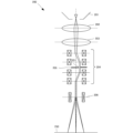
- FIG. 1 is a diagram showing a configuration of a three-dimensional additive manufacturing apparatus according to a first embodiment.
- FIG. FIG. 11 is a diagram showing a configuration of a three-dimensional additive manufacturing apparatus according to a second embodiment.
- FIG. 13 is a diagram showing another example of a three-dimensional additive manufacturing apparatus according to the second embodiment.
- FIG. 13 is a diagram showing yet another example of a three-dimensional additive manufacturing apparatus according to the second embodiment.
- the three-dimensional additive manufacturing apparatus 100 is an apparatus that performs additive manufacturing using an electron beam.
- the three-dimensional additive manufacturing apparatus 100 includes deflection units 101 to 104, a shielding plate 105, and a control unit 106.
- Deflection unit 101 changes the irradiation direction of the electron beam for melting.
- Deflection unit 102 changes the irradiation direction of the electron beam that has passed through deflection unit 101 to the vertical direction.
- Deflection unit 103 changes the irradiation direction of the electron beam that has passed through deflection unit 102.
- Deflection unit 104 changes the irradiation direction of the electron beam that has passed through deflection unit 103 to the vertical direction and irradiates the molded object.
- Shielding plate 105 is provided between deflection unit 102 and deflection unit 103, and has at least two apertures 151, 152 of different sizes for passing the electron beam.
- Control unit 106 controls the deflection direction in each of deflection units 101 to 104 to guide the electron beam to the apertures 151, 152 of different sizes of shielding plate 105.
- the above configuration makes it possible to protect the electron beam irradiation device 160 from metal vapor generated on the melting surface 150.
- the aperture diameter can be controlled according to the application.
- Fig. 2 is a diagram for explaining a schematic configuration of the three-dimensional additive manufacturing apparatus 200 according to this embodiment.
- the three-dimensional additive manufacturing system has the following characteristic structure.
- (1) A structure in which a four-stage deflection system is arranged between the electron gun for modeling and the objective lens or scanning coil.
- (2) A structure in which a shielding plate is arranged in the middle of the four-stage deflection system.
- (3) A structure in which a plurality of apertures are arranged in the shielding plate other than the center.
- (4) A structure in which the shielding plate itself is floating from GND so that the irradiation current can be measured.
- (5) A structure in which the shielding plate itself is made of a metal or the like that does not melt even if the temperature rises to 1000 degrees or more.
- FIG. 2 An example of a three-dimensional additive manufacturing system that realizes the above five structures is shown in FIG. 2.
- a four-stage deflection system is arranged in the modeling lens barrel of the electron beam additive manufacturing device.
- the lens barrel is composed of an electron gun for modeling 201, a pre-lens 202, an objective lens 203, and a scanning coil 206.
- a shielding plate 205 as shown in the figure is arranged in the center of the four-stage deflection system 204.
- a reflected electron image is taken during monitoring using the molten electron gun 201.
- An electron beam is generated by the electron gun 201 for modeling, collected by a pre-lens 202, and focused using an objective lens 203 before being irradiated onto the melt surface 250.
- Electron beam scanning for modeling is performed by a scanning coil 206. During pre-heating, a relatively large area is scanned at high speed with an irradiation current of several tens of mA to raise the temperature of the base plate 250. When melting and modeling, the current is reduced to several mA and the electron beam is applied only to the necessary areas. Furthermore, when observing the melting status, the current of the electron gun 201 is reduced to several tens of ⁇ A and a signal is detected by high-speed scanning.
- a shielding plate 205 is used to prevent vapor or gas from rising to the electron gun.
- the shielding plate 205 does not have an aperture at the center of the optical axis, but has an aperture 251 at a position offset from the optical axis.
- At least two apertures 251 are provided on the shielding plate 205, and each is used according to the purpose. For example, an aperture with a large diameter is used during preheating and shaping. An aperture with a smaller diameter is used when observing the melting state.
- a four-stage deflection system 204 is used to immediately deflect the electron beam against these apertures, and the shielding plate 205 is placed after the two-stage deflection of the four-stage deflection system. In other words, horizontal deflection is performed twice in two stages to return the beam to the original optical axis.
- the aperture provided in the shielding plate 205 is sized so as not to cause a loss of irradiation current.
- the shielding plate may further be positioned between the pre-lens and the objective lens (301) and/or below the scanning coil (302).
- the aperture may have two different diameters, one for preparatory heating and melting and shaping (large) and one for observation (small), or three different diameters, one for preparatory heating (maximum), one for melting and shaping (large), and one for observation (small).
- a material with a high melting point such as tungsten (molybdenum, tantalum, niobium, iridium, osmium, rhenium, hafnium, ruthenium, technetium, etc.) is used as the material for the shielding plate 205, the temperature rise is small even if the electron beam hits it directly, and the shielding plate 205 does not melt.
- the electron beam is directly hit on the shielding plate 205 without deflection using a four-stage deflection system.
- an electric circuit that floats it from GND is required, and it must be possible to change it instantly.
- the same aperture as during printing may be used.
- the irradiation current and probe diameter can be controlled according to the application.
- the four-stage deflection system is an electromagnetic deflection system, it is possible to control instantaneous switching of applications. Since a material that is difficult to melt can be used for the shielding plate, the irradiation current can be measured directly.
Landscapes
- Chemical & Material Sciences (AREA)
- Engineering & Computer Science (AREA)
- Analytical Chemistry (AREA)
- Automation & Control Theory (AREA)
- Manufacturing & Machinery (AREA)
- Materials Engineering (AREA)
- Powder Metallurgy (AREA)
Priority Applications (2)
| Application Number | Priority Date | Filing Date | Title |
|---|---|---|---|
| JP2025503251A JPWO2024180616A1 (https=) | 2023-02-27 | 2023-02-27 | |
| PCT/JP2023/007087 WO2024180616A1 (ja) | 2023-02-27 | 2023-02-27 | 3次元積層造形装置及び3次元積層造形方法 |
Applications Claiming Priority (1)
| Application Number | Priority Date | Filing Date | Title |
|---|---|---|---|
| PCT/JP2023/007087 WO2024180616A1 (ja) | 2023-02-27 | 2023-02-27 | 3次元積層造形装置及び3次元積層造形方法 |
Publications (1)
| Publication Number | Publication Date |
|---|---|
| WO2024180616A1 true WO2024180616A1 (ja) | 2024-09-06 |
Family
ID=92589316
Family Applications (1)
| Application Number | Title | Priority Date | Filing Date |
|---|---|---|---|
| PCT/JP2023/007087 Ceased WO2024180616A1 (ja) | 2023-02-27 | 2023-02-27 | 3次元積層造形装置及び3次元積層造形方法 |
Country Status (2)
| Country | Link |
|---|---|
| JP (1) | JPWO2024180616A1 (https=) |
| WO (1) | WO2024180616A1 (https=) |
Citations (3)
| Publication number | Priority date | Publication date | Assignee | Title |
|---|---|---|---|---|
| JP2013544030A (ja) * | 2010-11-13 | 2013-12-09 | マッパー・リソグラフィー・アイピー・ビー.ブイ. | アパーチャアレイ冷却部を備えた荷電粒子リソグラフィシステム |
| JP2019507236A (ja) * | 2015-12-10 | 2019-03-14 | ヴェロ・スリー・ディー・インコーポレイテッド | 性能向上した3次元印刷 |
| US20190310463A1 (en) * | 2016-10-27 | 2019-10-10 | Raylase Gmbh | Deflector |
Family Cites Families (4)
| Publication number | Priority date | Publication date | Assignee | Title |
|---|---|---|---|---|
| KR101480769B1 (ko) * | 2013-11-28 | 2015-01-22 | 한국생산기술연구원 | 입체 형상물 제조장치 및 입체 형상물 제조방법 |
| US11517975B2 (en) * | 2017-12-22 | 2022-12-06 | Arcam Ab | Enhanced electron beam generation |
| US11117195B2 (en) * | 2018-07-19 | 2021-09-14 | The University Of Liverpool | System and process for in-process electron beam profile and location analyses |
| JP7485309B2 (ja) * | 2019-01-29 | 2024-05-16 | フリーメルト エービー | 付加製造方法およびビームダンプを用いた装置 |
-
2023
- 2023-02-27 JP JP2025503251A patent/JPWO2024180616A1/ja active Pending
- 2023-02-27 WO PCT/JP2023/007087 patent/WO2024180616A1/ja not_active Ceased
Patent Citations (3)
| Publication number | Priority date | Publication date | Assignee | Title |
|---|---|---|---|---|
| JP2013544030A (ja) * | 2010-11-13 | 2013-12-09 | マッパー・リソグラフィー・アイピー・ビー.ブイ. | アパーチャアレイ冷却部を備えた荷電粒子リソグラフィシステム |
| JP2019507236A (ja) * | 2015-12-10 | 2019-03-14 | ヴェロ・スリー・ディー・インコーポレイテッド | 性能向上した3次元印刷 |
| US20190310463A1 (en) * | 2016-10-27 | 2019-10-10 | Raylase Gmbh | Deflector |
Also Published As
| Publication number | Publication date |
|---|---|
| JPWO2024180616A1 (https=) | 2024-09-06 |
Similar Documents
| Publication | Publication Date | Title |
|---|---|---|
| JP6989658B2 (ja) | 複数の荷電粒子ビームの装置 | |
| TWI650550B (zh) | 用於高產量電子束檢測(ebi)的多射束裝置 | |
| JP4215282B2 (ja) | 静電対物レンズ及び電気走査装置を装備したsem | |
| US20150213998A1 (en) | Charged particle beam device with dynamic focus and method of operating thereof | |
| KR20210076117A (ko) | 하전 입자 빔 디바이스, 필드 곡률 보정기, 및 하전 입자 빔 디바이스를 동작시키는 방법들 | |
| JP4171479B2 (ja) | 荷電粒子線応用装置及び荷電粒子線応用方法 | |
| CN108738363A (zh) | 多个带电粒子束的装置 | |
| KR20200119839A (ko) | 신호 전자들의 개선된 검출 성능을 갖는 멀티-빔 검사 장치 | |
| JP2024023374A (ja) | X線源の機械的アライメント | |
| IL267815B (en) | Reduced coulomb interactions in a multi-beam column | |
| TWI658487B (zh) | 多帶電粒子束裝置及用於觀測樣品表面之方法 | |
| JP2803831B2 (ja) | 走査電子顕微鏡 | |
| WO2024180616A1 (ja) | 3次元積層造形装置及び3次元積層造形方法 | |
| JP4357752B2 (ja) | 広域と局所的帯電を中和させる電子照射手段及び集束イオンビーム装置 | |
| US20080135786A1 (en) | Adjustable aperture element for particle beam device, method of operating and manufacturing thereof | |
| TWI729368B (zh) | 源轉換單元、多射束裝置及組態多射束裝置之方法 | |
| WO2002049066A1 (fr) | Microscope a faisceau de particules chargees, dispositif d'application de ce faisceau, procede d'utilisation du microscope en question, procede d'inspection via un tel faisceau, et microscope electronique | |
| JP4729403B2 (ja) | 電子ビーム露光装置 | |
| JP3687262B2 (ja) | 検査装置のレンズ電圧設定方法及び検査装置 | |
| KR100518812B1 (ko) | 주사 전자 현미경과 그 유사 장치에서 빈 필터에 의해발생되는 광행차의 감소 | |
| JP4558240B2 (ja) | 電子ビーム露光装置 | |
| JP4528589B2 (ja) | マスク検査装置、マスク検査方法及び電子ビーム露光装置 | |
| TWI787802B (zh) | 源轉換單元、多射束裝置及組態多射束裝置之方法 | |
| JP4450889B2 (ja) | 表面電位に基づく孤立パターン検出方法及びその電子顕微鏡 | |
| WO2024180614A1 (ja) | 3次元積層造形システムおよび3次元積層造形方法 |
Legal Events
| Date | Code | Title | Description |
|---|---|---|---|
| 121 | Ep: the epo has been informed by wipo that ep was designated in this application |
Ref document number: 23925174 Country of ref document: EP Kind code of ref document: A1 |
|
| WWE | Wipo information: entry into national phase |
Ref document number: 2025503251 Country of ref document: JP |
|
| NENP | Non-entry into the national phase |
Ref country code: DE |
|
| 122 | Ep: pct application non-entry in european phase |
Ref document number: 23925174 Country of ref document: EP Kind code of ref document: A1 |