WO2024177053A1 - 薄膜の製造方法及び薄膜形成用原料 - Google Patents
薄膜の製造方法及び薄膜形成用原料 Download PDFInfo
- Publication number
- WO2024177053A1 WO2024177053A1 PCT/JP2024/005979 JP2024005979W WO2024177053A1 WO 2024177053 A1 WO2024177053 A1 WO 2024177053A1 JP 2024005979 W JP2024005979 W JP 2024005979W WO 2024177053 A1 WO2024177053 A1 WO 2024177053A1
- Authority
- WO
- WIPO (PCT)
- Prior art keywords
- thin film
- general formula
- antimony
- bismuth
- metal thin
- Prior art date
- Legal status (The legal status is an assumption and is not a legal conclusion. Google has not performed a legal analysis and makes no representation as to the accuracy of the status listed.)
- Ceased
Links
Images


Classifications
-
- C—CHEMISTRY; METALLURGY
- C07—ORGANIC CHEMISTRY
- C07F—ACYCLIC, CARBOCYCLIC OR HETEROCYCLIC COMPOUNDS CONTAINING ELEMENTS OTHER THAN CARBON, HYDROGEN, HALOGEN, OXYGEN, NITROGEN, SULFUR, SELENIUM OR TELLURIUM
- C07F19/00—Metal compounds according to more than one of main groups C07F1/00 - C07F17/00
-
- C—CHEMISTRY; METALLURGY
- C23—COATING METALLIC MATERIAL; COATING MATERIAL WITH METALLIC MATERIAL; CHEMICAL SURFACE TREATMENT; DIFFUSION TREATMENT OF METALLIC MATERIAL; COATING BY VACUUM EVAPORATION, BY SPUTTERING, BY ION IMPLANTATION OR BY CHEMICAL VAPOUR DEPOSITION, IN GENERAL; INHIBITING CORROSION OF METALLIC MATERIAL OR INCRUSTATION IN GENERAL
- C23C—COATING METALLIC MATERIAL; COATING MATERIAL WITH METALLIC MATERIAL; SURFACE TREATMENT OF METALLIC MATERIAL BY DIFFUSION INTO THE SURFACE, BY CHEMICAL CONVERSION OR SUBSTITUTION; COATING BY VACUUM EVAPORATION, BY SPUTTERING, BY ION IMPLANTATION OR BY CHEMICAL VAPOUR DEPOSITION, IN GENERAL
- C23C16/00—Chemical coating by decomposition of gaseous compounds, without leaving reaction products of surface material in the coating, i.e. chemical vapour deposition [CVD] processes
- C23C16/44—Chemical coating by decomposition of gaseous compounds, without leaving reaction products of surface material in the coating, i.e. chemical vapour deposition [CVD] processes characterised by the method of coating
- C23C16/455—Chemical coating by decomposition of gaseous compounds, without leaving reaction products of surface material in the coating, i.e. chemical vapour deposition [CVD] processes characterised by the method of coating characterised by the method used for introducing gases into reaction chamber or for modifying gas flows in reaction chamber
- C23C16/45523—Pulsed gas flow or change of composition over time
- C23C16/45525—Atomic layer deposition [ALD]
- C23C16/45553—Atomic layer deposition [ALD] characterized by the use of precursors specially adapted for ALD
-
- C—CHEMISTRY; METALLURGY
- C07—ORGANIC CHEMISTRY
- C07F—ACYCLIC, CARBOCYCLIC OR HETEROCYCLIC COMPOUNDS CONTAINING ELEMENTS OTHER THAN CARBON, HYDROGEN, HALOGEN, OXYGEN, NITROGEN, SULFUR, SELENIUM OR TELLURIUM
- C07F9/00—Compounds containing elements of Groups 5 or 15 of the Periodic Table
- C07F9/90—Antimony compounds
-
- C—CHEMISTRY; METALLURGY
- C07—ORGANIC CHEMISTRY
- C07F—ACYCLIC, CARBOCYCLIC OR HETEROCYCLIC COMPOUNDS CONTAINING ELEMENTS OTHER THAN CARBON, HYDROGEN, HALOGEN, OXYGEN, NITROGEN, SULFUR, SELENIUM OR TELLURIUM
- C07F9/00—Compounds containing elements of Groups 5 or 15 of the Periodic Table
- C07F9/94—Bismuth compounds
-
- C—CHEMISTRY; METALLURGY
- C23—COATING METALLIC MATERIAL; COATING MATERIAL WITH METALLIC MATERIAL; CHEMICAL SURFACE TREATMENT; DIFFUSION TREATMENT OF METALLIC MATERIAL; COATING BY VACUUM EVAPORATION, BY SPUTTERING, BY ION IMPLANTATION OR BY CHEMICAL VAPOUR DEPOSITION, IN GENERAL; INHIBITING CORROSION OF METALLIC MATERIAL OR INCRUSTATION IN GENERAL
- C23C—COATING METALLIC MATERIAL; COATING MATERIAL WITH METALLIC MATERIAL; SURFACE TREATMENT OF METALLIC MATERIAL BY DIFFUSION INTO THE SURFACE, BY CHEMICAL CONVERSION OR SUBSTITUTION; COATING BY VACUUM EVAPORATION, BY SPUTTERING, BY ION IMPLANTATION OR BY CHEMICAL VAPOUR DEPOSITION, IN GENERAL
- C23C16/00—Chemical coating by decomposition of gaseous compounds, without leaving reaction products of surface material in the coating, i.e. chemical vapour deposition [CVD] processes
- C23C16/06—Chemical coating by decomposition of gaseous compounds, without leaving reaction products of surface material in the coating, i.e. chemical vapour deposition [CVD] processes characterised by the deposition of metallic material
- C23C16/18—Chemical coating by decomposition of gaseous compounds, without leaving reaction products of surface material in the coating, i.e. chemical vapour deposition [CVD] processes characterised by the deposition of metallic material from metallo-organic compounds
-
- C—CHEMISTRY; METALLURGY
- C23—COATING METALLIC MATERIAL; COATING MATERIAL WITH METALLIC MATERIAL; CHEMICAL SURFACE TREATMENT; DIFFUSION TREATMENT OF METALLIC MATERIAL; COATING BY VACUUM EVAPORATION, BY SPUTTERING, BY ION IMPLANTATION OR BY CHEMICAL VAPOUR DEPOSITION, IN GENERAL; INHIBITING CORROSION OF METALLIC MATERIAL OR INCRUSTATION IN GENERAL
- C23C—COATING METALLIC MATERIAL; COATING MATERIAL WITH METALLIC MATERIAL; SURFACE TREATMENT OF METALLIC MATERIAL BY DIFFUSION INTO THE SURFACE, BY CHEMICAL CONVERSION OR SUBSTITUTION; COATING BY VACUUM EVAPORATION, BY SPUTTERING, BY ION IMPLANTATION OR BY CHEMICAL VAPOUR DEPOSITION, IN GENERAL
- C23C16/00—Chemical coating by decomposition of gaseous compounds, without leaving reaction products of surface material in the coating, i.e. chemical vapour deposition [CVD] processes
- C23C16/22—Chemical coating by decomposition of gaseous compounds, without leaving reaction products of surface material in the coating, i.e. chemical vapour deposition [CVD] processes characterised by the deposition of inorganic material, other than metallic material
- C23C16/30—Deposition of compounds, mixtures or solid solutions, e.g. borides, carbides, nitrides
- C23C16/40—Oxides
-
- C—CHEMISTRY; METALLURGY
- C23—COATING METALLIC MATERIAL; COATING MATERIAL WITH METALLIC MATERIAL; CHEMICAL SURFACE TREATMENT; DIFFUSION TREATMENT OF METALLIC MATERIAL; COATING BY VACUUM EVAPORATION, BY SPUTTERING, BY ION IMPLANTATION OR BY CHEMICAL VAPOUR DEPOSITION, IN GENERAL; INHIBITING CORROSION OF METALLIC MATERIAL OR INCRUSTATION IN GENERAL
- C23C—COATING METALLIC MATERIAL; COATING MATERIAL WITH METALLIC MATERIAL; SURFACE TREATMENT OF METALLIC MATERIAL BY DIFFUSION INTO THE SURFACE, BY CHEMICAL CONVERSION OR SUBSTITUTION; COATING BY VACUUM EVAPORATION, BY SPUTTERING, BY ION IMPLANTATION OR BY CHEMICAL VAPOUR DEPOSITION, IN GENERAL
- C23C16/00—Chemical coating by decomposition of gaseous compounds, without leaving reaction products of surface material in the coating, i.e. chemical vapour deposition [CVD] processes
- C23C16/22—Chemical coating by decomposition of gaseous compounds, without leaving reaction products of surface material in the coating, i.e. chemical vapour deposition [CVD] processes characterised by the deposition of inorganic material, other than metallic material
- C23C16/30—Deposition of compounds, mixtures or solid solutions, e.g. borides, carbides, nitrides
- C23C16/40—Oxides
- C23C16/407—Oxides of zinc, germanium, cadmium, indium, tin, thallium or bismuth
Definitions
- the present invention relates to a method for producing a thin film and raw materials for forming a thin film.
- Patent Document 1 discloses a method for producing an antimony oxide thin film by atomic layer deposition.
- Patent Document 2 discloses a method for producing a germanium-antimony-tellurium film using antimony alkoxide and aminoantimony as one of multi-component films.
- Patent Document 3 discloses the formation of an antimony metal thin film using trichloroantimony and tris(triethylsilyl)antimony.
- Patent Documents 1 and 2 do not disclose a method for producing an antimony metal thin film.
- the method described in Patent Document 3 was not satisfactory in terms of the film formation rate or purity of the antimony metal thin film.
- antimony reacts well with compounds of different metals, it has a problem in that it has low reactivity with compounds of the same metal.
- bismuth atoms which are in the same group as antimony atoms, and no method for producing a thin film has been known that can form a high-purity bismuth metal thin film or antimony metal thin film with a high film formation rate, a uniform film thickness, and little residual carbon.
- the present invention therefore aims to provide a thin film manufacturing method and thin film forming raw material for use in the thin film manufacturing method, which can form a high-purity bismuth metal thin film or antimony metal thin film with a high film formation speed, uniform thickness, and little residual carbon.
- the present disclosure provides a method for producing a thin film, which forms a bismuth metal thin film or an antimony metal thin film using a compound represented by the following general formula (1) and a compound represented by the following general formula (2).
- M 1 represents trivalent bismuth or trivalent antimony.
- M2 represents trivalent bismuth or trivalent antimony
- L1 , L2 , and L3 each independently represent a halogen atom, an alkyl group having 1 to 10 carbon atoms, an alkoxy group having 1 to 10 carbon atoms, or a group represented by the following general formula (3), in which M1 and M2 are the same metal atom.
- R1 and R2 each independently represent a hydrogen atom, an alkyl group having 1 to 10 carbon atoms, or -SiR3R4R5 , R3 , R4 , and R5 each independently represent an alkyl group having 1 to 10 carbon atoms, and * represents the bonding position with M2 .
- the present disclosure provides a set of thin film forming raw materials, including a first thin film forming raw material containing a bismuth compound or antimony compound represented by the following general formula (1), and a second thin film forming raw material containing a bismuth compound or antimony compound represented by the following general formula (2).
- M 1 represents trivalent bismuth or trivalent antimony.
- M2 represents trivalent bismuth or trivalent antimony
- L1 , L2 , and L3 each independently represent a halogen atom, an alkyl group having 1 to 10 carbon atoms, an alkoxy group having 1 to 10 carbon atoms, or a group represented by the following general formula (3), in which M1 and M2 are the same metal atom.
- R1 and R2 each independently represent a hydrogen atom, an alkyl group having 1 to 10 carbon atoms, or -SiR3R4R5 , R3 , R4 , and R5 each independently represent an alkyl group having 1 to 10 carbon atoms, and * represents the bonding position with M2 .
- the present disclosure provides a method for producing a thin film that can form a high-purity bismuth metal thin film or antimony metal thin film with a fast film formation speed, uniform thickness, and little residual carbon, and a thin film forming raw material used in this method.
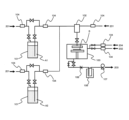
- FIG. 1 is a schematic diagram showing an example of an ALD apparatus used in a thin film manufacturing method according to the present invention.
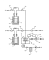
- FIG. 2 is a schematic diagram showing another example of an ALD apparatus used in the thin film manufacturing method according to the present invention.
- FIG. 2 is a schematic diagram showing yet another example of an ALD apparatus used in the thin film manufacturing method according to the present invention.
- FIG. 2 is a schematic diagram showing yet another example of an ALD apparatus used in the thin film manufacturing method according to the present invention.
- the method for producing a thin film according to the present disclosure will be described below. First, the raw materials for forming the thin film used in the method for producing a thin film according to the present disclosure will be described.
- A. Thin film forming raw materials As the thin film forming raw materials, a set of thin film forming raw materials is used, which includes a first thin film forming raw material containing a bismuth compound or an antimony compound represented by the general formula (1) above, and a second thin film forming raw material containing a bismuth compound or an antimony compound represented by the general formula (2) above. Each component constituting the first thin film forming material and the second thin film forming material will be described below.
- the first thin film forming raw material contains a bismuth compound or an antimony compound represented by the above general formula (1).
- M 1 represents trivalent bismuth or trivalent antimony.
- Examples of the compound represented by the above general formula (1) include the bismuth compound represented by the following No. 1 and the antimony compound represented by No. 2.
- the second thin film forming raw material contains a bismuth compound or an antimony compound represented by the above general formula (2).
- M2 represents trivalent bismuth or trivalent antimony, provided that M2 is the same metal atom as M1 in the above general formula (1).
- L 1 , L 2 and L 3 each represent a halogen atom, an alkyl group having 1 to 10 carbon atoms, an alkoxy group having 1 to 10 carbon atoms, or a group represented by the above general formula (3).
- Examples of the halogen atom represented by L 1 , L 2 and L 3 in the above general formula (2) include a fluorine atom, a chlorine atom, a bromine atom and an iodine atom.
- a fluorine atom, a chlorine atom, or a bromine atom is preferred, a fluorine atom or a chlorine atom is more preferred, and a chlorine atom is even more preferred. This is because the deposition rate is fast, the film thickness is uniform, and a high-purity metal thin film with little residual carbon can be formed.
- Examples of the alkyl group having 1 to 10 carbon atoms represented by L 1 , L 2 and L 3 in the above general formula (2) include a methyl group, an ethyl group, an n-propyl group, an isopropyl group, an n-butyl group, an isobutyl group, a sec-butyl group, a tert-butyl group, and the like.
- an alkyl group having 1 to 4 carbon atoms is preferred, an alkyl group having 1 to 3 carbon atoms is more preferred, and a methyl group or an ethyl group is even more preferred. This is because the deposition rate is fast, the film thickness is uniform, and a high-purity metal thin film with little residual carbon can be formed.
- Examples of the alkoxy group having 1 to 10 carbon atoms represented by L 1 , L 2 and L 3 in the above general formula (2) include a methoxy group, an ethoxy group, a propoxy group, a butoxy group, an isobutoxy group, a sec-butoxy group, a tert-butoxy group, an amyloxy group, an isoamyloxy group, a tert-amyloxy group, and a hexyloxy group.
- an alkoxy group having 1 to 7 carbon atoms is preferred, and an alkoxy group having 1 to 6 carbon atoms is more preferred. This is because the deposition rate is fast, the film thickness is uniform, and a high-purity metal thin film with little residual carbon can be formed.
- examples of the alkyl group having 1 to 10 carbon atoms represented by R1 and R2 include the same alkyl groups as those exemplified as the alkyl group having 1 to 10 carbon atoms represented by L1 , etc. in the general formula (2).
- R1 and R2 are preferably alkyl groups having 1 to 4 carbon atoms, more preferably alkyl groups having 1 to 3 carbon atoms, and even more preferably alkyl groups having 1 or 2 carbon atoms. This is because the deposition rate is fast, the film thickness is uniform, and a high-purity metal thin film with little residual carbon can be formed.
- the alkyl groups having 1 to 10 carbon atoms represented by R 3 , R 4 and R 5 include the same groups as the alkyl groups exemplified as the alkyl groups having 1 to 10 carbon atoms represented by L 1 , etc. in the above general formula (2).
- R3 , R4 , and R5 are preferably alkyl groups having 1 to 4 carbon atoms, more preferably alkyl groups having 1 to 3 carbon atoms, and even more preferably alkyl groups having 1 or 2 carbon atoms. This is because the deposition rate is fast, the film thickness is uniform, and a high-purity metal thin film with little residual carbon can be formed.
- L 1 , L 2 and L 3 may be different from each other or may be the same group, but it is preferable that they are all the same group. This is because the deposition rate is fast, the film thickness is uniform, and a high-purity metal thin film with little residual carbon can be formed.
- L1 , L2 , and L3 in the above general formula (2) are preferably a halogen atom, an alkyl group having 1 to 4 carbon atoms, an alkoxy group having 1 to 10 carbon atoms, or a group represented by the above general formula (3), more preferably a halogen atom, an alkoxy group having 1 to 10 carbon atoms, or a group represented by the above general formula (3), even more preferably an alkoxy group having 1 to 10 carbon atoms or a group represented by the above general formula (3), and even more preferably an alkoxy group having 4 to 6 carbon atoms, or a group represented by the above general formula (3).
- L1 , L2 , and L3 in the above general formula (2) are preferably a halogen atom, an alkyl group having 1 to 4 carbon atoms, an alkoxy group having 1 to 10 carbon atoms, or a group represented by the above general formula (3), more preferably a halogen atom, an alkoxy group having 1 to 10 carbon atoms, or a group represented by the above general formula (3), even more preferably a halogen atom, an alkoxy group having 1 to 3 carbon atoms, or a group represented by the above general formula (3), and even more preferably a chlorine atom, an alkoxy group having 1 to 3 carbon atoms, or a group represented by the above general formula (3).
- Preferred specific examples of the compound represented by the above general formula (2) include the following compounds No. 3 to No. 62. However, the present invention is not limited to these compounds.
- “Me” represents a methyl group
- “Et” represents an ethyl group
- “nPr” represents an n-propyl group
- "iPr” represents an isopropyl group
- "nBu” represents an n-butyl group
- sBu represents a sec-butyl group
- tBu represents a tert-butyl group.
- the molecular weight of the compound represented by the above general formula (2) is not limited, but is, for example, preferably 100 or more and 1,000 or less, more preferably 150 or more and 500 or less, even more preferably 200 or more and 490 or less, and most preferably 220 or more and 480 or less. This is because the deposition rate is fast, the film thickness is uniform, and a high-purity metal thin film with little residual carbon can be formed.
- the first thin film forming raw material and the second thin film forming raw material may contain the compound represented by the general formula (1) or the compound represented by the general formula (2), respectively, and the composition varies depending on the type of the target thin film.
- other components can be included in the thin film forming raw material as necessary. Examples of the other components include other precursors, nucleophilic reagents, etc.
- the other precursor may be a compound different from the compound represented by the general formula (1) and the compound represented by the general formula (2). From the viewpoint of forming a single metal thin film, it is preferable that the metal atom constituting the other precursor is the same as the metal atom in the compound represented by the general formula (1) and the compound represented by the general formula (2).
- the first and second thin film forming raw materials may each contain a well-known precursor as the other precursor.
- the other precursor include compounds of one or more compounds selected from compounds used as organic ligands such as alcohol compounds, glycol compounds, ⁇ -diketone compounds, cyclopentadiene compounds, and organic amine compounds, and a bismuth atom or an antimony atom.
- alcohol compounds that can be used as organic ligands for the other precursors include alkyl alcohols such as methanol, ethanol, propanol, isopropyl alcohol, butanol, sec-butyl alcohol, isobutyl alcohol, tert-butyl alcohol, pentyl alcohol, isopentyl alcohol, and tert-pentyl alcohol; 2-methoxyethanol, 2-ethoxyethanol, 2-butoxyethanol, 2-(2-methoxyethoxy)ethanol, 2-methoxy-1-methylethanol, 2-methoxy-1,1-dimethylethanol, 2-ethoxy-1,1-dimethylethanol, and 2-isopropoxy-1,1-dimethylethanol.
- alkyl alcohols such as methanol, ethanol, propanol, isopropyl alcohol, butanol, sec-butyl alcohol, isobutyl alcohol, tert-butyl alcohol, pentyl alcohol, isopentyl alcohol, and tert-pentyl alcohol
- ether alcohols such as 2-butoxy-1,1-dimethylethanol, 2-(2-methoxyethoxy)-1,1-dimethylethanol, 2-propoxy-1,1-diethylethanol, 2-sec-butoxy-1,1-diethylethanol, and 3-methoxy-1,1-dimethylpropanol; and dialkylamino alcohols such as dimethylaminoethanol, ethylmethylaminoethanol, diethylaminoethanol, dimethylamino-2-pentanol, ethylmethylamino-2-pentanol, dimethylamino-2-methyl-2-pentanol, ethylmethylamino-2-methyl-2-pentanol, and diethylamino-2-methyl-2-pentanol.
- dialkylamino alcohols such as dimethylaminoethanol, ethylmethylaminoethanol, diethylaminoethanol, dimethylamino-2-pentanol, e
- glycol compounds used as organic ligands for the other precursors include 1,2-ethanediol, 1,2-propanediol, 1,3-propanediol, 2,4-hexanediol, 2,2-dimethyl-1,3-propanediol, 2,2-diethyl-1,3-propanediol, 1,3-butanediol, 2,4-butanediol, 2,2-diethyl-1,3-butanediol, 2-ethyl-2-butyl-1,3-propanediol, 2,4-pentanediol, 2-methyl-1,3-propanediol, 2-methyl-2,4-pentanediol, 2,4-hexanediol, and 2,4-dimethyl-2,4-pentanediol.
- Beta-diketone compounds used as organic ligands for the other precursors above include, for example, acetylacetone, hexane-2,4-dione, 5-methylhexane-2,4-dione, heptane-2,4-dione, 2-methylheptane-3,5-dione, 5-methylheptane-2,4-dione, 6-methylheptane-2,4-dione, 2,2-dimethylheptane-3,5-dione, 2,6-dimethylheptane-3,5-dione, 2,2,6-trimethylheptane-3,5-dione, 2,2,6,6-tetramethylheptane-3,5-dione, octane-2,4-dione, 2,2,6-trimethyloctane-3,5-dione, 2,6-dimethyloctane-3,5-dione, 2,9-dimethylnonane-4,6-d
- Cyclopentadiene compounds used as organic ligands for the other precursors mentioned above include, for example, cyclopentadiene, methylcyclopentadiene, ethylcyclopentadiene, propylcyclopentadiene, isopropylcyclopentadiene, butylcyclopentadiene, sec-butylcyclopentadiene, isobutylcyclopentadiene, tert-butylcyclopentadiene, dimethylcyclopentadiene, tetramethylcyclopentadiene, pentamethylcyclopentadiene, etc.
- Organic amine compounds used as organic ligands for the other precursors include methylamine, ethylamine, propylamine, isopropylamine, butylamine, sec-butylamine, tert-butylamine, isobutylamine, dimethylamine, diethylamine, dipropylamine, diisopropylamine, ethylmethylamine, propylmethylamine, isopropylmethylamine, etc.
- the other precursors are known in the art, and their manufacturing methods are also known.
- the other precursor can be manufactured by reacting an inorganic salt or a hydrate thereof of the same metal atom as the metal atom of the compound represented by the general formula (1) with an alkali metal alkoxide of the alcohol compound.
- inorganic salts of metal atoms or hydrates thereof include metal halides and nitrates.
- alkali metal alkoxide include sodium alkoxide, lithium alkoxide, and potassium alkoxide.
- the other precursor when used as a raw material for forming a thin film, it is preferable that the other precursor is a compound whose thermal decomposition and/or oxidative decomposition behavior is similar to that of the compound represented by the general formula (1) or the compound represented by the general formula (2). This is because the deposition rate is fast, the film thickness is uniform, and a high-purity metal thin film with little residual carbon can be formed.
- the other precursor is a compound that exhibits similar thermal decomposition and/or oxidative decomposition behavior to the compound represented by the general formula (1) or the compound represented by the general formula (2), and that does not undergo deterioration due to chemical reaction or the like after being mixed with the compound represented by the general formula (1) or the compound represented by the general formula (2). This is because the deposition rate is fast, the film thickness is uniform, and a high-purity metal thin film with little residual carbon can be formed.
- the content of the above-mentioned other precursors is preferably 50 parts by mass or less, more preferably 30 parts by mass or less, even more preferably 10 parts by mass or less, even more preferably 5 parts by mass or less, and most preferably 0 parts by mass, i.e., the thin film forming raw material does not contain any other precursors, in 100 parts by mass of the thin film forming raw material. This is because the deposition rate is fast, the film thickness is uniform, and a high-purity metal thin film with little residual carbon can be formed.
- nucleophilic Reagent in the thin film manufacturing method of the present disclosure, can be contained in each of the first and second thin film forming raw materials in order to promote the reaction of the metal compound represented by the general formula (1) above, the metal compound represented by the general formula (2) above, or the other precursor with a reducing gas.
- nucleophilic reagents include, for example, ethylene glycol ethers such as glyme, diglyme, triglyme, and tetraglyme, crown ethers such as 18-crown-6, dicyclohexyl-18-crown-6, 24-crown-8, dicyclohexyl-24-crown-8, and dibenzo-24-crown-8, ethylenediamine, N,N'-tetramethylethylenediamine, diethylenetriamine, triethylenetetramine, tetraethylenepentamine, pentaethylenehexamine, 1,1,4,7,7-pentamethyldiethylenetriamine, and 1,1,4,7,10,10-hexamethyltriethylenetetramine.
- ethylene glycol ethers such as glyme, diglyme, triglyme, and tetraglyme
- crown ethers such as 18-crown-6, dicyclohexyl-18-crown-6, 24-c
- polyamines such as triethoxytriethyleneamine
- cyclic polyamines such as cyclam and cyclen
- heterocyclic compounds such as pyridine, pyrrolidine, piperidine, morpholine, N-methylpyrrolidine, N-methylpiperidine, N-methylmorpholine, tetrahydrofuran, tetrahydropyran, 1,4-dioxane, oxazole, thiazole, and oxathiolane
- ⁇ -ketoesters such as methyl acetoacetate, ethyl acetoacetate, and 2-methoxyethyl acetoacetate
- ⁇ -diketones such as acetylacetone, 2,4-hexanedione, 2,4-heptanedione, 3,5-heptanedione, and dipivaloylmethane.
- the content of the nucleophilic reagent is preferably 0.1 mol or more and 10 mol or less, and more preferably 1 mol or more and 4 mol or less, per 1 mol of the total amount of precursors in the first or second thin film forming raw materials. This is because it becomes easier to control the reaction between the compound represented by the general formula (1), the compound represented by the general formula (2), or the other precursor and the reducing gas described later.
- the total amount of the precursors refers to the total amount of the compound represented by general formula (1) or the compound represented by general formula (2) and the other precursors.
- the total amount of the precursors refers to the amount of the compound represented by general formula (1) or the compound represented by general formula (2).
- the thin film-forming raw material contains as few impurities as possible, such as impurity metal elements, impurity halogens, impurity organic matter, etc., except for the above-mentioned components constituting the thin film-forming raw material, i.e., the compound represented by the general formula (1), the compound represented by the general formula (2), the other precursors, and the nucleophilic reagent.
- the above-mentioned impurity metal element content may be a metal element different from the metal element constituting the compound represented by the above general formula (1) or the compound represented by the above general formula (2).
- the content of the impurity metal element in each of the first and second thin film forming raw materials is preferably 100 ppm or less, more preferably 10 ppm or less, and even more preferably 1 ppm or less, in terms of element content.
- the above-mentioned impurity halogen content includes halogen atoms different from the halogen atoms constituting the compound represented by the above general formula (2) and other precursors.
- the content of the impurity halogen content in the above-mentioned first and second thin film forming raw materials is preferably 100 ppm or less, more preferably 10 ppm or less, and even more preferably 1 ppm or less.
- the impurity organic matter may be an organic matter other than the compound represented by the general formula (1), the compound represented by the general formula (2), and the organic matter constituting the other precursors.
- the organic matter is composed of carbon and oxygen, excluding carbon monoxide and carbon dioxide, and examples of the organic matter include organic compounds other than the compound represented by the general formula (1), the compound represented by the general formula (2), and the other precursors.
- the total content of organic impurities in the first and second thin film forming materials is preferably 500 ppm or less, more preferably 50 ppm or less, and even more preferably 10 ppm or less.
- Moisture can cause particle generation in the first and second thin film forming raw materials and during thin film formation, so it is preferable to remove moisture from the compound represented by general formula (1), the compound represented by general formula (2), the other precursors, and the nucleophilic reagent before use in order to reduce the moisture content of each.
- the moisture content of the compound represented by general formula (1), the compound represented by general formula (2), the other precursors, and the nucleophilic reagent is preferably 10 ppm or less, and more preferably 1 ppm or less, respectively.
- the first and second thin film forming raw materials contain as few particles as possible in order to reduce or prevent particle contamination of the thin film to be formed.
- the number of particles larger than 0.3 ⁇ m is 100 or less per 1 ml of liquid phase, and it is even more preferable that the number of particles larger than 0.2 ⁇ m is 100 or less per 1 ml of liquid phase.
- the physical properties of the compound represented by the above general formula (1) or the compound represented by the above general formula (2) are also suitable for the CVD method, so the above thin film forming raw material is useful as a raw material for chemical vapor deposition.
- the compound represented by the above general formula (1) has a wide ALD window, so the above first thin film forming raw material is particularly suitable for the ALD method. Therefore, the above first thin film forming raw material is particularly useful as a thin film forming raw material for the ALD method.
- the first and second sets of thin film forming raw materials disclosed herein can form bismuth metal thin films or antimony metal thin films that have excellent electrical and optical properties, and these thin films are useful in various semiconductor devices, for example, as electrodes or contact layers.
- the set of thin film forming raw materials disclosed herein is particularly useful as thin film forming raw materials for forming bismuth metal thin films or antimony metal thin films.
- the present disclosure provides a method for producing a thin film, which comprises forming a bismuth metal thin film or an antimony metal thin film using the compound represented by the above general formula (1) and the compound represented by the above general formula (2).
- a method for producing a thin film according to the present disclosure it is particularly preferable to produce a thin film by an ALD method.
- the apparatus used in the thin film manufacturing method of the present disclosure may be a well-known ALD apparatus.
- the apparatus include an apparatus capable of bubbling and supplying a precursor as shown in Figures 1 and 3, and an apparatus having a vaporization chamber 102 as shown in Figures 2 and 4.
- Another example is an apparatus capable of performing plasma processing on a film deposition chamber 100 as shown in Figures 3 and 4.
- the apparatus is not limited to a single-wafer apparatus equipped with a film deposition chamber 100 as shown in Figures 1 to 4, but may also be an apparatus capable of simultaneously processing multiple wafers using a batch furnace. These may also be used as CVD apparatus.
- the method for producing a thin film according to the present disclosure by the ALD method includes, for example, a step of introducing a first source gas obtained by vaporizing a first source gas for forming a thin film, which contains a bismuth compound or an antimony compound represented by general formula (1), into a film formation chamber, and depositing the compound represented by general formula (1) in the first source gas on the surface of a substrate to form a precursor thin film; a step of introducing a second source gas obtained by vaporizing a second source gas for forming a thin film, which contains a bismuth compound or an antimony compound represented by general formula (2), into the film formation chamber, and reacting the precursor thin film with the second source gas to form a bismuth metal thin film or an antimony metal thin film; and a step of introducing at least one reducing gas selected from the group consisting of H 2 , NH 3 , H 2 plasma, and NH 3 plasma into the film formation chamber, and reacting the bismuth metal thin film or the antimony metal thin film with
- Precursor thin film formation step In this step, a first source gas obtained by vaporizing a first thin film forming raw material A1 containing a bismuth compound or an antimony compound represented by general formula (1) is introduced into the film formation chamber 100, and the bismuth compound or the antimony compound in the first source gas is deposited on the surface of the substrate S to form a precursor thin film.
- the substrate S is not particularly limited as long as it can support the precursor thin film.
- the substrate S may be any known substrate, and may be, for example, an organic compound or an inorganic compound.
- Examples of the material of the substrate S include silicon, ceramics such as silicon nitride, titanium nitride, tantalum nitride, titanium oxide, molybdenum oxide, zirconium oxide, hafnium oxide, and lanthanum oxide, glass, and metals such as metallic cobalt, metallic molybdenum, molybdenum sulfide, molybdenum selenide, tungsten sulfide, and tungsten selenide.
- Examples of the shape of the substrate include plate-like, spherical, fibrous, scaly, flat or disc-like, fibrous, cylindrical, prismatic, cylindrical, spiral, spherical, ring-like, and three-dimensional structures such as trench structures.
- the thickness of the substrate S is not particularly limited in the present disclosure, but is preferably, for example, 1 ⁇ or more and 1 ⁇ m or less, and more preferably 1 ⁇ or more and 50 nm or less. This is because the deposition rate is fast, the film thickness is uniform, and a high-purity metal thin film with little residual carbon can be formed.
- the surface of the substrate S refers not only to the surface of a substrate S such as silicon, but also to the surface of a bismuth metal thin film or an antimony metal thin film formed by the cycle of a thin film manufacturing method described later.
- the first source gas is obtained by vaporizing a first thin film-forming raw material A1 containing a bismuth compound or an antimony compound represented by the general formula (1) above.
- the first source gas can be obtained, for example, by heating and/or reducing the pressure of the first thin film-forming source material A1 containing the bismuth compound or antimony compound represented by the general formula (1) above.
- Examples of a method for heating the first thin film forming raw material A1 include a method for heating the thin film forming raw material in the raw material container 101 in the ALD apparatus shown in FIG. 1 or FIG. 3, and a method for heating the thin film forming raw material in the vaporization chamber 102 in the ALD apparatus shown in FIG. 2 or FIG. 4.
- the temperature range for heating the first thin film forming raw material A1 is, for example, preferably 300° C. or lower, more preferably 20° C. or higher and 250° C. or lower, and further preferably 30° C. or higher and 200° C. or lower. This is because the deposition rate is fast, the film thickness is uniform, and a high-purity metal thin film with little residual carbon can be formed.
- Examples of a method for reducing the pressure of the first thin film forming raw material A1 include a method for reducing the pressure of the thin film forming raw material in the raw material container 101 of the ALD apparatus shown in FIG. 1 or FIG. 3, or a method for reducing the pressure of the thin film forming raw material in the vaporization chamber 102 of the ALD apparatus shown in FIG. 2 or FIG. 4.
- the reduced pressure (vacuum degree) conditions are, for example, preferably 1 Pa or more and 10,000 Pa or less, more preferably 10 Pa or more and 5,000 Pa or less, and even more preferably 20 Pa or more and 1,000 Pa or less. This is because the deposition rate is fast, the film thickness is uniform, and a high-purity metal thin film with little residual carbon can be formed.
- the first source gas may be introduced into the deposition chamber 100 by a gas transport method, a liquid transport method, or the like.
- a gas transport method as shown in Figures 1 and 3
- the first thin film formation raw material A1 is heated and/or vaporized in a raw material container 101 to form a first raw material gas
- the first raw material gas is introduced into a film formation chamber 100 together with a carrier gas 201 such as argon, nitrogen, helium, etc. as necessary.
- the first thin film forming raw material is transported in a liquid or solution state to a vaporization chamber 102, and in the vaporization chamber 102, the first thin film forming raw material A1 is heated and/or depressurized to form a first raw material gas, and the first raw material gas is introduced into the film formation chamber 100 together with a carrier gas 201 such as argon, nitrogen, helium, etc. as necessary.
- a carrier gas 201 such as argon, nitrogen, helium, etc.
- the first raw material gas can be introduced into the film forming chamber 100 by using, for example, a single source method.
- the bismuth compound or antimony compound in the first source gas introduced into the film formation chamber 100 is deposited on the surface of the substrate S previously placed in the film formation chamber 100 to form a precursor thin film.
- “deposition” refers to a concept including chemical adsorption of a compound on the surface of the substrate S.
- the first raw material gas is preferably heated at, for example, 25°C or higher and 270°C or lower, more preferably 25°C or higher and 250°C or lower, and particularly preferably 25°C or higher and 230°C or lower. This is because the deposition rate is fast, the film thickness is uniform, and a high-purity metal thin film with little residual carbon can be formed.
- the first raw material gas is heated, for example, preferably at 25°C or higher and 400°C or lower, more preferably at 25°C or higher and 300°C or lower, even more preferably at 25°C or higher and 250°C or lower, even more preferably at 25°C or higher and 200°C or lower, and most preferably at 25°C or higher and 150°C or lower. This is because the deposition rate is fast, the film thickness is uniform, and a high-purity metal thin film with little residual carbon can be formed.
- the heating of the first raw material gas is preferably carried out in an oxygen-free atmosphere, particularly in an inert gas atmosphere such as nitrogen gas or argon gas, and particularly in an inert gas atmosphere.
- an inert gas atmosphere such as nitrogen gas or argon gas
- the heating reaction may be carried out under any of increased pressure, reduced pressure, normal pressure and atmospheric pressure, but in this step, it is preferably carried out under reduced pressure (20 Pa or more and 1,000 Pa or less). This is because the deposition rate is fast, the film thickness is uniform, and a high-purity metal thin film with little residual carbon can be formed.
- the second source gas is obtained by vaporizing the second thin film formation source A2 containing the bismuth compound or antimony compound represented by the general formula (2) above.
- the method for obtaining the second raw material gas can be the same as that described in the section "B1(2) Introduction of the first raw material gas” except that the compound represented by the general formula (1) is replaced with the compound represented by the general formula (2), and therefore the description thereof will be omitted here.
- the compound represented by the general formula (2) may react and decompose when it comes into contact with the compound represented by the general formula (1), it is preferable to prevent the first thin film forming raw material A1 containing the compound represented by the general formula (1) from coming into contact with the second thin film forming raw material A2 containing the compound represented by the general formula (2) by, for example, separating the supply lines for the thin film forming raw materials from the raw material container 101 to the film formation chamber 100 in the ALD apparatus shown in Figures 1 to 4.
- the second source gas introduced into the film formation chamber 100 as described above is reacted with the precursor thin film to form a bismuth metal thin film or an antimony metal thin film.
- the heating of the second source gas and the pressure inside the deposition chamber 100 during heating can be performed under the same conditions as those for heating the first source gas in the above-mentioned section “B1(3) Formation of precursor thin film”.
- the reaction is preferably carried out at 20° C. or higher and 90° C. or lower, more preferably at 20° C. or higher and 75° C. or lower, and even more preferably at 20° C. or higher and 60° C. or lower.
- the second source gas is heated to promote a reaction between the bismuth compound or antimony compound represented by general formula (1) in the precursor thin film and the bismuth compound or antimony compound represented by general formula (2) contained in the second source gas, thereby forming a bismuth metal thin film or an antimony metal thin film on the substrate.
- the bismuth compound or antimony compound represented by general formula (1) in the precursor thin film
- the bismuth compound or antimony compound represented by general formula (2) contained in the second source gas thereby forming a bismuth metal thin film or an antimony metal thin film on the substrate.
- Bi( SiMe3 ) 3 compound No. 1
- Bi( NMe2 ) 3 compound No. 27
- the first source gas is first introduced into the deposition chamber 100, a precursor thin film is formed, and then the second source gas is introduced.
- a process may also be performed in which the second source gas obtained by vaporizing the second thin film forming source A2 is first introduced into the deposition chamber 100, a compound represented by general formula (2) is deposited on the surface of the substrate S to form a precursor thin film, and then the first source gas obtained by vaporizing the first thin film forming source A1 containing the compound represented by general formula (1) is introduced into the deposition chamber 100, and the precursor thin film and the first source gas are reacted to form a bismuth metal thin film or an antimony metal thin film.
- metal thin film purification step In this step, at least one reducing gas 202 selected from the group consisting of H2 , NH3 , H2 plasma, and NH3 plasma is introduced into the deposition chamber 100 and reacted with the bismuth metal thin film or the antimony metal thin film to purify the bismuth metal thin film or the antimony metal thin film.
- the purification step here refers to a step of increasing the content of bismuth atoms or antimony atoms contained in 100 parts by mass of the bismuth metal thin film or antimony metal thin film obtained in the previous step to close to 100 parts by mass.
- the reducing gas 202 may be one or a combination of two or more selected from the group consisting of H 2 , NH 3 , H 2 plasma, and NH 3 plasma.
- the H2 preferably has an impurity content of 10 ppm or less, more preferably 1 ppm or less, and particularly preferably 100 ppb or less. This is because the deposition rate is fast, the film thickness is uniform, and a high-purity metal thin film with little residual carbon can be formed.
- the impurities include H 2 O, O 2 , CO 2 , metals other than M 1 in the general formula (1) above, and NMHC.
- the NH3 has preferably 10 ppm or less of the above impurities, more preferably 1 ppm or less, and particularly preferably 100 ppb or less. This is because the deposition rate is fast, the film thickness is uniform, and a high-purity metal thin film with little residual carbon can be formed.
- H2 plasma H2 plasma refers to a plasma having H radicals.
- H2 plasma can be produced by converting H2 into plasma using, for example, a direct current (DC) current, an alternating current (RF) current, microwaves, etc.
- DC direct current
- RF alternating current
- an RF matching system 106 connected to a radio frequency (RF) power source 105 is installed in a film formation chamber 100, and plasma can be generated in the film formation chamber 100.
- RF radio frequency
- NH3 plasma refers to NH3 having radicals.
- NH3 plasma can be produced by directly reacting H2 and N2 using, for example, direct current (DC) current, alternating current (RF) current, microwaves, etc.
- DC direct current
- RF alternating current
- an RF matching system 106 connected to a radio frequency (RF) power source 105 is installed in a film formation chamber 100, and plasma can be generated in the film formation chamber 100.
- the thin film production method of the present disclosure may contain other gases as the reducing gas in addition to H 2 , NH 3 , H 2 plasma, and NH 3 plasma.
- the other gases include organic amine compounds such as monoalkylamines, dialkylamines, trialkylamines, and alkylenediamines; nitriding gases obtained by vaporizing hydrazine or the like; sulfurizing gases such as dialkyl sulfides such as sulfur, hydrogen sulfide, dimethyl sulfide, diethyl sulfide, and diisopropyl sulfide; and inert gases such as argon and nitrogen.
- the other gases may be used in combination of two or more.
- the content of other gases in the reducing gas is preferably 50 vol. % or less, more preferably 10 vol. % or less, and particularly preferably 5 vol. % or less.
- the reducing gas 202 preferably contains only a gas selected from the group consisting of H 2 , NH 3 , H 2 plasma, and NH 3 plasma, and it is more preferable to use only a gas selected from the group consisting of H 2 and H 2 plasma, and it is even more preferable to use only H 2 from the viewpoints of high reactivity and suppression of damage to the underlying layer. This is because the deposition rate is fast, the film thickness is uniform, and a high-purity metal thin film with little residual carbon can be formed.
- the method of introducing at least one selected from the group consisting of H2 , NH3 , H2 plasma, and NH3 plasma into the film formation chamber 100 can be performed in the same manner as the first source gas or the second source gas described above.
- H 2 plasma or NH 3 plasma is introduced, for example, H 2 and NH 3 may be introduced into the film formation chamber 100 of FIG. 3 or FIG. 4, and then a voltage may be applied to generate plasma.
- the reaction between the metal thin film and the reducing gas 202 is carried out by heating the metal thin film and/or the reducing gas 202, and it is preferable that the heating in this process is carried out at the same temperature as in the precursor formation process and the metal thin film formation process. This is because the above-mentioned metal thin film with high purity can be efficiently produced.
- the heating is preferably carried out at, for example, 25° C. or higher and 270° C. or lower, more preferably 25° C. or higher and 250° C. or lower, and particularly preferably 25° C. or higher and 230° C. or lower. This is because the above-mentioned metal thin film with high purity can be efficiently produced.
- the heating is preferably carried out at a temperature of from 25° C. to 400° C., more preferably from 25° C. to 300° C., even more preferably from 25° C. to 250° C., even more preferably from 25° C. to 200° C., and most preferably from 25° C. to 150° C. This is because the above-mentioned metal thin film with high purity can be efficiently produced.
- the system pressure is not particularly limited, but is preferably 1 Pa or more and 10,000 Pa or less, and more preferably 10 Pa or more and 1,000 Pa or less from the viewpoint of easily and efficiently producing the above-mentioned high-purity metal thin film.
- the method for producing a thin film according to the present disclosure may include other steps such as exhaust steps 1 to 3, a plasma treatment step, an annealing treatment step, and a reflow step.
- Exhaust process 1 This step is a step of exhausting (203) the unreacted first source gas that has not been involved in the formation of the precursor thin film from the film formation chamber 100 after the precursor thin film formation step. In this step, it is ideal that the unreacted first source gas is completely exhausted from inside the film formation chamber 100, but it is not always necessary to exhaust it completely.
- Examples of the exhaust method include a method of purging the inside of the deposition chamber 100 with an inert gas (purge gas 204) such as helium, nitrogen, or argon, a method of exhausting the inside of the system by reducing the pressure while controlling the degree of pressure reduction using a vacuum pump 107 and an automatic pressure controller 108, and a combination of these methods.
- the degree of reduction in pressure is, for example, preferably 0.01 Pa or more and 300 Pa or less, more preferably 0.05 Pa or more and 200 Pa or less, and particularly preferably 0.1 Pa or more and 100 Pa or less. This is because the first source gas can be exhausted sufficiently, the deposition rate is fast, the thickness is uniform, and a high-purity thin metal film with little residual carbon can be formed.
- Exhaust process 2 This process is a process of exhausting unreacted second source gas that was not involved in the formation of the metal thin film and by-product gas produced by the reaction of the precursor thin film with the second source gas from the film formation chamber 100 after the above-mentioned metal thin film formation process. In this step, it is ideal that the unreacted second source gas and by-product gas are completely exhausted from the film formation chamber 100, but it is not always necessary to completely exhaust them.
- the evacuation method and the degree of pressure reduction can be the same as those in the evacuation step 1.
- Exhaust process 3 This step is a step of exhausting unreacted reducing gas and by-product gases generated during the reduction of the metal thin film from within the film formation chamber after the metal thin film purification step. In this step, it is ideal that the unreacted reducing gas 202 and by-product gases are completely exhausted from the film formation chamber, but it is not always necessary to completely exhaust them.
- the evacuation method and the degree of pressure reduction can be the same as those in the evacuation step 1.
- the thin film manufacturing method of the present disclosure may include a plasma treatment step of applying a voltage to the first source gas or the second source gas to convert it into plasma in order to promote the formation of the precursor thin film and the formation of the metal thin film.
- a plasma treatment step of applying a voltage to the first source gas or the second source gas to convert it into plasma in order to promote the formation of the precursor thin film and the formation of the metal thin film.
- an RF matching system 106 connected to a radio frequency (RF) power supply 105 is installed in the film formation chamber 100, and the first and second source gases can be turned into plasma in the film formation chamber 100.
- RF radio frequency
- the power when applying the voltage is, for example, preferably 10 W or more and 1,500 W or less, more preferably 30 W or more and 1,000 W or less, and even more preferably 50 W or more and 600 W or less.
- the annealing step may be a step of annealing the metal thin film after purifying the metal thin film in order to improve the electrical characteristics of the metal layer.
- the metal thin film can be annealed in an inert atmosphere or a reducing atmosphere.
- the temperature in the annealing treatment is preferably 100° C. or higher and 270° C. or lower, more preferably 150° C. or higher and 260° C. or lower, and particularly preferably 200° C. or higher and 250° C. or lower.
- the temperature in the annealing treatment is preferably 100° C.
- the reflow step may be a step of heating the thin metal film after the thin metal film is formed in order to fill in any steps in the thin metal film.
- the temperature in the reflow step is, for example, preferably 200° C. or higher and 600° C. or lower, more preferably 230° C. or higher and 550° C. or lower, and particularly preferably 250° C. or higher and 500° C. or lower. This is because the deposition rate is fast, the film thickness is uniform, and a high-purity metal thin film with little residual carbon can be formed.
- a precursor thin film formation step, an exhaust step 1, a metal thin film formation step, an exhaust step 2, a purification step, and an exhaust step 3 are sequentially performed, and the formation of the above-mentioned thin film by a series of operations is regarded as one cycle.
- a thin film of a metal layer having a required thickness is obtained, a thin film of a metal layer having a desired thickness can be produced. That is, the thickness of the thin film formed can be controlled by the number of cycles.
- the above cycle may be performed only once to form one layer of a metal thin film, or may be performed twice or more to produce a metal thin film of a desired thickness.
- the thickness of the thin film obtained per cycle is preferably 0.1 ⁇ to 1.0 nm, more preferably 0.3 ⁇ to 0.5 nm, and particularly preferably 0.5 ⁇ to 0.1 nm. This is because a metal thin film of uniform thickness can be easily obtained.
- B6. Thin Film Manufacturing Method Other Than ALD Method a method for manufacturing a bismuth metal thin film or an antimony metal thin film by ALD has been described, but the method for manufacturing a thin film of the present disclosure is not limited to the above, and a thin film may be manufactured by, for example, a CVD method.
- the thin film manufacturing method of the present disclosure uses a CVD method to manufacture a thin film, the first source gas and the second source gas may be introduced into the film formation chamber 100 at the same time.
- the bismuth metal thin film or antimony metal thin film produced by the method for producing a thin film according to the present disclosure contains 90 parts by mass or more of bismuth atoms or antimony atoms per 100 parts by mass of the thin film.
- the content of bismuth atoms or antimony atoms in 100 parts by mass of the thin film is preferably 96 parts by mass or more, more preferably 97 parts by mass or more, even more preferably 98 parts by mass or more, and even more preferably 99 parts by mass or more. This is because bismuth metal thin films and antimony metal thin films exhibit excellent electrical properties and can be used in a variety of semiconductor devices.
- the amount of residual carbon and oxygen in the thin film is preferably small, and is preferably 5 atom % or less, more preferably 3 atom % or less, and even more preferably 1 atom % or less. This is because it is possible to obtain thin films that exhibit excellent electrical properties and that can be used in a variety of semiconductor devices.
- the semiconductor device examples include a field effect transistor (FET), a nanosheet transistor, a nanowire transistor, and a complementary field effect (FET) transistor.
- the semiconductor device is preferably a FET having a semiconductor layer made of a transition metal dichalcogenide such as MoS 2 , MoSe 2 , WS 2 , or WSe 2.
- the thin film forming material of the present disclosure is preferably formed as a contact or metal thin film on the upper or lower part of the transition metal dichalcogenide semiconductor layer. This is because the bismuth metal thin films and antimony metal thin films produced by the thin film production method of the present disclosure have excellent electrical properties.
- the semiconductor device may further include other layers (for example, an insulating layer, a conductor layer, a semiconductor layer, a buffer layer, or other intermediate layers).
- Example 1 Using the bismuth compound No. 1 (first thin film forming raw material A1) as the compound represented by general formula (1) and the bismuth compound No. 23 (second thin film forming raw material A2) as the compound represented by general formula (2), a thin film was produced on a silicon substrate as a base S under the following conditions using the ALD apparatus shown in FIG. The composition of the obtained thin film was analyzed by X-ray diffraction and X-ray photoelectron spectroscopy. The thin film was found to be a bismuth metal thin film, with a residual carbon content of 1.0 atom % and a residual oxygen content of 1.0 atom %.
- the thin film formed on the substrate was a smooth film with a thickness of 600 ⁇ , and the film thickness obtained per cycle was 0.6 ⁇ .
- the film thickness obtained per cycle is 0.5 ⁇ or more, it can be said that the film formation speed is fast.
- the X-ray reflectometry an apparatus manufactured by Rigaku Corporation was used, and for the spectroscopic ellipsometry, an apparatus manufactured by J. A. Woollam Company was used.
- Step 1 The vapor of the first thin film forming raw material A1 (first raw material gas) vaporized under conditions of a heating temperature of the raw material container 101 of 80° C. and an internal pressure of the raw material container 101 of 100 Pa is introduced into the film formation chamber 100, and the bismuth compound in the first raw material gas is adsorbed onto the surface of the substrate S at a system pressure of 100 Pa for 15 seconds to form a precursor thin film.
- Step 2 The unadsorbed first source gas is purged with argon for 10 seconds to be exhausted from the system.
- Step 3 The vapor of the second thin film forming raw material A2 (second raw material gas) vaporized under conditions of a heating temperature of 100° C. of the raw material container 101 and an internal pressure of the raw material container 101 of 100 Pa is introduced into the film formation chamber 100 and reacted with the precursor thin film formed in step 1 at a system pressure of 100 Pa for 15 seconds.
- Step 4 The unreacted second raw material gas and by-product gases are discharged from the system by purging with argon for 10 seconds.
- Step 5 A reducing gas 202 is introduced into the film-forming chamber 100 and reacted with the bismuth metal thin film formed in step 3 at a system pressure of 100 Pa for 15 seconds to highly purify the bismuth metal thin film.
- Step 6 Unreacted reducing gas 202 and by-product gases are exhausted from the system by argon purging for 10 seconds.
- Example 2 A thin film was produced in the same manner as in Example 1, except that antimony compound No. 2 (first thin film forming raw material A1) was used as the compound represented by general formula (1), antimony compound No. 46 (second thin film forming raw material A2) was used as the compound represented by general formula (2), the ALD apparatus shown in FIG. 1 was used, and the heating temperature of the raw material container 101 in step 3 was changed to 45° C.
- the composition of the obtained thin film was analyzed by X-ray diffraction and X-ray photoelectron spectroscopy. The thin film was found to be an antimony metal thin film, with a residual carbon content of 1.0 atom % and a residual oxygen content of 1.0 atom %.
- the thin film formed on the substrate S was a smooth film with a thickness of 500 ⁇ , and the film thickness obtained per cycle was 0.5 ⁇ .
- Comparative Example 1 A thin film was produced in the same manner as in Example 1, except that the bismuth compound No. 1 was used as the compound represented by general formula (1), triphenylbismuth was used as a comparative compound for the compound represented by general formula (2), the ALD apparatus shown in FIG. 1 was used, and the heating temperature of the source container 101 in step 3 was changed to 180° C. However, bismuth metal was not produced, and a bismuth metal thin film could not be formed.
- Comparative Example 2 A thin film was produced in the same manner as in Example 1, except that antimony compound No. 2 was used as the compound represented by general formula (1), triphenylantimony was used as a comparative compound for the compound represented by general formula (2), and the ALD apparatus shown in Figure 1 was used, and the reaction temperature (substrate temperature) was changed to 220°C, and the heating temperature of the source container 101 in step 3 was changed to 160°C.
- antimony metal was not produced, and an antimony metal thin film could not be formed.
- the thin film manufacturing method of the present invention can form high-purity metal thin films with a fast film formation rate, uniform thickness, and little residual carbon.
- the bismuth metal thin film or antimony metal thin film manufactured by the thin film manufacturing method of the present invention has a significantly thicker film thickness per cycle, suggesting that the thin film manufacturing method of the present invention can achieve high productivity.
- Film-forming chamber 101 Source container 102: Vaporization chamber 103: Heater 104: Mass flow controller (MFC) 105 Radio Frequency (RF) power source 106 RF matching system 107 Vacuum pump 108 Automatic pressure controller 109 Cold trap 201 Carrier gas 202 Reducing gas 203 Exhaust 204 Purge gas A1 First thin film forming material A2 Second thin film forming material S Substrate
Landscapes
- Chemical & Material Sciences (AREA)
- Organic Chemistry (AREA)
- General Chemical & Material Sciences (AREA)
- Chemical Kinetics & Catalysis (AREA)
- Engineering & Computer Science (AREA)
- Materials Engineering (AREA)
- Mechanical Engineering (AREA)
- Metallurgy (AREA)
- Inorganic Chemistry (AREA)
- Chemical Vapour Deposition (AREA)
- Plural Heterocyclic Compounds (AREA)
Priority Applications (4)
| Application Number | Priority Date | Filing Date | Title |
|---|---|---|---|
| IL322598A IL322598A (en) | 2023-02-24 | 2024-02-20 | Method for producing a thin layer and raw material for forming a thin layer |
| JP2025502733A JPWO2024177053A1 (https=) | 2023-02-24 | 2024-02-20 | |
| EP24760351.7A EP4671410A1 (en) | 2023-02-24 | 2024-02-20 | THIN FILM MANUFACTURING PROCESS AND THIN FILM FORMING MATERIAL |
| KR1020257030928A KR20250154424A (ko) | 2023-02-24 | 2024-02-20 | 박막의 제조 방법 및 박막 형성용 원료 |
Applications Claiming Priority (2)
| Application Number | Priority Date | Filing Date | Title |
|---|---|---|---|
| JP2023027200 | 2023-02-24 | ||
| JP2023-027200 | 2023-02-24 |
Publications (1)
| Publication Number | Publication Date |
|---|---|
| WO2024177053A1 true WO2024177053A1 (ja) | 2024-08-29 |
Family
ID=92501383
Family Applications (1)
| Application Number | Title | Priority Date | Filing Date |
|---|---|---|---|
| PCT/JP2024/005979 Ceased WO2024177053A1 (ja) | 2023-02-24 | 2024-02-20 | 薄膜の製造方法及び薄膜形成用原料 |
Country Status (6)
| Country | Link |
|---|---|
| EP (1) | EP4671410A1 (https=) |
| JP (1) | JPWO2024177053A1 (https=) |
| KR (1) | KR20250154424A (https=) |
| IL (1) | IL322598A (https=) |
| TW (1) | TW202440604A (https=) |
| WO (1) | WO2024177053A1 (https=) |
Citations (3)
| Publication number | Priority date | Publication date | Assignee | Title |
|---|---|---|---|---|
| JP2013508555A (ja) | 2009-10-26 | 2013-03-07 | アーエスエム インターナショナル エヌフェー | Va族元素を含む薄膜のaldのための前駆体の合成及び使用 |
| JP2013084959A (ja) | 2011-10-12 | 2013-05-09 | Asm Internatl Nv | 酸化アンチモン膜の原子層堆積 |
| JP2015007279A (ja) | 2013-04-11 | 2015-01-15 | エア プロダクツ アンド ケミカルズ インコーポレイテッドAir Products And Chemicals Incorporated | 多成分膜の製造方法 |
-
2024
- 2024-02-20 JP JP2025502733A patent/JPWO2024177053A1/ja active Pending
- 2024-02-20 IL IL322598A patent/IL322598A/en unknown
- 2024-02-20 WO PCT/JP2024/005979 patent/WO2024177053A1/ja not_active Ceased
- 2024-02-20 EP EP24760351.7A patent/EP4671410A1/en active Pending
- 2024-02-20 KR KR1020257030928A patent/KR20250154424A/ko active Pending
- 2024-02-22 TW TW113106326A patent/TW202440604A/zh unknown
Patent Citations (4)
| Publication number | Priority date | Publication date | Assignee | Title |
|---|---|---|---|---|
| JP2013508555A (ja) | 2009-10-26 | 2013-03-07 | アーエスエム インターナショナル エヌフェー | Va族元素を含む薄膜のaldのための前駆体の合成及び使用 |
| JP5731519B2 (ja) * | 2009-10-26 | 2015-06-10 | エーエスエム インターナショナル エヌ.ヴェー.Asm International N.V. | Va族元素を含む薄膜のaldのための前駆体の合成及び使用 |
| JP2013084959A (ja) | 2011-10-12 | 2013-05-09 | Asm Internatl Nv | 酸化アンチモン膜の原子層堆積 |
| JP2015007279A (ja) | 2013-04-11 | 2015-01-15 | エア プロダクツ アンド ケミカルズ インコーポレイテッドAir Products And Chemicals Incorporated | 多成分膜の製造方法 |
Non-Patent Citations (2)
| Title |
|---|
| AL HARERI MAJEDA, EMSLIE DAVID J. H.: "Room-Temperature Atomic Layer Deposition of Elemental Antimony", CHEMISTRY OF MATERIALS, vol. 34, no. 5, 8 March 2022 (2022-03-08), US , pages 2400 - 2409, XP093203018, ISSN: 0897-4756, DOI: 10.1021/acs.chemmater.1c04411 * |
| See also references of EP4671410A1 |
Also Published As
| Publication number | Publication date |
|---|---|
| TW202440604A (zh) | 2024-10-16 |
| EP4671410A1 (en) | 2025-12-31 |
| KR20250154424A (ko) | 2025-10-28 |
| IL322598A (en) | 2025-10-01 |
| JPWO2024177053A1 (https=) | 2024-08-29 |
Similar Documents
| Publication | Publication Date | Title |
|---|---|---|
| JP5843318B2 (ja) | Ald法用窒化アルミニウム系薄膜形成用原料及び該薄膜の製造方法 | |
| JP7368372B2 (ja) | 薄膜の製造方法 | |
| WO2019203035A1 (ja) | 原子層堆積法用薄膜形成用原料及び薄膜の製造方法 | |
| WO2022190877A1 (ja) | 原子層堆積法用薄膜形成用原料、薄膜、薄膜の製造方法及び亜鉛化合物 | |
| JP7717051B2 (ja) | 原子層堆積法用薄膜形成用原料及び薄膜の製造方法 | |
| WO2018235530A1 (ja) | 金属アルコキシド化合物、薄膜形成用原料及び薄膜の製造方法 | |
| WO2020170853A1 (ja) | 原子層堆積法用窒化ガリウム含有薄膜形成用原料及び窒化ガリウム含有薄膜の製造方法 | |
| WO2022145267A1 (ja) | 原子層堆積法用薄膜形成原料、薄膜の製造方法及びアルミニウム化合物 | |
| JP7730762B2 (ja) | 化合物、薄膜形成用原料及び薄膜の製造方法 | |
| WO2024177053A1 (ja) | 薄膜の製造方法及び薄膜形成用原料 | |
| WO2023171489A1 (ja) | 原子層堆積法用薄膜形成用原料、薄膜及び薄膜の製造方法 | |
| JP7636336B2 (ja) | 酸化イットリウム含有膜の製造方法 | |
| TWI842950B (zh) | 用於原子層沉積法之薄膜形成原料及使用其之含鋅薄膜的製造方法 | |
| JP7573514B2 (ja) | 薄膜形成用原料、薄膜の製造方法及び新規なスカンジウム化合物 | |
| WO2025047584A1 (ja) | 薄膜の製造方法及び薄膜形成用原料 | |
| WO2018008351A1 (ja) | 金属炭化物含有薄膜形成用原料及び金属炭化物含有薄膜の製造方法 | |
| KR20260053539A (ko) | 박막의 제조 방법 및 박막 형성용 원료 | |
| WO2025197782A1 (ja) | 薄膜の製造方法及び原子層堆積法用薄膜形成用原料 | |
| JP7758681B2 (ja) | 原子層堆積法用薄膜形成原料及び薄膜の製造方法 | |
| JP7641235B2 (ja) | 銅含有層の製造方法 | |
| WO2023276716A1 (ja) | 薄膜形成用原料、薄膜及び薄膜の製造方法 | |
| EP3647460B1 (en) | Thin film production method and novel compound | |
| WO2018008350A1 (ja) | 薄膜形成用原料及び薄膜の製造方法 | |
| WO2023282104A1 (ja) | 化合物、薄膜形成用原料、薄膜及び薄膜の製造方法 |
Legal Events
| Date | Code | Title | Description |
|---|---|---|---|
| 121 | Ep: the epo has been informed by wipo that ep was designated in this application |
Ref document number: 24760351 Country of ref document: EP Kind code of ref document: A1 |
|
| WWE | Wipo information: entry into national phase |
Ref document number: 2025502733 Country of ref document: JP |
|
| WWE | Wipo information: entry into national phase |
Ref document number: 322598 Country of ref document: IL |
|
| ENP | Entry into the national phase |
Ref document number: 1020257030928 Country of ref document: KR Free format text: ST27 STATUS EVENT CODE: A-0-1-A10-A15-NAP-PA0105 (AS PROVIDED BY THE NATIONAL OFFICE) |
|
| WWE | Wipo information: entry into national phase |
Ref document number: 2024760351 Country of ref document: EP |
|
| NENP | Non-entry into the national phase |
Ref country code: DE |
|
| WWP | Wipo information: published in national office |
Ref document number: 1020257030928 Country of ref document: KR |
|
| ENP | Entry into the national phase |
Ref document number: 2024760351 Country of ref document: EP Effective date: 20250924 |
|
| ENP | Entry into the national phase |
Ref document number: 2024760351 Country of ref document: EP Effective date: 20250924 |
|
| WWP | Wipo information: published in national office |
Ref document number: 2024760351 Country of ref document: EP |