WO2024176602A1 - 内視鏡システム及びインタフェースアダプタ - Google Patents
内視鏡システム及びインタフェースアダプタ Download PDFInfo
- Publication number
- WO2024176602A1 WO2024176602A1 PCT/JP2023/045789 JP2023045789W WO2024176602A1 WO 2024176602 A1 WO2024176602 A1 WO 2024176602A1 JP 2023045789 W JP2023045789 W JP 2023045789W WO 2024176602 A1 WO2024176602 A1 WO 2024176602A1
- Authority
- WO
- WIPO (PCT)
- Prior art keywords
- value
- interface adapter
- imaging
- information terminal
- portable information
- Prior art date
- Legal status (The legal status is an assumption and is not a legal conclusion. Google has not performed a legal analysis and makes no representation as to the accuracy of the status listed.)
- Ceased
Links
Images









Classifications
-
- A—HUMAN NECESSITIES
- A61—MEDICAL OR VETERINARY SCIENCE; HYGIENE
- A61B—DIAGNOSIS; SURGERY; IDENTIFICATION
- A61B1/00—Instruments for performing medical examinations of the interior of cavities or tubes of the body by visual or photographical inspection, e.g. endoscopes; Illuminating arrangements therefor
- A61B1/00002—Operational features of endoscopes
- A61B1/00004—Operational features of endoscopes characterised by electronic signal processing
- A61B1/00009—Operational features of endoscopes characterised by electronic signal processing of image signals during a use of endoscope
- A61B1/000095—Operational features of endoscopes characterised by electronic signal processing of image signals during a use of endoscope for image enhancement
-
- A—HUMAN NECESSITIES
- A61—MEDICAL OR VETERINARY SCIENCE; HYGIENE
- A61B—DIAGNOSIS; SURGERY; IDENTIFICATION
- A61B1/00—Instruments for performing medical examinations of the interior of cavities or tubes of the body by visual or photographical inspection, e.g. endoscopes; Illuminating arrangements therefor
- A61B1/00002—Operational features of endoscopes
- A61B1/00004—Operational features of endoscopes characterised by electronic signal processing
- A61B1/00006—Operational features of endoscopes characterised by electronic signal processing of control signals
-
- A—HUMAN NECESSITIES
- A61—MEDICAL OR VETERINARY SCIENCE; HYGIENE
- A61B—DIAGNOSIS; SURGERY; IDENTIFICATION
- A61B1/00—Instruments for performing medical examinations of the interior of cavities or tubes of the body by visual or photographical inspection, e.g. endoscopes; Illuminating arrangements therefor
- A61B1/00002—Operational features of endoscopes
- A61B1/0002—Operational features of endoscopes provided with data storages
-
- A—HUMAN NECESSITIES
- A61—MEDICAL OR VETERINARY SCIENCE; HYGIENE
- A61B—DIAGNOSIS; SURGERY; IDENTIFICATION
- A61B1/00—Instruments for performing medical examinations of the interior of cavities or tubes of the body by visual or photographical inspection, e.g. endoscopes; Illuminating arrangements therefor
- A61B1/00002—Operational features of endoscopes
- A61B1/00039—Operational features of endoscopes provided with input arrangements for the user
- A61B1/0004—Operational features of endoscopes provided with input arrangements for the user for electronic operation
-
- A—HUMAN NECESSITIES
- A61—MEDICAL OR VETERINARY SCIENCE; HYGIENE
- A61B—DIAGNOSIS; SURGERY; IDENTIFICATION
- A61B1/00—Instruments for performing medical examinations of the interior of cavities or tubes of the body by visual or photographical inspection, e.g. endoscopes; Illuminating arrangements therefor
- A61B1/00002—Operational features of endoscopes
- A61B1/00043—Operational features of endoscopes provided with output arrangements
- A61B1/00045—Display arrangement
- A61B1/00048—Constructional features of the display
-
- A—HUMAN NECESSITIES
- A61—MEDICAL OR VETERINARY SCIENCE; HYGIENE
- A61B—DIAGNOSIS; SURGERY; IDENTIFICATION
- A61B1/00—Instruments for performing medical examinations of the interior of cavities or tubes of the body by visual or photographical inspection, e.g. endoscopes; Illuminating arrangements therefor
- A61B1/00064—Constructional details of the endoscope body
- A61B1/00071—Insertion part of the endoscope body
- A61B1/0008—Insertion part of the endoscope body characterised by distal tip features
- A61B1/00096—Optical elements
-
- A—HUMAN NECESSITIES
- A61—MEDICAL OR VETERINARY SCIENCE; HYGIENE
- A61B—DIAGNOSIS; SURGERY; IDENTIFICATION
- A61B1/00—Instruments for performing medical examinations of the interior of cavities or tubes of the body by visual or photographical inspection, e.g. endoscopes; Illuminating arrangements therefor
- A61B1/00112—Connection or coupling means
- A61B1/00121—Connectors, fasteners and adapters, e.g. on the endoscope handle
- A61B1/00124—Connectors, fasteners and adapters, e.g. on the endoscope handle electrical, e.g. electrical plug-and-socket connection
-
- A—HUMAN NECESSITIES
- A61—MEDICAL OR VETERINARY SCIENCE; HYGIENE
- A61B—DIAGNOSIS; SURGERY; IDENTIFICATION
- A61B1/00—Instruments for performing medical examinations of the interior of cavities or tubes of the body by visual or photographical inspection, e.g. endoscopes; Illuminating arrangements therefor
- A61B1/04—Instruments for performing medical examinations of the interior of cavities or tubes of the body by visual or photographical inspection, e.g. endoscopes; Illuminating arrangements therefor combined with photographic or television appliances
- A61B1/045—Control thereof
-
- A—HUMAN NECESSITIES
- A61—MEDICAL OR VETERINARY SCIENCE; HYGIENE
- A61B—DIAGNOSIS; SURGERY; IDENTIFICATION
- A61B1/00—Instruments for performing medical examinations of the interior of cavities or tubes of the body by visual or photographical inspection, e.g. endoscopes; Illuminating arrangements therefor
- A61B1/04—Instruments for performing medical examinations of the interior of cavities or tubes of the body by visual or photographical inspection, e.g. endoscopes; Illuminating arrangements therefor combined with photographic or television appliances
- A61B1/05—Instruments for performing medical examinations of the interior of cavities or tubes of the body by visual or photographical inspection, e.g. endoscopes; Illuminating arrangements therefor combined with photographic or television appliances characterised by the image sensor, e.g. camera, being in the distal end portion
-
- A—HUMAN NECESSITIES
- A61—MEDICAL OR VETERINARY SCIENCE; HYGIENE
- A61B—DIAGNOSIS; SURGERY; IDENTIFICATION
- A61B1/00—Instruments for performing medical examinations of the interior of cavities or tubes of the body by visual or photographical inspection, e.g. endoscopes; Illuminating arrangements therefor
- A61B1/06—Instruments for performing medical examinations of the interior of cavities or tubes of the body by visual or photographical inspection, e.g. endoscopes; Illuminating arrangements therefor with illuminating arrangements
- A61B1/0655—Control therefor
-
- A—HUMAN NECESSITIES
- A61—MEDICAL OR VETERINARY SCIENCE; HYGIENE
- A61B—DIAGNOSIS; SURGERY; IDENTIFICATION
- A61B1/00—Instruments for performing medical examinations of the interior of cavities or tubes of the body by visual or photographical inspection, e.g. endoscopes; Illuminating arrangements therefor
- A61B1/06—Instruments for performing medical examinations of the interior of cavities or tubes of the body by visual or photographical inspection, e.g. endoscopes; Illuminating arrangements therefor with illuminating arrangements
- A61B1/0661—Endoscope light sources
- A61B1/0676—Endoscope light sources at distal tip of an endoscope
-
- G—PHYSICS
- G06—COMPUTING OR CALCULATING; COUNTING
- G06T—IMAGE DATA PROCESSING OR GENERATION, IN GENERAL
- G06T5/00—Image enhancement or restoration
- G06T5/90—Dynamic range modification of images or parts thereof
-
- A—HUMAN NECESSITIES
- A61—MEDICAL OR VETERINARY SCIENCE; HYGIENE
- A61B—DIAGNOSIS; SURGERY; IDENTIFICATION
- A61B1/00—Instruments for performing medical examinations of the interior of cavities or tubes of the body by visual or photographical inspection, e.g. endoscopes; Illuminating arrangements therefor
- A61B1/00163—Optical arrangements
- A61B1/00186—Optical arrangements with imaging filters
-
- A—HUMAN NECESSITIES
- A61—MEDICAL OR VETERINARY SCIENCE; HYGIENE
- A61B—DIAGNOSIS; SURGERY; IDENTIFICATION
- A61B1/00—Instruments for performing medical examinations of the interior of cavities or tubes of the body by visual or photographical inspection, e.g. endoscopes; Illuminating arrangements therefor
- A61B1/267—Instruments for performing medical examinations of the interior of cavities or tubes of the body by visual or photographical inspection, e.g. endoscopes; Illuminating arrangements therefor for the respiratory tract, e.g. laryngoscopes, bronchoscopes
- A61B1/2676—Bronchoscopes
-
- G—PHYSICS
- G06—COMPUTING OR CALCULATING; COUNTING
- G06T—IMAGE DATA PROCESSING OR GENERATION, IN GENERAL
- G06T2207/00—Indexing scheme for image analysis or image enhancement
- G06T2207/10—Image acquisition modality
- G06T2207/10068—Endoscopic image
-
- G—PHYSICS
- G06—COMPUTING OR CALCULATING; COUNTING
- G06T—IMAGE DATA PROCESSING OR GENERATION, IN GENERAL
- G06T2207/00—Indexing scheme for image analysis or image enhancement
- G06T2207/20—Special algorithmic details
- G06T2207/20172—Image enhancement details
Definitions
- the present invention relates to an endoscope system and an interface adapter.
- Patent Document 1 describes an endoscope in which an image signal is transmitted from the endoscope's camera to a control operation unit, and the image signal is sent from the control operation unit to a video display via an electric wire.
- Patent Document 2 describes a laparoscope system in which a laparoscope communicates with a dongle, which then transmits image data to a television display.
- the objective of this disclosure is to build a low-cost system that can display images based on imaging signals obtained by a scope on a general-purpose portable information terminal.
- An interface adapter includes a first communication interface for communicating with a scope including an imaging sensor and a light source device that generates illumination light for imaging by the imaging sensor, a second communication interface for communicating with a portable information terminal, and a processor, and the processor causes the imaging sensor to capture an image while controlling the amount of illumination light to be constant, converts an image signal obtained by the imaging sensor into image data that can be displayed by the portable information terminal, transmits the image data to the portable information terminal, derives the brightness of the image data based on the imaging image signal, and controls the imaging sensitivity of the imaging sensor and the exposure time of the imaging sensor based on the brightness.
- This disclosure makes it possible to build a system at low cost that can display images based on imaging signals obtained by a scope on a general-purpose portable information terminal.
- FIG. 1 is a diagram showing an example of an endoscope system 100 according to an embodiment of the present invention.
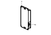
- FIG. 1 is a diagram showing an example of an interface adaptor 4 (part 1).
- FIG. 2 is a diagram showing an example of an interface adapter 4 (part 2).
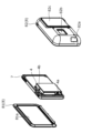
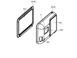
- 1 is a diagram (part 1) showing an example of a state before an interface adapter 4 and a portable information terminal 7 are accommodated in a frame 8.
- FIG. 13 is a diagram (part 2) showing an example of the state before the interface adapter 4 and the portable information terminal 7 are accommodated in the frame 8.
- FIG. 1 is a diagram (part 1) showing an example of a state in which an interface adaptor 4 and a portable information terminal 7 are attached to a rear case 82.
- FIG. 13 is a diagram (part 2) showing an example of a state in which the interface adaptor 4 and the portable information terminal 7 are attached to the rear case 82.
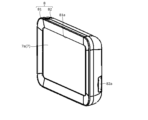
- FIG. FIG. 13 is a diagram (part 1) showing an example of a state in which a front cover 81 is attached to a rear case 82.
- FIG. 2 is a diagram (part 2) showing an example of a state in which the front cover 81 is attached to the rear case 82.
- 2 is a diagram showing an example of the internal configuration of a scope 1 and an interface adapter 4.
- FIG. 2 is a diagram illustrating an example of a hardware configuration of a portable information terminal 7. 4 is a flowchart for explaining a detailed example of photometry processing and exposure control performed by a system control unit 44.
- FIG. 11 is a schematic diagram illustrating the relationship between the magnitude of the exposure change amount ⁇ EV [Log] and the exposure time SS and the amplification factor DG.
- FIG. FIG. 11 is a schematic diagram for explaining gamma correction processing.
- 7 is a schematic diagram showing an example of an image displayed on the display unit 7a when the scope 1 is a bronchial endoscope.
- FIG. 5 is a diagram showing a display example of image data that has been gamma-corrected so as to have the output gradation characteristics shown by the solid line in graph 53.
- FIG. FIG. 13 is a diagram illustrating an example of a gain correction table.
- Fig. 1 is a diagram showing an example of an endoscope system 100 according to an embodiment of the present invention.
- the endoscope system 100 includes a scope 1, an interface adapter 4 connected to the scope 1, and a frame 8 that houses a portable information terminal 7 connected to the interface adapter 4. Note that the interface adapter 4 is located behind the portable information terminal 7 and covered by the frame 8 in Fig. 1, and is therefore not visible.
- the endoscope system 100 may further include the portable information terminal 7.
- the scope 1 is an endoscope that includes an insertion section 10, which is a tubular member extending in one direction and is inserted into a subject, and an operation section 11 that is provided at the base end of the insertion section 10 and is used to perform various operations on the scope 1.
- the operation section 11 includes, for example, an angle knob that bends the insertion section 10 by a rotation operation.
- the operation section 11 may also include operation members for performing operations such as switching the observation mode of the scope 1, image capture and recording operations, forceps operations, air and water supply operations, and suction operations.
- the scope 1 is connected to the interface adapter 4 via the communication cable 13.
- the scope 1 is also detachable from the interface adapter 4 via the communication cable 13, and can be used once (i.e., disposable).
- the communication cable 13 may be detachable from the interface adapter 4, or the scope 1 may be detachable from the communication cable 13.
- various channels such as a forceps hole for inserting forceps to collect biological tissue such as cells or polyps, channels for supplying air and water, and a suction channel may be provided inside the operation unit 11 and the insertion unit 10.
- the insertion section 10 is composed of a flexible soft section 10A, a bending section 10B provided at the tip of the flexible section 10A, and a rigid tip section 10C provided at the tip of the bending section 10B.
- the bending section 10B is configured to be freely bent by operating the operating section 11 (e.g., an angle knob). This bending section 10B can be bent in any direction and at any angle depending on the part of the subject on which the scope 1 is used, etc., and the tip section 10C can be pointed in the desired direction.
- the interface adapter 4 connects the scope 1 and the portable information terminal 7. Specifically, the interface adapter 4 is communicatively connected to the scope 1 via, for example, a communication cable 13. The interface adapter 4 is also communicatively connected to the portable information terminal 7 via a wired or wireless connection.
- the interface adapter 4 also receives from the scope 1 an imaging signal obtained by imaging the inside of the subject using the imaging sensor of the scope 1, and converts the received imaging signal into image data that can be displayed by the portable information terminal 7. The interface adapter 4 then transmits the converted image data to the portable information terminal.
- the portable information terminal 7 is a general-purpose portable information terminal such as a tablet terminal or a smartphone.
- the portable information terminal 7 has a display unit 7a that can display images based on image data.
- the portable information terminal 7 receives captured images obtained by imaging the inside of the subject with the scope 1 from the interface adapter 4, and displays the received captured images on the display unit 7a.
- the display unit 7a has a display surface on which display pixels are arranged two-dimensionally, and pixel data constituting image data is drawn on each display pixel of this display surface, thereby displaying an image based on this image data.
- the portable information terminal 7 also serves as a user interface that controls the interface adapter 4.
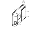
- Figures 2 and 3 are diagrams showing an example of the interface adapter 4.
- Figures 2 and 3 show the interface adapter 4 viewed from different directions.
- the interface adapter 4 has a substantially rectangular parallelepiped shape and has a video input terminal 4a and a video output terminal 4b.
- Each of the video input terminal 4a and the video output terminal 4b can be a terminal of various communication standards capable of transmitting video signals, such as USB (Universal Serial Bus), HDMI (High-Definition Multimedia Interface), and DVI (Digital Visual Interface).
- USB Universal Serial Bus
- HDMI High-Definition Multimedia Interface
- DVI Digital Visual Interface
- Video input terminal 4a is a terminal for connecting to scope 1 so as to be able to communicate with it.
- video input terminal 4a is an HDMI terminal
- scope 1 is also provided with an HDMI terminal.
- communication cable 13 is an HDMI cable, and video input terminal 4a and the HDMI terminal of scope 1 are connected by communication cable 13.
- connection between the interface adapter 4 and the scope 1 is not limited to an HDMI connection, and may be a wired connection other than HDMI, such as USB or DVI, or a wireless connection such as Bluetooth or short-range wireless communication. Bluetooth is a registered trademark.
- the connection between the interface adapter 4 and the scope 1 may also be made via a conversion adapter that converts communication standards.
- the video output terminal 4b is a terminal for connecting to the portable information terminal 7 so as to be able to communicate with it.
- the video output terminal 4b is a USB terminal
- the portable information terminal 7 is also provided with a USB terminal.
- the video output terminal 4b and the USB terminal of the portable information terminal 7 are connected by a USB cable.
- connection between the interface adapter 4 and the portable information terminal 7 is not limited to a USB connection, and may be a wired connection other than USB, such as HDMI or DVI, or a wireless connection such as Bluetooth or short-range wireless communication.
- the connection between the interface adapter 4 and the portable information terminal 7 may also be made via a conversion adapter that converts communication standards.
- the interface adapter 4 Inside the interface adapter 4, there is provided a circuit that controls the scope 1 and converts the image signal from the scope 1 into image data that can be displayed by the portable information terminal 7.
- the internal configuration of the interface adapter 4 will be described later (see, for example, FIG. 10).
- FIGState of the interface adapter 4 and the portable information terminal 7 before being accommodated in the frame 8 are diagrams showing an example of the interface adapter 4 and the portable information terminal 7 before they are housed in the frame 8.
- Figures 4 and 5 show the interface adapter 4, the portable information terminal 7, and the frame 8 viewed from different directions.
- the frame 8 includes a front cover 81 and a rear case 82.
- the front cover 81 is a member that protects the front surface of the portable information terminal 7.
- the front cover 81 has an opening 81a for exposing the display unit 7a (touch panel) of the portable information terminal 7 from the front cover 81 so that display on the display unit 7a and touch operation on the display unit 7a are possible.
- the rear case 82 is a member that protects the rear surface of the portable information terminal 7.
- the rear case 82 is also provided with a cable insertion hole (not shown) so that a communication cable 13 can be connected from outside the frame 8 to the video input terminal 4a of the interface adapter 4 housed in the frame 8, and the rear case 82 is provided with a cable insertion hole cover 82a that covers this cable insertion hole.
- the rear case 82 is also provided with a notation viewing hole 82b so that notations such as standard compliance on the housing of the interface adapter 4 can be viewed from outside the frame 8.
- the interface adapter 4 is housed in the frame 8 together with the portable information terminal 7, thereby fixing the interface adapter 4 to the frame 8.
- the interface adapter 4 is attached to the back surface of the portable information terminal 7 fixed by the frame 8, and is thereby fixed to the frame 8 via the portable information terminal 7.
- the interface adapter 4 is attached to the portable information terminal 7, for example, by screwing into screw holes provided on the back of the portable information terminal 7.
- the interface adapter 4 may also be attached to the portable information terminal 7 via a metal plate or the like formed to match the shape of the back of the interface adapter 4.
- the interface adapter 4 is not limited to being fixed to the frame 8 via the portable information terminal 7, and may be attached directly to the frame 8.
- the interface adapter 4 may be attached to the rear case 82 of the frame 8.
- a stand 82c may also be provided on the outside of the rear case 82.
- the stand 82c is provided on the rear case 82 via a hinge, for example, and by pulling out a portion of the stand 82c from the rear case 82, the frame 8 can be placed upright on a horizontal surface such as a table top.
- the rear case 82 may be provided with screw holes that can be used to attach the frame 8 to a wall mount, arm, stand, or the like. These screw holes may be compliant with, for example, the VESA (Video Electronics Standards Association) standard.
- VESA Video Electronics Standards Association
- the video output terminal 4b of the interface adapter 4 and the portable information terminal 7 are connected via a communication cable (e.g., a USB cable).
- a communication cable e.g., a USB cable
- Figures 6 and 7 are diagrams showing an example of the interface adapter 4 and portable information terminal 7 attached to the rear case 82.
- Figures 6 and 7 show the interface adapter 4, portable information terminal 7, and frame 8 viewed from different directions.
- the portable information terminal 7 and the interface adapter 4 are attached to the inside of the rear case 82 as shown in Figures 6 and 7. This exposes the markings on the housing of the interface adapter 4, such as standard compliance, from the marking viewing hole 82b.
- the video input terminal 4a of the interface adapter 4 is exposed from the cable insertion hole of the rear case 82.
- FIG. 8 and 9 are diagrams showing an example of a state in which the front cover 81 is attached to the rear case 82.
- Fig. 8 and Fig. 9 show the frame 8 and the like as viewed from different directions.
- the front cover 81 is attached to the rear case 82 as shown in Figures 8 and 9. This causes the portable information terminal 7 and interface adapter 4 to be housed in the frame 8.
- the frame 8 has a waterproof structure to prevent the intrusion of water, dust, and the like from the outside.
- a packing is provided between the front cover 81 and the rear case 82 to fill the seam between the front cover 81 and the rear case 82.
- the frame of the opening 81a of the front cover 81 is sealed so as to be in close contact with the display unit 7a of the portable information terminal 7, and the opening 81a is blocked by the display unit 7a.
- the frame of the notation viewing hole 82b of the rear case 82 is sealed so as to fit closely with the housing of the interface adapter 4, and the notation viewing hole 82b is blocked by the housing of the interface adapter 4.
- the frame of the cable insertion hole of the rear case 82 is sealed so as to fit closely with the housing of the interface adapter 4, and when the cable insertion hole cover 82a is removed from the rear case 82, the cable insertion hole of the rear case 82 is blocked by the housing of the interface adapter 4. Furthermore, when the cable insertion hole cover 82a is removed from the rear case 82, the periphery of the cable insertion hole of the rear case 82 is sealed so that the cable insertion hole of the rear case 82 is blocked by the communication cable 13 inserted from the cable insertion hole of the rear case 82.
- the frame 8 has a waterproof structure that prevents water, dust, etc. from entering the inside of the frame 8 by utilizing the interface adapter 4 and portable information terminal 7 that it accommodates.
- the portable information terminal 7, interface adapter 4, and frame 8 are used in an outdoor environment, it is possible to prevent water, dust, etc. from entering the inside of the frame 8 and protect the interface adapter 4 and portable information terminal 7.
- the endoscope system 100 is configured such that the interface adapter 4, which converts the image signal obtained by the imaging sensor 23 of the scope 1 into image data that can be displayed by the portable information terminal 7, is fixed to the frame 8 that houses the portable information terminal 7.
- the interface adapter 4 converts the image signal obtained by the imaging sensor 23 of the scope 1 into image data, so the portable information terminal 7 can be a general-purpose portable information terminal such as a tablet terminal. This makes it easy to procure, replace, update, etc. the portable information terminal 7.
- the interface adapter 4 is fixed to the frame 8 that houses the portable information terminal 7, the portable information terminal 7 and the interface adapter 4 are integrated by the frame 8. This makes it easier to handle the scope 1 when operating it while observing, on the portable information terminal 7, an image based on an imaging signal obtained by the imaging sensor 23 of the scope 1.
- a user of the endoscope system 100 can operate the scope 1 while observing an image, without having to worry about the position of the interface adapter 4 between the scope 1 and the portable information terminal 7.
- a user of the endoscope system 100 e.g., a doctor, etc.
- can operate the scope 1 while observing an image without having to worry about the position of the interface adapter 4 between the scope 1 and the portable information terminal 7.
- the user operates the scope 1 while observing an image it is possible to prevent accidents such as the interface adapter 4 between the scope 1 and the portable information terminal 7 falling and pulling the scope 1.
- an interface adapter 4 between the scope 1 and the portable information terminal 7 it is not necessary to provide the scope 1 with an image processing circuit (e.g., a signal processing unit 42) that converts the image signal obtained by the imaging sensor 23 of the scope 1 into image data, which reduces the manufacturing cost of the scope 1 and makes it easier to operate the scope 1 for single use.
- an image processing circuit e.g., a signal processing unit 42
- Fig. 10 is a diagram showing an example of the internal configuration of the scope 1 and the interface adapter 4.
- the tip portion 10C of the scope 1 is provided with an imaging optical system including an objective lens 21 and a lens group 22, an imaging sensor 23 that images a subject through the imaging optical system, a memory 25 such as a RAM (Random Access Memory), a communication interface (I/F) 26, an imaging drive unit 27, a light source device 5, and an illumination lens 50.
- an imaging optical system including an objective lens 21 and a lens group 22, an imaging sensor 23 that images a subject through the imaging optical system, a memory 25 such as a RAM (Random Access Memory), a communication interface (I/F) 26, an imaging drive unit 27, a light source device 5, and an illumination lens 50.
- the imaging sensor 23 a CCD (Charge Coupled Device) image sensor or a CMOS (Complementary Metal Oxide Semiconductor) image sensor or the like is used.
- the imaging sensor 23 may be one that performs imaging using a rolling shutter method or one that performs imaging using a global shutter method.
- the imaging sensor 23 has a light-receiving surface on which multiple pixels are arranged two-dimensionally, and converts the optical image formed on this light-receiving surface by the imaging optical system into an electrical signal (imaging signal) at each pixel.
- the imaging sensor 23 then converts the converted imaging signal from an analog signal to a digital signal with a predetermined number of bits, and outputs the digitally converted imaging signal to the memory 25.
- the imaging sensor 23 used is one equipped with color filters of primary colors or complementary colors, for example.
- the collection of imaging signals output from each pixel on the light-receiving surface of the imaging sensor 23 is called an imaging image signal.
- the memory 25 temporarily records the digital imaging signal output from the imaging sensor 23.
- the communication interface (I/F) 26 is connected to the first communication interface (I/F) 41 of the interface adapter 4.
- the communication interface 26 transmits the imaging signal recorded in the memory 25 to the interface adapter 4 through a signal line in the communication cable 13.
- the imaging driver 27 is connected to the system controller 44 of the interface adapter 4 via the communication interface 26.
- the imaging driver 27 drives the imaging sensor 23 and memory 25 based on commands from the system controller 44 received via the communication interface 26.
- the light source device 5 can emit, as illumination light, normal light, such as white light, having an emission spectrum suitable for recognition by a human being, such as a doctor. Furthermore, the light source device 5 can emit, as illumination light, special light, which has an emission spectrum different from that of normal light and has an emission spectrum suitable for image analysis by a computer, such as IEE (Image-Enhanced Endoscopy). As the light source of the light source device 5, for example, a semiconductor light source is used.
- the light source device 5 is connected to the system control unit 44 of the interface adapter 4 via the communication interface 26.
- the light source device 5 emits illumination light based on commands from the system control unit 44 received via the communication interface 26.
- the illumination lens 50 irradiates the illumination light emitted from the light source device 5 toward the object to be imaged by the imaging sensor 23 and the imaging optical system (e.g., inside the subject).
- An aperture may be included between the illumination lens 50 and the light source device 5 or in the imaging optical system, but from the viewpoint of reducing the manufacturing costs of the scope 1, it is preferable that an aperture is not included.
- the exposure control of the scope 1 can be simplified, and the manufacturing costs of the interface adapter 4 can also be reduced.
- the interface adapter 4 includes a first communication interface 41 that is connected to the communication interface 26 of the scope 1 via a communication cable 13, a signal processing unit 42, a second communication interface (I/F) 43, and a system control unit 44.
- the first communication interface 41 is for communicating with the scope 1, and has, for example, the video input terminal 4a shown in Figures 2 and 3, and receives the imaging signal transmitted from the communication interface 26 of the scope 1 via the communication cable 13 and transmits it to the signal processing unit 42.
- the signal processing unit 42 has a built-in memory such as a RAM that temporarily records the digital imaging signal received from the first communication interface 41, and processes the imaging image signal, which is a collection of imaging signals recorded in the memory (image processing such as amplification processing that amplifies each imaging signal, demosaic processing, white balance processing, or gamma correction processing), to generate image data in a format that can be displayed on the portable information terminal 7, which is a general-purpose terminal.
- the white balance gain may be written to a memory mounted on the scope 1 during manufacture so that the white balance processing can be set for each imaging sensor, and the white balance gain may be read out from this memory and used during white balance processing. From the standpoint of reducing manufacturing costs, a fixed white balance gain may be used in white balance processing.
- the second communication interface 43 is for communicating with the portable information terminal 7, and has, for example, the video output terminal 4b shown in FIG. 3, etc., and transmits image data generated by the signal processing unit 42 to the portable information terminal 7.
- the system control unit 44 controls each part of the interface adapter 4, sends commands to the scope 1, and generally controls the entire endoscope system 100.
- the system control unit 44 is an example of a control unit of the image sensor 23 that controls imaging by the image sensor 23 via the imaging drive unit 27.
- the system control unit 44 is also an example of a control unit of the light source device 5 that controls the irradiation of illumination light by the light source device 5.
- the system control unit 44 causes the image sensor 23 to perform imaging while controlling the amount of illumination light irradiated from the light source device 5 to be constant.
- the system control unit 44 also performs photometry processing to derive a photometric value (hereinafter referred to as brightness Y) indicating the brightness of the image data based on the captured image signal obtained by the imaging sensor 23, and exposure control to control the imaging sensitivity of the imaging sensor 23 (specifically, the amplification factor of the imaging signal in the above-mentioned amplification processing) and the exposure time of the imaging sensor 23 based on the brightness Y obtained by the photometry processing.
- a photometric value hereinafter referred to as brightness Y
- exposure control to control the imaging sensitivity of the imaging sensor 23 (specifically, the amplification factor of the imaging signal in the above-mentioned amplification processing) and the exposure time of the imaging sensor 23 based on the brightness Y obtained by the photometry processing.
- the system control unit 44 derives the brightness YA of the captured image signal based on the captured image signal before the amplification processing by the signal processing unit 42, amplifies this brightness YA by the amplification factor used in the amplification processing to derive the brightness Y, and controls the imaging sensitivity of the imaging sensor 23 and the exposure time of the imaging sensor 23 so that the brightness Y approaches a brightness suitable for recognition by a person such as a doctor (hereinafter referred to as target brightness Yt).
- target brightness Yt a brightness suitable for recognition by a person such as a doctor
- the signal processing unit 42 and the system control unit 44 each include various processors that execute programs to perform processing, a RAM, and a ROM (Read Only Memory).
- the various processors include a CPU (Central Processing Unit), which is a general-purpose processor that executes programs to perform various processing, a programmable logic device (PLD), which is a processor whose circuit configuration can be changed after manufacture such as an FPGA (Field Programmable Gate Array), or a dedicated electric circuit, which is a processor with a circuit configuration designed specifically to perform specific processing such as an ASIC (Application Specific Integrated Circuit). More specifically, the structure of these various processors is an electric circuit that combines circuit elements such as semiconductor elements.
- a CPU Central Processing Unit
- PLD programmable logic device
- FPGA Field Programmable Gate Array
- ASIC Application Specific Integrated Circuit
- the signal processing unit 42 and the system control unit 44 may be configured with one of various processors, or may be configured with a combination of two or more processors of the same or different types (for example, a combination of multiple FPGAs or a combination of a CPU and an FPGA). From the viewpoint of reducing the cost and size of the interface adapter 4, it is preferable that the signal processing unit 42 and the system control unit 44 are configured with only FPGAs.
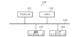
- Fig. 11 is a diagram showing an example of a hardware configuration of a portable information terminal 7.
- the portable information terminal 7 can be realized, for example, by a general-purpose information terminal 110 shown in Fig. 11.
- the information terminal 110 includes a processor 111, a memory 112, a communication interface 113, and a user interface 114.
- the processor 111, the memory 112, the communication interface 113, and the user interface 114 are connected by, for example, a bus 119.
- the processor 111 is a circuit that performs signal processing, and is, for example, a CPU (Central Processing Unit) that controls the entire information terminal 110.
- the processor 111 may be realized by other digital circuits such as an FPGA (Field Programmable Gate Array) or a DSP (Digital Signal Processor).
- the processor 111 may also be realized by combining multiple digital circuits.
- Memory 112 includes, for example, a main memory and an auxiliary memory.
- the main memory is, for example, a RAM.
- the main memory is used as a work area for processor 111.
- the auxiliary memory is a non-volatile memory such as a magnetic disk, optical disk, or flash memory.
- Various programs that operate the information terminal 110 are stored in the auxiliary memory.
- the programs stored in the auxiliary memory are loaded into the main memory and executed by the processor 111.
- the auxiliary memory may also include a portable memory that is removable from the information terminal 110.
- Portable memories include USB flash drives and memory cards such as SD (Secure Digital) memory cards.
- the communication interface 113 is a communication interface that communicates with the outside of the information terminal 110 (e.g., the interface adapter 4).
- the communication interface 113 is a wired communication interface that has a terminal that can be connected to the video output terminal 4b of the interface adapter 4 via a communication cable.
- the communication interface 113 may be a wireless communication interface that can perform wireless communication with the interface adapter 4.
- the communication interface 113 is controlled by the processor 111.
- the user interface 114 includes, for example, an input device that accepts operational input from the user, and an output device that outputs information to the user.
- the input device and the output device are realized by the display unit 7a configured as a touch panel.
- the user interface 114 may also include keys, a remote control, etc. as input devices.
- the user interface 114 may also include a speaker, a vibrator, etc. as output devices.
- the user interface 114 is controlled by the processor 111.
- the touch panel included in the user interface 114 displays image data received from the interface adapter 4 via the communication interface 113. This makes it possible to display an image based on the imaging signal obtained by the imaging sensor 23 of the scope 1 to a user such as a doctor.
- the touch panel included in the user interface 114 receives, through user operation, instructions for imaging by the imaging sensor 23 of the scope 1 and instructions for irradiating illumination light by the light source device 5 of the scope 1.
- a control signal indicating the user operation received by the user interface 114 is transmitted to the system control unit 44 of the interface adapter 4 via the communication interface 113. Based on the received control signal, the system control unit 44 controls imaging by the imaging sensor 23 of the scope 1 and controls irradiating illumination light by the light source device 5 of the scope 1.
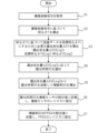
- (Detailed example of photometry processing and exposure control) 12 is a flowchart for explaining a detailed example of the photometry process and exposure control performed by the system control unit 44. In the following, a detailed example of the photometry process and exposure control will be explained assuming that the system control unit 44 is composed of only an FPGA.
- a value obtained by converting each of a plurality of exposure times that can be set in the image sensor 23 into information in logarithmic space by a logarithmic conversion lookup table (hereinafter referred to as the first LUT) is described as an exposure time SS, and a value obtained by converting each of a plurality of settable amplification factors (digital gains) used in the amplification process performed by the signal processing unit 42 into information in logarithmic space by the first LUT is described as an amplification factor DG.
- the system control unit 44 When the system control unit 44 acquires the captured image signal before it is amplified by the signal processing unit 42 (step S1), it performs a photometric calculation on the captured image signal using a predetermined photometric method to derive the brightness YA, and multiplies the brightness YA by the amplification rate currently set for the above-mentioned amplification process to derive the brightness Y (step S2).
- the photometric method is not particularly limited, but in the case of an endoscope, for example, a method of obtaining a photometric value by changing the weighting between the center and periphery of the captured image signal can be preferably used. In this case, the following formula (1) is calculated to derive the image features required to derive the photometric value.
- Image feature amount ⁇ central luminance value+(100 ⁇ ) ⁇ peripheral luminance value ⁇ 100 (1)
- ⁇ is a coefficient for changing the weighting of the central and peripheral areas, and may be a fixed value determined by the system, or may be a variable value selected from multiple values depending on the imaging mode, user preference, etc.
- the division formula shown in formula (1) can be replaced with an arithmetic formula that does not include division, as in formula (2) below, by utilizing a bit shift operation.
- ⁇ is a coefficient corresponding to ⁇ .
- Image feature value ⁇ center luminance value+(256 ⁇ ) ⁇ periphery luminance value ⁇ >>8 (2) If ⁇ in equation (1) is, for example, 20, then ⁇ in equation (2) becomes 51. If ⁇ in equation (1) is, for example, 40, then ⁇ in equation (2) becomes 102. If ⁇ in equation (1) is, for example, 60, then ⁇ in equation (2) becomes 154. If ⁇ in equation (1) is, for example, 80, then ⁇ in equation (2) becomes 205.
- the system control unit 44 may derive the image feature quantity using either equation (1) or equation (2), but if the system control unit 44 is configured only with an FPGA, it is preferable to derive the image feature quantity in step S2 using the calculation shown in equation (2) and use the image feature quantity to derive the brightness Y (photometric value).
- the calculation shown in equation (2) does not include division, and is performed using only addition and multiplication. This makes it possible to reduce the circuit size of the FPGA and improve the calculation speed by the FPGA.
- the system control unit 44 derives the exposure change amount ⁇ EV required to bring the image data to the target brightness Yt based on the brightness Y (step S3).
- the exposure change amount ⁇ EV can be derived, for example, by calculating the following formula (3).
- Exposure change ⁇ EV target brightness Yt ⁇ brightness Y (3)
- equation (3) By converting the target brightness Yt and brightness Y into logarithmic space information, equation (3) can be replaced with an arithmetic expression that does not include division, as in equation (4) below. [Log] indicates that the information is in logarithmic space.
- Exposure change amount ⁇ EV [Log] target brightness Yt [Log] - brightness Y [Log] (4)
- Target brightness Yt [Log] is the value obtained by converting target brightness Yt into information in logarithmic space using the first LUT.
- Brightness Y [Log] is the value obtained by converting brightness Y into information in logarithmic space using the first LUT.
- the calculation shown in formula (4) does not include division, but is performed only by subtraction. In other words, the calculation shown in formula (4) is performed only by subtraction out of division and subtraction. Therefore, when the system control unit 44 is configured only by an FPGA, it is possible to reduce the circuit size of the FPGA and improve the calculation speed by the FPGA.
- step S3 the system control unit 44 converts the brightness Y to brightness Y[Log] using the first LUT, converts the target brightness Yt to target brightness Yt[Log], and subtracts the brightness Y[Log] from the target brightness Yt[Log] to derive the exposure change amount ⁇ EV[Log].
- the system control unit 44 selects one of the multiple exposure times SS depending on the magnitude of the exposure change amount ⁇ EV[Log] (step S4). For example, the system control unit 44 divides the exposure change amount ⁇ EV[Log] that is equal to or greater than zero into multiple ranges depending on its magnitude.
- FIG. 13 is a schematic diagram illustrating the relationship between the magnitude of the exposure change amount ⁇ EV [Log] and the exposure time SS and amplification factor DG.
- FIG. 13 shows an example in which six exposure times SS can be set. Note that, as an example, it is preferable to set the upper limit of the exposure time SS to (1/38) seconds and the lower limit to (1/800) seconds so that the observed image composed of image data acquired continuously appears natural.
- ranges RG1, RG2, RG3, RG4, RG5, RG6, and RG7 are set in order of the smallest exposure change amount ⁇ EV[Log].
- step S4 if the exposure change amount ⁇ EV[Log] belongs to ranges RG1 and RG2, the system control unit 44 selects the smallest value (lower limit value) of the six exposure times SS. If the exposure change amount ⁇ EV[Log] belongs to range RG3, the system control unit 44 selects the second smallest value of the six exposure times SS. If the exposure change amount ⁇ EV[Log] belongs to range RG4, the system control unit 44 selects the third smallest value of the six exposure times SS.
- the system control unit 44 selects the fourth smallest value of the six exposure times SS. If the exposure change amount ⁇ EV[Log] falls within range RG6, the system control unit 44 selects the fifth smallest value among the six exposure times SS. If the exposure change amount ⁇ EV[Log] falls within range RG7, the system control unit 44 selects the maximum value among the six exposure times SS (the upper limit value of the exposure time SS).
- the range RG1 shown in FIG. 13 is the range in which exposure cannot be reduced any further, and is the range in which the generated image data is brighter than or equal to the target brightness Yt.
- the exposure change amount ⁇ EV[Log] falls within range RG1
- the lower limit value is selected for the exposure time SS, and a reference value (e.g., 1x) is selected for the amplification factor DG.
- step S5 the system control unit 44 derives the amplification factor DG by the calculation of the following equation (5) (step S5).
- Amplification rate DG exposure change amount ⁇ EV [Log] ⁇ exposure time SS (5)
- Amplification factor DG [real number] Exposure change amount ⁇ EV [real number] ⁇ Exposure time SS [real number] (6)
- the amount of illumination light is constant and the exposure value is determined by multiplying the amplification factor and exposure time, so the above formula (6) holds.
- formula (5) holds. Therefore, the amplification factor DG can be found by calculating formula (5). In this way, in step S5 as well, of the division and subtraction, only subtraction is performed. This makes it possible to reduce the circuit scale of the system control unit 44 and improve the speed at which the amplification factor DG is derived.
- the system control unit 44 determines a larger value for the amplification factor DG as the exposure change amount ⁇ EV [Log] is larger. Furthermore, in ranges RG2 to RG6, the amplification factor DG is changed within a range from a reference value to a preset value that is smaller than the upper limit value of the amplification factor DG. Furthermore, in ranges RG2 to RG6, the closer to range RG1 the range is, the larger the fluctuation range of the amplification factor DG (the difference between the reference value and the above-mentioned preset value). Meanwhile, in range RG7, the amplification factor DG is changed between the reference value and the upper limit value.
- the system control unit 44 After deriving the amplification factor DG in step S5, the system control unit 44 converts the exposure time SS selected in step S4 into a setting value for the image sensor 23 using a lookup table, and sets the setting value in the register of the image sensor 23 (step S6). As a result, in the next imaging frame, the exposure time of the image sensor 23 becomes a value equivalent to the exposure time SS selected in step S4.
- the system control unit 44 also converts the amplification factor DG derived in step S5 into a setting value for the signal processing unit 42 using a lookup table, and sets the setting value in the register of the signal processing unit 42 (step S7). As a result, in the next imaging frame, the amplification factor of the imaging signal during the amplification process becomes a value equivalent to the amplification factor DG derived in step S5.
- the exposure time of the image sensor 23 is changed discretely based on the brightness Y of the image data, and the amplification factor during the amplification process is changed continuously based on the brightness Y of the image data.
- the cost of the image sensor 23 and its control costs can be reduced.
- the brightness of the image data can be finely adjusted, and the quality of the image displayed on the portable information terminal 7 can be improved.
- the maximum value of the amplification factor DG decreases as the exposure change amount ⁇ EV[Log] moves from range RG2 to range RG6.
- the exposure change amount ⁇ EV[Log] is in range RG6
- the image data is dark and increasing the amplification factor may cause noticeable noise. Therefore, in such a situation, the signal-to-noise ratio can be improved by reducing the change range of the amplification factor.
- the exposure change amount ⁇ EV[Log] is in range RG7
- the exposure time SS has reached its upper limit, and the only way to increase the exposure is to increase the amplification factor DG. Therefore, by changing the amplification factor DG between the reference value and the upper limit, the image data can be brought closer to the target brightness even in a very dark imaging environment.
- the amplification factor DG changes depending on the magnitude of the exposure change amount ⁇ EV[Log] in each of the ranges RG2 to RG6, but this is not limited to the above.
- the amplification factor DG may remain at a reference value (equivalent to 1x) in each of the ranges RG2 to RG6. In this case, the signal-to-noise ratio can be improved in a wide range from range RG1 to range RG6.
- the signal processing unit 42 performs the above-mentioned gamma correction processing to generate image data so that when a pixel value equal to or less than the first threshold value TH1 is input to the display unit 7a, the output value of the display unit 7a is greater than the pixel value, and when a pixel value exceeding the first threshold value TH1 is input to the display unit 7a, the output value of the display unit 7a matches the pixel value.
- FIG. 14 is a schematic diagram for explaining gamma correction processing.
- the dashed straight line in graph 51 shows the ideal characteristic where the input and output are in a directly proportional relationship.
- the gamma characteristic of graph 51 is taken into consideration and gamma correction is performed on the image data before correction using correction data C1 shown in graph 52 so that when the pixel value of the corrected image data is input to the display unit 7a, the pixel value matches the output value (display luminance value) of that pixel value.
- gamma correction is performed on the image data before correction using the correction data C2 shown in graph 52.
- Graph 53 shows the relationship between the pixel value (input value) of the image data obtained by gamma correction according to the correction data C2 and the output value of the display unit 7a when that pixel value is input to the display unit 7a.
- the output gradation characteristics of the image data after gamma correction are approximately consistent with the straight line of the ideal characteristics in the range where the pixel values exceed the first threshold value TH1, and are shifted higher than the straight line of the ideal characteristics in the range where the pixel values are equal to or less than the first threshold value TH1.
- the output value of the display unit 7a is greater than that pixel value
- the output value of the display unit 7a is equal to that pixel value.
- the difference between the output value of the display unit 7a when pixel values in the second range R2 are input to the display unit 7a and that pixel value is greater than the difference between the output value of the display unit 7a when pixel values in the first range R1 are input to the display unit 7a and that pixel value.
- the slightly darker area is displayed relatively brighter.
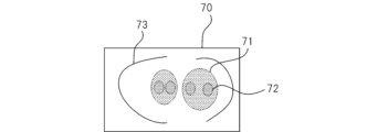
- FIG. 15 is a schematic diagram showing an example of an image displayed on the display unit 7a when the scope 1 is a bronchial endoscope.
- FIG. 15 shows an example in which the output gradation characteristics of image data after gamma correction are ideal characteristics.
- Display image 70 shows a thick tube 73, a thin tube 71, and a branch tube 72 inside thin tube 71.
- Thin tube 71 is brighter than branch tube 72, but the difference in brightness between the two is extremely slight.
- FIG. 16 is a diagram showing an example of the display of image data that has been gamma-corrected to achieve the output gradation characteristics of the solid line shown in graph 53. Between the thin tube 71 and the branch tube 72, the relatively bright thin tube 71 is displayed brighter. As a result, the state of the branch tube 72 visible within the thin tube 71 is easier to see compared to FIG. 15.
- the signal processing unit 42 does not have to use the correction data C2 of graph 52 to generate image data having the output gradation characteristics shown by the solid line of graph 53.
- the output gradation characteristics shown in graph 53 may be obtained by performing gamma correction using the correction data C1, and then applying a gain greater than 1 to small pixel values according to the gain correction table shown in FIG. 17. More preferably, the output gradation characteristics shown in graph 53 may be obtained by performing gamma correction using the correction data C1, converting the pixel values to luminance values, and then applying a gain greater than 1 to luminance values smaller than a predetermined value according to the gain correction table shown in FIG. 17.
- the imaging sensitivity of the imaging sensor 23 is changed by changing the amplification factor used in the amplification process performed by the signal processing unit 42.
- the imaging sensitivity may be changed by changing the amplification factor of an amplifier that amplifies an analog signal contained in the imaging sensor 23.
- first communication interface 41 for communicating with a scope (scope 1) including an imaging sensor (imaging sensor 23) and a light source device (light source device 5) for generating illumination light for imaging by the imaging sensor; a second communication interface (second communication interface 43) for communicating with a portable information terminal;
- a processor (a system control unit 44 and a signal processing unit 42), The processor is Executing an image capture by the image sensor while controlling the amount of light of the illumination light to a constant level; converting the captured image signal obtained by the imaging sensor into image data that can be displayed by the portable information terminal, and transmitting the image data to the portable information terminal; Deriving brightness of the image data based on the captured image signal; an interface adapter that controls the imaging sensitivity of the imaging sensor and the exposure time of the imaging sensor based on the brightness;
- exposure control is performed by adjusting two parameters, imaging sensitivity and exposure time, while the amount of illumination light is constant. Since the number of adjustments required for exposure control is narrowed down to two, advanced processor capabilities are not required. As a result, a system can be realized at low cost that can display and check images captured by a scope using a general-purpose portable information terminal connected via the second communications interface. It also becomes possible to make the interface adapter smaller and lighter.
- the interface adapter controls the exposure time to an upper limit value (when the exposure change amount ⁇ EV[Log] is in the range R7), and increases the range of fluctuation of the imaging sensitivity compared to when the exposure time is controlled to less than the upper limit value (when the exposure change amount ⁇ EV[Log] is in the range RG2 to RG6).
- the fluctuation range of the imaging sensitivity is small until the exposure time reaches the upper limit, so the signal-to-noise ratio of the imaging signal can be improved.
- the fluctuation range of the imaging sensitivity can be increased, so that a dark subject can be captured brightly.
- An interface adapter according to any one of (1) to (4), the processor performs an amplification process for amplifying the digital captured image signal output from the image sensor;
- the imaging sensitivity is an amplification factor set in the amplification process.
- the brightness of the image data can be controlled by amplifying the digital signal, so exposure control can be performed with higher precision than when controlling the amplification rate when amplifying an analog signal inside the imaging sensor.
- the manufacturing costs of the scope can be reduced.
- the processor is a programmable logic device.
- An interface adapter according to (6), The processor performs only the subtraction out of division and subtraction as a calculation process required to determine the combination of the imaging sensitivity and the exposure time to bring the brightness (brightness Y) closer to a target brightness (target brightness Yt), an interface adapter.
- An interface adapter A value obtained by logarithmically converting each of a plurality of exposure times that can be set in the image sensor is defined as an exposure time logarithm value (exposure time SS),
- the processor is subtracting the logarithmic transformation value of the brightness (brightness Y[Log]) from the logarithmic transformation value of the target brightness (target brightness Yt[Log]) to derive a first subtraction value (exposure change amount ⁇ EV[Log]); selecting one from a plurality of the exposure time logarithm values according to a magnitude of the first subtraction value; subtracting the selected logarithmic value of the exposure time from the first subtraction value to derive a second subtraction value (amplification factor DG[Log]); an interface adapter that converts the selected logarithmic value of the exposure time into a setting value of the exposure time using a conversion table (lookup table), and converts the second subtraction value into a setting value of the imaging sensitivity using a conversion table (lookup table
- division processing is no longer necessary to determine brightness, making it possible to reduce the processor circuit scale and calculation time.
- the processor is As a process for converting the captured image signal into the image data, a gamma correction process based on the gamma characteristic of a display unit (display unit 7a) of the portable information terminal is performed;
- the interface adapter In the gamma correction process, the interface adapter generates image data such that when a pixel value that is equal to or less than a first threshold value (first threshold value TH1) is input to the display unit, the output value of the display unit is greater than the pixel value, and when a pixel value that exceeds the first threshold value is input to the display unit, the output value of the display unit matches the pixel value.
- first threshold value TH1 a first threshold value
- the interface adapter Among the pixel values of the image data, a range from a minimum value to a second threshold value (second threshold value TH2) smaller than the first threshold value is defined as a first range (first range R1), and a range from a third threshold value (third threshold value TH3) between the first threshold value and the second threshold value to the second threshold value is defined as a second range (second range R2);
- the processor generates the image data in the gamma correction process such that the difference between the output value of the display unit and the pixel value when pixel values in the second range are input to the display unit is greater than the difference between the output value of the display unit and the pixel value when pixel values in the first range are input to the display unit.
- An interface adapter according to any one of (1) to (11), An interface adapter is fixed to a frame (frame 8) capable of housing the portable information terminal.
- An interface adapter according to any one of (1) to (11); A frame (frame 8) capable of housing the portable information terminal; The above-mentioned scope, An endoscope system (endoscope system 100) in which the interface adaptor is fixed to the frame.
Landscapes
- Health & Medical Sciences (AREA)
- Life Sciences & Earth Sciences (AREA)
- Surgery (AREA)
- Engineering & Computer Science (AREA)
- Physics & Mathematics (AREA)
- Biomedical Technology (AREA)
- Animal Behavior & Ethology (AREA)
- Radiology & Medical Imaging (AREA)
- Optics & Photonics (AREA)
- Nuclear Medicine, Radiotherapy & Molecular Imaging (AREA)
- Biophysics (AREA)
- Heart & Thoracic Surgery (AREA)
- Medical Informatics (AREA)
- Molecular Biology (AREA)
- Pathology (AREA)
- General Health & Medical Sciences (AREA)
- Public Health (AREA)
- Veterinary Medicine (AREA)
- Signal Processing (AREA)
- General Physics & Mathematics (AREA)
- Theoretical Computer Science (AREA)
- Endoscopes (AREA)
Abstract
Description
図1は、本発明の一実施形態である内視鏡システム100の一例を示す図である。内視鏡システム100は、スコープ1と、スコープ1と接続されるインタフェースアダプタ4と、インタフェースアダプタ4と接続される携帯型情報端末7を収容するフレーム8と、を含む。なお、インタフェースアダプタ4は、図1においては携帯型情報端末7の裏側にありフレーム8で覆われているため見えない状態である。内視鏡システム100は、さらに携帯型情報端末7を含んでもよい。
図2及び図3は、インタフェースアダプタ4の一例を示す図である。図2,図3は、それぞれ異なる方向からインタフェースアダプタ4を見た図になっている。図2,図3に示すように、インタフェースアダプタ4は、略直方体形状であり、映像入力端子4a及び映像出力端子4bを有する。
図4及び図5は、インタフェースアダプタ4及び携帯型情報端末7のフレーム8への収容前の状態の一例を示す図である。図4,図5は、それぞれ異なる方向からインタフェースアダプタ4、携帯型情報端末7、及びフレーム8を見た図になっている。図4,図5に示すように、フレーム8は、フロントカバー81と、リアケース82と、を含む。
図8及び図9は、リアケース82にフロントカバー81を取り付けた状態の一例を示す図である。図8,図9は、それぞれ異なる方向からフレーム8等を見た図になっている。
図10は、スコープ1及びインタフェースアダプタ4の内部構成の一例を示す図である。図10に示すように、スコープ1の先端部10Cには、対物レンズ21及びレンズ群22を含む撮像光学系と、この撮像光学系を通して被写体を撮像する撮像センサ23と、RAM(Random Access Memory)等のメモリ25と、通信インタフェース(I/F)26と、撮像駆動部27と、光源装置5と、照明用レンズ50と、が設けられている。
図11は、携帯型情報端末7のハードウェア構成の一例を示す図である。携帯型情報端末7は、例えば図11に示す汎用の情報端末110により実現することができる。情報端末110は、プロセッサ111と、メモリ112と、通信インタフェース113と、ユーザインタフェース114と、を備える。プロセッサ111、メモリ112、通信インタフェース113、及びユーザインタフェース114は、例えばバス119によって接続される。
図12は、システム制御部44が行う測光処理及び露出制御の詳細例を説明するためのフローチャートである。以下では、システム制御部44がFPGAのみで構成される場合を想定して、測光処理及び露出制御の詳細例を説明する。また、以下では、撮像センサ23に設定可能な複数の露光時間のそれぞれを、対数変換ルックアップテーブル(以下、第1LUTと記載)によって対数空間の情報に変換した値を露光時間SSと記載し、信号処理部42により行われる増幅処理で用いる設定可能な複数の増幅率(デジタルゲイン)のそれぞれを、第1LUTによって対数空間の情報に変換した値を増幅率DGと記載する。第1LUTは、例えば、y=Log(x)×aの式にしたがって生成されている。この式において、aは所定の係数、xは変換前の数値、yは変換後の数値である。
={α×中央部輝度値+(100-α)×周辺部輝度値}÷100 ・・(1)
式(1)のαは、中央部と周辺部の重み付けを変えるための係数であり、システム側で決められる固定値でもよいし、撮像モードやユーザの好み等によって複数の値から選択される可変値であってもよい。
={β×中央部輝度値+(256-β)×周辺部輝度値}>>8 ・・(2)
式(1)のαが例えば20であれば、式(2)のβは51となる。
式(1)のαが例えば40であれば、式(2)のβは102となる。
式(1)のαが例えば60であれば、式(2)のβは154となる。
式(1)のαが例えば80であれば、式(2)のβは205となる。
=目標明るさYt[Log]-明るさY[Log] ・・(4)
増幅率DG=露出変化量ΔEV[Log]-露光時間SS ・・(5)
=露出変化量ΔEV[実数]÷露光時間SS[実数] ・・(6)
信号処理部42は、第1閾値TH1以下となる画素値を表示部7aに入力したときの表示部7aの出力値がその画素値よりも大きくなり、第1閾値TH1を超える画素値を表示部7aに入力したときの表示部7aの出力値がその画素値と一致する状態となるように、上述したガンマ補正処理を行って画像データを生成することが好ましい。
撮像センサ(撮像センサ23)及び上記撮像センサによる撮像のための照明光を生成する光源装置(光源装置5)を含むスコープ(スコープ1)と通信するための第1通信インタフェース(第1通信インタフェース41)と、
携帯型情報端末と通信するための第2通信インタフェース(第2通信インタフェース43)と、
プロセッサ(システム制御部44及び信号処理部42)と、を備え、
上記プロセッサは、
上記照明光の光量を一定に制御した状態で上記撮像センサにより撮像を実行させ、
上記撮像センサにより得られた撮像画像信号を上記携帯型情報端末が表示可能な画像データに変換し、上記画像データを上記携帯型情報端末へ送信し、
上記撮像画像信号に基づいて上記画像データの明るさを導出し、
上記明るさに基づいて、上記撮像センサによる撮像感度と上記撮像センサの露光時間を制御する、インタフェースアダプタ。
(1)に記載のインタフェースアダプタであって、
上記プロセッサは、上記露光時間を上限値に制御する場合(露出変化量ΔEV[Log]が範囲R7の場合)には、上記露光時間を上記上限値未満に制御する場合(露出変化量ΔEV[Log]が範囲RG2から範囲RG6の場合)と比べて、上記撮像感度の変動幅を大きくする、インタフェースアダプタ。
(2)に記載のインタフェースアダプタであって、
上記プロセッサは、上記露光時間を離散的に変化させ、上記撮像感度を連続的に変化させる、インタフェースアダプタ。
(2)に記載のインタフェースアダプタであって、
上記プロセッサは、上記明るさの複数の範囲(露出変化量ΔEV[Log]が範囲RG2からRG7となる明るさの各範囲)毎に上記露光時間を異なる値に設定し、上記露光時間を上記上限値未満に制御する状態では、上記明るさに応じて、上記撮像感度を基準値(増幅率DG=1倍)から上記撮像感度の上限値よりも低い値の間で変化させる、インタフェースアダプタ。
(1)から(4)のいずれかに記載のインタフェースアダプタであって、
上記プロセッサは、上記撮像センサから出力されるデジタルの上記撮像画像信号を増幅する増幅処理を行い、
上記撮像感度は、上記増幅処理で設定される増幅率である、インタフェースアダプタ。
(1)から(5)のいずれかに記載のインタフェースアダプタであって、
上記プロセッサは、プログラマブルロジックデバイスである、インタフェースアダプタ。
(6)に記載のインタフェースアダプタであって、
上記プロセッサは、上記明るさ(明るさY)を目標明るさ(目標明るさYt)に近づけるための上記撮像感度と上記露光時間の組み合わせの決定に必要な演算処理として、除算と減算のうち上記減算のみを行う、インタフェースアダプタ。
(7)に記載のインタフェースアダプタであって、
上記撮像センサに設定可能な複数の露光時間のそれぞれを対数変換した値を露光時間対数値(露光時間SS)とし、
上記プロセッサは、
上記目標明るさの対数変換値(目標明るさYt[Log])から上記明るさの対数変換値(明るさY[Log])を減算して第1減算値(露出変化量ΔEV[Log])を導出し、
上記第1減算値の大きさに応じて複数の上記露光時間対数値から1つを選択し、
上記第1減算値から、上記選択した上記露光時間対数値を減算して第2減算値(増幅率DG[Log])を導出し、
上記選択した上記露光時間対数値を、変換テーブル(ルックアップテーブル)を用いて上記露光時間の設定値に変換し、上記第2減算値を、変換テーブル(ルックアップテーブル)を用いて上記撮像感度の設定値に変換する、インタフェースアダプタ。
(6)から(8)のいずれかに記載のインタフェースアダプタであって、
上記プロセッサは、上記明るさの判定に必要な演算をビットシフト演算によって行う、インタフェースアダプタ。
(1)から(9)のいずれかに記載のアダプタであって、
上記プロセッサは、
上記撮像画像信号を上記画像データに変換する処理として、上記携帯型情報端末の表示部(表示部7a)のガンマ特性に基づくガンマ補正処理を行い、
上記ガンマ補正処理においては、第1閾値(第1閾値TH1)以下となる画素値を上記表示部に入力したときの上記表示部の出力値がその画素値よりも大きくなり、上記第1閾値を超える画素値を上記表示部に入力したときの上記表示部の出力値がその画素値と一致する状態となる上記画像データを生成する、インタフェースアダプタ。
(10)に記載のインタフェースアダプタであって、
上記画像データの画素値のうち、最小値から上記第1閾値よりも小さい第2閾値(第2閾値TH2)までの範囲を第1範囲(第1範囲R1)とし、上記第1閾値と上記第2閾値の間の第3閾値(第3閾値TH3)から上記第2閾値までの範囲を第2範囲(第2範囲R2)とし、
上記プロセッサは、上記ガンマ補正処理においては、上記第2範囲の画素値を上記表示部に入力したときの上記表示部の出力値とその画素値との差が、上記第1範囲の画素値を上記表示部に入力したときの上記表示部の出力値とその画素値との差よりも大きくなる上記画像データを生成する、インタフェースアダプタ。
(1)から(11)のいずれかに記載のインタフェースアダプタであって、
上記携帯型情報端末を収容可能なフレーム(フレーム8)に固定される、インタフェースアダプタ。
(1)から(11)のいずれかに記載のインタフェースアダプタと、
上記携帯型情報端末を収容可能なフレーム(フレーム8)と、
上記スコープと、を備え、
上記フレームに上記インタフェースアダプタが固定される、内視鏡システム(内視鏡システム100)。
4 インタフェースアダプタ
4a 映像入力端子
4b 映像出力端子
5 光源装置
7 携帯型情報端末
7a 表示部
8 フレーム
10 挿入部
10A 軟性部
10B 湾曲部
10C 先端部
11 操作部
13 通信ケーブル
22 レンズ群
23 撮像センサ
25,112 メモリ
26,113 通信インタフェース
41 第1通信インタフェース
27 撮像駆動部
42 信号処理部
43 第2通信インタフェース
44 システム制御部 50 照明用レンズ
81 フロントカバー
81a 開口部
82 リアケース
82a ケーブル差込孔蓋
82b 表記視認孔
82c スタンド
100 内視鏡システム
110 情報端末
111 プロセッサ
114 ユーザインタフェース
119 バス
RG1~RG7 範囲
51、52、53 グラフ
C1、C2 補正データ
R1 第1範囲
R2 第2範囲
70 表示画像
71 細管
72 分岐管
73 太管
Claims (13)
- 撮像センサ及び前記撮像センサによる撮像のための照明光を生成する光源装置を含むスコープと通信するための第1通信インタフェースと、
携帯型情報端末と通信するための第2通信インタフェースと、
プロセッサと、を備え、
前記プロセッサは、
前記照明光の光量を一定に制御した状態で前記撮像センサにより撮像を実行させ、
前記撮像センサにより得られた撮像画像信号を前記携帯型情報端末が表示可能な画像データに変換し、前記画像データを前記携帯型情報端末へ送信し、
前記撮像画像信号に基づいて前記画像データの明るさを導出し、
前記明るさに基づいて、前記撮像センサによる撮像感度と前記撮像センサの露光時間を制御する、インタフェースアダプタ。 - 請求項1に記載のインタフェースアダプタであって、
前記プロセッサは、前記露光時間を上限値に制御する場合には、前記露光時間を前記上限値未満に制御する場合と比べて、前記撮像感度の変動幅を大きくする、インタフェースアダプタ。 - 請求項2に記載のインタフェースアダプタであって、
前記プロセッサは、前記露光時間を離散的に変化させ、前記撮像感度を連続的に変化させる、インタフェースアダプタ。 - 請求項2に記載のインタフェースアダプタであって、
前記プロセッサは、前記明るさの複数の範囲毎に前記露光時間を異なる値に設定し、前記露光時間が前記上限値未満に設定される状態では、前記明るさに応じて、前記撮像感度を基準値から前記撮像感度の上限値よりも低い値の間で変化させる、インタフェースアダプタ。 - 請求項1から4のいずれか1項に記載のインタフェースアダプタであって、
前記プロセッサは、前記撮像センサから出力されるデジタルの前記撮像画像信号を増幅する増幅処理を行い、
前記撮像感度は、前記増幅処理で設定される増幅率である、インタフェースアダプタ。 - 請求項1から4のいずれか1項に記載のインタフェースアダプタであって、
前記プロセッサは、プログラマブルロジックデバイスである、インタフェースアダプタ。 - 請求項6に記載のインタフェースアダプタであって、
前記プロセッサは、前記明るさを目標明るさに近づけるための前記撮像感度と前記露光時間の組み合わせの決定に必要な演算処理として、除算と減算のうち前記減算のみを行う、インタフェースアダプタ。 - 請求項7に記載のインタフェースアダプタであって、
前記撮像センサに設定可能な複数の露光時間のそれぞれを対数変換した値を露光時間対数値とし、
前記プロセッサは、
前記目標明るさの対数変換値から前記明るさの対数変換値を減算して第1減算値を導出し、
前記第1減算値の大きさに応じて複数の前記露光時間対数値から1つを選択し、
前記第1減算値から、前記選択した前記露光時間対数値を減算して第2減算値を導出し、
前記選択した前記露光時間対数値を、変換テーブルを用いて前記露光時間の設定値に変換し、前記第2減算値を、変換テーブルを用いて前記撮像感度の設定値に変換する、インタフェースアダプタ。 - 請求項6に記載のインタフェースアダプタであって、
前記プロセッサは、前記明るさの判定に必要な演算をビットシフト演算によって行う、インタフェースアダプタ。 - 請求項1から4のいずれか1項に記載のアダプタであって、
前記プロセッサは、
前記撮像画像信号を前記画像データに変換する処理として、前記携帯型情報端末の表示部のガンマ特性に基づくガンマ補正処理を行い、
前記ガンマ補正処理においては、第1閾値以下となる画素値を前記表示部に入力したときの前記表示部の出力値が当該画素値よりも大きくなり、前記第1閾値を超える画素値を前記表示部に入力したときの前記表示部の出力値が当該画素値と一致する状態となる前記画像データを生成する、インタフェースアダプタ。 - 請求項10に記載のインタフェースアダプタであって、
前記画像データの画素値のうち、最小値から前記第1閾値よりも小さい第2閾値までの範囲を第1範囲とし、前記第1閾値と前記第2閾値の間の第3閾値から前記第2閾値までの範囲を第2範囲とし、
前記プロセッサは、前記ガンマ補正処理においては、前記第2範囲の画素値を前記表示部に入力したときの前記表示部の出力値と当該画素値との差が、前記第1範囲の画素値を前記表示部に入力したときの前記表示部の出力値と当該画素値との差よりも大きくなる前記画像データを生成する、インタフェースアダプタ。 - 請求項1から4のいずれか1項に記載のインタフェースアダプタであって、
前記携帯型情報端末を収容可能なフレームに固定される、インタフェースアダプタ。 - 請求項1から4のいずれか1項に記載のインタフェースアダプタと、
前記携帯型情報端末を収容可能なフレームと、
前記スコープと、を備え、
前記フレームに前記インタフェースアダプタが固定される、内視鏡システム。
Priority Applications (4)
| Application Number | Priority Date | Filing Date | Title |
|---|---|---|---|
| JP2025502137A JPWO2024176602A1 (ja) | 2023-02-22 | 2023-12-20 | |
| CN202380094171.2A CN120693097A (zh) | 2023-02-22 | 2023-12-20 | 内窥镜系统及接口适配器 |
| DE112023005845.8T DE112023005845T5 (de) | 2023-02-22 | 2023-12-20 | Endoskopsystem und schnittstellenadapter |
| US19/300,687 US20250375094A1 (en) | 2023-02-22 | 2025-08-15 | Endoscope system and interface adapter |
Applications Claiming Priority (2)
| Application Number | Priority Date | Filing Date | Title |
|---|---|---|---|
| JP2023-025924 | 2023-02-22 | ||
| JP2023025924 | 2023-02-22 |
Related Child Applications (1)
| Application Number | Title | Priority Date | Filing Date |
|---|---|---|---|
| US19/300,687 Continuation US20250375094A1 (en) | 2023-02-22 | 2025-08-15 | Endoscope system and interface adapter |
Publications (1)
| Publication Number | Publication Date |
|---|---|
| WO2024176602A1 true WO2024176602A1 (ja) | 2024-08-29 |
Family
ID=92500876
Family Applications (1)
| Application Number | Title | Priority Date | Filing Date |
|---|---|---|---|
| PCT/JP2023/045789 Ceased WO2024176602A1 (ja) | 2023-02-22 | 2023-12-20 | 内視鏡システム及びインタフェースアダプタ |
Country Status (5)
| Country | Link |
|---|---|
| US (1) | US20250375094A1 (ja) |
| JP (1) | JPWO2024176602A1 (ja) |
| CN (1) | CN120693097A (ja) |
| DE (1) | DE112023005845T5 (ja) |
| WO (1) | WO2024176602A1 (ja) |
Citations (4)
| Publication number | Priority date | Publication date | Assignee | Title |
|---|---|---|---|---|
| JP2000330037A (ja) * | 1999-05-24 | 2000-11-30 | Olympus Optical Co Ltd | 内視鏡用写真撮影装置 |
| JP2017528177A (ja) * | 2014-07-02 | 2017-09-28 | ゼノコア インコーポレイテッド | ボアスコープ並びに関係する方法及びシステム |
| CN111948798A (zh) * | 2020-08-21 | 2020-11-17 | 微创(上海)医疗机器人有限公司 | 内窥镜系统及用于检测内窥镜的末端与组织接触的方法 |
| JP2021065280A (ja) * | 2019-10-18 | 2021-04-30 | Hoya株式会社 | 内視鏡システム |
-
2023
- 2023-12-20 WO PCT/JP2023/045789 patent/WO2024176602A1/ja not_active Ceased
- 2023-12-20 CN CN202380094171.2A patent/CN120693097A/zh active Pending
- 2023-12-20 JP JP2025502137A patent/JPWO2024176602A1/ja active Pending
- 2023-12-20 DE DE112023005845.8T patent/DE112023005845T5/de active Pending
-
2025
- 2025-08-15 US US19/300,687 patent/US20250375094A1/en active Pending
Patent Citations (4)
| Publication number | Priority date | Publication date | Assignee | Title |
|---|---|---|---|---|
| JP2000330037A (ja) * | 1999-05-24 | 2000-11-30 | Olympus Optical Co Ltd | 内視鏡用写真撮影装置 |
| JP2017528177A (ja) * | 2014-07-02 | 2017-09-28 | ゼノコア インコーポレイテッド | ボアスコープ並びに関係する方法及びシステム |
| JP2021065280A (ja) * | 2019-10-18 | 2021-04-30 | Hoya株式会社 | 内視鏡システム |
| CN111948798A (zh) * | 2020-08-21 | 2020-11-17 | 微创(上海)医疗机器人有限公司 | 内窥镜系统及用于检测内窥镜的末端与组织接触的方法 |
Also Published As
| Publication number | Publication date |
|---|---|
| JPWO2024176602A1 (ja) | 2024-08-29 |
| DE112023005845T5 (de) | 2025-12-04 |
| CN120693097A (zh) | 2025-09-23 |
| US20250375094A1 (en) | 2025-12-11 |
Similar Documents
| Publication | Publication Date | Title |
|---|---|---|
| JP6109456B1 (ja) | 画像処理装置および撮像システム | |
| JP5669997B1 (ja) | 撮像装置 | |
| US20170238791A1 (en) | Endoscope system | |
| JP2009104547A (ja) | 画像処理装置、画像処理システムおよび画像処理プログラム | |
| US20100201840A1 (en) | Image pickup device, image processing method, and storage medium | |
| JP5244164B2 (ja) | 内視鏡装置 | |
| US10939801B2 (en) | Electronic endoscope system | |
| JP2009240531A (ja) | 撮影装置 | |
| JPWO2016104386A1 (ja) | 内視鏡システム | |
| JP2018138139A (ja) | 医療用撮像装置、及び医療用観察システム | |
| WO2024176602A1 (ja) | 内視鏡システム及びインタフェースアダプタ | |
| US10462440B2 (en) | Image processing apparatus | |
| US11160443B2 (en) | Electronic endoscope device for changing observation image brightness | |
| WO2020039716A1 (ja) | 医療用制御装置及び医療用観察装置 | |
| CN110168604B (zh) | 图像处理装置、图像处理方法和存储介质 | |
| JP2009105844A (ja) | 画像処理装置、画像処理システムおよび画像処理プログラム | |
| JP7587991B2 (ja) | 医療用制御装置及び医療用観察システム | |
| JP2009077156A (ja) | 画像表示装置、画像表示方法、及び、リモートコントローラー | |
| JP2010051372A (ja) | 内視鏡のプロセッサ装置及び内視鏡画像のマスク処理方法 | |
| WO2021171427A1 (ja) | 制御装置、内視鏡および制御方法 | |
| JP5156560B2 (ja) | 電子内視鏡システム | |
| JP4827414B2 (ja) | 電子内視鏡システムとファイリングシステム | |
| WO2023021859A1 (ja) | 内視鏡システム及びインタフェースアダプタ | |
| WO2026009940A1 (ja) | 医療用信号処理システム、医療用信号処理方法、及び信号処理システム | |
| JP2005175888A5 (ja) |
Legal Events
| Date | Code | Title | Description |
|---|---|---|---|
| 121 | Ep: the epo has been informed by wipo that ep was designated in this application |
Ref document number: 23924246 Country of ref document: EP Kind code of ref document: A1 |
|
| WWE | Wipo information: entry into national phase |
Ref document number: 2025502137 Country of ref document: JP |
|
| WWE | Wipo information: entry into national phase |
Ref document number: 202380094171.2 Country of ref document: CN |
|
| WWE | Wipo information: entry into national phase |
Ref document number: 112023005845 Country of ref document: DE |
|
| WWP | Wipo information: published in national office |
Ref document number: 202380094171.2 Country of ref document: CN |
|
| WWP | Wipo information: published in national office |
Ref document number: 112023005845 Country of ref document: DE |
|
| 122 | Ep: pct application non-entry in european phase |
Ref document number: 23924246 Country of ref document: EP Kind code of ref document: A1 |