WO2024176578A1 - 積層セラミックコンデンサ - Google Patents
積層セラミックコンデンサ Download PDFInfo
- Publication number
- WO2024176578A1 WO2024176578A1 PCT/JP2023/044761 JP2023044761W WO2024176578A1 WO 2024176578 A1 WO2024176578 A1 WO 2024176578A1 JP 2023044761 W JP2023044761 W JP 2023044761W WO 2024176578 A1 WO2024176578 A1 WO 2024176578A1
- Authority
- WO
- WIPO (PCT)
- Prior art keywords
- layer
- electrode layer
- internal electrode
- laminate
- main surface
- Prior art date
- Legal status (The legal status is an assumption and is not a legal conclusion. Google has not performed a legal analysis and makes no representation as to the accuracy of the status listed.)
- Ceased
Links
Images


Classifications
-
- H—ELECTRICITY
- H01—ELECTRIC ELEMENTS
- H01G—CAPACITORS; CAPACITORS, RECTIFIERS, DETECTORS, SWITCHING DEVICES, LIGHT-SENSITIVE OR TEMPERATURE-SENSITIVE DEVICES OF THE ELECTROLYTIC TYPE
- H01G4/00—Fixed capacitors; Processes of their manufacture
- H01G4/002—Details
- H01G4/005—Electrodes
- H01G4/012—Form of non-self-supporting electrodes
-
- H—ELECTRICITY
- H01—ELECTRIC ELEMENTS
- H01G—CAPACITORS; CAPACITORS, RECTIFIERS, DETECTORS, SWITCHING DEVICES, LIGHT-SENSITIVE OR TEMPERATURE-SENSITIVE DEVICES OF THE ELECTROLYTIC TYPE
- H01G4/00—Fixed capacitors; Processes of their manufacture
- H01G4/002—Details
- H01G4/005—Electrodes
- H01G4/008—Selection of materials
- H01G4/0085—Fried electrodes
-
- H—ELECTRICITY
- H01—ELECTRIC ELEMENTS
- H01G—CAPACITORS; CAPACITORS, RECTIFIERS, DETECTORS, SWITCHING DEVICES, LIGHT-SENSITIVE OR TEMPERATURE-SENSITIVE DEVICES OF THE ELECTROLYTIC TYPE
- H01G4/00—Fixed capacitors; Processes of their manufacture
- H01G4/002—Details
- H01G4/018—Dielectrics
- H01G4/06—Solid dielectrics
- H01G4/08—Inorganic dielectrics
- H01G4/12—Ceramic dielectrics
-
- H—ELECTRICITY
- H01—ELECTRIC ELEMENTS
- H01G—CAPACITORS; CAPACITORS, RECTIFIERS, DETECTORS, SWITCHING DEVICES, LIGHT-SENSITIVE OR TEMPERATURE-SENSITIVE DEVICES OF THE ELECTROLYTIC TYPE
- H01G4/00—Fixed capacitors; Processes of their manufacture
- H01G4/002—Details
- H01G4/228—Terminals
- H01G4/232—Terminals electrically connecting two or more layers of a stacked or rolled capacitor
- H01G4/2325—Terminals electrically connecting two or more layers of a stacked or rolled capacitor characterised by the material of the terminals
-
- H—ELECTRICITY
- H01—ELECTRIC ELEMENTS
- H01G—CAPACITORS; CAPACITORS, RECTIFIERS, DETECTORS, SWITCHING DEVICES, LIGHT-SENSITIVE OR TEMPERATURE-SENSITIVE DEVICES OF THE ELECTROLYTIC TYPE
- H01G4/00—Fixed capacitors; Processes of their manufacture
- H01G4/30—Stacked capacitors
-
- H—ELECTRICITY
- H01—ELECTRIC ELEMENTS
- H01G—CAPACITORS; CAPACITORS, RECTIFIERS, DETECTORS, SWITCHING DEVICES, LIGHT-SENSITIVE OR TEMPERATURE-SENSITIVE DEVICES OF THE ELECTROLYTIC TYPE
- H01G4/00—Fixed capacitors; Processes of their manufacture
- H01G4/33—Thin- or thick-film capacitors (thin- or thick-film circuits; capacitors without a potential-jump or surface barrier specially adapted for integrated circuits, details thereof, multistep manufacturing processes therefor)
Definitions
- This invention relates to multilayer ceramic capacitors.
- the external electrodes of the multilayer ceramic capacitor can peel off from the multilayer chip due to the transmission of bending from the board.
- Patent Document 1 and other publications disclose a technique for increasing the adhesive strength between the laminated chip and the external electrode by providing a glass component layer between the laminated chip and the external electrode.
- the main objective of this invention is therefore to provide a multilayer ceramic capacitor that can improve the adhesion between the conductive components of the external electrodes and the internal electrodes, while keeping the ESR small.
- the multilayer ceramic capacitor according to the present invention is a multilayer ceramic capacitor comprising a laminate including a plurality of dielectric layers stacked together, a first main surface and a second main surface facing each other in the stacking direction of the dielectric layers, a first side surface and a second side surface facing each other in a width direction perpendicular to the stacking direction, a first end surface and a second end surface facing each other in a length direction perpendicular to the stacking direction and the width direction, a first internal electrode layer alternately stacked with the plurality of dielectric layers and exposed at the first end surface, and a second internal electrode layer alternately stacked with the plurality of dielectric layers and exposed at the second end surface, a first external electrode provided on the first end surface, and a second external electrode provided on the second end surface, each of the first end surface and the second end surface being curved from the first main surface to the second main surface, and each of the first end surface and the second end surface having a radius of curvature of 5/2 or less of the thickness of
- the exposed area of the internal electrodes at the end faces is increased, improving the adhesion between the conductive components of the external electrodes and the internal electrodes, and reducing the ESR, thereby providing a multilayer ceramic capacitor with high moisture resistance and reliability.
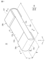
- FIG. 1 is an external perspective view showing a multi-layer ceramic capacitor which is an example of a multi-layer ceramic capacitor according to a first embodiment of the present invention
- 1 is a front view showing a multi-layer ceramic capacitor which is an example of a multi-layer ceramic capacitor according to a first embodiment of the present invention
- 1 is a left side view showing a multilayer ceramic capacitor which is an example of a multilayer ceramic capacitor according to a first embodiment of the present invention
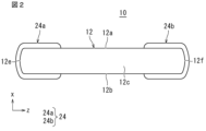
- FIG. 2 is a cross-sectional view taken along line IV-IV in FIG. 2 is a cross-sectional view taken along line VV in FIG. 1.
- FIG. 1 is a schematic cross-sectional view illustrating a structure around an end face of a laminate of a multilayer ceramic capacitor that is an example of the multilayer ceramic capacitor according to a first embodiment of the present invention.
- FIG. FIG. 11 is an external perspective view showing a multi-layer ceramic capacitor which is an example of a multi-layer ceramic capacitor according to a second embodiment of the present invention.
- 8 is a cross-sectional view taken along line VIII-VIII in FIG. 7.
- 9 is a cross-sectional view taken along line IX-IX in FIG. 7.
- 8 is a cross-sectional view taken along line XX in FIG. 7.
- FIG. 8 is an exploded perspective view of the laminate shown in FIG. 7 .
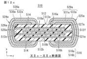
- FIG. 11 is a schematic cross-sectional view taken along line XIIa-XIIa in FIG. 10, illustrating the structure of a multilayer ceramic capacitor which is an example of a multilayer ceramic capacitor according to a second embodiment of the present invention.
- FIG. 12 is a schematic cross-sectional view taken along line XIIb-XIIb in FIG. 11, illustrating the structure of a multilayer ceramic capacitor which is an example of a multilayer ceramic capacitor according to a second embodiment of the present invention.
- FIG. FIG. 13 is a schematic cross-sectional view taken along line XIIIc-XIIIc in FIG. 11, illustrating the structure of a multilayer ceramic capacitor which is an example of a multilayer ceramic capacitor according to a second embodiment of the present invention.
- FIG. 12 is a schematic cross-sectional view taken along line XIId-XIId in FIG. 11, illustrating the structure of a multilayer ceramic capacitor which is an example of a multilayer ceramic capacitor according to a second embodiment of the present invention.
- FIG. 13 is a schematic cross-sectional view taken along line XIII-XIII in FIG. 11, illustrating the structure of a multilayer ceramic capacitor which is an example of a multilayer ceramic capacitor according to a second embodiment of the present invention.
- 8 is a cross-sectional view showing a modification of the line XX in FIG. 7.
- FIG. 8 is an exploded perspective view showing a modified example of the laminate shown in FIG. 7 .
- FIG. 10A is a schematic cross-sectional view illustrating a structure of an external electrode of a multilayer ceramic capacitor that is an example of a multilayer ceramic capacitor according to a modified example of a second embodiment of the present invention
- FIG. 10B is a schematic cross-sectional view illustrating a structure of an external electrode different from that of the multilayer ceramic capacitor of FIG. 1A
- FIG. 1B is a schematic cross-sectional view illustrating a structure of an external electrode of a multilayer ceramic capacitor which is an example of a multilayer ceramic capacitor according to another modified example of the second embodiment of the present invention
- FIG. 1B is a schematic cross-sectional view illustrating a structure of an external electrode different from that of the multilayer ceramic capacitor of FIG.
- FIG. 1A is a schematic cross-sectional view illustrating a structure of an external electrode of a multilayer ceramic capacitor which is an example of a multilayer ceramic capacitor according to another modified example of the second embodiment of the present invention
- FIG. 1B is a schematic cross-sectional view illustrating a structure of an external electrode different from that of the multilayer ceramic capacitor of FIG.
- FIG. 1 is an external perspective view showing a multilayer ceramic capacitor which is an example of the multilayer ceramic capacitor according to the first embodiment of the present invention.
- FIG. 2 is a front view showing a multilayer ceramic capacitor which is an example of the multilayer ceramic capacitor according to the first embodiment of the present invention.
- FIG. 3 is a top view showing a multilayer ceramic capacitor which is an example of the multilayer ceramic capacitor according to the first embodiment of the present invention.
- FIG. 4 is a left side view showing a multilayer ceramic capacitor which is an example of the multilayer ceramic capacitor according to the first embodiment of the present invention.
- FIG. 1 is an external perspective view showing a multilayer ceramic capacitor which is an example of the multilayer ceramic capacitor according to the first embodiment of the present invention.
- FIG. 2 is a front view showing a multilayer ceramic capacitor which is an example of the multilayer ceramic capacitor according to the first embodiment of the present invention.
- FIG. 3 is a top view showing a multilayer ceramic capacitor which is an example of the multilayer ceramic capacitor according to the first embodiment of
- FIG. 5 is a cross-sectional view taken along line V-V in FIG. 1.
- FIG. 6 is a cross-sectional schematic view for explaining a structure around an end face of a laminate of a multilayer ceramic capacitor which is an example of the multilayer ceramic capacitor according to the first embodiment of the present invention.
- the multilayer ceramic capacitor 10 has a laminate 12 and an external electrode 24. Below, the configuration of each will be explained in the order of the laminate 12 and the external electrode 24.
- the laminate 12 has a plurality of laminated dielectric layers 14 and a plurality of internal electrode layers 16. Furthermore, the laminate 12 includes a first main surface 12a and a second main surface 12b facing a height direction x, which is the stacking direction of the plurality of dielectric layers 14, a first side surface 12c and a second side surface 12d facing a width direction y perpendicular to the height direction x, and a first end surface 12e and a second end surface 12f facing a length direction z perpendicular to the height direction x and the width direction y.
- the corner portion refers to a portion where three adjacent surfaces of the laminate 12 intersect
- the ridge portion refers to a portion where two adjacent surfaces of the laminate 12 intersect.
- unevenness may be formed on a part or all of the first main surface 12a and the second main surface 12b, the first side surface 12c and the second side surface 12d, and the first end surface 12e and the second end surface 12f.
- the laminate 12 has an effective layer portion 15a in which multiple internal electrode layers 16 face each other in the height direction x connecting the first main surface 12a and the second main surface 12b, a first outer layer portion 15b1 formed from multiple dielectric layers 14 located between the internal electrode layer 16 located closest to the first main surface 12a and the first main surface 12a, and a second outer layer portion 15b2 formed from multiple dielectric layers 14 located between the internal electrode layer 16 located closest to the second main surface 12b and the second main surface 12b.
- the first outer layer 15b1 is located on the first main surface 12a side of the laminate 12, and is an assembly of multiple dielectric layers 14 located between the first main surface 12a and the internal electrode layer 16 closest to the first main surface 12a.
- the second outer layer 15b2 is located on the second main surface 12b side of the laminate 12, and is an assembly of multiple dielectric layers 14 located between the second main surface 12b and the internal electrode layer 16 closest to the second main surface 12b.
- the area sandwiched between the first outer layer 15b1 and the second outer layer 15b2 is the effective layer 15a.
- the number of dielectric layers 14 to be stacked is not particularly limited, but is preferably 10 to 2000, including the first outer layer 15b1 and the second outer layer 15b2.
- the thickness of the dielectric layers 14 is preferably 10 ⁇ m or less.
- the dielectric layer 14 may be formed from, for example, a dielectric material.
- the dielectric material may be, for example, a dielectric ceramic composed of a main component such as BaTiO3 , CaTiO3 , SrTiO3 , or CaZnO3 .
- a material containing a subcomponent such as a Mn compound, an Fe compound, a Cr compound, a Co compound, or a Ni compound added to the main component may also be used.
- the dielectric layer 14 may have a plurality of crystal grains including a perovskite type compound having a basic structure of BaTiO 3 .
- the crystal grain size is preferably 1 ⁇ m or less.
- the size of the crystal grains is designed appropriately according to the thickness of the dielectric layer 14.
- the thickness of the first outer layer 15b1 is preferably 1 ⁇ m or more and 15 ⁇ m or less.
- the thickness of the second outer layer 15b2 is preferably 1 ⁇ m or more and 15 ⁇ m or less.
- the thickness of the first outer layer 15b1 is defined by measuring the distance between the first main surface 12a and either the first internal electrode layer 16a or the second internal electrode layer 16b of the internal electrode layer 16 closest to the first main surface 12a.
- the thickness of the second outer layer 15b2 is defined by measuring the distance between the second main surface 12b and either the first internal electrode layer 16a or the second internal electrode layer 16b of the internal electrode layer 16 closest to the second main surface 12b.
- the first end face 12e of the laminate 12 is preferably curved from the first main surface 12a to the second main surface 12b.
- the second end face 12f of the laminate 12 is preferably curved from the first main surface 12a to the second main surface 12b. This increases the exposed area on the first end face 12e and the second end face 12f of the internal electrode layer 16, thereby increasing the adhesive strength between the conductive component of the external electrode 24 and the laminate 12. In addition, since the exposed area of the conductive component of the external electrode 24 is increased, an increase in ESR is suppressed.
- the radius of curvature of the curved first end surface 12e is preferably 5/2 or less of the thickness dimension in the height direction x of the laminate 12 at the center in the length direction z of the laminate 12.
- the radius of curvature of the curved second end surface 12f is preferably 5/2 or less of the thickness dimension in the height direction x of the laminate 12 at the center in the length direction z of the laminate 12.
- the radius of curvature is 5/2 or more, so the exposed area of the internal electrode layer 16 is reduced, so the adhesion area between the conductive component in the external electrode 24 and the internal electrode layer 16 is reduced, and the adhesion strength between the external electrode 24 and the laminate 12 is reduced. In addition, it becomes difficult to sufficiently reduce the ESR.
- the radius of curvature of the first end face 12e and the second end face 12f of the laminate 12 can be measured by the following measurement method.
- the cross section of the multilayer ceramic capacitor 10 is exposed. Specifically, polishing is performed until the position of 1/2W of the multilayer ceramic capacitor 10 is reached so that it is approximately parallel to the first side surface 12c or the second side surface 12d. Next, for example, a microscope (VHX-5000: manufactured by Keyence Corporation) is used to magnify 1500 times, and the dimension in the height direction x connecting the first main surface 12a and the second main surface 12b on the polished cross section of the laminate 12 is measured.
- VHX-5000 manufactured by Keyence Corporation
- position O where the dimension in the length direction of the first end face 12e is maximum. It is then defined as position P1 where a perpendicular line (a straight line along the height direction x) V1 passing through the end 18b1 of the second opposing electrode portion 18b of the second internal electrode layer 16b that is not exposed on the first end face 12e side among the multiple electrode layers of the internal electrode layer 16 intersects with the surface on the first main surface 12a side of the laminate 12, and position P2 where the perpendicular line V1 intersects with the surface on the second main surface 12b side of the laminate 12.
- position Q1 is defined as the intersection point between a perpendicular line V2 passing through a position shifted from position P1 by a distance d, which is 5% of the distance D, toward the first end face 12e side of the laminate 12 and the surface on the first main surface 12a side of the laminate 12
- position Q2 is defined as the intersection point between a perpendicular line V2 passing through a position shifted from position P2 by a distance d toward the first end face 12e side of the laminate 12 and the surface on the second main surface 12b side of the laminate 12.
- the radius of curvature of the contour portion R of the cross section passing through position O is measured starting from positions Q1 and Q2, and this is taken as the radius of curvature of the first end face 12e.
- position O' where the dimension in the length direction z of the second end face 12f is maximum.
- position Q1' is defined as the intersection point between a perpendicular line passing through a position shifted by a distance d', which is 5% of the distance D between position P1' and position O' along the width direction y, toward the second end face 12f, and the surface on the first main surface 12a side of the laminate 12
- position Q2' is defined as the intersection point between a perpendicular line passing through a position shifted by a distance d' from position P2' toward the second end face 12f, and the surface on the second main surface 12b side of the laminate 12.
- the radius of curvature of the contour portion R' of the cross section passing through position O' is measured starting from each of the extreme positions Q1' and Q2', and this is taken as the radius of curvature of the second end face 12f.
- positions P1 and P2 are measured based on the position of the end portion 18b1 of the second internal electrode layer 16b that is closest to the first end face 12e, as indicated by the symbol, and positions Q1 and Q2, which are the starting points for measuring the radius of curvature, are defined.
- the thickness of the laminate 12 in the height direction x is preferably 60 ⁇ m or less. When the thickness is 60 ⁇ m or less, the above-mentioned effects of the present invention can be obtained.
- first side surface 12c is preferably curved from the first main surface 12a to the second main surface 12b.
- the second side surface 12d is preferably curved from the first main surface 12a to the second main surface 12b. This prevents the laminate 12 from chipping.
- the internal electrode layer 16 includes a first internal electrode layer 16a and a second internal electrode layer 16b.
- the first internal electrode layer 16a and the second internal electrode layer 16b are alternately stacked with the dielectric layer 14 interposed therebetween.
- the first internal electrode layer 16a is disposed on the surface of the dielectric layer 14.
- the first internal electrode layer 16a has a first opposing electrode portion 18a that faces the second internal electrode layer 16b, and a first lead electrode portion 20a that is located on one end side of the first internal electrode layer 16a and extends from the first opposing electrode portion 18a to the first end face 12e of the laminate 12. The end of the first lead electrode portion 20a is led out to the first end face 12e and exposed.
- the shape of the first opposing electrode portion 18a of the first internal electrode layer 16a is not particularly limited, but is preferably rectangular in plan view. However, the corners in plan view may be rounded or may be formed at an angle in plan view (tapered). It may also be tapered in plan view, with a slope in either direction.
- the shape of the first extraction electrode portion 20a of the first internal electrode layer 16a is not particularly limited, but is preferably rectangular in plan view. However, the corners in plan view may be rounded or may be formed at an angle in plan view (tapered). It may also be tapered in plan view, with a slope in either direction.
- the width of the first opposing electrode portion 18a of the first internal electrode layer 16a and the width of the first extraction electrode portion 20a of the first internal electrode layer 16a may be formed to be the same width, or one of them may be formed to be narrower in width.
- the second internal electrode layer 16b is disposed on a surface of a dielectric layer 14 different from the dielectric layer 14 on which the first internal electrode layer 16a is disposed. It has a second opposing electrode portion 18b that faces the first internal electrode layer 16a, and a second extraction electrode portion 20b that is located on one end side of the second internal electrode layer 16b and extends from the second opposing electrode portion 18b to the second end face 12f of the laminate 12. The end of the second extraction electrode portion 20b is extended to the second end face 12f and exposed.
- the shape of the second opposing electrode portion 18b of the second internal electrode layer 16b is not particularly limited, but is preferably rectangular in plan view. However, the corners in plan view may be rounded or may be formed at an angle in plan view (tapered). It may also be tapered in plan view, with a slope in either direction.
- the shape of the second extraction electrode portion 20b of the second internal electrode layer 16b is not particularly limited, but is preferably rectangular in plan view. However, the corners in plan view may be rounded or may be formed at an angle in plan view (tapered). It may also be tapered in plan view, with a slope in either direction.
- the width of the second opposing electrode portion 18b of the second internal electrode layer 16b and the width of the second extraction electrode portion 20b of the second internal electrode layer 16b may be formed to be the same width, or one of them may be formed to be narrower in width.
- the first extraction electrode portion 20a of the first internal electrode layer 16a may be curved toward the center of the first end face 12e of the laminate 12.
- the second extraction electrode portion 20b of the second internal electrode layer 16b may be curved toward the center of the second end face 12f of the laminate 12.
- the distance between the first extraction electrode portion 20a of the first internal electrode layer 16a that is drawn out to the first end face 12e and the one that is closest to the first main surface 12a and the one that is closest to the second main surface 12b may be shorter than the distance between the first opposing electrode portion 18a of the first internal electrode layer 16a that is closest to the first main surface 12a and the one that is closest to the second main surface 12b.
- the distance between the second extraction electrode portion 20b of the second internal electrode layer 16b that is drawn out to the second end surface 12f and the one that is closest to the first main surface 12a and the one that is closest to the second main surface 12b may be shorter than the distance between the second opposing electrode portion 18b of the second internal electrode layer 16b that is closest to the first main surface 12a and the one that is closest to the second main surface 12b.
- the laminate 12 includes ends (hereinafter referred to as "L gaps") 22b of the laminate 12 formed between the end of the first internal electrode layer 16a opposite the first lead electrode portion 20a and the second end face 12f, and between the end of the second internal electrode layer 16b opposite the second lead electrode portion 20b and the first end face 12e.
- the laminate 12 includes a side portion (hereinafter referred to as a "W gap") 22a of the laminate 12 formed between one end in the width direction y of the first opposing electrode portion 18a and the second opposing electrode portion 18b and the first side surface 12c, and between the other end in the width direction y of the first opposing electrode portion 18a and the second opposing electrode portion 18b and the second side surface 12d.
- a W gap a side portion of the laminate 12 formed between one end in the width direction y of the first opposing electrode portion 18a and the second opposing electrode portion 18b and the first side surface 12c
- a step layer may be disposed in the L gap 22b.
- the first internal electrode layer 16a or the second internal electrode layer 16b may be arranged so as to cover a portion of the step layer, or the step layer may be arranged so as to cover a portion of the first internal electrode layer 16a or the second internal electrode layer 16b.
- the step layer has a thickness similar to that of the dielectric layer 14.
- the step layer is preferably made of the same components as the dielectric layer 14, but is not limited to this.
- a first dummy electrode layer and a second dummy electrode layer may be disposed in the L gap 22b.
- the first dummy electrode layer and the second dummy electrode layer may be disposed on the first outer layer portion 15b1 and the second outer layer portion 15b2. In this case, it is preferable that they are disposed on the portion corresponding to the location obtained by translating the L gap 22b in the height direction x.
- the first dummy electrode layer preferably has a thickness similar to the sum of the thicknesses of the first internal electrode layers 16a. In other words, the first dummy electrode layer preferably has a thickness similar to the thickness of the first internal electrode layers 16a multiplied by the number of first internal electrode layers 16a.
- the first internal electrode layer 16a and the second internal electrode layer 16b can be made of an appropriate conductive material, for example, metals such as Ni, Cu, Ag, Pd, Au, or alloys containing at least one of these metals, such as an Ag-Pd alloy.
- the first opposing electrode portion 18a of the first internal electrode layer 16a and the second opposing electrode portion 18b of the second internal electrode layer 16b face each other via the dielectric layer 14, forming a capacitance and exhibiting the characteristics of a capacitor.
- the area of each of the first internal electrode layer 16a and the second internal electrode layer 16b of the internal electrode layer 16 must be increased, so it is preferable that the LW surface coverage of each of the first internal electrode layer 16a and the second internal electrode layer 16b is 90% or more.
- the LW surface coverage is defined as the ratio of the area inside the edge of the first internal electrode layer 16a or the second internal electrode layer 16b when viewed from the LW surface (the plane formed by the length direction z and the width direction y) of the laminate 12 minus the area of the gap.
- each of the first internal electrode layer 16a and the second internal electrode layer 16b has a uniform thickness, but the thickness of the edge portion in the width direction y may be greater than the thickness of the center portion in the width direction y.
- the thickness of the first internal electrode layer 16a and the second internal electrode layer 16b is preferably, for example, about 0.2 ⁇ m or more and 2.0 ⁇ m or less.
- first internal electrode layers 16a and second internal electrode layers 16b is 10 or more and 2000 or less.
- external electrodes 24 are disposed on the first end face 12e side and the second end face 12f side of the laminate 12.
- the external electrode 24 includes a base electrode layer 26 and a plating layer 28 formed to cover the base electrode layer 26.
- the external electrode 24 has a first external electrode 24a and a second external electrode 24b.
- the first external electrode 24a is disposed only on the surface of the first end face 12e of the laminate 12, a portion of the first main face 12a, and a portion of the second main face 12b. In this case, the first external electrode 24a is electrically connected to the first extraction electrode portion 20a of the first internal electrode layer 16a.
- the first external electrode 24a is not disposed on a portion of the first side face 12c and a portion of the second side face 12d, but may extend around slightly.
- the second external electrode 24b is disposed only on the surface of the second end face 12f of the laminate 12, a portion of the first main face 12a, and a portion of the second main face 12b. In this case, the second external electrode 24b is electrically connected to the second extraction electrode portion 20b of the second internal electrode layer 16b.
- the second external electrode 24b is not disposed on a portion of the first side face 12c and a portion of the second side face 12d, but may extend around slightly.
- the thickness of the first external electrode 24a and the second external electrode 24b is, for example, approximately 1 ⁇ m or more and 30.0 ⁇ m or less.
- the base electrode layer 26 includes a first base electrode layer 26a and a second base electrode layer 26b.
- the first base electrode layer 26a is formed to cover the first end face 12e of the laminate 12, a portion of the first main surface 12a on the side of the first end face 12e of the laminate 12, and a portion of the second main surface 12b on the side of the first end face 12e of the laminate 12.
- the second base electrode layer 26b is formed to cover the second end face 12f of the laminate 12, as well as a portion of the first main surface 12a on the side of the second end face 12f of the laminate 12, and a portion of the second main surface 12b on the side of the second end face 12f of the laminate 12.
- the base electrode layer 26 formed from a thin film layer includes at least one selected from a baked layer, a conductive resin layer, a thin film layer, etc.
- the baking layer includes a glass component and a metal component.
- the glass component of the baking layer includes at least one selected from B, Si, Ba, Mg, Al, Li, etc.
- the metal component of the baking layer includes at least one selected from Cu, Ni, Ag, Pd, Ag-Pd alloy, Au, etc.
- the baking layer is formed by applying a conductive paste including a glass component and a metal component to the laminate 12 and baking it.
- the baked layer may be formed by simultaneously baking a laminated chip having an internal electrode layer 16 and a dielectric layer 14 with a conductive paste applied to the laminated chip, or may be formed by baking a laminated chip having an internal electrode layer 16 and a dielectric layer 14 to obtain a laminate, and then baking a conductive paste onto the laminate.
- the firing layer by firing a material to which a dielectric material has been added instead of a glass component.
- the baking layer may be multiple layers.
- the thickness of the first base electrode layer 26a located at the first end face 12e in the center in the height direction x is preferably, for example, 0.1 ⁇ m or more and 200 ⁇ m or less.
- the thickness of the second base electrode layer 26b located at the second end face 12f in the center in the height direction x is preferably, for example, 0.1 ⁇ m or more and 200 ⁇ m or less.
- the thickness of the first base electrode layer 26a located on the first principal surface 12a and the second principal surface 12b at the center in the height direction x is, for example, 0.1 ⁇ m or more and 200 ⁇ m or less.
- the thickness of the second base electrode layer 26b located on the first principal surface 12a and the second principal surface 12b at the center in the height direction x is, for example, 0.1 ⁇ m or more and 200 ⁇ m or less.
- the base electrode layer 26 as a conductive resin layer contains a thermosetting resin and a metal. Since the conductive resin layer contains a thermosetting resin, it is more flexible than a conductive layer made of, for example, a plating film or a fired product of a conductive paste. Therefore, even if the multilayer ceramic capacitor is subjected to a physical impact or an impact due to a thermal cycle, the conductive resin layer functions as a buffer layer and can prevent cracks in the multilayer ceramic capacitor.
- the metal contained in the conductive resin layer can be Ag, Cu, Ni or an alloy of these.
- Metal powder with an Ag-coated surface can also be used.
- metal powder with an Ag-coated surface it is preferable to use Cu or Ni as the metal powder.
- Cu that has been treated to prevent oxidation can also be used.
- the reason for using Ag conductive metal powder as the metal contained in the conductive resin layer is that Ag has the lowest resistivity of all metals, making it suitable as an electrode material, and because Ag is a precious metal, it does not oxidize and has high resistance.
- the reason for using Ag-coated metal is that it is possible to make the base metal cheaper while maintaining the above-mentioned properties of Ag.
- the metal contained in the conductive resin layer is preferably contained in an amount of 35 vol% or more and 75 vol% or less relative to the total volume of the conductive resin.
- the average particle size of the metal contained in the conductive resin layer is not particularly limited.
- the average particle size of the conductive filler may be, for example, about 0.3 ⁇ m or more and 10 ⁇ m or less.
- the metal contained in the conductive resin layer is mainly responsible for the electrical conductivity of the conductive resin layer. Specifically, when the conductive fillers come into contact with each other, an electrical path is formed inside the conductive resin layer.
- the metal contained in the conductive resin layer is not particularly limited, but may be spherical or flat, and it is preferable to use a mixture of spherical metal powder and flat metal powder.
- thermosetting resins such as epoxy resin, phenolic resin, urethane resin, silicone resin, polyimide resin, etc.
- epoxy resin which has excellent heat resistance, moisture resistance, adhesion, etc., is one of the most suitable resins.
- the resin contained in the conductive resin layer is preferably contained in an amount of 25 vol% or more and 65 vol% or less relative to the total volume of the conductive resin.
- the conductive resin layer preferably contains a curing agent in addition to the thermosetting resin.
- a curing agent in addition to the thermosetting resin.
- various known compounds such as phenol-based, amine-based, acid anhydride-based, and imidazole-based compounds can be used as the curing agent for the epoxy resin.
- the base electrode layer 26 as a conductive resin layer may be multiple layers.
- the conductive resin layer may be disposed on the baked layer so as to cover the baked layer, or may be disposed directly on the laminate.
- the thickness of the first base electrode layer 26a located at the first end face 12e in the center in the height direction x is preferably, for example, 10 ⁇ m or more and 200 ⁇ m or less.
- the thickness of the second base electrode layer 26b located at the second end face 12f in the center in the height direction x is preferably, for example, 10 ⁇ m or more and 200 ⁇ m or less.
- the thickness of the first base electrode layer 26a located on the first principal surface 12a and the second principal surface 12b at the center in the height direction x is, for example, 5 ⁇ m or more and 50 ⁇ m or less.
- the thickness of the second base electrode layer 26b located on the first principal surface 12a and the second principal surface 12b at the center in the height direction x is, for example, 5 ⁇ m or more and 50 ⁇ m or less.
- the base electrode layer 26 as a thin film layer is preferably formed by a thin film formation method such as sputtering or vapor deposition, etc.
- the thin film layer is preferably a layer of 1 ⁇ m or less in thickness in which metal particles are deposited.
- the plating layer 28 includes a first plating layer 28a and a second plating layer 28b.
- the first plating layer 28a is disposed so as to cover the first base electrode layer 26a.
- the second plating layer 28b is disposed so as to cover the second base electrode layer 26b.
- the plating layer 28 is formed from multiple layers.
- the plating layer 28 preferably contains at least one selected from, for example, Cu, Ni, Ag, Pd, Ag-Pd alloy, Au, etc.
- the plating layer 28 may be formed of multiple layers. In this embodiment, it has a two-layer structure of Ni plating and Sn plating, and includes a lower plating layer 30, which is a Ni plating layer that covers the base electrode layer 26, and an upper plating layer 32, which is a Sn plating layer that is arranged to cover the lower plating layer 30.
- the underlayer plating layer 30 has a first underlayer plating layer 30a and a second underlayer plating layer 30b.
- the first underlayer plating layer 30a is arranged so as to cover the surface of the first underlayer electrode layer 26a. Specifically, the first underlayer plating layer 30a is arranged on the first end face 12e of the surface of the first underlayer electrode layer 26a, and is provided so as to extend to the first main surface 12a and the second main surface 12b of the surface of the first underlayer electrode layer 26a.
- the second underlayer plating layer 30b is arranged so as to cover the surface of the second underlayer electrode layer 26b. Specifically, the second underlayer plating layer 30b is arranged on the first end face 12e of the surface of the second underlayer electrode layer 26b, and is provided so as to extend to the first main surface 12a and the second main surface 12b of the surface of the second underlayer electrode layer 26b.
- the upper plating layer 32 has a first upper plating layer 32a and a second upper plating layer 32b.
- the first upper plating layer 32a is disposed so as to cover the first lower plating layer 30a. Specifically, the first upper plating layer 32a is disposed on the first end face 12e of the surface of the first lower plating layer 30a, and is provided so as to extend to the first main surface 12a and the second main surface 12b of the surface of the first lower plating layer 30a.
- the second upper plating layer 32b is disposed so as to cover the second lower plating layer 30b. Specifically, the second upper plating layer 32b is disposed on the second end face 12f of the surface of the second lower plating layer 30b, and is provided so as to extend to the first main surface 12a and the second main surface 12b of the surface of the second lower plating layer 30b.
- the plating layer 28 has a three-layer structure, it is preferable that the layers are stacked in the order of Sn plating, Ni plating, and Sn plating.
- each plating layer is preferably 1 ⁇ m or more and 15 ⁇ m or less.
- the plating layer may be a direct plating layer formed directly on the surface of the laminate 12. That is, the multilayer ceramic capacitor 10 may have a structure including a direct plating layer electrically connected to the first internal electrode layer 16a or the second internal electrode layer 16b. In such a case, the direct plating layer may be formed after a catalyst is disposed on the surface of the laminate 12 as a pretreatment.
- the direct plating layer preferably contains at least one metal selected from, for example, Cu, Ni, Sn, Pb, Au, Ag, Pd, Bi, or Zn, or an alloy containing such a metal.
- the direct plating layer be formed using Cu, which has good bonding properties with Ni.
- each direct plating layer is preferably 1 ⁇ m or more and 15 ⁇ m or less.
- the metal ratio per unit volume of the plating layer is preferably 99 volume % or more.
- the dimension in the length direction z of the multilayer ceramic capacitor 10 including the laminate 12, the first external electrode 24a, and the second external electrode 24b is defined as dimension L
- the dimension in the height direction x of the multilayer ceramic capacitor 10 including the laminate 12, the first external electrode 24a, and the second external electrode 24b is defined as dimension T
- the dimension in the width direction y of the multilayer ceramic capacitor 10 including the laminate 12, the first external electrode 24a, and the second external electrode 24b is defined as dimension W.
- the dimensions of the multilayer ceramic capacitor 10 are preferably such that the L dimension in the length direction z is 0.2 mm or more and 6.5 mm or less, the T dimension in the height direction x is 0.03 mm or more and 6.5 mm or less, and the W dimension in the width direction y is 0.1 mm or more and 5.5 mm or less.
- the ESL can be reduced by reversing the L dimension and the W dimension to shorten the current path.
- each of a first end face 12 e and a second end face 12 f of the laminate 12 is curved from the first main surface 12 a to the second main surface 12 b, and the radius of curvature is 5/2 or less of the thickness dimension in the height direction x of the laminate 12 at the center part in the longitudinal direction z of the laminate 12.
- This increases the exposed area on the first end face 12e and the second end face 12f of the internal electrode layer 16, thereby increasing the adhesive strength between the conductive component of the external electrode 24 and the laminate 12.
- the ESR can be kept small.
- first side surface 12c and the second side surface 12d of the laminate 12 are each curved from the first main surface 12a to the second main surface 12b, it is possible to prevent the laminate 12 from cracking.
- a dielectric sheet and a conductive paste for the internal electrodes are prepared.
- the dielectric sheet and the conductive paste for the internal electrode layers contain a binder (e.g., a known organic binder) and a solvent (e.g., a known organic binder).
- a binder e.g., a known organic binder
- a solvent e.g., a known organic binder
- a conductive paste for the internal electrodes is printed in a predetermined pattern on the dielectric sheet, for example by screen printing or gravure printing, to form an internal electrode pattern.
- a conductive paste layer is formed by applying a paste made of a conductive material onto the dielectric sheet by a method such as the printing method described above.
- the paste made of a conductive material is, for example, a metal powder to which an organic binder and an organic solvent have been added.
- an outer layer dielectric sheet on which no internal electrode pattern is printed is also produced.
- the laminated sheet is produced using the dielectric sheets on which these internal electrode patterns are formed. That is, a predetermined number of dielectric sheets for outer layers on which no internal electrode patterns are formed are laminated, and dielectric sheets on which internal electrode patterns corresponding to the first internal electrode layer 16a and dielectric sheets on which internal electrode patterns corresponding to the second internal electrode layer 16b are formed are alternately laminated on top of the dielectric sheets, and a predetermined number of dielectric sheets for outer layers on which no internal electrode patterns are formed are further laminated on top of the dielectric sheets to produce the laminated sheet.
- the laminated sheets are pressed in the lamination direction using a means such as a hydrostatic press to create a laminated block.
- the laminated block is cut to the specified size and laminated chips are cut out.
- a laminated chip having a desired shape is formed by barrel polishing.
- the diameter of the media for barrel polishing is preferably in the range of 0.2 mm to 0.7 mm
- the amount of media is preferably in the range of 200 cc to 700 cc
- the media is rotated not only in one direction but in multiple directions. In this manner, barrel polishing is performed until the entire end face of the laminated chip is rounded as desired.
- the firing temperature depends on the materials of the dielectric layers and the internal electrode layers, but is preferably 900°C or higher and 1400°C or lower.
- a base electrode layer 26 is formed on the first end face 12e and the second end face 12f of the laminate 12, as well as on a portion of the first principal surface 12a and a portion of the second principal surface 12b.
- a conductive paste that will serve as a base electrode layer is applied to the first end face 12e and the second end face 12f of the laminate 12, as well as a portion of the first main surface 12a and a portion of the second main surface 12b of the laminate 12, to form the first base electrode layer 26a and the second base electrode layer 26b of the base electrode layer 26.
- a conductive paste containing a glass component and a metal is applied, for example by dipping, and then a baking process is performed.
- the temperature of the baking process is preferably 700°C or higher and 900°C or lower.
- the surface of the baked layer is plated.
- the conductive resin layer may be formed on the surface of the baked layer, or the conductive resin layer may be formed directly on the laminate without forming a baked layer.
- the conductive resin layer is formed by applying a conductive resin paste containing a thermosetting resin and a metal component onto the baked layer or laminate, and then carrying out a heat treatment at a temperature of 250°C to 550°C to thermally cure the resin and form a conductive resin layer.
- the atmosphere during this heat treatment is preferably an N2 atmosphere.
- the base electrode layer 26 formed as a thin film layer is a layer of 1 ⁇ m or less in which metal particles are deposited.
- a plating layer may be directly provided on the exposed portions of the internal electrode layers 16 of the laminate 12. In this case, the following method is used.
- Either electrolytic plating or electroless plating may be used for plating, but electroless plating has the disadvantage that it requires pretreatment with a catalyst or the like to improve the plating deposition rate, which complicates the process. Therefore, it is usually preferable to use electrolytic plating.
- As a plating method it is preferable to use barrel plating.
- an upper layer plating electrode may be formed on the surface of the lower layer plating electrode in a similar manner.
- a plating layer 28 is formed on the surface of the base electrode layer 26.
- a lower plating layer 30, which is a Ni plating layer, and an upper plating layer 32, which is a Sn plating layer arranged so as to cover the lower plating layer 30, are formed on the base electrode layer 26 as a baked layer.
- the Ni plating layer and the Sn plating layer are formed in sequence, for example, by barrel plating.
- the multilayer ceramic capacitor 10 shown in Figure 1 can be manufactured.
- the method for manufacturing a multilayer ceramic capacitor according to the present embodiment described above can improve the adhesive strength between the conductive components of the external electrodes and the internal electrodes, and can reduce the ESR, making it possible to manufacture a high-quality multilayer ceramic capacitor according to the present invention that has high moisture resistance and reliability.
- FIG. 7 is an external perspective view showing a multilayer ceramic capacitor which is an example of the multilayer ceramic capacitor according to the second embodiment of the present invention.
- FIG. 8 is a cross-sectional view taken along line VIII-VIII in FIG. 7.
- FIG. 9 is a cross-sectional view taken along line IX-IX in FIG. 7.
- FIG. 10 is a cross-sectional view taken along line XX in FIG. 7.
- FIG. 11 is an exploded perspective view of the laminate shown in FIG. 7.
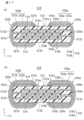
- FIG. 12a is a cross-sectional schematic view taken along line XIIa-XIIa in FIG. 10, and is a cross-sectional schematic view for explaining the structure of a multilayer ceramic capacitor which is an example of the multilayer ceramic capacitor according to the second embodiment of the present invention.
- FIG. 12b is a schematic cross-sectional view taken along line XIIb-XIIb in FIG. 10, and is a schematic cross-sectional view for explaining the structure of a multilayer ceramic capacitor that is an example of a multilayer ceramic capacitor according to the second embodiment of the present invention.
- FIG. 12c is a schematic cross-sectional view taken along line XIIc-XIIc in FIG. 10, and is a schematic cross-sectional view for explaining the structure of a multilayer ceramic capacitor that is an example of a multilayer ceramic capacitor according to the second embodiment of the present invention.
- FIG. 12d is a schematic cross-sectional view taken along line XIId-XIId in FIG.
- FIG. 10 is a schematic cross-sectional view for explaining the structure of an external electrode of a multilayer ceramic capacitor that is an example of a multilayer ceramic capacitor according to the second embodiment of the present invention.
- FIG. 13 is a schematic cross-sectional view taken along line XIII-XIII in FIG. 10, and is a schematic cross-sectional view for explaining the structure of a multilayer ceramic capacitor that is an example of a multilayer ceramic capacitor according to the second embodiment of the present invention.
- the multilayer ceramic capacitor 510 includes a laminate 512 and external electrodes 524, 525.
- the laminate 512 includes a plurality of dielectric layers 514 and a plurality of internal electrode layers 516.
- the laminate 512 has a first main surface 512a and a second main surface 512b that face each other in a height direction x, a first side surface 512c and a second side surface 512d that face each other in a width direction y perpendicular to the height direction x, and a third side surface 512e and a fourth side surface 512f that face each other in a length direction z perpendicular to the height direction x and the width direction y.
- the first main surface 512a and the second main surface 512b extend along the width direction y and the length direction z, respectively.
- the first side surface 512c and the second side surface 512d extend along the height direction x and the width direction z, respectively.
- the third side surface 512e and the fourth side surface 512f extend along the height direction x and the width direction y, respectively. Therefore, the height direction x is the direction connecting the first main surface 512a and the second main surface 512b, the width direction y is the direction connecting the first side surface 512c and the second side surface 512d, and the length direction z is the direction connecting the third side surface 512e and the fourth side surface 512f.
- the laminate 512 has a rectangular parallelepiped shape.
- the corners are the portions where three faces of the laminate 512 intersect, and the ridges are the portions where two faces of the laminate 512 intersect.
- the laminate 512 has an effective layer portion 515a in which multiple internal electrode layers 516 face each other in the height direction x connecting the first main surface 512a and the second main surface 512b, a first outer layer portion 515b1 formed from multiple dielectric layers 514 located between the internal electrode layer 516 located closest to the first main surface 512a and the first main surface 512a, and a second outer layer portion 515b2 formed from multiple dielectric layers 514 located between the internal electrode layer 516 located closest to the second main surface 512b and the second main surface 512b.
- the first outer layer 515b1 is located on the first main surface 512a side of the laminate 512, and is an assembly of multiple dielectric layers 514 located between the first main surface 512a and the internal electrode layer 516 closest to the first main surface 512a.
- the second outer layer 515b2 is located on the second main surface 512b side of the laminate 512, and is an assembly of multiple dielectric layers 514 located between the second main surface 512b and the internal electrode layer 516 closest to the second main surface 512b.
- the area sandwiched between the first outer layer portion 515b1 and the second outer layer portion 515b2 is the effective layer portion 515a.
- the area sandwiched between the first outer layer portion 515b1 and the second outer layer portion 515b2 is the effective layer portion 515a.
- the number of dielectric layers 514 to be stacked is not particularly limited, but is preferably 50 or less, including the first outer layer portion 515b1 and the second outer layer portion 515b2.
- the thickness of the dielectric layers 514 is preferably 0.2 ⁇ m or more and 10.0 ⁇ m or less.
- the area sandwiched between the first outer layer 515b1 and the second outer layer 515b2 is the effective layer 515a.
- the effective layer 515a is the area where the internal electrode layers 516 are stacked.
- the dielectric layer 514 can be formed of, for example, a dielectric material.
- the dielectric material can be a dielectric ceramic mainly composed of BaTiO3 , CaTiO3 , SrTiO3 , CaZnO3 , or the like.
- a subcomponent such as a Mn compound, an Fe compound, a Cr compound, a Co compound, or a Ni compound, the content of which is less than that of the main component, can be added to the main component.
- the dielectric layer 514 may have a plurality of crystal grains including a perovskite type compound having a basic structure of BaTiO 3. Since the thinner the dielectric layer 514 is, the greater the capacitance of the capacitor is, the more preferable the crystal grain size is 1 ⁇ m or less.
- the dielectric layer 514 for the active layer portion 515a is composed of dielectric ceramic particles with a perovskite structure, the main component of which is a perovskite compound containing, for example, Ba and Ti.
- At least one of Si, Mg, Ba, and Mn may be added as an additive to these main components.
- the additive is present between the ceramic particles.
- the dielectric layer 514 for the first outer layer portion 515b1 and the second outer layer portion 515b2 is formed from the same dielectric ceramic material as the dielectric layer 514 for the active layer portion 515a. Note that the dielectric layer 514 for the first outer layer portion 515b1 and the second outer layer portion 515b2 may be formed from a material different from that of the dielectric layer 514 for the active layer portion 515a.
- the dielectric layers 514 for the first outer layer portion 515b1 and the second outer layer portion 515b2 each have a multi-layer structure
- each of the dielectric layers 514 for the first outer layer portion 515b1 and the second outer layer portion 515b2 may be a multiple laminated layer or a single layer structure.
- Each of the first side surface 512c, the second side surface 512d, the third side surface 512e, and the fourth side surface 512f is curved from the first main surface 512a to the second main surface 512b.
- the first major surface 512a is preferably curved across each of the first side surface 512c, the second side surface 512d, the third side surface 512e and the fourth side surface 512f.
- the second main surface 512b is preferably curved across each of the first side surface 512c, the second side surface 512d, the third side surface 512e, and the fourth side surface 512f.
- Each of the first side 512c, the second side 512d, the third side 512e, and the fourth side 512f is curved from the first main surface 12a to the second main surface 12b, and it is preferable that the radius of curvature is 5/2 or less of the thickness dimension in the height direction x of the laminate 12 at the center in the length direction z of the laminate 12.
- a silane coupling agent layer may be provided on the surface of the laminate 512. Also, it is preferable that the silane coupling agent is provided on at least one of the first main surface 512a and the second main surface 512b. More preferably, the silane coupling agent may be disposed on both the first main surface 512a and the second main surface 512b. Also, the silane coupling agent may be disposed on the first side surface 512c and the second side surface 512d. In this case, it is preferable that the silane coupling agent is disposed on a part or the entirety of the portion of the first side surface 512c and the second side surface 512d where the first external electrode 524a and the second external electrode 524b are not disposed.
- silane coupling agent layer By providing a silane coupling agent layer, it is possible to prevent the intrusion of moisture, flux, and the like from the outside into the laminate 512. Therefore, when mounting the flux, it is possible to suppress corrosion caused by the organic acid contained in the flux, and therefore to suppress a decrease in moisture resistance reliability.
- the silane coupling agent layer is preferably made of a fluorine-based silane coupling agent or a carbon-based silane coupling agent.
- the fluorine-based silane coupling agent contained in the silane coupling agent layer is CF 3 -(CF 2 ) n1 -R-Si(O-R') 3 (wherein n1 is an integer of 0 or more, R is a substituent containing Si or O or an alkylene group, and R' is an alkyl group).
- n1 may be an integer of 0 or more and 7 or less.
- R' may be a methyl group or an ethyl group.
- the silane coupling agent has at least one alkoxy group, which is a reactive group.
- the silane coupling agent also has one or more perfluoroalkyl groups.
- fluorine-based silane coupling agents include: CF 3 (CF 2 ) 5 (CH 2 ) 2 Si(OCH 3 ) 3 , CF 3 (CF 2 ) 3 (CH 2 ) 2 Si(OCH 3 ) 3 , CF 3 (CF 2 ) 3 (CH 2 ) 2 Si(OC 2 H 5 ) 3 , CF 3 (CF 2 ) 7 (CH 2 ) 2 Si(OCH 3 ) 3 , CF3CH2O ( CH2 ) 15Si ( OCH3 ) 3 , CF3 ( CH2 ) 2Si ( CH3 ) 2 ( CH2 ) 15Si ( OCH3 ) 3 , CF 3 (CF 2 ) 3 (CH 2 ) 2 Si(CH 3 ) 2 (CH 2 ) 9 Si(OCH 3 ) 3 , CF3COO ( CH2 ) 15Si ( OCH3 ) 3 , CF 3 (CF 2 ) 5 (CH 2 ) 2 Si(OC 2 H 5 )
- the carbon-based silane coupling agent contained in the silane coupling agent layer is A silane coupling agent represented by the formula (RO) 3 Si--(CH 2 ) n2 --CH 3 (wherein n2 is an integer of 0 to 17, and R is a methyl group or an ethyl group) is preferred.
- Examples of the carbon-based silane coupling agent that can be used include Shin-Etsu Chemical's KBM-3103C (decyltrimethoxysilane), KBM-13 (methyltrimethoxysilane), KBE-13 (methyltriethoxysilane), KBM-3033 (n-propyltrimethoxysilane), KBE-3033 (n-propyltriethoxysilane), KBM-3063 (hexyltrimethoxysilane), KBE-3063 (hexyltriethoxysilane), and Tokyo Chemical Industry Co., Ltd. (TCI): octadecyltrimethoxysilane.
- carbon-based silane coupling agents that can be used include the following: Shin-Etsu Chemical: KBM-103 (phenylmethoxysilane), KBM-3066 (1,6-bis(trimethoxysilyl)hexane), KBM-9659 (tris-(trimethoxysilylpropyl)isocyanurate)
- the internal electrode layer 516 has a plurality of first internal electrode layers 516a and a plurality of second internal electrode layers 516b.
- the first internal electrode layers 516a and the second internal electrode layers 516b are alternately laminated in a direction connecting the first main surface 512a and the second main surface 512b with the dielectric layer 514 interposed therebetween.
- the first internal electrode layer 516a is disposed on the surface of the dielectric layer 514.
- the first internal electrode layer 516a faces the first main surface 512a and the second main surface 512b, has a first opposing electrode portion 518a facing the second internal electrode layer 516b, and is laminated in the direction connecting the first main surface 512a and the second main surface 512b.
- the second internal electrode layer 516b is disposed on a surface of a dielectric layer 514 different from the dielectric layer 514 on which the first internal electrode layer 516a is disposed.
- the second internal electrode layer 516b has a second opposing electrode portion 518b that faces the first main surface 512a and the second main surface 512b, and is laminated in the direction connecting the first main surface 512a and the second main surface 512b.
- the first internal electrode layer 516a is drawn out to the first side 512c and the third side 512e of the laminate 512 by the first drawn out electrode portion 520a, and is drawn out to the second side 512d and the fourth side 512f of the laminate 512 by the second drawn out electrode portion 520b.
- the width of the first drawn out electrode portion 520a drawn out to the first side 512c may be approximately equal to the width of the first drawn out electrode portion 520a drawn out to the third side 512e
- the width of the second drawn out electrode portion 520b drawn out to the second side 512d may be approximately equal to the width of the second drawn out electrode portion 520b drawn out to the fourth side 512f.
- the first extraction electrode portion 520a is extracted to the first side surface 512c of the laminate 512
- the second extraction electrode portion 520b is extracted to the second side surface 512d of the laminate 512.
- the second internal electrode layer 516b is drawn out to the first side 512c and the fourth side 512f of the laminate 512 by the third drawing electrode portion 521a, and drawn out to the second side 512d and the third side 512e of the laminate 512 by the fourth drawing electrode portion 521b.
- the width of the third drawing electrode portion 521a drawn out to the first side 512c may be approximately equal to the width of the fourth drawing electrode portion 521b drawn out to the second side 512d may be approximately equal to the width of the fourth drawing electrode portion 521b drawn out to the third side 512e.
- the third extraction electrode portion 521a is extracted to the fourth side surface 512f side of the laminate 512
- the fourth extraction electrode portion 521b is extracted to the third side surface 512e side of the laminate 512.
- a straight line connecting the first extraction electrode portion 520a and the second extraction electrode portion 520b of the first internal electrode layer 516a intersects with a straight line connecting the third extraction electrode portion 521a and the fourth extraction electrode portion 521b of the second internal electrode layer 516b.
- the first extraction electrode portion 520a of the first internal electrode layer 516a and the fourth extraction electrode portion 521b of the second internal electrode layer 516b are preferably drawn out to opposing positions, and the second extraction electrode portion 520b of the first internal electrode layer 516a and the third extraction electrode portion 521a of the second internal electrode layer 516b are preferably drawn out to opposing positions.
- the first extraction electrode portion 520a may be configured to extract the first internal electrode layer 516a only to the first side surface 512c of the laminate 512
- the second extraction electrode portion 520b may be configured to extract the first internal electrode layer 516a only to the second side surface 512d of the laminate 512.
- the third extraction electrode portion 521a may be configured to extract the first internal electrode layer 516a only to the fourth side surface 512f of the laminate 512
- the fourth extraction electrode portion 521b may be configured to extract the first internal electrode layer 516a only to the third side surface 512e of the laminate 512.
- the laminate 512 includes an end (L gap) 522b of the laminate 512 formed between one end in the length direction z of the first opposing electrode portion 518a and the third side surface 512e, and between the other end in the length direction z of the second opposing electrode portion 518b and the fourth side surface 512f.
- the laminate 512 includes a side portion (W gap) 522a of the laminate 512 formed between one end in the width direction y of the first opposing electrode portion 518a and the first side surface 512c, and between the other end in the width direction y of the second opposing electrode portion 518b and the second side surface 512d.
- the dielectric layer 514 for the active layer portion 515a may be disposed so as to be sandwiched between the first internal electrode layer 516a and the first internal electrode layer 516a.
- the first internal electrode layer 516a and the first internal electrode layer 516a are disposed continuously via the dielectric layer 514 for the active layer portion 515a.
- the dielectric layer 514 for the active layer portion 515a may be disposed so as to be sandwiched between the second internal electrode layer 516b and the second internal electrode layer 516b.
- the second internal electrode layer 516b and the second internal electrode layer 516b are disposed continuously via the dielectric layer 514 for the active layer portion 515a.
- the shape of the first opposing electrode portion 518a of the first internal electrode layer 516a is not particularly limited, but is preferably rectangular in plan view. However, the corners in plan view may be rounded or may be formed at an angle in plan view (tapered). It may also be tapered in plan view, with a slope in either direction.
- the shape of the first lead electrode portion 520a and the second lead electrode portion 520b of the first internal electrode layer 516a is not particularly limited, but is preferably rectangular in plan view. However, the corners in plan view may be rounded or may be formed at an angle in plan view (tapered). Also, the shape may be tapered in plan view with a slope in either direction.
- the shape of the second opposing electrode portion 518b of the second internal electrode layer 516b is not particularly limited, but is preferably rectangular in plan view. However, the corners in plan view may be rounded or may be formed at an angle in plan view (tapered). It may also be tapered in plan view, with an incline in either direction.
- the shape of the third extraction electrode portion 521a and the fourth extraction electrode portion 521b of the second internal electrode layer 16b is not particularly limited, but is preferably rectangular in plan view. However, the corners in plan view may be rounded or may be formed at an angle in plan view (tapered). Also, they may be tapered in plan view with a slope in either direction.
- the material of the internal electrode layer 516 can be, for example, a metal such as Ni, Cu, Ag, Pd, or Au, or an appropriate conductive material that includes one of these metals, such as an Ag-Pd alloy, but is not limited to this.
- the number of layers of the first internal electrode layer 516a and the second internal electrode layer 516b can be changed as appropriate depending on the size, etc. Increasing the number of first internal electrode layers 516a can prevent the DC resistance from increasing.
- the first internal electrode layers 516a may be stacked continuously in the height direction x, or the first internal electrode layers 516a and the second internal electrode layers 516b may be stacked alternately.
- a first dummy electrode layer may be disposed on an extension line in the height direction x of the first extraction electrode portion 520a of the first internal electrode layer 516a.
- a second dummy electrode layer may be arranged on an extension line of the second lead electrode portion 520b of the first internal electrode layer 516a in the height direction x.
- a third dummy electrode layer may be arranged on an extension line in the height direction x of the third extraction electrode portion 521a of the second internal electrode layer 516b.
- a fourth dummy electrode layer may be arranged on an extension line in the height direction x of the fourth extraction electrode portion 521b of the second internal electrode layer 516b.
- the first dummy electrode layer and the second dummy electrode layer may be disposed on the first outer layer portion 515b1 and the second outer layer portion 515b2.
- the first dummy electrode layer is preferably disposed on the same plane as the second internal electrode layer 516b and has the same thickness as the second internal electrode layer 516b. In this case, the first dummy electrode layer and the second internal electrode layer 516b are not electrically connected.
- the second dummy electrode layer is preferably disposed on the same plane as the second internal electrode layer 516b and has the same thickness as the second internal electrode layer 516b. At this time, the second dummy electrode layer and the second internal electrode layer 516b are not electrically connected.
- the third dummy electrode layer is preferably disposed on the same plane as the first internal electrode layer 516a and has the same thickness as the first internal electrode layer 516a. In this case, the third dummy electrode layer and the first internal electrode layer 516a are not electrically connected.
- the fourth dummy electrode layer is preferably disposed on the same plane as the first internal electrode layer 516a and has the same thickness as the first internal electrode layer 516a. In this case, the fourth dummy electrode layer and the first internal electrode layer 516a are not electrically connected.
- the current path can be shortened.
- it can be used as the starting point for plating when forming the direct plating layer described later, so a uniform plating film can be formed.
- the first and second extraction electrode portions 520a and 520b of the first internal electrode layer 516a may be curved.
- the third extraction electrode portion 521a and the fourth extraction electrode portion 521b of the second internal electrode layer 516b may be curved.
- the first main surface 512a or the second main surface 512b may be curved.
- the mounting surface may be curved to shorten the current path.
- the distance between the first internal electrode layer 516a extending to the first side 512c and the third side 512e, and the second side 512d and the fourth side 512f, which is located closest to the first main surface 512a, and the one located closest to the second main surface 512b, may be shorter than the distance between the first opposing electrode portion 518a of the first internal electrode layer 516a, which is located closest to the first main surface 512a, and the one located closest to the second main surface 512b.
- the distance between the one of the second internal electrode layers 516b extending to the second side 512d and the fourth side 512f and the first side 512c and the third side 512e that is closest to the first main surface 512a and the one that is closest to the second main surface 512b may be shorter than the distance between the one of the second opposing electrode portions 518b of the second internal electrode layer 516b that is closest to the first main surface 512a and the one that is closest to the second main surface 512b.
- the area of each of the first internal electrode layer 516a and the second internal electrode layer 516b of the internal electrode layer 516 must be increased, so it is preferable that the LW surface coverage of each of the first internal electrode layer 16a and the second internal electrode layer 16b is 90% or more.
- the LW surface coverage is defined as the ratio of the area inside the edge of the first internal electrode layer 516a or the second internal electrode layer 516b when viewed from the LW surface of the laminate 512 minus the area of the gap.
- the first internal electrode layer 516a has a uniform thickness, but the edge portion of the first internal electrode layer 516a may be thicker than the center portion. By making the edge portion thicker than the center portion, the coverage is improved, the current path is shortened, and the ESL characteristics are improved.
- the edge of the first internal electrode layer 516a may be thinner than the center. By making the edge thinner than the center, the step corresponding to the thickness of the first internal electrode layer 516a is mitigated, suppressing structural defects.
- the second internal electrode layer 516b preferably has a uniform thickness, but the edge portion of the second internal electrode layer 516b may be thicker than the center portion. By making the edge portion thicker than the center portion, the coverage is improved, the current path is shortened, and the ESL characteristics are improved.
- the thickness of the edge portion of the second internal electrode layer 516b may be greater than the thickness of the central portion.
- the thickness of the edge portion of the second internal electrode layer 516b may be less than the thickness of the central portion.
- each of the first internal electrode layer 516a and the second internal electrode layer 516b of the internal electrode layer 516 is preferably, for example, about 0.1 ⁇ m or more and 0.8 ⁇ m or less.
- the total number of first internal electrode layers 516a and second internal electrode layers 516b of the internal electrode layer 516 is preferably about 20 to 60.
- external electrodes 524, 525 are disposed on the laminate 512.
- the thickness of the external electrodes 524, 525 is preferably, for example, about 1 ⁇ m or more and 30.0 ⁇ m or less.
- the external electrode 524 includes a base electrode layer 526 and a plating layer 528 formed to cover the base electrode layer 526.
- the external electrode 525 includes a base electrode layer 527 and a plating layer 529 formed to cover the base electrode layer 527.
- the external electrode 524 has a first external electrode 524a and a second external electrode 524b.
- the first external electrode 524a is arranged so as to cover the first extraction electrode portion 520a on the first side surface 512c and the third side surface 512e, and is arranged so as to cover a part of the first main surface 512a and the second main surface 512b.
- the first external electrode 524a is electrically connected to the first extraction electrode portion 520a of the first internal electrode layer 516a.
- the first external electrode 524a may be arranged to cover the first extraction electrode portion 520a only on the first side surface 512c.
- the second external electrode 524b is arranged so as to cover the second extraction electrode portion 520b on the second side surface 512d and the fourth side surface 512f, and is arranged so as to cover a part of the first main surface 512a and the second main surface 512b.
- the second external electrode 524b is electrically connected to the second extraction electrode portion 520b of the first internal electrode layer 516a.
- the second external electrode 524b may be arranged to cover the second extraction electrode portion 520b only on the second side surface 512d.
- the external electrode 525 has a third external electrode 525a and a fourth external electrode 525b.
- the third external electrode 525a is arranged so as to cover the third extraction electrode portion 521a on the first side surface 512c and the fourth side surface 512f, and is arranged so as to cover a part of the first main surface 512a and the second main surface 512b.
- the third external electrode 525a is electrically connected to the third extraction electrode portion 521a of the second internal electrode layer 516b.
- the third external electrode 525a may be arranged to cover the third extraction electrode portion 521a only on the fourth side surface 512f.
- the fourth external electrode 525b is arranged so as to cover the fourth extraction electrode portion 521b on the second side surface 512d and the third side surface 512e, and is arranged so as to cover a part of the first main surface 512a and the second main surface 512b.
- the fourth external electrode 525b is electrically connected to the fourth extraction electrode portion 521b of the second internal electrode layer 516b.
- the fourth external electrode 525b may be arranged to cover the fourth extraction electrode portion 521b only on the third side surface 512e.
- the first opposing electrode portion 518a of the first internal electrode layer 516a and the second opposing electrode portion 518b of the second internal electrode layer 516b face each other via the dielectric layer 514, forming a capacitance. Therefore, a capacitance can be obtained between the first external electrode 524a and the second external electrode 524b to which the first internal electrode layer 516a is connected, and the third external electrode 525a and the fourth external electrode 525b to which the second internal electrode layer 516b is connected, and the characteristics of a capacitor are expressed.
- the base electrode layer 526 includes a first base electrode layer 526a and a second base electrode layer 526b.
- the first base electrode layer 526a is arranged so as to cover the first extraction electrode portion 520a on the first side surface 512c and the third side surface 512e, and is arranged so as to cover a portion of the first principal surface 512a and the second principal surface 512b.
- the second base electrode layer 526b is arranged so as to cover the second extraction electrode portion 520b on the second side surface 512d and the fourth side surface 512f, and is arranged so as to cover a portion of the first principal surface 512a and the second principal surface 512b.
- the base electrode layer 527 has a third base electrode layer 527a and a fourth base electrode layer 527b.
- the third base electrode layer 527a is arranged so as to cover the third extraction electrode portion 521a on the first side surface 512c and the fourth side surface 512f, and is arranged so as to cover parts of the first principal surface 512a and the second principal surface 512b.
- the fourth base electrode layer 527b is arranged so as to cover the fourth extraction electrode portion 521b on the second side surface 512d and the third side surface 512e, and is arranged so as to cover a portion of the first principal surface 512a and the second principal surface 512b.
- the first underlying electrode layer 526a, the second underlying electrode layer 526b, the third underlying electrode layer 527a, and the fourth underlying electrode layer 527b each include at least one selected from a baked layer, a thin film layer, a fired electrode layer, etc.
- the base electrode layer 526 as a baking layer contains a glass component and a metal.
- the glass component contains at least one element selected from the group consisting of B, Si, Ba, Mg, Al, Li, and the like.
- the metal of the baked layer includes, for example, at least one selected from Cu, Ni, Ag, Pd, Ag-Pd alloy, AU, etc.
- the baking layer may be multiple layers.
- the baked layer is formed by applying a conductive paste containing glass and metal to the laminate and baking it. It may be baked simultaneously with the internal electrode layer 516 or may be baked after the internal electrode layer 516 is baked.
- the thickness of the first base electrode layer 526a located on the first side 512c and the third side 512e at the center in the height direction x is preferably, for example, 1 ⁇ m or more and 11 ⁇ m or less. Also, the thickness of the second base electrode layer 526b located on the second side 512d and the fourth side 512f at the center in the height direction x is preferably 1 ⁇ m or more and 11 ⁇ m or less.
- the thickness of the first base electrode layer 526a located on the first principal surface 512a and the second principal surface 512b at the center in the height direction x is, for example, 1 ⁇ m or more and 11 ⁇ m or less.
- the thickness of the second base electrode layer 526b located on the first principal surface 12a and the second principal surface 12b at the center in the height direction x is, for example, 1 ⁇ m or more and 11 ⁇ m or less.
- the thickness at the center in the height direction x of the third base electrode layer 527a located on the first side 512c and the fourth side 512f is preferably, for example, 1 ⁇ m or more and 11 ⁇ m or less. Furthermore, the thickness at the center in the height direction x of the fourth base electrode layer 527b located on the second side 512d and the third side 512e is preferably 1 ⁇ m or more and 11 ⁇ m or less.
- the thickness of the third base electrode layer 527a located on the first principal surface 512a and the second principal surface 512b at the center in the height direction x is, for example, 1 ⁇ m or more and 11 ⁇ m or less.
- the thickness of the fourth base electrode layer 527b located on the first principal surface 12a and the second principal surface 12b at the center in the height direction x is, for example, 1 ⁇ m or more and 11 ⁇ m or less.
- the base electrode layers 526, 527 formed by thin film layers are preferably formed by a thin film formation method such as a sputtering method or a vapor deposition method.
- the base electrode layers 526, 527 formed by thin film layers are preferably sputter electrodes formed by a sputtering method.
- the thin film layers can be detected by, for example, a calibration curve method of the corresponding metal species using a fluorescent X-ray device.
- the thin film layers can also be detected from an actual observation image of a cross section of a component by FIB using a scanning microscope. The electrodes formed by the sputtering method will be described below.
- the base electrode layers 526 and 527 formed as thin film layers by the sputtering method are layers on which metal particles are deposited.
- the first base electrode layer 526a is located on a part of the first main surface 512a and the second main surface 512b, and is also located on a part of the corner where the first main surface 512a, the first side surface 512c, and the third side surface 512e intersect, and on a part of the corner where the second main surface 512b, the first side surface 512c, and the third side surface 512e intersect.
- it is preferably located from the first main surface 512a to 50% of the thickness of the first outer layer 515b1, and from the second main surface 512b to 50% of the thickness of the second outer layer 515b2.
- the second base electrode layer 526b is located on a part of the first main surface 512a and the second main surface 512b, and is located on a part of the corner where the first main surface 512a, the second side surface 512d, and the fourth side surface 512f intersect, and on a part of the corner where the second main surface 512b, the second side surface 512d, and the fourth side surface 512f intersect.
- it is preferably located from the first main surface 512a to 50% of the thickness of the first outer layer 515b1, and from the second main surface 512b to 50% of the thickness of the second outer layer 515b2.
- the third base electrode layer 527a is located on a part of the first main surface 512a and the second main surface 512b, and is located on a part of the corner where the first main surface 512a, the first side surface 512c, and the fourth side surface 512f intersect, and on a part of the corner where the second main surface 512b, the first side surface 512c, and the fourth side surface 512f intersect.
- it is preferably located from the first main surface 512a to 50% of the thickness of the first outer layer 515b1, and from the second main surface 512b to 50% of the thickness of the second outer layer 515b2.
- the fourth base electrode layer 527b is located on a part of the first main surface 512a and the second main surface 512b, and is located on a part of the corner where the first main surface 512a, the second side surface 512d, and the third side surface 512e intersect, and on a part of the corner where the second main surface 512b, the second side surface 512d, and the third side surface 512e intersect.
- it is preferably located from the first main surface 512a to 50% of the thickness of the first outer layer 515b1, and from the second main surface 512b to 50% of the thickness of the second outer layer 515b2.
- thin film layers are only disposed on the first principal surface 512a and the second principal surface 512b, so if the outer layer is thick, the distance between the internal electrode layer 16 and the thin film layers, the base electrode layers 526 and 527, becomes large, and there is a risk that the direct plating layer described below will become dented.
- the thin film layer is disposed so that it extends around to part of the side surface, it can be formed to have a uniform thickness when the direct plating layer is disposed, making it possible to improve moisture resistance.
- the base electrode layers 526, 527 formed from thin film layers may be located only on the first main surface 512a.
- the shape of the external electrode is approximately L-shaped, so the dimension in the stacking direction can be made smaller by the thickness of the external electrode.
- the base electrode layers 526, 527 formed from thin film layers may be located only on a portion of the first main surface 512a and the second main surface 512b, and may not extend around the first side surface 512c, the second side surface 512d, the third side surface 512e, and the fourth side surface 512f.
- the base electrode layers 526 and 527 which are formed from thin film layers, have a thickness of 1 ⁇ m or less in the height direction x connecting the first main surface 512a and the second main surface 512b.
- the base electrode layers 526 and 527 formed by firing the electrode layers are layers containing a metal component and a dielectric material that is the same component as the dielectric layer 14 .
- the base electrode layers 526, 527 formed by the fired electrode layers are disposed on the first principal surface 512a and the second principal surface 512b, as well as the first side surface 512c, the second side surface 512d, the third side surface 512e, and the fourth side surface 512f, and may be fired simultaneously with the laminate 512, or may be subjected to a firing process after firing the laminate 512.
- the first base electrode layer 526a is located only on a portion of the first main surface 512a and the second main surface 512b, and is arranged so as not to wrap around either the first side surface 512c or the third side surface 512e.
- the second base electrode layer 526b is located only on a portion of the first main surface 512a and the second main surface 512b, and is arranged so as not to wrap around either the second side surface 512d or the fourth side surface 512f.
- the third base electrode layer 527a is located only on a portion of the first main surface 512a and the second main surface 512b, and is arranged so as not to wrap around either the first side surface 512c or the fourth side surface 512f.
- the fourth base electrode layer 527b is located only on a portion of the first main surface 512a and the second main surface 512b, and is arranged so as not to wrap around either the second side surface 512d or the third side surface 512e.
- the base electrode layers 526, 527 formed from the fired electrode layers may be located only on the first main surface 512a.
- the shape of the external electrode is approximately L-shaped, so the dimension in the stacking direction can be made smaller by the thickness of the external electrode.
- the base electrode layers 526, 527 formed by the sintered electrode layer using the screen printing method may be located on a portion of the first main surface 512a and the second main surface 512b, and may also extend around the first side surface 512c, the second side surface 512d, the third side surface 512e, and the fourth side surface 512f.
- the base electrode layer 526 formed of the fired electrode layer may be disposed separately on the first principal surface 512a, the second principal surface 512b, and the side surface, as shown in FIG. 18(a).
- the base electrode layer 527 formed of the fired electrode layer may be disposed separately on the first principal surface 512a, the second principal surface 512b, and the side surface, as shown in FIG.
- the base electrode layers 526, 527 formed of fired electrode layers may be arranged discontinuously.
- discontinuous means that the first base electrode layer 526a of the base electrode layer 526 is in a state in which smearing occurs on the first main surface 512a, the second main surface 512b, the first side surface 512c, and the third side surface 512e, and that the second base electrode layer 526b of the base electrode layer 526 is in a state in which smearing occurs on the first main surface 512a, the second main surface 512b, the first side surface 512c, and the fourth side surface 512f.
- the third base electrode layer 527a of the base electrode layer 527 is in a state where smearing occurs on the first main surface 512a, the second main surface 512b, the second side surface 512d, and the third side surface 512e
- the fourth base electrode layer 527b of the base electrode layer 527 is in a state where smearing occurs on the first main surface 512a, the second main surface 512b, the second side surface 512d, and the fourth side surface 512f.
- the surface area of the conductive component increases, improving the adhesion of the direct plating layer described below.
- the base electrode layers 526, 527 formed by fired electrode layers arranged on the first principal surface 512a and the second principal surface 512b may be arranged over parts of the first side surface 512c, the second side surface 512d, the third side surface 512e, and the fourth side surface 512f as appropriate.
- the plating layer 528 includes a first plating layer 528a and a second plating layer 528b.
- the first plating layer 528a is disposed so as to cover the first base electrode layer 526a.
- the second plating layer 528b is disposed so as to cover the second base electrode layer 526b.
- the plating layer 529 includes a third plating layer 529a and a fourth plating layer 529b.
- the third plating layer 529a is disposed so as to cover the third base electrode layer 527a.
- the fourth plating layer 529b is arranged to cover the fourth base electrode layer 527b.
- the plating layer 528 contains, for example, at least one selected from Cu, Ni, Ag, Pd, an Ag-Pd alloy, Au, etc.
- the plating layer 529 contains at least one selected from, for example, Cu, Ni, Ag, Pd, an Ag-Pd alloy, Au, etc.
- the plating layer 528 may be formed of multiple layers. In this embodiment, it has a two-layer structure of Ni plating and Sn plating, and includes a lower plating layer 530 which is a Ni plating layer that covers the base electrode layer 526, and an upper plating layer 532 which is a Sn plating layer that is arranged to cover the lower plating layer 530. Similarly, the plating layer 529 includes a lower plating layer 531 and an upper plating layer 533 that is arranged to cover the base electrode layer 527 and the lower plating layer 531.
- the Ni plating layer prevents the base electrode layers 526, 527 from being eroded by solder when mounting the multilayer ceramic capacitor, and the Sn plating improves the wettability of the solder when mounting the multilayer ceramic capacitor, making mounting easier.
- the plating layers 528 and 529 have a three-layer structure, it is preferable that they are laminated in the order of Sn plating, Ni plating, and Sn plating.
- the underlayer plating layer 530 has a first underlayer plating layer 530a and a second underlayer plating layer 530b.
- the first underlayer plating layer 530a is disposed on the surface of the laminate 512 so as to cover the first underlayer electrode layer 526a disposed on the first principal surface 512a, the second principal surface 512b, the first side surface 512c, and the third side surface 512e.
- the second underlayer plating layer 530b is disposed on the surface of the laminate 512 so as to cover the second underlayer electrode layer 526b exposed on the first main surface 512a, the second main surface 512b, the second side surface 512d, and the fourth side surface 512f.
- the lower plating layer 531 has a third lower plating layer 531a and a fourth lower plating layer 531b.
- the third underlayer plating layer 531a is disposed on the surface of the laminate 512 so as to cover the third underlayer electrode layer 527ab exposed on the first main surface 512a, the second main surface 512b, the first side surface 512c, and the fourth side surface 512f.
- the fourth underlayer plating layer 531b is disposed on the surface of the laminate 512 so as to cover the fourth underlayer electrode layer 527b exposed on the first main surface 512a, the second main surface 512b, the second side surface 512d, and the third side surface 512e.
- the upper plating layer 532 has a first upper plating layer 532a and a second upper plating layer 532b.
- the first upper plating layer 532a is arranged so as to cover the first lower plating layer 530a. Specifically, the first upper plating layer 532a is arranged on the first side surface 512c and the third side surface 512e of the surface of the first lower plating layer 530a, and is provided so as to extend to the first main surface 512a and the second main surface 512b of the surface of the first lower plating layer 530a.
- the second upper plating layer 532b is disposed so as to cover the second lower plating layer 530b. Specifically, the second upper plating layer 532b is disposed on the second side surface 512d and the fourth side surface 512f of the surface of the second lower plating layer 530b, and is provided so as to extend to the first main surface 512a and the second main surface 512b of the surface of the second lower plating layer 530b.
- the upper plating layer 533 has a third upper plating layer 533a and a fourth upper plating layer 533b.
- the third upper plating layer 533a is disposed so as to cover the third lower plating layer 531a. Specifically, the third upper plating layer 533a is disposed on the first side surface 512c and the fourth side surface 512f of the surface of the third lower plating layer 531a, and is provided so as to extend to the first main surface 512a and the second main surface 512b of the surface of the third lower plating layer 531a.
- the fourth upper plating layer 533b is arranged so as to cover the fourth lower plating layer 531b. Specifically, the fourth upper plating layer 533b is arranged on the second side 512d and the third side 512e of the surface of the fourth lower plating layer 531b, and is provided so as to reach the first main surface 512a and the second main surface 512b of the surface of the fourth lower plating layer 531b.
- each of the plating layers 528 and 529 is preferably 1 ⁇ m or more and 11 ⁇ m or less.
- the plating layers 540, 541 may be formed directly between the base electrode layers 526, 527 and the plating layers 528, 529. That is, in the multilayer ceramic capacitor, the plating layers 540, 541 may be arranged so as to cover the base electrode layers 526, 527 on the main surfaces 512a, 512b, and may be arranged so as to be electrically connected to the first internal electrode layer 516a or the second internal electrode layer 516b on the side surfaces 512c, 512d. In such a case, the plating layers may be formed directly after a catalyst is provided on the surfaces of the base electrode layers 526, 527 and the laminate 512 as a pretreatment.
- 16(b) and 17(b) are examples in which plating layers 540, 541 are formed directly between the base electrode layers 526, 527 and the plating layers 528, 529. That is, the plating layers 540, 541 directly cover the base electrode layers 526, 527 on the main surfaces 512a, 512b side, and cover the internal electrode layer 516 on the side surfaces 521c, 512b side. Moreover, the direct plating layers 540, 541 shown in FIG. 18(b) cover the base electrode layers 526, 527 on the main surfaces 512a, 512b and the side surfaces 521c, 512b.
- the direct plating layer 540a is arranged so as to cover the first base electrode layer 526a arranged on the first principal surface 512a and the second principal surface 512b, and is arranged on the surface of the first side surface 512c so as to be electrically connected to the first internal electrode layer 516a exposed on at least the first side surface 512c.
- the direct plating layer 540b is arranged so as to cover the second base electrode layer 526b arranged on the first principal surface 512a and the second principal surface 512b, and is arranged on the surface of the second side surface 512d so as to be electrically connected to the first internal electrode layer 516a exposed at least on the second side surface 512d.
- the direct plating layer 541b is arranged so as to cover the third base electrode layer 527a arranged on the first principal surface 512a and the second principal surface 512b, and is arranged on the surface of the first side surface 512c so as to be electrically connected to the second internal electrode layer 516b exposed at least on the first side surface 512c.
- the direct plating layer 541a is arranged so as to cover the fourth base electrode layer 527b arranged on the first principal surface 512a and the second principal surface 512b, and is arranged on the surface of the second side surface 512d so as to be electrically connected to at least the second internal electrode layer 516b exposed on the second side surface 512d.
- the direct plating layer preferably contains at least one metal selected from, for example, Cu, Ni, Sn, Pb, Au, Ag, Pd, Bi, or Zn, or an alloy containing such a metal.
- the direct plating layer be formed using Cu, which has good bonding properties with Ni.
- each direct plating layer is preferably 1 ⁇ m or more and 11 ⁇ m or less.
- the metal ratio per unit volume of the direct plating layer is preferably 99 volume % or more.
- the first side surface 512c, the second side surface 512d, the third side surface 512e, and the fourth side surface 512f are each curved, so compared to when each side surface is flat, the exposed area of the internal electrode layer 16 is increased, and the time required for plating formation can be shortened. In addition, the probability of contact between the media and the metal component when forming the plating can be improved.
- the dimension in the length direction z of the multilayer ceramic capacitor 10 including the laminate 12 and the external electrodes 524, 525 is defined as the L dimension
- the dimension in the height direction x of the multilayer ceramic capacitor 10 including the laminate 12 and the external electrodes 524, 525 is defined as the T dimension
- the dimension in the width direction y of the multilayer ceramic capacitor 10 including the laminate 12 and the external electrodes 524, 525 is defined as the W dimension.
- the dimensions of the multilayer ceramic capacitor 10 are preferably such that the L dimension in the length direction z is 0.1 mm or more and 6.0 mm or less, the T dimension in the height direction x is 10 ⁇ m or more and 300 ⁇ m or less, and the W dimension in the width direction y is 0.1 mm or more and 6.0 mm or less.
- each of the first side surface 512c, the second side surface 512d, the third side surface 512e, and the fourth side surface 512f is curved from the first main surface 12a to the second main surface 12b.
- the radius of curvature is 5/2 or less of the thickness dimension in the height direction x of the laminate 12 at the center in the length direction z of the laminate 12.
- the radii of curvature of the first side 512c, the second side 512d, the third side 512e, and the fourth side 512f of the laminate 512 can be measured using the same measurement method as in the first embodiment.
- the radius of curvature of the first side surface 512c is based on the edge portions of the first opposing electrode portion 518a and the second opposing electrode portion 518b that are not extended to the first side surface 512c
- the radius of curvature of the second side surface 512d is based on the edge portions of the first opposing electrode portion 518a and the second opposing electrode portion 518b that are not extended to the second side surface 512d.
- the same standard is also used for the radii of curvature of the third side surface 512e and the fourth side surface 512f.
- the radius of curvature is defined starting from 5% into each side surface from each standard.
- the radius of curvature of the first side surface 512c is based on the edge portions of the first opposing electrode portion 518a and the second opposing electrode portion 518b on the first side surface 512c side
- the radius of curvature of the second side surface 512d is based on the edge portions of the first opposing electrode portion 518a and the second opposing electrode portion 518b on the second side surface 512d side.
- the radius of curvature is defined starting from 5% into each side surface from each reference point.
- a dielectric sheet and a conductive paste for the internal electrodes are prepared.
- the dielectric sheet and the conductive paste for the internal electrode layers contain a binder (e.g., a known organic binder) and a solvent (e.g., a known organic binder).
- a binder e.g., a known organic binder
- a solvent e.g., a known organic binder
- a conductive paste for the internal electrodes is printed in a predetermined pattern on the dielectric sheet, for example by screen printing or gravure printing, to form an internal electrode pattern.
- a conductive paste layer is formed by applying a paste made of a conductive material onto the dielectric sheet by a method such as the printing method described above.
- the paste made of a conductive material is, for example, a metal powder to which an organic binder and an organic solvent have been added.
- an outer layer dielectric sheet on which no internal electrode pattern is printed is also produced.
- a screen plate for printing the first internal electrode layer 516a and a screen plate for printing the second internal electrode layer 516b are prepared separately, and the internal electrode layers of the present invention can be printed using a printer capable of printing the two types of screen plates separately.
- the laminated sheet is produced using the dielectric sheets on which these internal electrode patterns are formed. That is, a predetermined number of dielectric sheets for the outer layer on which no internal electrode pattern is formed are laminated to form a portion that will become the first outer layer portion 515b1 on the first main surface 512a side.
- dielectric sheets on which an internal electrode pattern corresponding to the first internal electrode layer 516a is formed and dielectric sheets on which an internal electrode pattern corresponding to the second internal electrode layer 516b is formed are alternately laminated to form a portion that will become the effective layer portion 515a, and further on top of that, a predetermined number of dielectric sheets for the outer layer on which no internal electrode pattern is formed are laminated to form a portion that will become the second outer layer portion 515b2. In this way, the laminated sheet is produced.
- the laminated sheets are pressed in the lamination direction using a means such as a hydrostatic press to create a laminated block.
- the laminated block is cut to the specified size and laminated chips are cut out.
- the diameter of the media for barrel polishing is preferably in the range of 0.2 m to 0.7 m
- the amount of media is preferably in the range of 200 cc to 700 cc
- the media is rotated not only in one direction but in multiple directions. In this way, barrel polishing is performed until the entire end face of the laminated chip is rounded.
- the firing temperature depends on the ceramic and internal electrode materials, but is preferably 900°C or higher and 1400°C or lower.
- base electrode layers 526, 527 are formed on the first and second principal surfaces 512a, 512b, and on a portion of each of the first, second, 512d, third, 512e, and fourth side surfaces 512f of the laminate 512.
- a conductive paste that will serve as a base electrode layer is applied to a portion of each of the first side 512c, the second side 512d, the third side 512e, and the fourth side 512f of the laminate 512 to form a first base electrode layer 526a and a second base electrode layer 526b of the base electrode layer 526, and a third base electrode layer 527a and a fourth base electrode layer 527b of the base electrode layer 527.
- a conductive paste containing a glass component and a metal is applied by a method such as dipping, and then a baking process is performed to form the base electrode layer.
- the temperature of the baking process at this time is preferably 700°C or higher and 900°C or lower.
- the DIP method it is possible to form the coating not only on the first side surface 512c, the second side surface 512d, the third side surface 512e, and the fourth side surface 512f, which are the coating targets, but also on the first main surface 512a and the second main surface 512b, as well as on parts of these side surfaces or the side surfaces adjacent to the main surfaces.
- base electrode layer is a thin film layer
- masking or the like is performed, and base electrode layers 526 and 527 are formed by a thin film formation method such as sputtering or vapor deposition at the locations where external electrodes 524 and 525 are to be formed.
- the base electrode layers 526 and 527 are made of thin film layers, each of which is a layer of metal particles deposited to a thickness of 1 ⁇ m or less.
- the thin film layer is directly joined to a plating layer arranged so as to be joined to the internal electrode layer 16.
- a base electrode layer made of the fired electrode layer is arranged at desired positions on each of the first main surface 512a and the second main surface 512b, as well as the first side surface 512c, the second side surface 512d, the third side surface 512e, and the fourth side surface 512f by a screen printing method or the like, and then the laminated chip is fired.
- the firing temperature at this time is preferably 700°C or higher and 1400°C or lower.
- the base electrode layer which is a fired electrode layer
- the base electrode layer is preferably joined to a direct plating layer arranged so as to be joined to the internal electrode layer 16.
- the base electrode layer which is a fired electrode layer by screen printing
- the laminate 512 may be fired after the base electrode layer is arranged, or the baking process may be performed after firing the laminate 512.
- the plating layer may be formed on the surface of the base electrode layer, or directly on the laminate. More specifically, a Ni plating layer (base plating layer) and a Sn plating layer are formed on the base electrode layer. Either electrolytic plating or electroless plating may be used for plating.
- electroless plating has the disadvantage that pretreatment with a catalyst or the like is required to improve the plating deposition speed, which complicates the process. Therefore, it is usually preferable to use electrolytic plating.
- the multilayer ceramic capacitor 510 shown in Figure 7 can be manufactured.
- the method for manufacturing a multilayer ceramic capacitor according to the present embodiment described above can improve the adhesive strength between the conductive components of the external electrodes and the internal electrodes, and can reduce the ESR, making it possible to manufacture a high-quality multilayer ceramic capacitor according to the present invention that has high moisture resistance and reliability.
- Thickness of Ni plating layer Thickness of Ni plating layer at the center in the length direction of the Ni plating layer located on the first main surface and the second main surface, the first side surface and the second side surface: 3 ⁇ m
- Sn plating layer thickness thickness of the Sn plating layer at the center in the length direction of the Sn plating layer located on the first and second main surfaces, the first and second side surfaces: 3 ⁇ m
- ESR Test The ESR was measured by subjecting each sample of multilayer ceramic capacitor to a heat treatment in an air atmosphere at 150°C for 1 hour before the measurement, and then mounting the capacitor on a measurement board. After 24 ⁇ 2 hours from the completion of the heat treatment, the capacitor was measured using a network analyzer at a measurement frequency of 1 MHz. 100 capacitors were measured, and the average value was recorded as the value in the table. Note that, when sample number 1 was used as the standard, ⁇ : ESR is 97% or less of sample No. 1.-: ESR is greater than 97% of sample No. 1. The ESR was judged as good or bad based on the above.
- the radius of curvature is 5/2 or less of the thickness dimension in the height direction x of the laminate 12 at the center in the length direction z of the laminate 12, so good ESR measurement results of 97% or less were obtained compared to the ESR of sample No. 1.
- the radius of curvature is 5/2 or more of the thickness dimension in the height direction x of the laminate 12 at the center in the length direction z of the laminate 12, so the ESR measurement result was greater than 97% of the ESR of sample number 1.
- the first end face 12e and the second end face 12f of the laminate 12 are each curved from the first main surface 12a to the second main surface 12b, and the radius of curvature is 5/2 or less of the thickness dimension in the height direction x of the laminate 12 at the center in the length direction z of the laminate 12.
- This increases the exposed area of the first end face 12e and the second end face 12f of the internal electrode layer 16, thereby increasing the adhesive strength between the conductive component of the external electrode 24 and the laminate 12.
- the exposed area of the conductive component of the external electrode 24 is increased, the effect of suppressing the ESR to a low level was obtained.
- the first main surface 12a of the laminate 12 of the multilayer ceramic capacitor 10 may be curved from the first side surface 12c to the second side surface 12d, or may be curved from the first end surface 12e to the second end surface 12f.
- the second main surface 12b of the laminate 12 may be curved from the first side surface 12c to the second side surface 12d, or may be curved from the first end surface 12e to the second end surface 12f.
- the first main surface 512a of the laminate 512 of the multilayer ceramic capacitor 510 may be curved from the first side surface 512c to the second side surface 512d, or may be curved from the third side surface 512e to the fourth side surface 512f.
- the second main surface 512b of the laminate 512 may be curved from the first side surface 512c to the second side surface 512d, or may be curved from the third side surface 512e to the fourth side surface 512f.
- the insulating film includes a plurality of dielectric layers stacked together, the insulating film having a first main surface and a second main surface facing each other in a height direction which is a stacking direction of the dielectric layers, a first side surface and a second side surface facing each other in a width direction perpendicular to the height direction, a first end surface and a second end surface facing each other in a length direction perpendicular to the height direction and the width direction, a first internal electrode layer stacked alternately with the plurality of dielectric layers and exposed at the first end surface, and a second internal electrode layer stacked alternately with the plurality of dielectric layers and exposed at the second end surface;
- a laminate comprising: a first external electrode provided on the first end surface; a second external electrode provided on the second end surface, each of the first end surface and the second end surface is curved from the first main surface to the second main surface; a radius of curvature of each of the first end face and the second end face is 5/2 or less of a thickness
- a laminate comprising: a first external electrode connected to the first internal electrode layer; a second external electrode connected to the second internal electrode layer; The multilayer ceramic capacitor, wherein each of the first side surface, the second side surface, the third side surface, and the fourth side surface is curved from the first main surface to the second main surface.
- the first main surface is curved across each of the first side, the second side, the third side, and the fourth side;
- ⁇ 4> The multilayer ceramic capacitor according to ⁇ 2> or ⁇ 3>, wherein a radius of curvature of each of the first end face, the second end face, the third end face, and the fourth side face is 5/2 or less of a thickness in a height direction of the laminate at a central portion in a longitudinal direction of the laminate.
- ⁇ 5> The multilayer ceramic capacitor according to ⁇ 1>, wherein the thickness of the laminate in a height direction is 300 ⁇ m or less.
- ⁇ 6> The multilayer ceramic capacitor according to any one of ⁇ 2> to ⁇ 4>, wherein the thickness of the laminate in a height direction is 300 ⁇ m or less.
- the first external electrode is a first thin film layer disposed on the first major surface; a first direct plating layer disposed so as to be connected to the first internal electrode layer and covering a portion of the first thin film layer;
- the second external electrode is a second thin film layer disposed on the first major surface;
- ⁇ 8> The multilayer ceramic capacitor according to ⁇ 7>, wherein the thin film layer is arranged so as to wrap around from the first main surface to a portion of each of the first side surface, the second side surface, the third side surface, and the fourth side surface.
- the first external electrode is a first fired electrode layer comprising a metal component and a dielectric material disposed on the first major surface or the second major surface; a first base electrode layer arranged to be connected to the first internal electrode layer and covering a part of the first fired electrode layer;
- the second external electrode is a second fired electrode layer comprising a metal component and a dielectric material disposed on the first major surface or the second major surface;
- each of the first fired electrode layer and the second fired electrode layer is discontinuously disposed in the length direction or the width direction.
- each of the first fired electrode layer and the second fired electrode layer is disposed on the first side surface, the second side surface, the third side surface, and the fourth side surface.
- This invention relates to a multilayer ceramic capacitor, and in particular, can be used as a multilayer ceramic capacitor with external electrodes having a multilayer structure.
Landscapes
- Engineering & Computer Science (AREA)
- Power Engineering (AREA)
- Manufacturing & Machinery (AREA)
- Microelectronics & Electronic Packaging (AREA)
- Chemical & Material Sciences (AREA)
- Ceramic Engineering (AREA)
- Inorganic Chemistry (AREA)
- Materials Engineering (AREA)
- Fixed Capacitors And Capacitor Manufacturing Machines (AREA)
- Ceramic Capacitors (AREA)
Priority Applications (3)
| Application Number | Priority Date | Filing Date | Title |
|---|---|---|---|
| CN202380091361.9A CN120530466A (zh) | 2023-02-22 | 2023-12-14 | 层叠陶瓷电容器 |
| JP2025502122A JPWO2024176578A1 (https=) | 2023-02-22 | 2023-12-14 | |
| US19/215,440 US20250285808A1 (en) | 2023-02-22 | 2025-05-22 | Multilayer ceramic capacitor |
Applications Claiming Priority (2)
| Application Number | Priority Date | Filing Date | Title |
|---|---|---|---|
| JP2023025769 | 2023-02-22 | ||
| JP2023-025769 | 2023-02-22 |
Related Child Applications (1)
| Application Number | Title | Priority Date | Filing Date |
|---|---|---|---|
| US19/215,440 Continuation US20250285808A1 (en) | 2023-02-22 | 2025-05-22 | Multilayer ceramic capacitor |
Publications (1)
| Publication Number | Publication Date |
|---|---|
| WO2024176578A1 true WO2024176578A1 (ja) | 2024-08-29 |
Family
ID=92500964
Family Applications (1)
| Application Number | Title | Priority Date | Filing Date |
|---|---|---|---|
| PCT/JP2023/044761 Ceased WO2024176578A1 (ja) | 2023-02-22 | 2023-12-14 | 積層セラミックコンデンサ |
Country Status (4)
| Country | Link |
|---|---|
| US (1) | US20250285808A1 (https=) |
| JP (1) | JPWO2024176578A1 (https=) |
| CN (1) | CN120530466A (https=) |
| WO (1) | WO2024176578A1 (https=) |
Cited By (1)
| Publication number | Priority date | Publication date | Assignee | Title |
|---|---|---|---|---|
| WO2025115517A1 (ja) * | 2023-12-01 | 2025-06-05 | 京セラ株式会社 | 積層型電子部品 |
Citations (4)
| Publication number | Priority date | Publication date | Assignee | Title |
|---|---|---|---|---|
| JPH04263410A (ja) * | 1991-02-18 | 1992-09-18 | Taiyo Yuden Co Ltd | 電子部品及び外部電極用導電性ペ―ストの付着方法 |
| WO2017090530A1 (ja) * | 2015-11-27 | 2017-06-01 | 京セラ株式会社 | 積層型コンデンサおよびその実装構造体 |
| JP2019062100A (ja) * | 2017-09-27 | 2019-04-18 | 太陽誘電株式会社 | セラミック電子部品およびその製造方法 |
| JP2021174793A (ja) * | 2020-04-20 | 2021-11-01 | 株式会社村田製作所 | 積層セラミック電子部品 |
-
2023
- 2023-12-14 CN CN202380091361.9A patent/CN120530466A/zh active Pending
- 2023-12-14 JP JP2025502122A patent/JPWO2024176578A1/ja active Pending
- 2023-12-14 WO PCT/JP2023/044761 patent/WO2024176578A1/ja not_active Ceased
-
2025
- 2025-05-22 US US19/215,440 patent/US20250285808A1/en active Pending
Patent Citations (4)
| Publication number | Priority date | Publication date | Assignee | Title |
|---|---|---|---|---|
| JPH04263410A (ja) * | 1991-02-18 | 1992-09-18 | Taiyo Yuden Co Ltd | 電子部品及び外部電極用導電性ペ―ストの付着方法 |
| WO2017090530A1 (ja) * | 2015-11-27 | 2017-06-01 | 京セラ株式会社 | 積層型コンデンサおよびその実装構造体 |
| JP2019062100A (ja) * | 2017-09-27 | 2019-04-18 | 太陽誘電株式会社 | セラミック電子部品およびその製造方法 |
| JP2021174793A (ja) * | 2020-04-20 | 2021-11-01 | 株式会社村田製作所 | 積層セラミック電子部品 |
Cited By (4)
| Publication number | Priority date | Publication date | Assignee | Title |
|---|---|---|---|---|
| WO2025115517A1 (ja) * | 2023-12-01 | 2025-06-05 | 京セラ株式会社 | 積層型電子部品 |
| JPWO2025115517A1 (https=) * | 2023-12-01 | 2025-06-05 | ||
| US12573561B2 (en) | 2023-12-01 | 2026-03-10 | Kyocera Corporation | Multilayer electronic component |
| JP7829740B2 (ja) | 2023-12-01 | 2026-03-13 | 京セラ株式会社 | 積層型電子部品 |
Also Published As
| Publication number | Publication date |
|---|---|
| CN120530466A (zh) | 2025-08-22 |
| JPWO2024176578A1 (https=) | 2024-08-29 |
| US20250285808A1 (en) | 2025-09-11 |
Similar Documents
| Publication | Publication Date | Title |
|---|---|---|
| JP6806035B2 (ja) | 積層セラミックコンデンサ | |
| US10475584B2 (en) | Electronic component mount structure, electronic component, and method for manufacturing electronic component | |
| US11062848B2 (en) | Multilayer ceramic electronic component | |
| US20180174753A1 (en) | Multilayer ceramic capacitor | |
| JP2018088451A (ja) | 積層セラミックコンデンサ | |
| CN113539682B (zh) | 层叠陶瓷电子部件 | |
| US11495404B2 (en) | Multilayer ceramic electronic component | |
| JP2020202220A (ja) | 積層セラミック電子部品 | |
| JP2020088190A (ja) | 積層セラミック電子部品 | |
| JP2021034440A (ja) | 積層セラミック電子部品 | |
| JP2021034458A (ja) | 積層セラミック電子部品 | |
| JP2023013421A (ja) | 積層セラミック電子部品 | |
| JP2019212727A (ja) | 積層セラミックコンデンサおよび積層セラミックコンデンサの実装構造 | |
| US20250285808A1 (en) | Multilayer ceramic capacitor | |
| JP2020188081A (ja) | 積層セラミック電子部品 | |
| KR20250140456A (ko) | 적층 세라믹 콘덴서 | |
| JP2021125673A (ja) | 積層セラミックコンデンサ | |
| US12347621B2 (en) | Multilayer ceramic capacitor including main-surface-side outer layer portions including protective structures | |
| WO2025004486A1 (ja) | 積層セラミックコンデンサ | |
| JP7736197B2 (ja) | 積層セラミックコンデンサ | |
| US20250054703A1 (en) | Through-type multilayer ceramic capacitor | |
| WO2025004487A1 (ja) | 積層セラミックコンデンサ | |
| WO2025121052A1 (ja) | 電子部品の実装構造 | |
| JP2024068365A (ja) | 積層セラミック電子部品 | |
| CN121399707A (zh) | 层叠陶瓷电容器 |
Legal Events
| Date | Code | Title | Description |
|---|---|---|---|
| 121 | Ep: the epo has been informed by wipo that ep was designated in this application |
Ref document number: 23924222 Country of ref document: EP Kind code of ref document: A1 |
|
| WWE | Wipo information: entry into national phase |
Ref document number: 202380091361.9 Country of ref document: CN |
|
| ENP | Entry into the national phase |
Ref document number: 2025502122 Country of ref document: JP Kind code of ref document: A |
|
| WWE | Wipo information: entry into national phase |
Ref document number: 2025502122 Country of ref document: JP |
|
| WWP | Wipo information: published in national office |
Ref document number: 202380091361.9 Country of ref document: CN |
|
| NENP | Non-entry into the national phase |
Ref country code: DE |
|
| 122 | Ep: pct application non-entry in european phase |
Ref document number: 23924222 Country of ref document: EP Kind code of ref document: A1 |