WO2024176356A1 - 半導体水素圧力センサ及びその製造方法 - Google Patents
半導体水素圧力センサ及びその製造方法 Download PDFInfo
- Publication number
- WO2024176356A1 WO2024176356A1 PCT/JP2023/006252 JP2023006252W WO2024176356A1 WO 2024176356 A1 WO2024176356 A1 WO 2024176356A1 JP 2023006252 W JP2023006252 W JP 2023006252W WO 2024176356 A1 WO2024176356 A1 WO 2024176356A1
- Authority
- WO
- WIPO (PCT)
- Prior art keywords
- semiconductor
- pressure
- pressure sensor
- detection element
- protective film
- Prior art date
- Legal status (The legal status is an assumption and is not a legal conclusion. Google has not performed a legal analysis and makes no representation as to the accuracy of the status listed.)
- Ceased
Links
Images




Classifications
-
- G—PHYSICS
- G01—MEASURING; TESTING
- G01L—MEASURING FORCE, STRESS, TORQUE, WORK, MECHANICAL POWER, MECHANICAL EFFICIENCY, OR FLUID PRESSURE
- G01L19/00—Details of, or accessories for, apparatus for measuring steady or quasi-steady pressure of a fluent medium insofar as such details or accessories are not special to particular types of pressure gauges
- G01L19/06—Means for preventing overload or deleterious influence of the measured medium on the measuring device or vice versa
- G01L19/0627—Protection against aggressive medium in general
-
- G—PHYSICS
- G01—MEASURING; TESTING
- G01L—MEASURING FORCE, STRESS, TORQUE, WORK, MECHANICAL POWER, MECHANICAL EFFICIENCY, OR FLUID PRESSURE
- G01L19/00—Details of, or accessories for, apparatus for measuring steady or quasi-steady pressure of a fluent medium insofar as such details or accessories are not special to particular types of pressure gauges
- G01L19/06—Means for preventing overload or deleterious influence of the measured medium on the measuring device or vice versa
-
- G—PHYSICS
- G01—MEASURING; TESTING
- G01L—MEASURING FORCE, STRESS, TORQUE, WORK, MECHANICAL POWER, MECHANICAL EFFICIENCY, OR FLUID PRESSURE
- G01L19/00—Details of, or accessories for, apparatus for measuring steady or quasi-steady pressure of a fluent medium insofar as such details or accessories are not special to particular types of pressure gauges
- G01L19/0061—Electrical connection means
-
- G—PHYSICS
- G01—MEASURING; TESTING
- G01L—MEASURING FORCE, STRESS, TORQUE, WORK, MECHANICAL POWER, MECHANICAL EFFICIENCY, OR FLUID PRESSURE
- G01L19/00—Details of, or accessories for, apparatus for measuring steady or quasi-steady pressure of a fluent medium insofar as such details or accessories are not special to particular types of pressure gauges
- G01L19/0061—Electrical connection means
- G01L19/0069—Electrical connection means from the sensor to its support
-
- G—PHYSICS
- G01—MEASURING; TESTING
- G01L—MEASURING FORCE, STRESS, TORQUE, WORK, MECHANICAL POWER, MECHANICAL EFFICIENCY, OR FLUID PRESSURE
- G01L19/00—Details of, or accessories for, apparatus for measuring steady or quasi-steady pressure of a fluent medium insofar as such details or accessories are not special to particular types of pressure gauges
- G01L19/14—Housings
-
- G—PHYSICS
- G01—MEASURING; TESTING
- G01L—MEASURING FORCE, STRESS, TORQUE, WORK, MECHANICAL POWER, MECHANICAL EFFICIENCY, OR FLUID PRESSURE
- G01L9/00—Measuring steady of quasi-steady pressure of fluid or fluent solid material by electric or magnetic pressure-sensitive elements; Transmitting or indicating the displacement of mechanical pressure-sensitive elements, used to measure the steady or quasi-steady pressure of a fluid or fluent solid material, by electric or magnetic means
- G01L9/0041—Transmitting or indicating the displacement of flexible diaphragms
- G01L9/0042—Constructional details associated with semiconductive diaphragm sensors, e.g. etching, or constructional details of non-semiconductive diaphragms
Definitions
- This application relates to a semiconductor hydrogen pressure sensor and a method for manufacturing the same.
- the fuel cell system has an anode subsystem and a cathode subsystem.
- the anode subsystem supplies hydrogen, which is the fuel, to the fuel cell stack.
- the cathode subsystem supplies oxygen contained in the air to the fuel cell stack. The oxygen reacts with the fuel.
- the semiconductor hydrogen pressure sensor which measures the pressure of the medium, mainly hydrogen, that flows in and out of the fuel cell stack, is considered to be one of the key components that greatly affect the efficiency of the fuel cell system.
- the semiconductor hydrogen pressure sensor that measures the hydrogen pressure is required to have high hydrogen reliability as well as high precision pressure measurement, which is its original function.
- the semiconductor hydrogen pressure sensor needs to handle hydrogen with a purity of up to 100% in a maintenance-free state over the system's lifespan.
- the medium to be handled is, in principle, air.
- the medium containing hydrogen is the subject of pressure measurement due to cross leak phenomenon in the fuel cell stack, so the semiconductor hydrogen pressure sensor installed in the cathode subsystem is also required to be reliable with respect to hydrogen.
- the configuration of a conventional hydrogen pressure sensor that addresses these issues is described below.
- the pressure sensor is made of stainless steel or the like and is equipped with a metal pressure diaphragm that receives hydrogen pressure, an oil-filled section provided on the rear side of the metal pressure diaphragm, and a pressure detection element that detects the stress caused by the pressure received by the metal pressure diaphragm through the oil behind the oil-filled section and converts it into an electrical signal.
- Conventional pressure sensors use an indirect measurement method in which the pressure detection element detects the stress transmitted through the oil. The main reason for using the indirect measurement method is that there was no pressure detection element that had been verified to be practical for hydrogen reliability in an environment directly exposed to hydrogen. For this reason, it was necessary to adopt a structure that physically isolates hydrogen from the pressure detection element. While taking such measures for the pressure detection element, the metal pressure diaphragm that is directly exposed to hydrogen is prevented from becoming embrittled by baking or coating the metal pressure diaphragm. This configuration provides a certain level of reliability for the hydrogen pressure sensor
- the above-mentioned configuration ensures reliability for hydrogen.
- the configuration uses a metallic pressure-receiving diaphragm to indirectly measure hydrogen pressure via oil, there remain issues that, in principle, it is very difficult to reduce the size and weight of the entire hydrogen pressure sensor, and that the measurement principle of indirectly detecting pressure is itself an obstacle to improving measurement accuracy.
- Non-Patent Document 1 The configuration of a hydrogen pressure sensor that solves these problems has been disclosed (see, for example, Non-Patent Document 1).
- the semiconductor hydrogen pressure sensor has a structure in which a semiconductor pressure detection element that directly receives hydrogen pressure through a small, lightweight single crystal silicon diaphragm is mounted in a resin housing, instead of metal materials such as stainless steel, and is free from concerns about hydrogen embrittlement.
- the disclosed semiconductor hydrogen pressure sensor has been put to practical use, and by configuring it in this way, a highly accurate hydrogen pressure sensor that combines high hydrogen reliability with significant weight reduction has been realized.
- the semiconductor pressure detection element installed in the pressure-receiving chamber is completely covered with gel. Covering the semiconductor pressure detection element with gel prevents corrosion of the semiconductor pressure detection element caused by acids, etc. Because the housing and pressure-receiving diaphragm do not use metal components such as stainless steel, the hydrogen pressure sensor is significantly smaller and lighter. In addition, because the semiconductor pressure detection element directly receives hydrogen pressure without going through oil and measures the absolute pressure of hydrogen, it is possible to measure hydrogen with high precision, contributing to high efficiency of the entire system.
- the gel that covers the semiconductor pressure detection element has a high protective effect under high temperature and normal pressure, even if the measurement medium is a corrosive liquid such as acid.
- the measurement medium is absorbed into the gel at a certain rate, albeit very slowly over a period of several days. Even if the measurement medium is absorbed into the gel once, it will be released from the gel if the supply of the measurement medium is stopped, such as when the system is shut down.
- the risk of problems starting to occur is when certain conditions are combined regarding the environment of the semiconductor hydrogen pressure sensor installation site, the state of the measurement medium, and system operation, causing the water vapor contained in the measurement medium absorbed into the gel to condense on the surface of the semiconductor pressure detection element, which is relatively cold, and the bonding wires connected to the semiconductor pressure detection element.
- the areas where condensed water droplets are attached include conductive parts. Specifically, the entire surface of the bonding wire, the outer edge of the bonding pad on the semiconductor pressure detection element that electrically connects the bonding wire to the semiconductor pressure detection element, and the bonding part between the lead frame and the bonding wire that is connected to the outside. Condensation does not cause a problem if the system is stopped and power is not being supplied to the semiconductor hydrogen pressure sensor. However, if the system is operated without removing the condensation and power is supplied to the semiconductor pressure detection element, electrolysis of the water droplets begins due to the potential difference between the condensed water droplets and any other conductive parts through these conductive parts.
- this phenomenon begins to corrode conductive parts such as the wiring on the semiconductor pressure detection element and the bonding wire. Although this phenomenon progresses under limited conditions and at a very slow speed, depending on the operating conditions of the system, this phenomenon may occur repeatedly and corrosion may accumulate, which may cause a risk of such conductive parts becoming disconnected before the expected life of the system is reached.
- the present application therefore aims to provide a semiconductor hydrogen pressure sensor that is compact, lightweight, highly accurate, and highly reliable, as well as a method for manufacturing the same.
- the semiconductor hydrogen pressure sensor disclosed in this application comprises a semiconductor pressure detection element that receives the pressure of a measurement medium containing hydrogen and electrically outputs a value corresponding to the absolute pressure of the measurement medium, a bonding wire extending from a terminal of the semiconductor pressure detection element, and a protective film that continuously covers the portions of the semiconductor pressure detection element and the bonding wire that are exposed to the measurement medium.
- the method of manufacturing the semiconductor hydrogen pressure sensor disclosed in this application includes a component preparation step of preparing a semiconductor pressure detection element and a bonding wire that receive the pressure of the medium to be measured and electrically output a value corresponding to the absolute pressure of the medium to be measured, a connection step of electrically connecting the bonding wire to the semiconductor pressure detection element, and a film formation step of continuously covering the portions of the semiconductor pressure detection element and the bonding wire that are exposed to the medium to be measured with a protective film.
- the semiconductor hydrogen pressure sensor disclosed in this application comprises a semiconductor pressure detection element that receives the pressure of a measurement medium containing hydrogen and electrically outputs a value corresponding to the absolute pressure of the measurement medium, a bonding wire extending from the terminal of the semiconductor pressure detection element, and a protective film that continuously covers the semiconductor pressure detection element and the bonding wire that are exposed to the measurement medium. Therefore, even if condensation occurs on the protective film, water droplets do not adhere to the conductive parts of the semiconductor pressure detection element and the bonding wire, and corrosion and breakage of the conductive parts due to electrolysis of water droplets do not occur. Therefore, a semiconductor hydrogen pressure sensor that is small, lightweight, and highly accurate and reliable can be obtained.
- the manufacturing method of the semiconductor hydrogen pressure sensor disclosed in this application includes a component preparation step of preparing a semiconductor pressure detection element that receives the pressure of the medium to be measured and electrically outputs a value corresponding to the absolute pressure of the medium to be measured, and a bonding wire, a connection step of electrically connecting the bonding wire to the semiconductor pressure detection element, and a film formation step of continuously covering the parts of the semiconductor pressure detection element and the bonding wire that are exposed to the medium to be measured with a protective film. Therefore, even if condensation occurs on the protective film, water droplets do not adhere to the conductive parts of the semiconductor pressure detection element and the bonding wire, and corrosion and breakage of the conductive parts due to electrolysis of water droplets do not occur. Therefore, a semiconductor hydrogen pressure sensor that is small, lightweight, and highly accurate and reliable can be manufactured.
- FIG. 1 is a cross-sectional view showing an outline of a semiconductor hydrogen pressure sensor according to a first embodiment
- 2 is a cross-sectional view showing an outline of a pressure-receiving chamber of the semiconductor hydrogen pressure sensor according to the first embodiment
- 5A to 5C are diagrams illustrating the effects of the semiconductor hydrogen pressure sensor according to the first embodiment
- 3A to 3C are diagrams illustrating a manufacturing process of the semiconductor hydrogen pressure sensor according to the first embodiment.
- 11 is a cross-sectional view showing a main part of a pressure-receiving chamber of a semiconductor hydrogen pressure sensor according to a second embodiment.
- FIG. 11A to 11C are diagrams illustrating a manufacturing process of a semiconductor hydrogen pressure sensor according to a third embodiment.
- FIG. 11 is a diagram showing the variation in residual stress of the semiconductor hydrogen pressure sensor according to the third embodiment.
- 13 is a cross-sectional view showing an outline of a pressure-receiving chamber of a semiconductor hydrogen pressure sensor according to a fourth embodiment.
- FIG. 13 is a cross-sectional view showing an outline of a semiconductor hydrogen pressure sensor according to a fifth embodiment.
- 13 is a cross-sectional view showing an outline of a semiconductor hydrogen pressure sensor according to a sixth embodiment.
- FIG. FIG. 2 is a cross-sectional view showing an outline of a semiconductor hydrogen pressure sensor of a comparative example.
- 4 is a cross-sectional view showing an outline of a pressure-receiving chamber of a semiconductor hydrogen pressure sensor of a comparative example.
- 13 is a diagram showing water droplets on the pressure-receiving chamber of the semiconductor hydrogen pressure sensor of the comparative example shown in FIG. 12 .
- FIG. 2 is a schematic diagram showing an outline of a gas supply system of the fuel cell system.
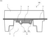
- Fig. 1 is a cross-sectional view showing an outline of a semiconductor hydrogen pressure sensor 100 according to embodiment 1, with protective film 12 omitted
- Fig. 2 is a cross-sectional view showing an outline of pressure-receiving chamber 7 of semiconductor hydrogen pressure sensor 100
- Fig. 3 is a diagram explaining the effect of semiconductor hydrogen pressure sensor 100
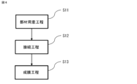
- Fig. 4 is a diagram showing the manufacturing process of semiconductor hydrogen pressure sensor 100 according to embodiment 1.
- Semiconductor hydrogen pressure sensor 100 is a sensor that directly receives pressure of a medium to be measured with semiconductor pressure detection element 3, without any other member such as oil between the part receiving the pressure of the medium to be measured and the detection element, measures the absolute pressure of the medium to be measured, and outputs the measurement result.
- the semiconductor hydrogen pressure sensor 100 includes a semiconductor pressure detection element 3 that receives the pressure of a measurement target medium containing hydrogen and electrically outputs a value corresponding to the absolute pressure of the measurement target medium, a bonding wire 10a extending from a terminal of the semiconductor pressure detection element 3, and a protective film 12 that continuously covers the semiconductor pressure detection element 3 and the bonding wire 10a that are exposed to the measurement target medium.
- the semiconductor hydrogen pressure sensor 100 includes a lead frame 11 that is insert-molded into a resin pressure-receiving chamber 7 to which the semiconductor pressure detection element 3 is fixed, and an ASIC 9 that is a signal processing circuit that is fixed to the inside of the pressure-receiving chamber 7 and connected to the semiconductor pressure detection element 3 via the bonding wire 10a and connected to the lead frame 11.
- the protective film 12 continuously covers the semiconductor pressure detection element 3, the bonding wire 10, the ASIC 9, and the pressure-receiving chamber 7 that are exposed to the measurement target medium.
- the bonding wire 10 is, for example, a wire made of gold.
- the semiconductor hydrogen pressure sensor 100 further comprises a pressure chamber 7 having an opening 7a for taking in the medium to be measured, with the semiconductor pressure detection element 3 and ASIC 9 fixed inside, and a pressure guiding tube 2 that communicates with the pressure chamber 7 via the opening 7a and takes in the medium to be measured from the outside into the pressure chamber 7.
- the medium to be measured is taken into the pressure chamber 7 from the outside through the pressure guiding tube 2 in the direction of the arrow shown in the figure.
- the medium to be measured is mainly hydrogen.
- the part of the housing 1 surrounding the pressure chamber 7, the pressure chamber 7, and the pressure guiding tube 2 are connected via an O-ring 8a.
- the pressure guiding tube 2 is connected to the external flow path (not shown) of the medium to be measured via an O-ring 8b. In this way, the part that serves as the flow path of the medium to be measured is sealed.
- the pressure-receiving chamber 7 is the portion that surrounds the semiconductor pressure detection element 3 and the ASIC 9, and is the portion in FIG. 2 where the protective film 12 is provided.
- the pressure-receiving chamber 7 is formed by insert molding in which resin is filled around the lead frame 11 used to send and receive electrical signals to and from the outside.
- the lead frame 11 is made of a metal such as copper.
- the lead frame 11 and the ASIC 9 are connected by bonding wires 10b.
- the portion that holds the pressure-receiving chamber 7 around the pressure-receiving chamber 7 is the housing 1 of the semiconductor hydrogen pressure sensor 100.
- the housing 1 is made of resin.
- the pressure-conducting tube 2 is also made of the same material as the housing 1.
- the housing 1 has a connector portion 5 that is used for connection to the outside.
- the connector portion 5 has a terminal 6 on the inside.
- the terminal 6 is made of a metal such as copper.
- the terminal 6 is electrically connected to the lead frame 11 by, for example, solder.
- the output of the semiconductor pressure detection element 3 is output to the outside from the terminal 6 via the ASIC 9.
- the semiconductor hydrogen pressure sensor 100 is small and lightweight because the housing 1 and pressure guiding tube 2 are made of resin, and the terminal 6 and lead frame 11 are integrated with resin.
- the semiconductor pressure detection element 3 receives the pressure of the medium to be measured, converts the pressure into an electrical signal, and outputs it.
- the ASIC 9 has the function of amplifying the electrical signal output by the semiconductor pressure detection element 3 and compensating the detected pressure characteristics for temperature and pressure.
- the semiconductor pressure detection element 3 is, for example, an element described in Patent No. 6300773.
- the semiconductor pressure detection element 3 receives hydrogen pressure directly with a single crystal silicon diaphragm and converts the distortion of the diaphragm into an electrical signal by a piezoresistor provided on its outer edge, etc., and has sufficiently high hydrogen reliability even when used in an environment directly exposed to pure hydrogen.
- the semiconductor pressure detection element 3 has a terminal on its surface that is connected to a bonding wire 10a. Although only one bonding wire 10a is shown in the figure, the number of bonding wires 10a and the number of terminals may be multiple.
- Fig. 11 is a cross-sectional view showing an outline of a semiconductor hydrogen pressure sensor 101 of the comparative example
- Fig. 12 is a cross-sectional view showing an outline of the pressure-receiving chamber 7 of the semiconductor hydrogen pressure sensor 101 of the comparative example
- Fig. 13 is a diagram showing a state in which a water droplet 13 is attached to the inside of the pressure-receiving chamber 7 of the semiconductor hydrogen pressure sensor 101 of the comparative example shown in Fig. 12.
- the semiconductor hydrogen pressure sensor 101 does not have a protective film 12, and the semiconductor pressure detection element 3, ASIC 9, and bonding wire 10 provided in the pressure-receiving chamber 7 are covered with gel 4.
- the semiconductor hydrogen pressure sensor 101 differs from the semiconductor hydrogen pressure sensor 100 in that the conductive parts of the semiconductor pressure detection element 3, ASIC 9, and bonding wire 10 are covered with gel 4.
- the gel 4 that covers the semiconductor pressure detection element 3 has a high protective effect under high temperature and normal pressure, even if the measurement medium is a corrosive liquid such as an acid.
- the measurement medium is absorbed into the gel 4 at a constant rate, albeit at a very slow rate over a period of several days.
- the water vapor contained in the measurement medium absorbed into the gel 4 may condense on the surface of the semiconductor pressure detection element 3, etc., which is relatively slightly cold.
- the areas where the water droplets 13 are attached include conductive parts.
- the conductive parts are the entire surface of the bonding wire 10, the outer edge of the bonding pad, which is the terminal on the semiconductor pressure detection element 3 that electrically connects the bonding wire 10a and the semiconductor pressure detection element 3, and the bonding part between the lead frame 11 and the bonding wire 10b. Even if condensation occurs, there is no problem if the system is stopped and power is not supplied to the semiconductor hydrogen pressure sensor 101. However, if the system operates without removing the condensation and power is supplied to the semiconductor hydrogen pressure sensor 101, a potential difference occurs between these conductive parts and any other conductive parts through the water droplets 13 that have condensed on the conductive parts. The resulting potential difference causes electrolysis to begin in the water droplets 13.
- This phenomenon causes corrosion of these conductive parts to begin. Although this phenomenon occurs under limited conditions and at a very slow speed, depending on the operating conditions of the system, this phenomenon is repeated and accumulated, so that there is a risk that the conductive parts where corrosion has occurred will break before the expected life of the system is reached.
- the protective film 12 which is a main part of the present application, will be described.
- the protective film 12 is continuously coated on the semiconductor pressure detection element 3 and the bonding wire 10 exposed to the medium to be measured.
- the parts to be coated with the protective film 12 are not limited to these, and in this embodiment, as shown in FIG. 2, the protective film 12 is coated on all parts where the pressure-receiving chamber 7 is formed.
- the protective film 12 is a polymer coating film having functions such as water repellency, water vapor impermeability, and acid corrosion resistance, and is preferably, for example, a parylene film that can be conformally coated.
- the protective film 12 is preferably formed, for example, by chemical vapor deposition (CVD).
- CVD chemical vapor deposition
- the protective film 12 formed by the above-mentioned manufacturing method using the above-mentioned material exhibits excellent coating properties because it penetrates not only the exposed surface of the adherend but also uniformly into the complex and intricate fine grooves and holes to protect the adherend.
- the film thickness can be precisely controlled, and the film thickness of the protective film 12 is preferably 2 to 10 ⁇ m.
- the thicker the protective film 12 the greater the residual stress of the protective film 12. Therefore, if the protective film 12 is thick, undesirable effects such as nonlinearity in the strain sensing characteristics of the piezoresistance will increase.
- the thickness of the protective film 12 is controlled within the above-mentioned range, thereby improving the protective effect of the protective film 12 and maintaining high-precision measurement in the semiconductor hydrogen pressure sensor 100.
- the semiconductor hydrogen pressure sensor 100 is configured such that only the protective film 12 is provided on the semiconductor pressure detection element 3 and bonding wire 10a etc. provided in the pressure-receiving chamber 7, the semiconductor hydrogen pressure sensor 100 is made smaller and lighter without increasing its size.
- the protective film 12 continuously covers the portions of the semiconductor pressure detection element 3, the bonding wire 10, the ASIC 9, and the pressure-receiving chamber 7 that are exposed to the medium to be measured, so that the inside of the pressure-receiving chamber 7 is effectively protected from condensation, and a semiconductor hydrogen pressure sensor 100 that is high accuracy and high reliability can be obtained.
- Fig. 14 is a schematic diagram showing an outline of the gas supply system of a typical PEFC type fuel cell system 1000, with related accessories omitted.
- the composition and state of the medium that is the object of measurement by the semiconductor hydrogen pressure sensor 100 will vary greatly depending on the configuration of the fuel cell system 1000 and the measurement position of the semiconductor hydrogen pressure sensor 100.
- the fuel cell system 1000 is composed of an anode subsystem and a cathode subsystem.
- the anode subsystem supplies hydrogen from a hydrogen fuel tank 20 to the fuel cell stack 19.
- the cathode subsystem supplies air from the outside to the fuel cell stack 19 and discharges water or water vapor generated by the reaction from the fuel cell stack 19 to the outside.
- the arrows in FIG. 14 indicate the direction of medium flow.
- pure hydrogen from the hydrogen fuel tank 20 is supplied to the fuel cell stack 19. Unreacted hydrogen and a portion of the water vapor generated by the reaction are merged with the pure hydrogen supplied from the hydrogen fuel tank 20 and supplied to the fuel cell stack 19 again in order to be recirculated to the fuel cell stack 19.
- the cathode subsystem the water and water vapor, which are by-products generated by the reaction, are discharged to the outside without being recirculated.
- the measurement medium of the semiconductor hydrogen pressure sensor 100 is the hydrogen gas supplied from the hydrogen fuel tank 20.
- the measurement medium in the A1 section is hydrogen gas with a purity of nearly 100%, and does not contain other gas components such as water vapor. Therefore, the semiconductor hydrogen pressure sensor 100, which has been designed and manufactured to have sufficient hydrogen reliability, does not have problematic water droplets adhering to it.
- the medium to be measured by the semiconductor hydrogen pressure sensor 100 is hydrogen, which is mainly composed of hydrogen but contains a certain amount of water vapor.
- Part A2 or part A3 is the location where the semiconductor hydrogen pressure sensor 100 is placed in the path where the above-mentioned recirculation takes place. Therefore, under certain composite conditions, the water vapor contained in the medium to be measured will condense on the surfaces of these components due to the temperature difference between the medium temperature and the semiconductor pressure detection element 3, ASIC 9, bonding wire 10, etc. Also, depending on the operating state of the system, a medium containing water droplets may flow in the path where recirculation takes place.
- the relatively hot and humid medium returning from the recirculation path meets the relatively cold and dry hydrogen supplied from the hydrogen fuel tank 20, so the medium flowing in from the recirculation path side is rapidly cooled, making it easy for condensation to form on the semiconductor hydrogen pressure sensor 100, and problematic water droplets may adhere to the semiconductor hydrogen pressure sensor 100.
- the medium to be measured by the semiconductor hydrogen pressure sensor 100 is basically air taken in from the outside.
- hydrogen gas may diffuse from the anode side through the fuel cell stack 19, and a certain level of hydrogen resistance is required to measure the pressure, so the semiconductor hydrogen pressure sensor 100 is also used in the C1 section.
- the semiconductor hydrogen pressure sensor 100 is used, problematic water droplets do not adhere to the semiconductor hydrogen pressure sensor 100.
- the medium to be measured by the semiconductor hydrogen pressure sensor 100 is a gas containing water or water vapor that is generated as a by-product of the reaction and discharged from the fuel cell stack 19.
- the C2 section is the location where the problematic water droplets are most likely to adhere to the semiconductor hydrogen pressure sensor 100.
- the C2 section is the location where water, a by-product of the reaction, is generated, in accordance with the principles of the fuel cell. If no special measures such as purging are taken, the medium is almost always at a high humidity of 90% or more while the system is operating, and part of the medium is in the form of water droplets. Therefore, it is necessary to assume a situation in which water droplets 13 are always attached to the surfaces of the semiconductor pressure detection element 3, ASIC 9, and bonding wire 10, as shown in Figure 3.
- a protective film 12 is provided on the surfaces of the semiconductor pressure detection element 3, the ASIC 9, and the bonding wire 10. Therefore, even if condensation occurs on the semiconductor hydrogen pressure sensor 100 and water droplets are present, the water droplets are physically and electrically insulated from these conductive parts, so that electrolysis does not occur in the water droplets and corrosion does not occur, which is a significant effect of improving reliability. Even if the fuel cell system 1000 is in an operating state and power is supplied to the semiconductor hydrogen pressure sensor 100, the effect of improving reliability can be obtained in a similar manner.
- the method for manufacturing the semiconductor hydrogen pressure sensor 100 will be described with reference to Fig. 4.
- the method for manufacturing the semiconductor hydrogen pressure sensor 100 includes a member preparation step (S11), a connection step (S12), and a film formation step (S13).
- the component preparation process is a process of preparing the semiconductor pressure detection element 3, which receives the pressure of the medium to be measured and electrically outputs a value corresponding to the absolute pressure of the medium to be measured, and the bonding wire 10.
- the semiconductor hydrogen pressure sensor 100 shown in FIG. 1 further includes an ASIC 9, a lead frame 11, a pressure-receiving chamber 7, a terminal 6, O-rings 8a, 8b, and a pressure guiding tube 2, and these are also prepared in this process.
- the connection process is a process of electrically connecting the bonding wire 10a to the semiconductor pressure detection element 3.
- the pressure-receiving chamber 7 that takes in the medium to be measured is formed around the lead frame 11 by insert molding.
- the portion of the lead frame 11 that is connected to the bonding wire 10b is exposed to the outside.
- the semiconductor pressure detection element 3 and the ASIC 9 are fixed inside the pressure-receiving chamber 7, the semiconductor pressure detection element 3 and the ASIC 9 are connected by the bonding wire 10a, and the ASIC 9 is connected to the portion of the lead frame 11 exposed to the outside by the bonding wire 10b.
- the semiconductor pressure detection element 3 and the ASIC 9 are arranged side by side and fixed to the surface of the lead frame 11 on the side of the pressure-receiving chamber 7 via resin.
- the fixing method is, for example, adhesion.
- the film forming process is a process in which the portions of the semiconductor pressure detection element 3 and the bonding wire 10a that are exposed to the medium to be measured are continuously covered with a protective film 12.
- the protective film 12 continuously covers the portions of the semiconductor pressure detection element 3, the bonding wire 10, the ASIC 9, and the pressure-receiving chamber 7 that are exposed to the medium to be measured.
- the protective film 12 is, for example, a polymer coating film, and is formed by chemical vapor deposition.
- the terminals 6 are electrically connected to the lead frame 11, for example by soldering.
- the housing 1 is formed around the pressure-receiving chamber 7 by insert molding.
- the part of the housing 1 around the pressure-receiving chamber 7, the pressure-receiving chamber 7, and the pressure guiding tube 2 are connected via an O-ring 8a.
- the flow path (not shown) of the external medium to be measured is connected to the pressure guiding tube 2 via an O-ring 8b.
- the semiconductor hydrogen pressure sensor 100 includes a semiconductor pressure detection element 3 that receives the pressure of a measurement medium containing hydrogen and electrically outputs a value corresponding to the absolute pressure of the measurement medium, a bonding wire 10a extending from the terminal of the semiconductor pressure detection element 3, and a protective film 12 that continuously covers the semiconductor pressure detection element 3 and the bonding wire 10a that are exposed to the measurement medium. Therefore, even if condensation occurs on the protective film 12, water droplets 13 do not adhere to the conductive parts of the semiconductor pressure detection element 3 and the bonding wire 10a, and corrosion and breakage of the conductive parts due to electrolysis of the water droplets 13 do not occur. Therefore, a semiconductor hydrogen pressure sensor 100 that is small, lightweight, and highly accurate and reliable can be obtained.
- the protective film 12 continuously covers the semiconductor pressure detection element 3, the bonding wire 10, the ASIC 9, and the pressure chamber 7 exposed to the medium to be measured, the inside of the pressure chamber 7 is effectively protected from condensation, and a semiconductor hydrogen pressure sensor 100 with high accuracy and high reliability can be obtained.
- the protective film 12 is a polymer coating film
- the polymer coating film has functions such as water repellency, water vapor impermeability, and acid corrosion resistance, so that even if condensation occurs on the protective film 12, adhesion of water droplets 13 to the conductive parts of the semiconductor pressure detection element 3 and the bonding wire 10a is reliably suppressed, and corrosion and disconnection of the conductive parts due to electrolysis of the water droplets 13 do not occur, and a semiconductor hydrogen pressure sensor 100 with high accuracy and high reliability can be obtained.
- the manufacturing method of the semiconductor hydrogen pressure sensor 100 includes a component preparation step of preparing the semiconductor pressure detection element 3, which receives the pressure of the medium to be measured and electrically outputs a value corresponding to the absolute pressure of the medium to be measured, and the bonding wire 10a, a connection step of electrically connecting the bonding wire 10a to the semiconductor pressure detection element 3, and a film formation step of continuously covering the parts of the semiconductor pressure detection element 3 and the bonding wire 10a exposed to the medium to be measured with a protective film 12. Therefore, even if condensation occurs on the protective film 12, water droplets 13 do not adhere to the conductive parts of the semiconductor pressure detection element 3 and the bonding wire 10a, and corrosion and breakage of the conductive parts due to electrolysis of the water droplets 13 do not occur. Therefore, it is possible to manufacture a semiconductor hydrogen pressure sensor 100 that is small, lightweight, and has high accuracy and high reliability.
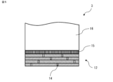
- Fig. 5 is a cross-sectional view showing a main portion of the pressure-receiving chamber 7 of the semiconductor hydrogen pressure sensor 100 according to the second embodiment, and is an enlarged view of the portion of the semiconductor pressure detection element 3 on the side of the medium to be measured, showing the semiconductor base 16, terminals 15, and protective film 12.
- the semiconductor hydrogen pressure sensor 100 according to the second embodiment has a laminated protective film 12.
- the protective film 12 is a laminated film in which multiple films are laminated. The reason for laminating the protective film 12 will be explained.
- the bonding pad portion where the semiconductor pressure detection element 3 and the bonding wire 10a are electrically connected there may be a portion where the terminal 15, which is a conductive portion, is exposed.
- such a portion is also basically covered with the protective film 12 formed conformally.
- a minute defect 14 such as a pinhole may be generated in the protective film 12, and it is very difficult to completely prevent the occurrence of the defect 14. If such a defect 14 occurs in a conductive portion such as the terminal 15 and connects the terminal 15 to the outside, a circuit through the infiltrated water droplets is formed at the defect 14 portion when power is supplied, and electrolysis may occur in the water droplets.
- the protective film 12 When the protective film 12 is formed as a laminated film in which multiple films are stacked, the protective film 12 can be stacked so that the defects 14 do not connect to each other, as shown in FIG. 5. Because the defects 14 do not connect to each other, it is possible to prevent the terminal 15 from communicating with the outside via the defects 14.
- the protective film 12 to be stacked may be the same as that in embodiment 1. If a thick film is formed continuously at one time, there is a high risk that the defects 14 will communicate with each other. Therefore, by forming a laminated structure by stopping the film formation once during film formation and then restarting the film formation, etc., it is possible to form a protective film 12 structure in which the defects 14 do not communicate with the outside.
- Defects 14 will occur with a certain probability during film formation, but unless the defects 14 occur in the same position each time the film is laminated, overlap, and connect, the defects 14 will not penetrate the entire protective film 12.
- the probability of defects 14 penetrating the protective film 12 is proportional to the product of the probabilities of defects 14 occurring in each laminated film, so the more layers there are, the more significantly the probability of defects 14 penetrating the protective film 12 can be reduced.
- the number of layers of the protective film 12 should be appropriately selected from a few layers to around 10 layers, taking into account the overall thickness and residual stress of the protective film 12.
- the protective film 12 is a laminated film in which multiple films are stacked, so even if there is a tiny defect 14 such as a pinhole in the protective film 12 provided on the semiconductor pressure detection element 3, the defect 14 can be prevented from communicating with the outside. Because the defect 14 does not communicate with the outside, water droplets can be prevented from reaching the surface of the semiconductor pressure detection element 3 even if the medium to be measured is a high humidity medium containing a large amount of water vapor. Because water droplets do not reach the surface of the semiconductor pressure detection element 3, the reliability of the semiconductor hydrogen pressure sensor 100 can be improved.
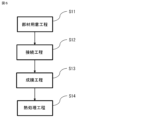
- FIG. 6 is a diagram showing the manufacturing process for the semiconductor hydrogen pressure sensor 100 according to embodiment 3
- Fig. 7 is a diagram showing the variation in residual stress when the protective film 12 of the semiconductor hydrogen pressure sensor 100 is placed in a constant high temperature environment.
- a heat treatment process is added to the manufacturing method for the semiconductor hydrogen pressure sensor 100 according to embodiment 3.
- the protective film 12 of the semiconductor hydrogen pressure sensor 100 according to embodiment 3 is subjected to heat treatment.
- the method of manufacturing the semiconductor hydrogen pressure sensor 100 includes a heat treatment step (S14) in which heat treatment is performed on the protective film 12 portion after the film formation step (S13) shown in embodiment 1.
- the protective film 12 is, for example, a parylene film.
- parylene films have the characteristic that the residual stress varies with the applied time, as shown in FIG. 7, even at about 100°C, which is roughly the maximum temperature of the medium used in PEFC-type fuel cell systems. In other words, the residual stress increases with time up to a certain time, but once that time is exceeded, the amount of variation in the residual stress saturates and stabilizes.
- the semiconductor hydrogen pressure sensor 100 will deviate from its intended detection characteristics, and the measurement accuracy of the semiconductor hydrogen pressure sensor 100 will decrease.
- the detection characteristics of the semiconductor hydrogen pressure sensor 100 will fluctuate while the semiconductor hydrogen pressure sensor 100 is in use. In either case, the high-precision measurement of the semiconductor hydrogen pressure sensor 100 will be hindered.
- heat treatment is performed for a time until the residual stress in FIG. 7 reaches the region where it stabilizes, thereby preventing the semiconductor hydrogen pressure sensor 100 from impeding high-precision measurement.
- the applied temperature can be set slightly higher than the temperature range used in the actual system to shorten the heat treatment time.
- the manufacturing method of the semiconductor hydrogen pressure sensor 100 according to embodiment 3 includes a heat treatment process in which heat treatment is performed on the protective film 12 portion after the film formation process, so that the residual stress of the protective film 12 is stabilized to a state that is not fluctuated by external factors such as high temperature, and the detection characteristics of the semiconductor hydrogen pressure sensor 100 do not fluctuate, and the high measurement accuracy of the semiconductor hydrogen pressure sensor 100 can be maintained over the expected warranty period.
- the protective film 12 of the semiconductor hydrogen pressure sensor 100 according to embodiment 3 has been heat treated, the detection characteristics of the semiconductor hydrogen pressure sensor 100 do not fluctuate, and the high measurement accuracy of the semiconductor hydrogen pressure sensor 100 can be maintained over the expected warranty period.
- FIG. 8 is a cross-sectional view showing an outline of the pressure-receiving chamber 7 of the semiconductor hydrogen pressure sensor 100 according to embodiment 4.
- the semiconductor hydrogen pressure sensor 100 according to embodiment 4 has a configuration in which a gel-like member is added.
- the surface of the protective film 12 covering the semiconductor pressure detection element 3 is covered with a gel-like material.
- gel 4a is provided on the surface of the protective film 12 covering the semiconductor pressure detection element 3
- gel 4b is provided on the surface of the protective film 12 covering the ASIC 9.
- the gel-like material is, for example, silicone gel. The reason for adding the gel-like material is explained below.
- the protective film 12 is provided on the surface of the conductive portion inside the pressure chamber 7, water droplets due to condensation form on the protective film 12, and even if power is supplied to the semiconductor hydrogen pressure sensor 100 during system operation, electrolysis does not occur in the water droplets.
- the configuration shown in FIG. 2 does not use gel 4, the shock mitigation effect of gel 4 cannot be obtained.
- the gel 4 also has the function of preventing physical damage to the pressure-receiving diaphragm on the surface of the semiconductor pressure detection element 3 due to the impact of a solid foreign object or the like colliding with the semiconductor pressure detection element 3 at high speed.
- the surface of the protective film 12 covering the semiconductor pressure detection element 3 is covered with a gel-like material, so that the pressure-receiving diaphragm of the semiconductor pressure detection element 3 can be prevented from being damaged by impacts caused by collisions with particulate foreign matter that have entered from the outside.
- FIG. 9 is a cross-sectional view showing an outline of the semiconductor hydrogen pressure sensor 100 according to the fifth embodiment, in which the protective film 12 is omitted.
- the semiconductor hydrogen pressure sensor 100 according to the fifth embodiment is configured such that the pressure guiding tube 2 has a moisture absorbing member 17.
- the pressure guiding tube 2 has a moisture absorbing member 17 at the end of the pressure guiding tube 2 that takes in the medium to be measured.
- the moisture absorbing member 17 is provided, for example, on the entire circumference of the inner wall surface at the tip of the pressure guiding tube 2 in a state of contact with the medium to be measured.
- the moisture absorbing member 17 is, for example, silica gel that adsorbs water.
- the semiconductor hydrogen pressure sensor 100 has a moisture absorbing member 17 at the end of the pressure guiding tube 2 where the medium to be measured is taken in. Therefore, even if the medium to be measured contains a large amount of water droplets and water vapor, these are absorbed by the moisture absorbing member 17, and the amount of water droplets and water vapor that reaches the pressure-receiving chamber 7 can be significantly reduced. Because the amount of water droplets and water vapor that reaches the pressure-receiving chamber 7 is significantly reduced, the risk of condensation in a specific complex environment and corrosion of conductive parts due to electrolysis caused by condensation can be significantly reduced.
- FIG. 10 is a cross-sectional view showing an outline of the semiconductor hydrogen pressure sensor 100 according to embodiment 6, with the protective film 12 omitted.
- the semiconductor hydrogen pressure sensor 100 according to embodiment 6 has a configuration in which the pressure guiding tube 2 has a heating section 18.
- the pressure guiding tube 2 has a heating section 18 adjacent to the moisture absorbing member 17.
- the heating section 18 is disposed, for example, surrounding the moisture absorbing member 17.
- the heating section 18 is, for example, a heater that is heated electrically. The reason for adding the heating section 18 is explained below.
- the moisture absorbing member 17 at the end of the pressure guiding tube 2, the amount of water vapor that reaches the pressure receiving chamber 7 can be reduced, improving the reliability of the semiconductor hydrogen pressure sensor 100.
- the water vapor absorbed by the moisture absorbing member 17 can be released by driving the heating section 18 as part of a series of sequence operations when the fuel cell system 1000 is stopped, etc.
- the released water vapor is discharged to the outside so that it does not remain in the pressure receiving chamber 7, and the inside of the pressure guiding tube 2 and the inside of the pressure receiving chamber 7 can be made into a dry environment.
- the moisture absorbing function of the moisture absorbing member 17 can be restored. This makes it possible to obtain a semiconductor hydrogen pressure sensor 100 that has stable reliability over a long period of time.
- the pressure guiding tube 2 has the heating section 18 adjacent to the moisture absorbent member 17, so that the moisture absorbed by the moisture absorbent member 17 can be vaporized, and the reduced moisture absorption capacity of the moisture absorbent member 17 can be restored. Because the moisture absorption capacity of the moisture absorbent member 17 is restored, the semiconductor hydrogen pressure sensor 100 can maintain high reliability for a long period of time, even if the medium being measured has a high humidity.
Landscapes
- Physics & Mathematics (AREA)
- General Physics & Mathematics (AREA)
- Chemical & Material Sciences (AREA)
- Analytical Chemistry (AREA)
- Measuring Fluid Pressure (AREA)
Abstract
Description
図1は実施の形態1に係る半導体水素圧力センサ100の概略を示す断面図で、保護膜12を省略して示した図、図2は半導体水素圧力センサ100の受圧室7の概略を示す断面図、図3は半導体水素圧力センサ100の効果を説明する図、図4は実施の形態1に係る半導体水素圧力センサ100の製造工程を示す図である。半導体水素圧力センサ100は、測定対象媒体の圧力を受ける部分と検出素子との間にオイルなどの他の部材を介すことなく、半導体圧力検出素子3で測定対象媒体を直接受圧して、測定対象媒体の絶対圧を測定し、測定結果を出力するセンサである。
半導体水素圧力センサ100は、図2に示すように、水素を含有した測定対象媒体の圧力を受圧し、測定対象媒体の絶対圧に応じた値を電気的に出力する半導体圧力検出素子3と、半導体圧力検出素子3の端子から延びたボンディングワイヤ10aと、測定対象媒体に露出した、半導体圧力検出素子3及びボンディングワイヤ10aの部分を、連続して被覆した保護膜12とを備える。本実施の形態では、半導体水素圧力センサ100は、内側に半導体圧力検出素子3が固定された樹脂製の受圧室7にインサート成形されたリードフレーム11と、受圧室7の内側に固定され、半導体圧力検出素子3にボンディングワイヤ10aを介して接続され、リードフレーム11に接続された信号処理回路であるASIC9とを備える。また本実施の形態では、保護膜12は、測定対象媒体に露出した、半導体圧力検出素子3、ボンディングワイヤ10、ASIC9、及び受圧室7の部分を、連続して被覆している。ボンディングワイヤ10は、例えば、金からなるワイヤである。
本願の要部である保護膜12の説明に先立ち、比較例について説明する。図11は比較例の半導体水素圧力センサ101の概略を示す断面図、図12は比較例の半導体水素圧力センサ101の受圧室7の概略を示す断面図、図13は図12に示した比較例の半導体水素圧力センサ101の受圧室7の内側に水滴13が付いた様子を示す図である。半導体水素圧力センサ101は、保護膜12を有さず、受圧室7に設けられた半導体圧力検出素子3、ASIC9、及びボンディングワイヤ10がゲル4により覆われている。半導体水素圧力センサ101は、半導体圧力検出素子3、ASIC9、及びボンディングワイヤ10が有した導電部がゲル4により覆われている点で、半導体水素圧力センサ100と異なっている。
本願の要部である保護膜12について説明する。導電部に水滴13を付着させないために、保護膜12は、測定対象媒体に露出した、半導体圧力検出素子3及びボンディングワイヤ10の部分に、連続して被覆されている。保護膜12で被覆する部分はこれに限るものではなく、本実施の形態では、図2に示すように、受圧室7が形成される全ての箇所に保護膜12が被覆されている。保護膜12は、撥水性、水蒸気不透過性、酸腐食耐性等の機能を有するポリマー・コーティング・フィルムであって、例えば、コンフォーマルにコーティングできるパリレン膜が好適である。保護膜12は、例えば、化学蒸着法(CVD)により形成することが好ましい。化学蒸着法により保護膜12を形成することで、被覆の効果を最大化するために、導電部の表面のみならず、受圧室7の内壁にも連続的にコーティングすることができる。
本実施の形態に示した半導体水素圧力センサ100の燃料電池システム1000への適用箇所と水滴の関係について、図14を用いて説明する。図14は、典型的なPEFC型の燃料電池システム1000のガス供給系の概略を示す模式図で、関連補器類は省略している。半導体水素圧力センサ100が測定対象とする媒体の組成及び状態は、燃料電池システム1000の構成、及び半導体水素圧力センサ100の測定位置によって大きく異なる。
半導体水素圧力センサ100の製造方法について、図4を用いて説明する。半導体水素圧力センサ100の製造方法は、部材用意工程(S11)、接続工程(S12)、及び成膜工程(S13)を備える。
実施の形態2に係る半導体水素圧力センサ100について説明する。図5は実施の形態2に係る半導体水素圧力センサ100の受圧室7の要部を示す断面図で、半導体圧力検出素子3の測定対象媒体の側の部分を拡大して、半導体基部16、端子15、及び保護膜12の部分を示した図である。実施の形態2に係る半導体水素圧力センサ100は、保護膜12が積層された構成になっている。
実施の形態3に係る半導体水素圧力センサ100の製造方法について説明する。図6は実施の形態3に係る半導体水素圧力センサ100の製造工程を示す図、図7は半導体水素圧力センサ100の保護膜12を一定の高温環境下においた場合の残留応力の変動を示した図である。実施の形態3に係る半導体水素圧力センサ100の製造方法は、熱処理工程が追加されている。実施の形態3に係る半導体水素圧力センサ100の保護膜12は、熱処理が行われている。
実施の形態4に係る半導体水素圧力センサ100について説明する。図8は実施の形態4に係る半導体水素圧力センサ100の受圧室7の概略を示す断面図である。実施の形態4に係る半導体水素圧力センサ100は、ゲル状の部材が追加された構成になっている。
実施の形態5に係る半導体水素圧力センサ100について説明する。図9は実施の形態5に係る半導体水素圧力センサ100の概略を示す断面図で、保護膜12を省略して示した図である。実施の形態5に係る半導体水素圧力センサ100は、導圧管2が吸湿部材17を有した構成になっている。
実施の形態6に係る半導体水素圧力センサ100について説明する。図10は実施の形態6に係る半導体水素圧力センサ100の概略を示す断面図で、保護膜12を省略して示した図である。実施の形態6に係る半導体水素圧力センサ100は、導圧管2が加熱部18を有した構成になっている。
従って、例示されていない無数の変形例が、本願明細書に開示される技術の範囲内において想定される。例えば、少なくとも1つの構成要素を変形する場合、追加する場合または省略する場合、さらには、少なくとも1つの構成要素を抽出し、他の実施の形態の構成要素と組み合わせる場合が含まれるものとする。
Claims (10)
- 水素を含有した測定対象媒体の圧力を受圧し、前記測定対象媒体の絶対圧に応じた値を電気的に出力する半導体圧力検出素子と、
前記半導体圧力検出素子の端子から延びたボンディングワイヤと、
前記測定対象媒体に露出した、前記半導体圧力検出素子及び前記ボンディングワイヤの部分を、連続して被覆した保護膜と、を備えた半導体水素圧力センサ。 - 前記保護膜は、複数の膜が積層された積層膜である請求項1に記載の半導体水素圧力センサ。
- 前記半導体圧力検出素子を被覆した前記保護膜の表面が、ゲル状の部材で覆われている請求項1又は2に記載の半導体水素圧力センサ。
- 前記半導体圧力検出素子が内側に固定され、前記測定対象媒体を内側に取り込む開口部を有した受圧室と、
前記開口部を介して前記受圧室と連通し、前記測定対象媒体を外部から前記受圧室に取り込む導圧管と、を備え、
前記導圧管は、前記測定対象媒体を取り込む前記導圧管の端部に吸湿部材を有している請求項1から3のいずれか1項に記載の半導体水素圧力センサ。 - 前記導圧管は、前記吸湿部材に隣接した加熱部を有している請求項4に記載の半導体水素圧力センサ。
- 内側に前記半導体圧力検出素子が固定された樹脂製の受圧室と、
前記受圧室にインサート成形されたリードフレームと、
前記受圧室の内側に固定され、前記半導体圧力検出素子に前記ボンディングワイヤを介して接続され、前記リードフレームに接続された信号処理回路と、を更に備え、
前記保護膜は、前記測定対象媒体に露出した、前記半導体圧力検出素子、前記ボンディングワイヤ、前記信号処理回路、及び前記受圧室の部分を、連続して被覆している請求項1から3のいずれか1項に記載の半導体水素圧力センサ。 - 前記保護膜は、ポリマー・コーティング・フィルムである請求項1から6のいずれか1項に記載の半導体水素圧力センサ。
- 前記保護膜は、熱処理が行われている請求項7に記載の半導体水素圧力センサ。
- 測定対象媒体の圧力を受圧し、前記測定対象媒体の絶対圧に応じた値を電気的に出力する半導体圧力検出素子、及びボンディングワイヤを用意する部材用意工程と、
前記ボンディングワイヤを前記半導体圧力検出素子に電気的に接続する接続工程と、
前記測定対象媒体に露出した、前記半導体圧力検出素子及び前記ボンディングワイヤの部分を、保護膜により連続して被覆する成膜工程と、を備えた半導体水素圧力センサの製造方法。 - 前記成膜工程の後に、前記保護膜の部分に熱処理を行う熱処理工程を備えた請求項9に記載の半導体水素圧力センサの製造方法。
Priority Applications (5)
| Application Number | Priority Date | Filing Date | Title |
|---|---|---|---|
| DE112023005828.8T DE112023005828T5 (de) | 2023-02-21 | 2023-02-21 | Halbleiter-Wasserstoffdrucksensor und Verfahren zur Herstellung desselben |
| US19/113,094 US20260092824A1 (en) | 2023-02-21 | 2023-02-21 | Semiconductor hydrogen pressure sensor and method for manufacturing same |
| KR1020257013721A KR20250073439A (ko) | 2023-02-21 | 2023-02-21 | 반도체 수소 압력 센서 및 그 제조 방법 |
| PCT/JP2023/006252 WO2024176356A1 (ja) | 2023-02-21 | 2023-02-21 | 半導体水素圧力センサ及びその製造方法 |
| JP2025501982A JPWO2024176356A1 (ja) | 2023-02-21 | 2023-02-21 |
Applications Claiming Priority (1)
| Application Number | Priority Date | Filing Date | Title |
|---|---|---|---|
| PCT/JP2023/006252 WO2024176356A1 (ja) | 2023-02-21 | 2023-02-21 | 半導体水素圧力センサ及びその製造方法 |
Publications (1)
| Publication Number | Publication Date |
|---|---|
| WO2024176356A1 true WO2024176356A1 (ja) | 2024-08-29 |
Family
ID=92500419
Family Applications (1)
| Application Number | Title | Priority Date | Filing Date |
|---|---|---|---|
| PCT/JP2023/006252 Ceased WO2024176356A1 (ja) | 2023-02-21 | 2023-02-21 | 半導体水素圧力センサ及びその製造方法 |
Country Status (5)
| Country | Link |
|---|---|
| US (1) | US20260092824A1 (ja) |
| JP (1) | JPWO2024176356A1 (ja) |
| KR (1) | KR20250073439A (ja) |
| DE (1) | DE112023005828T5 (ja) |
| WO (1) | WO2024176356A1 (ja) |
Citations (7)
| Publication number | Priority date | Publication date | Assignee | Title |
|---|---|---|---|---|
| JPH05223670A (ja) * | 1992-02-17 | 1993-08-31 | Fujikura Ltd | 半導体圧力センサ |
| JP2001318014A (ja) * | 2000-03-25 | 2001-11-16 | Robert Bosch Gmbh | 薄膜構成素子の製造方法 |
| JP2002206979A (ja) * | 2001-01-09 | 2002-07-26 | Yamatake Corp | 圧力センサ用吸湿部材 |
| JP2007040772A (ja) * | 2005-08-02 | 2007-02-15 | Mitsubishi Electric Corp | 半導体圧力センサ |
| JP2007292547A (ja) * | 2006-04-24 | 2007-11-08 | Mitsubishi Electric Corp | 圧力センサ、圧力センサの検査方法 |
| US20180148320A1 (en) * | 2016-11-29 | 2018-05-31 | Taiwan Semiconductor Manufacturing Co., Ltd. | Multi-layer sealing film for high seal yield |
| JP6425794B1 (ja) * | 2017-12-13 | 2018-11-21 | 三菱電機株式会社 | 半導体圧力センサ |
Family Cites Families (2)
| Publication number | Priority date | Publication date | Assignee | Title |
|---|---|---|---|---|
| JP2007144783A (ja) * | 2005-11-28 | 2007-06-14 | Nakato Kenkyusho:Kk | 水素バリヤー性被覆物、成形体及び水素バリヤー性被覆物の製造方法 |
| JP4985572B2 (ja) * | 2008-07-10 | 2012-07-25 | 株式会社デンソー | 圧力センサ |
-
2023
- 2023-02-21 DE DE112023005828.8T patent/DE112023005828T5/de active Pending
- 2023-02-21 JP JP2025501982A patent/JPWO2024176356A1/ja active Pending
- 2023-02-21 KR KR1020257013721A patent/KR20250073439A/ko active Pending
- 2023-02-21 US US19/113,094 patent/US20260092824A1/en active Pending
- 2023-02-21 WO PCT/JP2023/006252 patent/WO2024176356A1/ja not_active Ceased
Patent Citations (7)
| Publication number | Priority date | Publication date | Assignee | Title |
|---|---|---|---|---|
| JPH05223670A (ja) * | 1992-02-17 | 1993-08-31 | Fujikura Ltd | 半導体圧力センサ |
| JP2001318014A (ja) * | 2000-03-25 | 2001-11-16 | Robert Bosch Gmbh | 薄膜構成素子の製造方法 |
| JP2002206979A (ja) * | 2001-01-09 | 2002-07-26 | Yamatake Corp | 圧力センサ用吸湿部材 |
| JP2007040772A (ja) * | 2005-08-02 | 2007-02-15 | Mitsubishi Electric Corp | 半導体圧力センサ |
| JP2007292547A (ja) * | 2006-04-24 | 2007-11-08 | Mitsubishi Electric Corp | 圧力センサ、圧力センサの検査方法 |
| US20180148320A1 (en) * | 2016-11-29 | 2018-05-31 | Taiwan Semiconductor Manufacturing Co., Ltd. | Multi-layer sealing film for high seal yield |
| JP6425794B1 (ja) * | 2017-12-13 | 2018-11-21 | 三菱電機株式会社 | 半導体圧力センサ |
Also Published As
| Publication number | Publication date |
|---|---|
| JPWO2024176356A1 (ja) | 2024-08-29 |
| US20260092824A1 (en) | 2026-04-02 |
| DE112023005828T5 (de) | 2025-12-18 |
| KR20250073439A (ko) | 2025-05-27 |
Similar Documents
| Publication | Publication Date | Title |
|---|---|---|
| JP5884921B2 (ja) | 圧力センサ装置および圧力センサ装置の製造方法 | |
| EP0736757B1 (en) | Media compatible pressure transducer by inorganic protection coating of the cavity | |
| EP1947439B1 (en) | Semiconductor pressure sensor | |
| US7373819B2 (en) | Stress sensitive humidity sensor based on a MEMS structure | |
| JP6300773B2 (ja) | 半導体圧力センサ | |
| US20260098845A1 (en) | Gas sensor with a sensor element and a flame arrester and use of the same for the detection of gases | |
| CN101548165B (zh) | 压力传感器 | |
| US8826725B2 (en) | Gas detector | |
| US20260092824A1 (en) | Semiconductor hydrogen pressure sensor and method for manufacturing same | |
| KR20050002850A (ko) | 반도체형 센서 및 반도체 장치의 도금 방법 | |
| US8689609B2 (en) | Hydrogen sensor with dew condensation prevention | |
| JP2005326338A (ja) | 圧力センサ | |
| JP7630731B1 (ja) | 半導体センサ及びその製造方法 | |
| JP4893529B2 (ja) | 圧力センサ | |
| US8839660B2 (en) | Liquid water protected implementation of a gas quality hydrogen sensor into a fuel cell exhaust system | |
| WO2009054658A1 (en) | Apparatus for measuring concentration of liquid fuel using strain gauge and fuel cell including apparatus | |
| JP6621434B2 (ja) | Memsセンサ | |
| Yoshikawa et al. | A Highly Durable MEMS Hydrogen Pressure Sensor for Fuel Cell Systems Using Atomic Layer Deposited Al 2 O 3/Parylene-C Hybrid Barrier Coating | |
| US12422323B2 (en) | Protection structure for pressure sensor device | |
| JP4882682B2 (ja) | 圧力センサ装置 | |
| GB2627989A (en) | Passivation of metal structures for harsh environments | |
| CN121898678A (zh) | 压阻式压力传感器以及制造这种压阻式压力传感器的方法 | |
| CN119895625A (zh) | 用于检测湿气侵入的装置 |
Legal Events
| Date | Code | Title | Description |
|---|---|---|---|
| 121 | Ep: the epo has been informed by wipo that ep was designated in this application |
Ref document number: 23924010 Country of ref document: EP Kind code of ref document: A1 |
|
| WWE | Wipo information: entry into national phase |
Ref document number: 2025501982 Country of ref document: JP |
|
| ENP | Entry into the national phase |
Ref document number: 20257013721 Country of ref document: KR Kind code of ref document: A |
|
| WWE | Wipo information: entry into national phase |
Ref document number: 1020257013721 Country of ref document: KR |
|
| WWE | Wipo information: entry into national phase |
Ref document number: 112023005828 Country of ref document: DE |
|
| WWP | Wipo information: published in national office |
Ref document number: 112023005828 Country of ref document: DE |
|
| 122 | Ep: pct application non-entry in european phase |
Ref document number: 23924010 Country of ref document: EP Kind code of ref document: A1 |