WO2024171710A1 - アンテナ部品 - Google Patents
アンテナ部品 Download PDFInfo
- Publication number
- WO2024171710A1 WO2024171710A1 PCT/JP2024/001284 JP2024001284W WO2024171710A1 WO 2024171710 A1 WO2024171710 A1 WO 2024171710A1 JP 2024001284 W JP2024001284 W JP 2024001284W WO 2024171710 A1 WO2024171710 A1 WO 2024171710A1
- Authority
- WO
- WIPO (PCT)
- Prior art keywords
- conductor layer
- axis
- radiating
- antenna component
- region
- Prior art date
- Legal status (The legal status is an assumption and is not a legal conclusion. Google has not performed a legal analysis and makes no representation as to the accuracy of the status listed.)
- Ceased
Links
Images






Classifications
-
- H—ELECTRICITY
- H01—ELECTRIC ELEMENTS
- H01Q—ANTENNAS, i.e. RADIO AERIALS
- H01Q1/00—Details of, or arrangements associated with, antennas
- H01Q1/36—Structural form of radiating elements, e.g. cone, spiral, umbrella; Particular materials used therewith
- H01Q1/38—Structural form of radiating elements, e.g. cone, spiral, umbrella; Particular materials used therewith formed by a conductive layer on an insulating support
-
- H—ELECTRICITY
- H01—ELECTRIC ELEMENTS
- H01Q—ANTENNAS, i.e. RADIO AERIALS
- H01Q1/00—Details of, or arrangements associated with, antennas
- H01Q1/12—Supports; Mounting means
- H01Q1/22—Supports; Mounting means by structural association with other equipment or articles
- H01Q1/2283—Supports; Mounting means by structural association with other equipment or articles mounted in or on the surface of a semiconductor substrate as a chip-type antenna or integrated with other components into an IC package
-
- H—ELECTRICITY
- H01—ELECTRIC ELEMENTS
- H01Q—ANTENNAS, i.e. RADIO AERIALS
- H01Q13/00—Waveguide horns or mouths; Slot antennas; Leaky-waveguide antennas; Equivalent structures causing radiation along the transmission path of a guided wave
- H01Q13/08—Radiating ends of two-conductor microwave transmission lines, e.g. of coaxial lines, of microstrip lines
-
- H—ELECTRICITY
- H01—ELECTRIC ELEMENTS
- H01Q—ANTENNAS, i.e. RADIO AERIALS
- H01Q9/00—Electrically-short antennas having dimensions not more than twice the operating wavelength and consisting of conductive active radiating elements
- H01Q9/04—Resonant antennas
- H01Q9/0407—Substantially flat resonant element parallel to ground plane, e.g. patch antenna
- H01Q9/0414—Substantially flat resonant element parallel to ground plane, e.g. patch antenna in a stacked or folded configuration
Definitions
- the present invention relates to antenna components.
- the antenna component described in Patent Document 1 includes a plurality of dielectric layers, a first electrode, and a first ground electrode.
- the plurality of dielectric layers are stacked.
- the first electrode and the first ground electrode are stacked together with the plurality of dielectric layers.
- the first electrode and the first ground electrode face each other via the dielectric layer to form a patch antenna.
- a filler is provided in the dielectric layer located between the first electrode and the second electrode.
- the dielectric constant of the filler is lower than the dielectric constant of the dielectric layer. This reduces the effective dielectric constant in the dielectric.
- the object of the present invention is to achieve both miniaturization of antenna components and broadband antennas.
- An antenna component comprises:
- the antenna component includes a body, a first radiation conductor layer, a radiation member, and a first ground conductor layer;
- the main body has a structure in which a plurality of insulating layers are arranged along the Z axis, the first radiating conductor layer is provided on the body, the radiating member is provided on the main body, is located on the negative side of the Z-axis from the first radiating conductor layer, is connected to the first radiating conductor layer, and is not connected to a ground potential;
- the first ground conductor layer is provided on the main body, overlaps the first radiation conductor layer and the radiating member when viewed in the negative direction of the Z axis, and is located on the negative side of the Z axis with respect to the first radiation conductor layer;
- the end of the radiating member on the negative side of the Z axis is defined as a negative end, a region overlapping with the first radiating conductor layer when viewed in the negative direction of the Z axis, the region
- the antenna components of the present invention can achieve both miniaturization of the antenna components and broadband antennas.
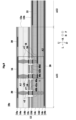
- FIG. 1 is an exploded perspective view of an antenna component 10.
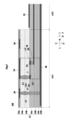
- FIG. FIG. 2 is a cross-sectional view of the antenna component 10 taken along line AA.
- FIG. 3 is a rear view of the antenna component 10 in use.
- FIG. 4 is a cross-sectional view of the antenna component 10a.
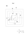
- FIG. 5 is a top view of the antenna component 10b.
- FIG. 6 is a cross-sectional view of the antenna component 10c.
- FIG. 7 is a cross-sectional view of the antenna component 10d.
- FIG. 8 is a cross-sectional view of the antenna component 10e.
- FIG. 9 is a cross-sectional view of the antenna component 10f.
- FIG. 10 is a cross-sectional view of the antenna component 10g.
- FIG. 11 is a top view of the antenna component 10h.
- Fig. 1 is an exploded perspective view of the antenna component 10.
- Fig. 2 is a cross-sectional view of the antenna component 10 taken along line A-A.
- Fig. 3 is a rear view of the antenna component 10 in use.
- the stacking direction of the main body 12 is parallel to the up-down axis.
- the up-down axis coincides with the Z axis.
- the upward direction is the positive direction of the Z axis.
- the downward direction is the negative direction of the Z axis.
- two sides of the main body 12 extend along the left-right axis.
- the remaining two sides of the main body 12 extend along the front-rear axis.
- the left-right axis is perpendicular to the up-down axis.
- the front-rear axis is perpendicular to the up-down axis and the left-right axis.
- the antenna component 10 is used, for example, in a wireless communication terminal such as a smartphone. As shown in FIG. 1, the antenna component 10 includes a main body 12, a first radiation conductor layer 16, a radiation member 17, a first ground conductor layer 28, a second ground conductor layer 30, a fourth ground conductor layer 31, a third ground conductor layer 32, a current path R, a plurality of interlayer connection conductors v2, and a plurality of interlayer connection conductors v5.
- the main body 12 has a plate shape. As shown in FIG. 1, the main body 12 has a rectangular shape when viewed from below.
- the main body 12 has a structure in which the first insulator layers 14a, 14b, the second insulator layers 14c to 14e, and the insulator layers 15a, 15b (multiple insulator layers) are stacked along the vertical axis (Z axis).
- the insulator layer 15a, the first insulator layers 14a, 14b, the second insulator layers 14c to 14e, and the insulator layer 15b are arranged in this order from top to bottom.
- the first insulator layers 14a, 14b have a rectangular shape when viewed from below.
- the second insulator layers 14c to 14e have a strip shape extending in the left-right direction when viewed from below.
- the first insulator layers 14a, 14b overlap the left ends of the second insulator layers 14c to 14e when viewed from below.
- the dielectric constant of the first insulator layers 14a, 14b is higher than that of the second insulator layers 14c to 14e.
- the first insulator layers 14a, 14b are, for example, a thermoplastic resin such as polyimide.
- the second insulator layers 14c to 14e are, for example, a thermoplastic resin such as a liquid crystal polymer.
- the first insulator layers 14a, 14b and the second insulator layers 14c to 14e are fused together with adjacent layers.
- the main body 12 is flexible.
- the insulator layers 15a, 15b will be described later.
- the first radiating conductor layer 16 and the radiating member 17 radiate and/or receive high-frequency signals.
- the first radiating conductor layer 16 is provided on the main body 12. In this embodiment, the first radiating conductor layer 16 is located on the upper main surface of the first insulator layer 14a. As shown in FIG. 1, the first radiating conductor layer 16 has a rectangular shape when viewed from below. As shown in FIG. 1, the first radiating conductor layer 16 has two sides extending along the front-to-back axis and two sides extending along the left-to-right axis when viewed from below. In the first radiating conductor layer 16, the left and right sides are longer than the front and rear sides.
- the radiating member 17 is provided on the main body 12.
- the radiating member 17 is located below the first radiating conductor layer 16 (on the negative side of the Z axis). More specifically, the radiating member 17 includes an interlayer connection conductor v21 and a second radiating conductor layer 18.
- the second radiating conductor layer 18 is provided on the main body 12.
- the second radiating conductor layer 18 is located on the lower main surface of the first insulating layer 14b.
- the second radiating conductor layer 18 is located below the first radiating conductor layer 16 (negative side of the Z axis).
- the second radiating conductor layer 18 has a rectangular shape when viewed downward.
- the second radiating conductor layer 18 has two sides extending along the front-rear axis and two sides extending along the left-right axis when viewed downward. In the second radiating conductor layer 18, the left and right sides are longer than the front and rear sides.
- the left side of the second radiating conductor layer 18 overlaps with the left side of the first radiating conductor layer 16.
- at least a portion of the second radiating conductor layer 18 overlaps with the first radiating conductor layer 16 when viewed downward (negative direction of the Z axis).
- the entire second radiating conductor layer 18 overlaps with the first radiating conductor layer 16 when viewed downward (negative direction of the Z axis).
- the area of the second radiating conductor layer 18 is smaller than the area of the first radiating conductor layer 16. Therefore, when viewed in the downward direction, the second radiating conductor layer 18 overlaps only the vicinity of the left edge of the first radiating conductor layer 16.
- the length of the second radiating conductor layer 18 in the front-to-rear direction is equal to the length of the first radiating conductor layer 16 in the front-to-rear direction.
- the second radiating conductor layer 18 when viewed from below, does not protrude from the first radiating conductor layer 16.
- the interlayer connection conductor v21 is provided in the main body 12.
- the interlayer connection conductor v21 penetrates the first insulator layers 14a, 14b (one or more of the multiple insulator layers) along the vertical axis (Z axis).
- the interlayer connection conductor v21 connects the first radiating conductor layer 16 and the second radiating conductor layer 18. Therefore, the upper end (the end on the positive side of the Z axis) of the interlayer connection conductor v21 is in contact with the first radiating conductor layer 16.
- the lower end (the end on the negative side of the Z axis) of the interlayer connection conductor v21 is in contact with the second radiating conductor layer 18.
- the radiating member 17 is connected to the first radiating conductor layer 16. However, the radiating member 17 is not connected to ground potential.
- the first ground conductor layer 28 is provided on the main body 12 as shown in FIG. 1. More specifically, the first ground conductor layer 28 is located below the first radiation conductor layer 16 (negative side of the Z axis). The first ground conductor layer 28 is located on the lower main surface of the second insulator layer 14e. As shown in FIG. 1, the first ground conductor layer 28 has a rectangular shape when viewed from below. The first ground conductor layer 28 covers almost the entire lower main surface of the second insulator layer 14e. As a result, the first ground conductor layer 28 overlaps with the first radiation conductor layer 16 when viewed from the downward direction (negative direction of the Z axis). The first ground conductor layer 28 is connected to a ground potential. As a result, the first radiation conductor layer 16, the radiating member 17, and the first ground conductor layer 28 form a patch antenna.
- the direction in which the electric field resonates in the first radiating conductor layer 16 is defined as the resonance direction.
- the resonance direction is the left-right direction.
- the direction perpendicular to the resonance direction when viewed downward (negative direction of the Z axis) is defined as the orthogonal direction.
- the orthogonal direction is the front-back direction.
- the length of the first radiating conductor layer 16 in the orthogonal direction is longer than the length of the first radiating conductor layer 16 in the resonance direction. Therefore, in the first radiating conductor layer 16, the left and right sides are longer than the front and rear sides.
- the length of the second radiating conductor layer 18 in the orthogonal direction is equal to the length of the first radiating conductor layer 16 in the orthogonal direction.
- the second ground conductor layer 30 is provided on the main body 12 as shown in FIG. 1. More specifically, the second ground conductor layer 30 is located on the upper main surface of the first insulator layer 14a. As a result, the second ground conductor layer 30 is located above the first ground conductor layer 28 (on the positive side of the Z axis).
- the second ground conductor layer 30 when viewed in the downward direction (negative direction of the Z axis), has a ring shape surrounding the first radiation conductor layer 16.
- the outer edge and inner edge of the second ground conductor layer 30 have a rectangular shape with two sides extending along the front-to-back axis and two sides extending along the left-to-right axis.
- the second ground conductor layer 30 does not overlap the first radiation conductor layer 16 when viewed in the downward direction (negative direction of the Z axis).
- the second ground conductor layer 30 is connected to the ground potential.
- the fourth ground conductor layer 31 is provided on the main body 12 as shown in FIG. 1. More specifically, the fourth ground conductor layer 31 is located on the lower main surface of the first insulator layer 14b. As a result, the fourth ground conductor layer 31 is located above the first ground conductor layer 28 (on the positive side of the Z axis).
- the fourth ground conductor layer 31 when viewed in the downward direction (negative direction of the Z axis), has a ring shape surrounding the first radiation conductor layer 16.
- the outer edge and inner edge of the fourth ground conductor layer 31 have a rectangular shape with two sides extending along the front-to-back axis and two sides extending along the left-to-right axis.
- the fourth ground conductor layer 31 does not overlap the first radiation conductor layer 16 when viewed in the downward direction.
- the fourth ground conductor layer 31 is connected to the ground potential.
- a high-frequency signal is transmitted through the current path R.
- the current path R is connected to the first radiation conductor layer 16.
- the current path R includes an interlayer connection conductor v1 and a signal conductor layer 20.
- the signal conductor layer 20 is provided on the main body 12. In this embodiment, the signal conductor layer 20 is located on the upper main surface of the second insulator layer 14d.
- the signal conductor layer 20 has a linear shape extending in the left-right direction. The left end of the signal conductor layer 20 overlaps with the first radiation conductor layer 16 when viewed in the downward direction.
- the interlayer connection conductor v1 is provided in the main body 12.
- the interlayer connection conductor v1 penetrates the first insulating layers 14a, 14b and the second insulating layer 14c along the up-down axis.
- the interlayer connection conductor v1 connects the first radiation conductor layer 16 and the signal conductor layer 20. Therefore, the upper end of the interlayer connection conductor v1 is in contact with the first radiation conductor layer 16.
- the position where the interlayer connection conductor v1 is in contact with the first radiation conductor layer 16 is the power supply point P.
- the lower end of the interlayer connection conductor v1 is in contact with the left end of the signal conductor layer 20.
- the third ground conductor layer 32 is provided on the main body 12 as shown in FIG. 1. More specifically, the third ground conductor layer 32 is located below the first radiation conductor layer 16 and above the signal conductor layer 20. The third ground conductor layer 32 is located on the upper main surface of the second insulator layer 14c. As shown in FIG. 1, the third ground conductor layer 32 has a rectangular shape when viewed downward. When viewed downward (negative direction of the Z axis), the third ground conductor layer 32 overlaps with the signal conductor layer 20. However, when viewed downward, the third ground conductor layer 32 does not overlap with the first radiation conductor layer 16. The third ground conductor layer 32 is connected to a ground potential. As a result, the signal conductor layer 20, the first ground conductor layer 28, and the third ground conductor layer 32 form a stripline structure.
- the insulator layer 15a covers the upper main surface of the first insulator layer 14a, the first radiation conductor layer 16, and the second ground conductor layer 30.
- the insulator layer 15b covers the lower main surface of the second insulator layer 14e and the first ground conductor layer 28.
- the insulator layers 15a and 15b are protective layers.
- the insulator layers 15a and 15b are solder resist.
- the material of the solder resist is, for example, epoxy resin or special acrylate.
- the lower end (end on the negative side of the Z axis) of the radiating member 17 is defined as the negative end t.
- the negative end t is the lower main surface of the second radiating conductor layer 18.
- the region that overlaps with the first radiating conductor layer 16 when viewed downward (negative direction of the Z axis) and is located above the negative end t (positive side of the Z axis) and below the first radiating conductor layer 16 (negative side of the Z axis) is defined as the first region A1.
- the region that overlaps with the first radiating conductor layer 16 when viewed downward (negative direction of the Z axis) and is located above the first ground conductor layer 28 (positive side of the Z axis) and below the negative end t (negative side of the Z axis) is defined as the second region A2.
- the first insulator layers 14a and 14b are located in the first region A1.
- the second insulator layers 14c to 14e are located in the second region A2.
- the composite dielectric constant of the first region A1 is higher than the composite dielectric constant of the second region A2.
- a method for calculating the complex dielectric constant will be described.
- An example will be given in which the first material to the nth material are present in the first region A1.
- n is a natural number.
- the dielectric constants of the first material to the nth material are ⁇ 1 to ⁇ n.
- the thicknesses of the first material to the nth material in the first region A1 on the vertical axis are d1 to dn.
- the complex dielectric constant ⁇ 0 is expressed by the following formula (1).
- ⁇ 0 (d1+d2+...+dn)/(d1/ ⁇ 1+d2/ ⁇ 2+...+dn/ ⁇ n)...(1)
- the multiple interlayer connection conductors v2 are provided on the main body 12.
- the multiple interlayer connection conductors v2 electrically connect the first ground conductor layer 28 and the second ground conductor layer 30. More specifically, the multiple interlayer connection conductors v2 penetrate the first insulator layers 14a, 14b and the second insulator layers 14c to 14e along the up-down axis. The upper ends of the multiple interlayer connection conductors v2 are in contact with the second ground conductor layer 30. The lower ends of the multiple interlayer connection conductors v2 are in contact with the first ground conductor layer 28.
- the multiple interlayer connection conductors v5 are provided on the main body 12.
- the multiple interlayer connection conductors v5 electrically connect the first ground conductor layer 28 and the second ground conductor layer 30. More specifically, the multiple interlayer connection conductors v5 penetrate the second insulator layers 14c to 14e along the up-down axis. The upper ends of the multiple interlayer connection conductors v5 are in contact with the second ground conductor layer 30. The lower ends of the multiple interlayer connection conductors v5 are in contact with the first ground conductor layer 28.
- the first radiation conductor layer 16, the radiation member 17, the signal conductor layer 20, the first ground conductor layer 28, the second ground conductor layer 30, the fourth ground conductor layer 31, and the third ground conductor layer 32 as described above are formed by patterning a metal foil attached to the upper or lower main surface of the first insulating layer 14a, 14b or the second insulating layer 14c to 14e.
- the metal foil is, for example, a copper foil.
- the interlayer connection conductors v1, v2, v5, and v21 are formed by filling a conductive paste into a through hole that penetrates the first insulating layer 14a, 14b or the second insulating layer 14c to 14e along the vertical axis, and solidifying the conductive paste by heating and pressurizing.
- the interlayer connection conductors v1, v2, v5, and v21 may be formed by plating the through hole.
- the antenna component 10 has a first section A11 and a second section A12.
- the first section A11 is a section that overlaps with the first insulator layers 14a, 14b when viewed from below.
- the second section A12 is a section that does not overlap with the first insulator layers 14a, 14b when viewed from below.
- the vertical thickness of the antenna component 10 in the second section A12 is smaller than the vertical thickness of the antenna component 10 in the first section A11. Therefore, the second section A12 is more easily deformed than the first section A11. Therefore, as shown in Fig. 3, the second section A12 is bent downward or upward.
- the radiating member 17 is connected to the first radiating conductor layer 16.
- the first radiating conductor layer 16 and the radiating member 17 form a patch antenna.
- the half wavelength of the high-frequency signal is equal to the sum of the left-right length of the first radiating conductor layer 16, the top-bottom length of the interlayer connection conductor v21, and the length from the interlayer connection conductor v21 to the right end of the second radiating conductor layer 18. Therefore, the left-right length of the first radiating conductor layer 16 may be short. This allows the antenna component 10 to be miniaturized when viewed in the downward direction.
- a large capacitance is likely to form between the radiating member 17 and the first ground conductor layer 28.
- the Q value of a resonant antenna such as a patch antenna becomes high. As a result, the antenna is likely to have a narrow bandwidth.
- the complex dielectric constant of the first region A1 is higher than the complex dielectric constant of the second region A2.
- the complex dielectric constant of the second region A2 is lower than the complex dielectric constant of the first region A1.
- the complex dielectric constant of the first region A1 is higher than the complex dielectric constant of the second region A2. This makes it easier for the wavelength shortening effect to occur in the first radiating conductor layer 16. As a result, the first radiating conductor layer 16 can be made smaller. Therefore, when viewed in the downward direction, the antenna component 10 can be made smaller.
- the area of the overlapping region in the second radiating conductor layer 18 that overlaps with the first radiating conductor layer 16 is greater than the area of the non-overlapping region in the second radiating conductor layer 18 that does not overlap with the first radiating conductor layer 16. This reduces the amount by which the second radiating conductor layer 18 protrudes from the first radiating conductor layer 16 when viewed in the downward direction. As a result, the antenna component 10 is made smaller when viewed in the downward direction.
- the resonance direction is the left-right direction. Therefore, current flows to the left or right.
- the length of the second radiating conductor layer 18 in the orthogonal direction is equal to the length of the first radiating conductor layer 16 in the orthogonal direction. This increases the length of the second radiating conductor layer 18 in the front-to-rear direction, thereby reducing the resistance of the second radiating conductor layer 18. As a result, the radiation efficiency of the antenna is improved.
- the resonance direction is the left-right direction. Therefore, current flows to the left or right.
- the length of the first radiating conductor layer 16 in the orthogonal direction is longer than the length of the first radiating conductor layer 16 in the resonance direction. Therefore, the length of the first radiating conductor layer 16 in the front-to-rear direction is longer, and the resistance of the first radiating conductor layer 16 is reduced. As a result, the radiation efficiency of the antenna is improved.
- the thickness of the antenna component 10 from top to bottom in the second section A12 is smaller than the thickness of the antenna component 10 from top to bottom in the first section A11. Therefore, the second section A12 is more easily deformed than the first section A11. Therefore, the second section A12 can be bent downward or upward.
- the second ground conductor layer 30 has a ring shape surrounding the first radiation conductor layer 16 when viewed from below. This makes it difficult for electromagnetic waves radiated by the first radiation conductor layer 16 to reach the components surrounding the antenna component 10. Also, it makes it difficult for electromagnetic waves radiated by the components surrounding the antenna component 10 to reach the first radiation conductor layer 16. Furthermore, the directivity of the antenna is improved.
- Fig. 4 is a cross-sectional view of the antenna component 10a.
- the antenna component 10a differs from the antenna component 10 in that the body 12 includes a first body portion 12a and a second body portion 12b. More specifically, the first body portion 12a includes first insulator layers 14a, 14b and insulator layers 15a, 15c. The insulator layer 15c covers the lower main surface of the first insulator layer 14b. The second body portion 12b includes second insulator layers 14c-14e and insulator layers 15b, 15d. The insulator layer 15d covers the upper main surface of the second insulator layer 14c.
- the antenna component 10a further includes mounting electrodes 40a-40d and solders 42a, 42b.
- the mounting electrodes 40a, 40c are located on the lower main surface of the first insulator layer 14b.
- the mounting electrode 40a is in contact with the lower end of the upper part of the interlayer connection conductor v2.
- the mounting electrode 40b is in contact with the upper end of the lower part of the interlayer connection conductor v2.
- the mounting electrodes 40b and 40d are located on the upper main surface of the second insulator layer 14c.
- the mounting electrode 40b is in contact with the lower end of the upper part of the interlayer connection conductor v1.
- the mounting electrode 40d is in contact with the upper end of the lower part of the interlayer connection conductor v1.
- Solder 42a is a conductive bonding material that connects mounting electrode 40a and mounting electrode 40b.
- Solder 42b is a conductive bonding material that connects mounting electrode 40c and mounting electrode 40d.
- the second region A2 contains the insulator layers 15c, 15d, air, and the second insulator layers 14c-14d. Therefore, the complex dielectric constant of the second region A2 is determined by the dielectric constant of the insulator layers 15c, 15d, the dielectric constant of the air, the dielectric constant of the second insulator layers 14c-14d, the volume of the insulator layers 15c, 15d, the volume of the air, and the volume of the second insulator layers 14c-14d.
- the rest of the structure of the antenna component 10a is the same as that of the antenna component 10, so a description will be omitted.
- the antenna component 10a can achieve the same effects as the antenna component 10.
- Fig. 5 is a top view of the antenna component 10b.
- the antenna component 10b differs from the antenna component 10 in that it further includes branch conductors 22a and 22b.
- the branch conductors 22a and 22b branch off from the current path R. More specifically, the branch conductor 22a branches off in the forward direction from the signal conductor layer 20.
- the branch conductor 22b branches off in the rear direction from the signal conductor layer 20. Therefore, the signal conductor layer 20 and the branch conductors 22a and 22b are included in one conductor layer.
- the branch conductors 22a and 22b are located on the lower main surface of the second insulator layer 14c. As a result, the branch conductors 22a and 22b are located in the second region A2.
- the branch conductors 22a and 22b overlap the first radiation conductor layer 16 when viewed in the downward direction (negative direction of the Z axis).
- the branch conductors 22a and 22b are located within a range of 1/2 or less of the wavelength of the high-frequency signal from the first radiation conductor layer 16.
- Such branch conductors 22a and 22b are open stubs. Therefore, the branch conductors 22a and 22b are not connected to any conductor layer other than the signal conductor layer 20.
- the rest of the structure of the antenna component 10b is the same as that of the antenna component 10, so a description thereof will be omitted.
- the antenna component 10b can achieve the same effects as the antenna component 10.
- branch conductors 22a and 22b branch off from the current path R.
- the branch conductors 22a and 22b play a role in matching the characteristic impedance of the first radiation conductor layer 16 with the characteristic impedance of the current path R.
- the reflection of high-frequency signals at the boundary between the first radiation conductor layer 16 and the current path R is suppressed, and the loss of high-frequency signals is reduced.
- the branch conductors 22a and 22b are not far away from the first radiating conductor layer 16 for the following reasons.
- reflection of the high-frequency signal occurs.
- the reflected high-frequency signal is reflected again at the branch conductors 22a and 22b.
- the reflected wave is radiated as an electromagnetic wave from the first radiating conductor layer 16. In this way, in the antenna component 10b, the reflected wave is used as an electromagnetic wave of the high-frequency signal.
- the branch conductors 22a, 22b are far away from the first radiation conductor layer 16, loss occurs in the reflected wave between the branch conductors 22a, 22b and the first radiation conductor layer 16. Therefore, it is preferable that the branch conductors 22a, 22b are not far away from the first radiation conductor layer 16.
- the branch conductors 22a, 22b are located within a range of 1/2 the wavelength of the high frequency signal from the first radiation conductor layer 16, so that the effect of the reflected wave due to impedance matching can be reduced, and loss can be reduced.
- Fig. 6 is a cross-sectional view of the antenna component 10c.
- Antenna component 10c differs from antenna component 10 in that it further includes a radiating member 117.
- the structure of radiating member 117 is symmetrical to radiating member 117 with respect to feeding point P, so a description thereof will be omitted.
- the rest of the structure of antenna component 10c is the same as that of antenna component 10, so a description thereof will be omitted.
- Antenna component 10c can achieve the same effects as antenna component 10.
- the antenna component 10c further includes a radiating member 117.
- the first radiating conductor layer 16 and the radiating members 17, 117 form a patch antenna.
- the half wavelength of the high-frequency signal is equal to the sum of the left-right length of the first radiating conductor layer 16, the top-bottom length of the interlayer connection conductor v21, the length from the interlayer connection conductor v21 to the right end of the second radiating conductor layer 18, the top-bottom length of the interlayer connection conductor v121, and the length from the interlayer connection conductor v121 to the left end of the second radiating conductor layer 118.
- the symmetry of the radiation characteristics of the antenna component 10c is improved.
- Fig. 7 is a cross-sectional view of the antenna component 10d.
- Antenna component 10d differs from antenna component 10 in that the second radiation conductor layer 18 is located on the lower main surface of the second insulator layer 14c.
- the rest of the structure of antenna component 10d is the same as that of antenna component 10, so a description thereof will be omitted.
- Antenna component 10d can achieve the same effects as antenna component 10.
- Fig. 8 is a cross-sectional view of the antenna component 10e.
- the antenna component 10e differs from the antenna component 10d in that the body 12 includes a first body portion 12a and a second body portion 12b.
- the second radiation conductor layer 18 is provided on the second body portion 12b.
- the rest of the structure of the antenna component 10e is the same as that of the antenna component 10d, so a description thereof will be omitted.
- the antenna component 10e can achieve the same effects as the antenna component 10d.
- Fig. 9 is a cross-sectional view of the antenna component 10f.
- the antenna component 10f is such that the upper end of the interlayer connection conductor v1 is not in contact with the first radiation conductor layer 16.
- the antenna component 10f further includes a power supply conductor layer 34.
- the power supply conductor layer 34 is located on the lower main surface of the first insulator layer 14b.
- the power supply conductor layer 34 also overlaps with the first radiation conductor layer 16 when viewed from below. This forms a capacitance between the first radiation conductor layer 16 and the power supply conductor layer 34.
- the upper end of the interlayer connection conductor v1 is in contact with the power supply conductor layer 34.
- the antenna component 10f described above high-frequency signals are transmitted between the power supply conductor layer 34 and the first radiation conductor layer 16 via capacitance between the first radiation conductor layer 16 and the power supply conductor layer 34.
- the rest of the structure of the antenna component 10f is the same as that of the antenna component 10, so a description thereof will be omitted.
- the antenna component 10f can achieve the same effects as the antenna component 10.
- Fig. 10 is a cross-sectional view of the antenna component 10g.
- the antenna component 10g differs from the antenna component 10 in that it further comprises an interlayer connection conductor v25.
- the interlayer connection conductor v25 connects the first radiation conductor layer 16 and the first ground conductor layer 28.
- the first radiation conductor layer 16, the radiating member 17, the first ground conductor layer 28, and the interlayer connection conductor v25 form an inverted F-shaped antenna. This allows the antenna length to be 1/4 wavelength, making the antenna component 10g smaller.
- the rest of the structure of the antenna component 10g is the same as that of the antenna component 10, so a description will be omitted.
- the antenna component 10g can achieve the same effects as the antenna component 10.
- Fig. 11 is a top view of the antenna component 10h.
- the antenna component 10h differs from the antenna component 10 in that the first radiation conductor layer 16 is connected to the second ground conductor layer 30.
- the first radiation conductor layer 16, the radiating member 17, the first ground conductor layer 28, and the second ground conductor layer 30 form an inverted F-shaped antenna.
- the rest of the structure of the antenna component 10h is the same as that of the antenna component 10, so a description thereof will be omitted.
- the antenna component 10h can achieve the same effects as the antenna component 10.
- antenna components according to the present invention are not limited to the antenna components 10, 10a to 10h, and may be modified within the scope of the present invention.
- the structures of the antenna components 10, 10a to 10h may be combined in any manner.
- the radiating member 17 may have a structure other than that shown in the figure.
- the radiating member 17 may further include an interlayer connection conductor and a second radiating conductor layer.
- the second radiating conductor layer is connected to the second radiating conductor layer 18 via the interlayer connection conductor.
- the second radiating conductor layer may be located below the second radiating conductor layer 18 or may be located above the second radiating conductor layer 18.
- the radiating member 17 may include only the interlayer connecting conductor v21.
- the second ground conductor layer 30 is not a required component.
- the second radiating conductor layer 18 may protrude from the first radiating conductor layer 16.
- the area of the overlapping region of the second radiating conductor layer 18 that overlaps with the first radiating conductor layer 16 may be larger than the area of the non-overlapping region of the second radiating conductor layer 18 that does not overlap with the first radiating conductor layer 16, or it may not be larger than the area of the non-overlapping region of the second radiating conductor layer 18 that does not overlap with the first radiating conductor layer 16.
- the length of the second radiating conductor layer 18 in the orthogonal direction does not have to be equal to the length of the first radiating conductor layer 16 in the orthogonal direction.
- the length of the first radiating conductor layer 16 in the orthogonal direction may be less than or equal to the length of the first radiating conductor layer 16 in the resonance direction.
- branch conductors 22a and 22b do not have to overlap with the first radiation conductor layer 16 when viewed from below.
- branch conductors 22a and 22b may be short stubs.
- the branch conductors 22a and 22b may be located in the first region A1.
- the material of the first insulating layers 14a and 14b may be ceramic, and the material of the second insulating layers 14c to 14e may be liquid crystal polymer or polyimide.
- the material of the first insulating layers 14a and 14b may be liquid crystal polymer containing a filler, and the material of the second insulating layers 14c to 14e may be liquid crystal polymer. In this case, the dielectric constant of the filler is lower than the dielectric constant of the liquid crystal polymer.
- the material of the first insulating layers 14a and 14b may be polyimide containing a filler, and the material of the second insulating layers 14c to 14e may be polyimide. In this case, the dielectric constant of the filler is lower than the dielectric constant of polyimide.
- the first body portion 12a is an electronic component that does not have flexibility.
- the second body portion 12b is a flexible circuit board. In this case, the first section A11 cannot bend, but the second section A12 can bend.
- the antenna components 10, 10a to 10h may not have the second section A12.
- an external electrode is provided on the lower main surface of the second insulator layer 14e.
- the lower end of the interlayer connection conductor v1 contacts the external electrode.
- the power supply conductor layer 34 may be located above the second insulator layers 14c to 14e. This reduces the number of interlayer connection conductors in the antenna component 10f.
- the second radiating conductor layer 18 may protrude from the first radiating conductor layer 16.
- the area of the overlapping region in the second radiating conductor layer 18 that overlaps with the first radiating conductor layer 16 is greater than the area of the non-overlapping region in the second radiating conductor layer 18 that does not overlap with the first radiating conductor layer 16.
- the present invention has the following structure:
- the antenna component includes a body, a first radiation conductor layer, a radiation member, and a first ground conductor layer;
- the main body has a structure in which a plurality of insulating layers are arranged along the Z axis, the first radiating conductor layer is provided on the body, the radiating member is provided on the main body, is located on the negative side of the Z-axis from the first radiating conductor layer, is connected to the first radiating conductor layer, and is not connected to a ground potential;
- the first ground conductor layer is provided on the main body, overlaps the first radiation conductor layer and the radiating member when viewed in the negative direction of the Z axis, and is located on the negative side of the Z axis with respect to the first radiation conductor layer;
- the end of the radiating member on the negative side of the Z axis is defined as a negative end, a region overlapping with the first radiating conductor layer when viewed in the negative direction of the Z axis, the region being located on the positive side of
- the radiating member includes an interlayer connection conductor and a second radiating conductor layer, the second radiating conductor layer is provided on the main body and is located on the negative side of the Z axis relative to the first radiating conductor layer; the interlayer connection conductor is provided in the body, and penetrates one or more of the plurality of insulator layers along the Z-axis, and connects the first radiation conductor layer and the second radiation conductor layer; When viewed in the negative direction of the Z axis, the area of the second radiating conductor layer is smaller than the area of the first radiating conductor layer.
- An antenna component as described in (1).
- an area of an overlapping region in the second radiating conductor layer that overlaps with the first radiating conductor layer is larger than an area of a non-overlapping region in the second radiating conductor layer that does not overlap with the first radiating conductor layer.
- a direction in which an electric field resonates in the first radiation conductor layer is defined as a resonance direction;
- a direction perpendicular to the resonance direction is defined as an orthogonal direction,
- the length of the second radiating conductor layer in the orthogonal direction is equal to the length of the first radiating conductor layer in the orthogonal direction.
- a direction in which an electric field resonates in the first radiation conductor layer is defined as a resonance direction;
- a direction perpendicular to the resonance direction is defined as an orthogonal direction, a length of the first radiating conductor layer in the orthogonal direction is longer than a length of the first radiating conductor layer in the resonance direction;
- the antenna component further includes a second ground conductor layer, the second ground conductor layer is provided on the main body and has a ring shape surrounding the first radiation conductor layer when viewed in the negative direction of the Z axis.
- An antenna component according to any one of (1) to (6).
- the antenna component further comprises a current path, the current path is connected to the first radiation conductor layer; A high-frequency signal is transmitted through the current path.
- An antenna component according to any one of (1) to (7).
- the antenna component further comprises a branch conductor, The branch conductor branches off from the current path.
- the branch conductor is located within a range of 1 ⁇ 2 or less of the wavelength of the high frequency signal from the first radiation conductor layer.
- the branch conductor is located in the second region.
- the plurality of insulator layers include a first insulator layer and a second insulator layer; the first insulating layer is located in the first region; the second insulating layer is located in the second region; The dielectric constant of the first insulating layer is higher than the dielectric constant of the second insulating layer.
Landscapes
- Engineering & Computer Science (AREA)
- Microelectronics & Electronic Packaging (AREA)
- Details Of Aerials (AREA)
Priority Applications (2)
| Application Number | Priority Date | Filing Date | Title |
|---|---|---|---|
| JP2025500734A JP7810309B2 (ja) | 2023-02-16 | 2024-01-18 | アンテナ部品 |
| US19/294,733 US20250364722A1 (en) | 2023-02-16 | 2025-08-08 | Antenna component |
Applications Claiming Priority (2)
| Application Number | Priority Date | Filing Date | Title |
|---|---|---|---|
| JP2023022151 | 2023-02-16 | ||
| JP2023-022151 | 2023-02-16 |
Related Child Applications (1)
| Application Number | Title | Priority Date | Filing Date |
|---|---|---|---|
| US19/294,733 Continuation US20250364722A1 (en) | 2023-02-16 | 2025-08-08 | Antenna component |
Publications (1)
| Publication Number | Publication Date |
|---|---|
| WO2024171710A1 true WO2024171710A1 (ja) | 2024-08-22 |
Family
ID=92421407
Family Applications (1)
| Application Number | Title | Priority Date | Filing Date |
|---|---|---|---|
| PCT/JP2024/001284 Ceased WO2024171710A1 (ja) | 2023-02-16 | 2024-01-18 | アンテナ部品 |
Country Status (3)
| Country | Link |
|---|---|
| US (1) | US20250364722A1 (https=) |
| JP (1) | JP7810309B2 (https=) |
| WO (1) | WO2024171710A1 (https=) |
Citations (4)
| Publication number | Priority date | Publication date | Assignee | Title |
|---|---|---|---|---|
| WO2015083457A1 (ja) * | 2013-12-03 | 2015-06-11 | 株式会社村田製作所 | パッチアンテナ |
| JP2020088493A (ja) * | 2018-11-20 | 2020-06-04 | Tdk株式会社 | アンテナモジュール |
| WO2021182037A1 (ja) * | 2020-03-09 | 2021-09-16 | 株式会社村田製作所 | アンテナモジュールおよびそれを搭載する通信装置 |
| WO2021210297A1 (ja) * | 2020-04-14 | 2021-10-21 | 株式会社村田製作所 | 多層基板 |
-
2024
- 2024-01-18 WO PCT/JP2024/001284 patent/WO2024171710A1/ja not_active Ceased
- 2024-01-18 JP JP2025500734A patent/JP7810309B2/ja active Active
-
2025
- 2025-08-08 US US19/294,733 patent/US20250364722A1/en active Pending
Patent Citations (4)
| Publication number | Priority date | Publication date | Assignee | Title |
|---|---|---|---|---|
| WO2015083457A1 (ja) * | 2013-12-03 | 2015-06-11 | 株式会社村田製作所 | パッチアンテナ |
| JP2020088493A (ja) * | 2018-11-20 | 2020-06-04 | Tdk株式会社 | アンテナモジュール |
| WO2021182037A1 (ja) * | 2020-03-09 | 2021-09-16 | 株式会社村田製作所 | アンテナモジュールおよびそれを搭載する通信装置 |
| WO2021210297A1 (ja) * | 2020-04-14 | 2021-10-21 | 株式会社村田製作所 | 多層基板 |
Also Published As
| Publication number | Publication date |
|---|---|
| JP7810309B2 (ja) | 2026-02-03 |
| JPWO2024171710A1 (https=) | 2024-08-22 |
| US20250364722A1 (en) | 2025-11-27 |
Similar Documents
| Publication | Publication Date | Title |
|---|---|---|
| US9837697B2 (en) | Radio frequency connection arrangement | |
| US9882256B2 (en) | High-frequency signal transmission line and electronic apparatus | |
| US9401534B2 (en) | High-frequency signal line and electronic device | |
| US9705194B2 (en) | Antenna module | |
| JP2013197787A (ja) | アンテナ装置及び電子装置 | |
| WO2012070213A1 (ja) | アンテナ装置 | |
| US11018434B2 (en) | Antenna apparatus, and manufacturing method | |
| JP2005312062A (ja) | 小型アンテナ | |
| US12046838B2 (en) | Multilayer board | |
| GB2382231A (en) | Isolator device for RF radiators | |
| WO2024069858A1 (ja) | 伝送装置及びアンテナ | |
| WO2019216188A1 (ja) | 伝送線路及びその実装構造 | |
| JP7810309B2 (ja) | アンテナ部品 | |
| CN223156273U (zh) | 多层基板 | |
| CN102918710B (zh) | 天线辐射单元、馈电方法及天线系统 | |
| JP7425554B2 (ja) | アンテナ装置 | |
| JP7803439B2 (ja) | 多層基板 | |
| WO2016128766A2 (en) | RADIO FREQUENCY CONNECTION ARRANGEMENt | |
| US20250239772A1 (en) | Multilayer substrate | |
| US20250226582A1 (en) | Antenna module | |
| JP2026005758A (ja) | アンテナ装置 | |
| JP2006157812A (ja) | アンテナ装置 |
Legal Events
| Date | Code | Title | Description |
|---|---|---|---|
| 121 | Ep: the epo has been informed by wipo that ep was designated in this application |
Ref document number: 24756561 Country of ref document: EP Kind code of ref document: A1 |
|
| WWE | Wipo information: entry into national phase |
Ref document number: 2025500734 Country of ref document: JP |
|
| NENP | Non-entry into the national phase |
Ref country code: DE |
|
| 122 | Ep: pct application non-entry in european phase |
Ref document number: 24756561 Country of ref document: EP Kind code of ref document: A1 |